WO2017013938A1 - Module haute fréquence - Google Patents
Module haute fréquence Download PDFInfo
- Publication number
- WO2017013938A1 WO2017013938A1 PCT/JP2016/065166 JP2016065166W WO2017013938A1 WO 2017013938 A1 WO2017013938 A1 WO 2017013938A1 JP 2016065166 W JP2016065166 W JP 2016065166W WO 2017013938 A1 WO2017013938 A1 WO 2017013938A1
- Authority
- WO
- WIPO (PCT)
- Prior art keywords
- antenna
- sealing resin
- post
- frequency module
- groove
- Prior art date
- Legal status (The legal status is an assumption and is not a legal conclusion. Google has not performed a legal analysis and makes no representation as to the accuracy of the status listed.)
- Ceased
Links
Images



Classifications
-
- H—ELECTRICITY
- H01—ELECTRIC ELEMENTS
- H01Q—ANTENNAS, i.e. RADIO AERIALS
- H01Q1/00—Details of, or arrangements associated with, antennas
- H01Q1/12—Supports; Mounting means
- H01Q1/22—Supports; Mounting means by structural association with other equipment or articles
- H01Q1/2283—Supports; Mounting means by structural association with other equipment or articles mounted in or on the surface of a semiconductor substrate as a chip-type antenna or integrated with other components into an IC package
-
- H—ELECTRICITY
- H01—ELECTRIC ELEMENTS
- H01Q—ANTENNAS, i.e. RADIO AERIALS
- H01Q1/00—Details of, or arrangements associated with, antennas
- H01Q1/36—Structural form of radiating elements, e.g. cone, spiral, umbrella; Particular materials used therewith
- H01Q1/38—Structural form of radiating elements, e.g. cone, spiral, umbrella; Particular materials used therewith formed by a conductive layer on an insulating support
-
- H—ELECTRICITY
- H01—ELECTRIC ELEMENTS
- H01Q—ANTENNAS, i.e. RADIO AERIALS
- H01Q23/00—Antennas with active circuits or circuit elements integrated within them or attached to them
-
- H—ELECTRICITY
- H01—ELECTRIC ELEMENTS
- H01Q—ANTENNAS, i.e. RADIO AERIALS
- H01Q9/00—Electrically-short antennas having dimensions not more than twice the operating wavelength and consisting of conductive active radiating elements
- H01Q9/04—Resonant antennas
- H01Q9/30—Resonant antennas with feed to end of elongated active element, e.g. unipole
- H01Q9/42—Resonant antennas with feed to end of elongated active element, e.g. unipole with folded element, the folded parts being spaced apart a small fraction of the operating wavelength
-
- H—ELECTRICITY
- H05—ELECTRIC TECHNIQUES NOT OTHERWISE PROVIDED FOR
- H05K—PRINTED CIRCUITS; CASINGS OR CONSTRUCTIONAL DETAILS OF ELECTRIC APPARATUS; MANUFACTURE OF ASSEMBLAGES OF ELECTRICAL COMPONENTS
- H05K1/00—Printed circuits
- H05K1/02—Details
- H05K1/14—Structural association of two or more printed circuits
-
- H—ELECTRICITY
- H10—SEMICONDUCTOR DEVICES; ELECTRIC SOLID-STATE DEVICES NOT OTHERWISE PROVIDED FOR
- H10W—GENERIC PACKAGES, INTERCONNECTIONS, CONNECTORS OR OTHER CONSTRUCTIONAL DETAILS OF DEVICES COVERED BY CLASS H10
- H10W44/00—Electrical arrangements for controlling or matching impedance
- H10W44/20—Electrical arrangements for controlling or matching impedance at high-frequency [HF] or radio frequency [RF]
-
- H—ELECTRICITY
- H10—SEMICONDUCTOR DEVICES; ELECTRIC SOLID-STATE DEVICES NOT OTHERWISE PROVIDED FOR
- H10W—GENERIC PACKAGES, INTERCONNECTIONS, CONNECTORS OR OTHER CONSTRUCTIONAL DETAILS OF DEVICES COVERED BY CLASS H10
- H10W72/00—Interconnections or connectors in packages
-
- H—ELECTRICITY
- H10—SEMICONDUCTOR DEVICES; ELECTRIC SOLID-STATE DEVICES NOT OTHERWISE PROVIDED FOR
- H10W—GENERIC PACKAGES, INTERCONNECTIONS, CONNECTORS OR OTHER CONSTRUCTIONAL DETAILS OF DEVICES COVERED BY CLASS H10
- H10W72/00—Interconnections or connectors in packages
- H10W72/30—Die-attach connectors
-
- H—ELECTRICITY
- H10—SEMICONDUCTOR DEVICES; ELECTRIC SOLID-STATE DEVICES NOT OTHERWISE PROVIDED FOR
- H10W—GENERIC PACKAGES, INTERCONNECTIONS, CONNECTORS OR OTHER CONSTRUCTIONAL DETAILS OF DEVICES COVERED BY CLASS H10
- H10W76/00—Containers; Fillings or auxiliary members therefor; Seals
- H10W76/10—Containers or parts thereof
- H10W76/12—Containers or parts thereof characterised by their shape
-
- H—ELECTRICITY
- H10—SEMICONDUCTOR DEVICES; ELECTRIC SOLID-STATE DEVICES NOT OTHERWISE PROVIDED FOR
- H10W—GENERIC PACKAGES, INTERCONNECTIONS, CONNECTORS OR OTHER CONSTRUCTIONAL DETAILS OF DEVICES COVERED BY CLASS H10
- H10W90/00—Package configurations
-
- H—ELECTRICITY
- H10—SEMICONDUCTOR DEVICES; ELECTRIC SOLID-STATE DEVICES NOT OTHERWISE PROVIDED FOR
- H10W—GENERIC PACKAGES, INTERCONNECTIONS, CONNECTORS OR OTHER CONSTRUCTIONAL DETAILS OF DEVICES COVERED BY CLASS H10
- H10W44/00—Electrical arrangements for controlling or matching impedance
- H10W44/20—Electrical arrangements for controlling or matching impedance at high-frequency [HF] or radio frequency [RF]
- H10W44/241—Electrical arrangements for controlling or matching impedance at high-frequency [HF] or radio frequency [RF] for passive devices or passive elements
- H10W44/248—Electrical arrangements for controlling or matching impedance at high-frequency [HF] or radio frequency [RF] for passive devices or passive elements for antennas
-
- H—ELECTRICITY
- H10—SEMICONDUCTOR DEVICES; ELECTRIC SOLID-STATE DEVICES NOT OTHERWISE PROVIDED FOR
- H10W—GENERIC PACKAGES, INTERCONNECTIONS, CONNECTORS OR OTHER CONSTRUCTIONAL DETAILS OF DEVICES COVERED BY CLASS H10
- H10W90/00—Package configurations
- H10W90/701—Package configurations characterised by the relative positions of pads or connectors relative to package parts
- H10W90/751—Package configurations characterised by the relative positions of pads or connectors relative to package parts of bond wires
- H10W90/754—Package configurations characterised by the relative positions of pads or connectors relative to package parts of bond wires between a chip and a stacked insulating package substrate, interposer or RDL
Definitions
- the present invention relates to a high frequency module, and more particularly to a high frequency module provided with an antenna.
- Patent Document 1 discloses a high-frequency module having a structure in which an antenna is formed on a sealing resin on a wiring board and the wiring board and the antenna are electrically connected.
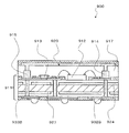
- a semiconductor device 900 which is such a high-frequency module will be described with reference to FIG.
- the semiconductor device 900 includes a wiring substrate 911 having a power feeding layer 924 and a ground conductive layer 927, and an inverted F antenna on a sealing resin 917 covering the semiconductor chip 912 and the chip component 913 connected on the wiring substrate 911. 920 is provided, and the inverted F-type antenna 920 is electrically connected to the feeding layer 924 and the ground conductive layer 927.
- the inverted F-type antenna 920 and the power feeding layer 924 are connected by solder via a terminal 914 disposed on the connection portion 932B connected to the power feeding layer 924.
- the inverted F-type antenna 920 and the ground conductive layer 927 are connected by solder via a terminal 915 provided on the connection portion 933B connected to the ground conductive layer 927.
- the terminals 914 and 915 have a block shape, and a conductive material such as copper is used as the material thereof.
- the connecting portion between the inverted F-type antenna 920 and the terminal 914 and the connecting portion between the inverted F-type antenna 920 and the terminal 915 are surrounded by the sealing resin 917.
- Such a configuration has the effect of providing a semiconductor device that can be reduced in size and reduced in cost.
- the terminal 914 and the terminal 915 are made of a conductive material, that is, a metal.
- a material of the sealing resin 917 for example, a mold resin is used.
- the metal and resin have different thermal expansion coefficients, and the thermal expansion coefficient of the resin is higher than the thermal expansion coefficient of the metal. For this reason, there is a possibility that the connection portion between the inverted F-type antenna 920 and the terminal 914 and the connection portion between the inverted F-type antenna 920 and the terminal 915 are peeled off due to a high ambient temperature and disconnected. For this reason, the reliability of the semiconductor device 900 is reduced.
- the present invention has been made in view of the actual situation of the prior art, and an object thereof is to provide a high-reliability high-frequency module.
- a high-frequency module includes a wiring board, a high-frequency circuit composed of circuit components disposed on the upper surface of the wiring board, and a metal post disposed on the upper surface of the wiring board. And a sealing resin that covers the circuit component, and an antenna substrate that is provided on the upper surface of the sealing resin and has an antenna formed by a metal pattern, and the groove is provided in the sealing resin And at least a part of the post is exposed from the groove, and on the upper side of the post, a central surface and two opposing side wall surfaces positioned higher than the central surface are formed.
- the conductive adhesive is adhered to the central surface of the post, the two side wall surfaces, and the antenna.
- the conductive adhesive is bonded on the three surfaces of the center surface of the metal post and the two side wall surfaces, the conductive adhesive may be peeled off. It is low and the possibility that the connection between the antenna and the high-frequency circuit on the wiring board is broken is also reduced. As a result, a highly reliable high frequency module can be provided.
- the sealing resin is provided in a rectangular shape, and the groove provided in the sealing resin is configured such that one side of the sealing resin provided in the rectangular shape is opposed to the one side.
- the circuit component is composed of a first circuit component and a second circuit component shorter than the first circuit component, and the second circuit component is formed in the groove. It has the feature of being arranged on the lower side.
- the high-frequency module configured in this manner has the second short circuit component disposed below the groove, a plurality of circuit components can be efficiently disposed on the wiring board. As a result, it is possible to contribute to miniaturization of the high frequency module.
- a side through hole is provided on a side surface of the antenna substrate, and an electrode part is formed in the side through hole, and the electrode part is formed of the conductive adhesive. Is connected to the post.
- the high-frequency module configured in this way has the electrode part formed in the side through hole, the electrode part and the post can be easily connected.
- the conductive adhesive is bonded on the three surfaces of the center surface of the metal post and the two side wall surfaces, the possibility that the conductive adhesive is peeled off is low. There is also a low possibility that the connection with the high-frequency circuit on the wiring board is broken. As a result, a highly reliable high frequency module can be provided.
- the high-frequency module 100 of the present invention is a small high-frequency module having an antenna, which is used in, for example, a wireless LAN (Local Area Network).
- the use of the high-frequency module 100 of the present invention is not limited to the embodiments described below, and can be changed as appropriate.
- FIG. 1 is a perspective view showing an appearance of the high-frequency module 100
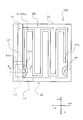
- FIG. 2 is a plan view of the high-frequency module 100 as viewed from above.
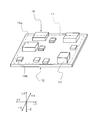
- 3 is a perspective view of the wiring board 10 on which the circuit components 15 are arranged
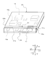
- FIG. 4 is a perspective view showing the sealing resin 30 and the wiring board 10 in which the grooves 31 are formed.
- FIG. 5 the two-dot chain line indicates that the conductive adhesive 13 is transparent.
- the high-frequency module 100 is arranged on a rectangular wiring board 10, a sealing resin 30 covering the wiring board 10, and an upper surface of the sealing resin 30, and has an area larger than that of the wiring board 10.
- An antenna substrate 20 having a small rectangular shape.
- an antenna 21 formed by a conductive metal pattern 21a is formed on the antenna substrate 20, and an antenna 21 and the high frequency circuit 11 are connected to each other.
- the high-frequency module 100 is manufactured by cutting a collective substrate (not shown) composed of a plurality of wiring substrates 10, a plurality of antenna substrates 20, and a plurality of sealing resins 30.
- the antenna 21 employs a monopole antenna having a meander shape and an open end 21 b in this embodiment.
- other antennas such as an inverted F antenna are used. It may be.
- a side through hole 29 is provided on the side surface of the antenna substrate 20, and an electrode portion 27 is formed in the side through hole 29.
- the electrode portion 27 is formed by cutting the side through hole 29 in the collective substrate state in the Z direction.
- the electrode part 27 is connected to the feeding end 21 c of the antenna 21.
- the electrode portion 27 is provided at the end portion on the ⁇ Y side of one side on the ⁇ X side of the antenna substrate 20 shown in FIG. 1, and the side electrode portion 27 a formed in the side through hole 29 and the side through portion.
- the lower electrode portion 27 b formed on the lower surface of the hole 29 is configured.
- the electrode part 27 composed of the side electrode part 27 a and the lower electrode part 27 b is connected to the high frequency circuit 11 by the conductive adhesive 13.
- an electrode portion 28 is provided on the other side of the + X side opposite to one side on the ⁇ X side of the antenna substrate 20 on which the electrode portion 27 is provided. Neither the high-frequency circuit 11 of the substrate 10 nor the antenna 21 on the antenna substrate 20 is connected. This electrode portion 28 is a part of the electrode portion of another antenna substrate on the collective substrate formed when the antenna substrate 20 formed by cutting the collective substrate is manufactured. It is not used and does not affect the high frequency module 100.
- a plurality of circuit components 15 such as integrated circuits are disposed on the wiring board 10 before the sealing resin 30 is formed, and are attached to the wiring board 10 by soldering.
- the circuit component 15 includes a first circuit component 15a and a second circuit component 15b that is shorter than the first circuit component 15a.
- Each of the plurality of circuit components 15 is connected by a wiring pattern (not shown) to form the high frequency circuit 11.
- the antenna 21 is connected to the high-frequency circuit 11, and a high-frequency signal transmitted or received by the antenna 21 is subjected to signal processing.
- the circuit component 15 is disposed on the wiring substrate 10 and at the same time, a metal post 17 is disposed and attached to the wiring substrate 10 by soldering.
- the post 17 is connected to the high-frequency circuit 11 by a wiring pattern (not shown).
- a sealing resin 30 is formed on the wiring substrate 10 to which the plurality of circuit components 15 and the posts 17 are attached. As shown in FIG. 4, the sealing resin 30 is formed in a rectangular shape so as to cover the circuit component 15 and the post 17 over almost the entire area of the wiring substrate 10.
- a groove 31 is provided in the sealing resin 30. As shown in FIG. 4, the groove 31 extends along the ⁇ X side side of the sealing resin 30 provided in a rectangular shape and from the ⁇ Y side one side 30a to the other side of the + Y side facing the one side 30a. It is provided with the same width up to 30b.
- the high-frequency module 100 is manufactured by cutting the aggregate substrate.
- the groove 31 is provided in the sealing resin 30, after forming the sealing resin 30 in the state of the collective substrate, the groove 31 is formed in the state of the collective substrate.
- a dicing apparatus is used to form the groove 31.
- the dicing apparatus a dicing apparatus used when cutting an aggregate substrate completed as a plurality of high-frequency modules into individual high-frequency modules 100 is used. Therefore, a new device for forming the groove 31 is not required.
- the groove 31 is formed on the side opposite to the side where the open end 21b of the antenna 21 is located, that is, the side where the feeding end 21c is located.
- the groove 31 is formed so as to cross the central portion in the X direction of the post 17 attached on the wiring board 10.
- the groove 31 is constituted by a bottom 31a and two opposing side walls 31b.
- the position of the bottom 31 a of the groove 31 from the upper surface of the wiring substrate 10 is set lower than the position of the upper surface of the post 17. Therefore, after the groove 31 is formed, the central portion of the post 17 made of metal is cut out with the same width as the width of the groove 31 in the Y direction.
- the post 17 is formed in a U shape in a sectional view as shown in FIG.
- the circuit component 15 is composed of the first circuit component 15a which is tall and the second circuit component 15b which is shorter than the first circuit component 15a.
- the tall first circuit component 15a is not arranged, and the short second circuit component 15b is arranged.
- the height of the second circuit component 15 b from the upper surface of the wiring board 10 is set lower than the position of the bottom 31 a of the groove 31 from the upper surface of the wiring board 10. For this reason, even if the second circuit component 15 b is disposed below the groove 31, the upper part of the second circuit component 15 b does not protrude upward from the bottom 31 a of the groove 31.
- the antenna substrate 20 is disposed on the upper surface of the sealing resin 30 as shown in FIG.
- FIG. 6 is an enlarged cross-sectional view showing a connection portion between the electrode portion 27 and the post 17 when viewed from the line AA shown in FIG.
- the post 17 disposed on the wiring board 10 is formed in a U shape in a sectional view.
- the post 17 is formed in a U-shape in cross section, as shown in FIGS. 5 and 6, on the upper side of the post 17, there are a central surface 17 a and two opposing sides that are higher than the central surface 17 a.
- a wall surface 17b is formed. Accordingly, at least a part of the post 17, that is, the central surface 17 a and the side wall surface 17 b are exposed from the groove 31.
- the central surface 17a and the side wall surface 17b of the post 17 constitute a part of the bottom portion 31a and the side wall portion 31b of the groove 31, respectively.
- the post 17 is already connected to the high-frequency circuit 11 formed on the wiring board 10 by a wiring pattern (not shown).
- a non-conductive adhesive (not shown) is applied to substantially the center of the upper surface of the sealing resin 30, and A conductive adhesive 13 such as silver paste is applied to a part of the upper surface.
- the conductive adhesive 13 is applied to the upper surface of the sealing resin 30 around the place where the electrode portion 27 of the antenna substrate 20 is disposed, and as shown in FIGS. 5 and 6.
- the post 17 is applied so as to fill a portion surrounded by the bottom portion 31a and the two side wall portions 31b of the groove 31 including a portion surrounded by the center surface 17a and the two side wall surfaces 17b.
- the substantially central portion of the antenna substrate 20 is bonded to the upper surface of the sealing resin 30 with a non-conductive adhesive and the antenna substrate 20.
- the lower electrode portion 27 b of the electrode portion 27 is bonded to the upper surface of the sealing resin 30 by the conductive adhesive 13.
- the conductive adhesive 13 adheres to the side electrode part 27 a of the electrode part 27.
- the conductive adhesive 13 is adhered to the central surface 17 a of the post 17 and the two side wall surfaces 17 b of the post 17.
- the electrode portion 27 of the antenna substrate 20 is reliably connected to the post 17 on the wiring substrate 10. That is, the antenna 21 and the high frequency circuit 11 are securely connected.
- connection part between the electrode part 27 made of metal and the metal post 17 is not surrounded by the sealing resin 30 having a different coefficient of thermal expansion. The possibility that the connection part will be peeled off is low.
- the conductive adhesive 13 is bonded on the three surfaces of the central surface 17a and the two side wall surfaces 17b of the metal post 17, the conductive adhesive 13 may be peeled off. Therefore, the possibility that the connection between the antenna 21 and the high-frequency circuit 11 on the wiring board 10 is broken is reduced. As a result, the high-frequency module 100 with high reliability can be provided.
- the short second circuit component 15b is disposed below the groove 31, the plurality of circuit components 15 can be efficiently disposed on the wiring board 10. As a result, it is possible to contribute to miniaturization of the high-frequency module 100.
- the electrode part 27 is formed in the side through hole 29, the electrode part 27 and the post 17 can be easily connected.
- the conductive adhesive is bonded on the three surfaces of the central surface of the metal post and the two side wall surfaces, and therefore the conductive adhesive is peeled off.
- the possibility is low, and the possibility that the connection between the antenna and the high-frequency circuit on the wiring board is broken is also reduced. As a result, a highly reliable high frequency module can be provided.
Landscapes
- Engineering & Computer Science (AREA)
- Microelectronics & Electronic Packaging (AREA)
- Details Of Aerials (AREA)
- Transceivers (AREA)
- Support Of Aerials (AREA)
- Variable-Direction Aerials And Aerial Arrays (AREA)
Abstract
Le problème décrit par la présente invention est de fournir un module haute fréquence hautement fiable. La solution selon l'invention porte sur un module haute fréquence qui est pourvu : d'un substrat de câblage 10 ; d'un circuit haute fréquence 11 qui est constitué d'un composant de circuit 15 agencé sur la surface supérieure du substrat de câblage 10 ; d'un montant métallique 17 agencé sur la surface supérieure du substrat de câblage 10 ; d'une résine d'étanchéité (30) recouvrant le composant de circuit 15 ; et d'un substrat d'antenne 20 agencé sur la surface supérieure de la résine d'étanchéité 30 et ayant une antenne 21 qui est constituée d'un motif métallique 21a. La résine d'étanchéité 30 est pourvue d'une rainure 31, et au moins une partie du montant 17 est exposée à partir de la rainure 31. La partie supérieure du montant 17 est pourvue d'une surface centrale 17a et de deux surfaces de paroi latérale 17b se faisant face l'une l'autre et positionnées au-dessus de la surface centrale 17a. Un adhésif conducteur 13 est lié à la surface centrale 17a, aux deux surfaces de paroi latérale 17b et à l'antenne 21.
Priority Applications (4)
| Application Number | Priority Date | Filing Date | Title |
|---|---|---|---|
| EP16827502.2A EP3327775B1 (fr) | 2015-07-22 | 2016-05-23 | Module haute fréquence |
| CN201680039052.7A CN107735861B (zh) | 2015-07-22 | 2016-05-23 | 高频模块 |
| JP2017529488A JP6356354B2 (ja) | 2015-07-22 | 2016-05-23 | 高周波モジュール |
| US15/866,732 US10068882B2 (en) | 2015-07-22 | 2018-01-10 | High-frequency module |
Applications Claiming Priority (2)
| Application Number | Priority Date | Filing Date | Title |
|---|---|---|---|
| JP2015144634 | 2015-07-22 | ||
| JP2015-144634 | 2015-07-22 |
Related Child Applications (1)
| Application Number | Title | Priority Date | Filing Date |
|---|---|---|---|
| US15/866,732 Continuation US10068882B2 (en) | 2015-07-22 | 2018-01-10 | High-frequency module |
Publications (1)
| Publication Number | Publication Date |
|---|---|
| WO2017013938A1 true WO2017013938A1 (fr) | 2017-01-26 |
Family
ID=57834038
Family Applications (1)
| Application Number | Title | Priority Date | Filing Date |
|---|---|---|---|
| PCT/JP2016/065166 Ceased WO2017013938A1 (fr) | 2015-07-22 | 2016-05-23 | Module haute fréquence |
Country Status (5)
| Country | Link |
|---|---|
| US (1) | US10068882B2 (fr) |
| EP (1) | EP3327775B1 (fr) |
| JP (1) | JP6356354B2 (fr) |
| CN (1) | CN107735861B (fr) |
| WO (1) | WO2017013938A1 (fr) |
Cited By (1)
| Publication number | Priority date | Publication date | Assignee | Title |
|---|---|---|---|---|
| WO2025225262A1 (fr) * | 2024-04-23 | 2025-10-30 | 株式会社コスメック | Structure de détection sans fil d'appareil à cylindre |
Families Citing this family (1)
| Publication number | Priority date | Publication date | Assignee | Title |
|---|---|---|---|---|
| CN112436270B (zh) * | 2020-11-17 | 2021-07-23 | 常州仁千电气科技股份有限公司 | 一种小型化多频天线及其设置的方法 |
Citations (4)
| Publication number | Priority date | Publication date | Assignee | Title |
|---|---|---|---|---|
| JP2004221964A (ja) * | 2003-01-15 | 2004-08-05 | Fdk Corp | アンテナモジュール |
| JP2006041401A (ja) * | 2004-07-29 | 2006-02-09 | Sharp Corp | 半導体装置及びその製造方法 |
| JP2007042978A (ja) * | 2005-08-05 | 2007-02-15 | Shinko Electric Ind Co Ltd | 半導体装置 |
| JP2016103702A (ja) * | 2014-11-27 | 2016-06-02 | アルプス電気株式会社 | 通信モジュール |
Family Cites Families (16)
| Publication number | Priority date | Publication date | Assignee | Title |
|---|---|---|---|---|
| US6542050B1 (en) * | 1999-03-30 | 2003-04-01 | Ngk Insulators, Ltd. | Transmitter-receiver |
| JP2000286634A (ja) * | 1999-03-30 | 2000-10-13 | Ngk Insulators Ltd | アンテナ装置及びアンテナ装置の製造方法 |
| AU2002366135A1 (en) * | 2001-11-20 | 2003-06-10 | Ube Industries, Ltd. | Dielectric antenna module |
| JP2003163459A (ja) * | 2001-11-26 | 2003-06-06 | Sony Corp | 高周波回路ブロック体及びその製造方法、高周波モジュール装置及びその製造方法。 |
| US6774470B2 (en) * | 2001-12-28 | 2004-08-10 | Dai Nippon Printing Co., Ltd. | Non-contact data carrier and method of fabricating the same |
| US6665193B1 (en) * | 2002-07-09 | 2003-12-16 | Amerasia International Technology, Inc. | Electronic circuit construction, as for a wireless RF tag |
| KR100495211B1 (ko) * | 2002-11-25 | 2005-06-14 | 삼성전기주식회사 | 세라믹 다층기판 및 그 제조방법 |
| JP4013839B2 (ja) * | 2003-06-17 | 2007-11-28 | ミツミ電機株式会社 | アンテナ装置 |
| JP2005038972A (ja) * | 2003-07-17 | 2005-02-10 | Alps Electric Co Ltd | 電子回路ユニット |
| JP4676196B2 (ja) * | 2004-12-16 | 2011-04-27 | 富士通株式会社 | Rfidタグ |
| CN1855751A (zh) * | 2005-04-25 | 2006-11-01 | 台达电子工业股份有限公司 | 无线通讯组件 |
| JP2008046668A (ja) * | 2006-08-10 | 2008-02-28 | Fujitsu Ltd | Rfidタグ |
| JP4860436B2 (ja) * | 2006-11-07 | 2012-01-25 | トッパン・フォームズ株式会社 | Icカードおよびその製造方法 |
| CN101978490B (zh) * | 2008-03-31 | 2012-10-17 | 株式会社村田制作所 | 电子元器件组件及该电子元器件组件的制造方法 |
| TW201214656A (en) * | 2010-09-27 | 2012-04-01 | Universal Scient Ind Shanghai | Chip stacked structure and method of fabricating the same |
| DE102011003832A1 (de) * | 2011-02-09 | 2012-08-09 | Robert Bosch Gmbh | Vergossenes Bauteil |
-
2016
- 2016-05-23 EP EP16827502.2A patent/EP3327775B1/fr active Active
- 2016-05-23 CN CN201680039052.7A patent/CN107735861B/zh active Active
- 2016-05-23 JP JP2017529488A patent/JP6356354B2/ja active Active
- 2016-05-23 WO PCT/JP2016/065166 patent/WO2017013938A1/fr not_active Ceased
-
2018
- 2018-01-10 US US15/866,732 patent/US10068882B2/en active Active
Patent Citations (4)
| Publication number | Priority date | Publication date | Assignee | Title |
|---|---|---|---|---|
| JP2004221964A (ja) * | 2003-01-15 | 2004-08-05 | Fdk Corp | アンテナモジュール |
| JP2006041401A (ja) * | 2004-07-29 | 2006-02-09 | Sharp Corp | 半導体装置及びその製造方法 |
| JP2007042978A (ja) * | 2005-08-05 | 2007-02-15 | Shinko Electric Ind Co Ltd | 半導体装置 |
| JP2016103702A (ja) * | 2014-11-27 | 2016-06-02 | アルプス電気株式会社 | 通信モジュール |
Non-Patent Citations (1)
| Title |
|---|
| See also references of EP3327775A4 * |
Cited By (1)
| Publication number | Priority date | Publication date | Assignee | Title |
|---|---|---|---|---|
| WO2025225262A1 (fr) * | 2024-04-23 | 2025-10-30 | 株式会社コスメック | Structure de détection sans fil d'appareil à cylindre |
Also Published As
| Publication number | Publication date |
|---|---|
| JPWO2017013938A1 (ja) | 2018-03-15 |
| US10068882B2 (en) | 2018-09-04 |
| EP3327775A1 (fr) | 2018-05-30 |
| CN107735861B (zh) | 2020-01-14 |
| CN107735861A (zh) | 2018-02-23 |
| EP3327775B1 (fr) | 2024-02-07 |
| JP6356354B2 (ja) | 2018-07-11 |
| US20180130778A1 (en) | 2018-05-10 |
| EP3327775A4 (fr) | 2019-01-02 |
Similar Documents
| Publication | Publication Date | Title |
|---|---|---|
| US9466545B1 (en) | Semiconductor package in package | |
| KR101616625B1 (ko) | 반도체 패키지 및 그 제조방법 | |
| US5847458A (en) | Semiconductor package and device having heads coupled with insulating material | |
| KR101734882B1 (ko) | 영역 어레이 유닛 컨넥터를 갖는 적층 가능한 몰딩된 마이크로전자 패키지 | |
| US9362209B1 (en) | Shielding technique for semiconductor package including metal lid | |
| US8841759B2 (en) | Semiconductor package and manufacturing method thereof | |
| KR101218989B1 (ko) | 반도체 패키지 및 그 제조방법 | |
| US20080272469A1 (en) | Semiconductor die package and integrated circuit package and fabricating method thereof | |
| US20150062854A1 (en) | Electronic component module and method of manufacturing the same | |
| US20070053167A1 (en) | Electronic circuit module and manufacturing method thereof | |
| US9585260B2 (en) | Electronic component module and manufacturing method thereof | |
| US10062649B2 (en) | Package substrate | |
| KR100271676B1 (ko) | 반도체장치용패키지및반도체장치와그들의제조방법 | |
| TWI663663B (zh) | 電子封裝構件及其製作方法 | |
| US10014242B2 (en) | Interposer substrate and method of fabricating the same | |
| JP6356354B2 (ja) | 高周波モジュール | |
| US10219380B2 (en) | Electronic device module and manufacturing method thereof | |
| KR20170124769A (ko) | 전자 소자 모듈 및 그 제조 방법 | |
| KR101741648B1 (ko) | 전자파 차폐 수단을 갖는 반도체 패키지 및 그 제조 방법 | |
| CN106558505B (zh) | 设置有整体传导接线的电子器件及其制造方法 | |
| US20110075376A1 (en) | Module substrate radiating heat from electronic component by intermediate heat transfer film and a method for manufacturing the same | |
| JP2006049602A (ja) | 半導体装置およびその製造方法 | |
| KR20160126311A (ko) | 반도체 패키지 및 반도체 패키지의 제조방법 | |
| KR101681400B1 (ko) | 전자 소자 모듈 및 그 제조 방법 | |
| JP2008171962A (ja) | 半導体装置および半導体装置の製造方法 |
Legal Events
| Date | Code | Title | Description |
|---|---|---|---|
| 121 | Ep: the epo has been informed by wipo that ep was designated in this application |
Ref document number: 16827502 Country of ref document: EP Kind code of ref document: A1 |
|
| ENP | Entry into the national phase |
Ref document number: 2017529488 Country of ref document: JP Kind code of ref document: A |
|
| NENP | Non-entry into the national phase |
Ref country code: DE |