WO2017017966A1 - 結晶質酸化物半導体薄膜、結晶質酸化物半導体薄膜の製造方法及び薄膜トランジスタ - Google Patents
結晶質酸化物半導体薄膜、結晶質酸化物半導体薄膜の製造方法及び薄膜トランジスタ Download PDFInfo
- Publication number
- WO2017017966A1 WO2017017966A1 PCT/JP2016/003528 JP2016003528W WO2017017966A1 WO 2017017966 A1 WO2017017966 A1 WO 2017017966A1 JP 2016003528 W JP2016003528 W JP 2016003528W WO 2017017966 A1 WO2017017966 A1 WO 2017017966A1
- Authority
- WO
- WIPO (PCT)
- Prior art keywords
- thin film
- oxide semiconductor
- semiconductor thin
- crystalline oxide
- mobility
- Prior art date
- Legal status (The legal status is an assumption and is not a legal conclusion. Google has not performed a legal analysis and makes no representation as to the accuracy of the status listed.)
- Ceased
Links
Images


Classifications
-
- H—ELECTRICITY
- H10—SEMICONDUCTOR DEVICES; ELECTRIC SOLID-STATE DEVICES NOT OTHERWISE PROVIDED FOR
- H10D—INORGANIC ELECTRIC SEMICONDUCTOR DEVICES
- H10D30/00—Field-effect transistors [FET]
- H10D30/60—Insulated-gate field-effect transistors [IGFET]
- H10D30/67—Thin-film transistors [TFT]
- H10D30/674—Thin-film transistors [TFT] characterised by the active materials
- H10D30/6755—Oxide semiconductors, e.g. zinc oxide, copper aluminium oxide or cadmium stannate
-
- C—CHEMISTRY; METALLURGY
- C01—INORGANIC CHEMISTRY
- C01G—COMPOUNDS CONTAINING METALS NOT COVERED BY SUBCLASSES C01D OR C01F
- C01G15/00—Compounds of gallium, indium or thallium
-
- C—CHEMISTRY; METALLURGY
- C23—COATING METALLIC MATERIAL; COATING MATERIAL WITH METALLIC MATERIAL; CHEMICAL SURFACE TREATMENT; DIFFUSION TREATMENT OF METALLIC MATERIAL; COATING BY VACUUM EVAPORATION, BY SPUTTERING, BY ION IMPLANTATION OR BY CHEMICAL VAPOUR DEPOSITION, IN GENERAL; INHIBITING CORROSION OF METALLIC MATERIAL OR INCRUSTATION IN GENERAL
- C23C—COATING METALLIC MATERIAL; COATING MATERIAL WITH METALLIC MATERIAL; SURFACE TREATMENT OF METALLIC MATERIAL BY DIFFUSION INTO THE SURFACE, BY CHEMICAL CONVERSION OR SUBSTITUTION; COATING BY VACUUM EVAPORATION, BY SPUTTERING, BY ION IMPLANTATION OR BY CHEMICAL VAPOUR DEPOSITION, IN GENERAL
- C23C14/00—Coating by vacuum evaporation, by sputtering or by ion implantation of the coating forming material
- C23C14/06—Coating by vacuum evaporation, by sputtering or by ion implantation of the coating forming material characterised by the coating material
- C23C14/08—Oxides
-
- C—CHEMISTRY; METALLURGY
- C23—COATING METALLIC MATERIAL; COATING MATERIAL WITH METALLIC MATERIAL; CHEMICAL SURFACE TREATMENT; DIFFUSION TREATMENT OF METALLIC MATERIAL; COATING BY VACUUM EVAPORATION, BY SPUTTERING, BY ION IMPLANTATION OR BY CHEMICAL VAPOUR DEPOSITION, IN GENERAL; INHIBITING CORROSION OF METALLIC MATERIAL OR INCRUSTATION IN GENERAL
- C23C—COATING METALLIC MATERIAL; COATING MATERIAL WITH METALLIC MATERIAL; SURFACE TREATMENT OF METALLIC MATERIAL BY DIFFUSION INTO THE SURFACE, BY CHEMICAL CONVERSION OR SUBSTITUTION; COATING BY VACUUM EVAPORATION, BY SPUTTERING, BY ION IMPLANTATION OR BY CHEMICAL VAPOUR DEPOSITION, IN GENERAL
- C23C14/00—Coating by vacuum evaporation, by sputtering or by ion implantation of the coating forming material
- C23C14/06—Coating by vacuum evaporation, by sputtering or by ion implantation of the coating forming material characterised by the coating material
- C23C14/08—Oxides
- C23C14/086—Oxides of zinc, germanium, cadmium, indium, tin, thallium or bismuth
-
- C—CHEMISTRY; METALLURGY
- C23—COATING METALLIC MATERIAL; COATING MATERIAL WITH METALLIC MATERIAL; CHEMICAL SURFACE TREATMENT; DIFFUSION TREATMENT OF METALLIC MATERIAL; COATING BY VACUUM EVAPORATION, BY SPUTTERING, BY ION IMPLANTATION OR BY CHEMICAL VAPOUR DEPOSITION, IN GENERAL; INHIBITING CORROSION OF METALLIC MATERIAL OR INCRUSTATION IN GENERAL
- C23C—COATING METALLIC MATERIAL; COATING MATERIAL WITH METALLIC MATERIAL; SURFACE TREATMENT OF METALLIC MATERIAL BY DIFFUSION INTO THE SURFACE, BY CHEMICAL CONVERSION OR SUBSTITUTION; COATING BY VACUUM EVAPORATION, BY SPUTTERING, BY ION IMPLANTATION OR BY CHEMICAL VAPOUR DEPOSITION, IN GENERAL
- C23C14/00—Coating by vacuum evaporation, by sputtering or by ion implantation of the coating forming material
- C23C14/22—Coating by vacuum evaporation, by sputtering or by ion implantation of the coating forming material characterised by the process of coating
- C23C14/34—Sputtering
-
- C—CHEMISTRY; METALLURGY
- C23—COATING METALLIC MATERIAL; COATING MATERIAL WITH METALLIC MATERIAL; CHEMICAL SURFACE TREATMENT; DIFFUSION TREATMENT OF METALLIC MATERIAL; COATING BY VACUUM EVAPORATION, BY SPUTTERING, BY ION IMPLANTATION OR BY CHEMICAL VAPOUR DEPOSITION, IN GENERAL; INHIBITING CORROSION OF METALLIC MATERIAL OR INCRUSTATION IN GENERAL
- C23C—COATING METALLIC MATERIAL; COATING MATERIAL WITH METALLIC MATERIAL; SURFACE TREATMENT OF METALLIC MATERIAL BY DIFFUSION INTO THE SURFACE, BY CHEMICAL CONVERSION OR SUBSTITUTION; COATING BY VACUUM EVAPORATION, BY SPUTTERING, BY ION IMPLANTATION OR BY CHEMICAL VAPOUR DEPOSITION, IN GENERAL
- C23C14/00—Coating by vacuum evaporation, by sputtering or by ion implantation of the coating forming material
- C23C14/58—After-treatment
- C23C14/5806—Thermal treatment
-
- C—CHEMISTRY; METALLURGY
- C30—CRYSTAL GROWTH
- C30B—SINGLE-CRYSTAL GROWTH; UNIDIRECTIONAL SOLIDIFICATION OF EUTECTIC MATERIAL OR UNIDIRECTIONAL DEMIXING OF EUTECTOID MATERIAL; REFINING BY ZONE-MELTING OF MATERIAL; PRODUCTION OF A HOMOGENEOUS POLYCRYSTALLINE MATERIAL WITH DEFINED STRUCTURE; SINGLE CRYSTALS OR HOMOGENEOUS POLYCRYSTALLINE MATERIAL WITH DEFINED STRUCTURE; AFTER-TREATMENT OF SINGLE CRYSTALS OR A HOMOGENEOUS POLYCRYSTALLINE MATERIAL WITH DEFINED STRUCTURE; APPARATUS THEREFOR
- C30B1/00—Single-crystal growth directly from the solid state
- C30B1/02—Single-crystal growth directly from the solid state by thermal treatment, e.g. strain annealing
- C30B1/023—Single-crystal growth directly from the solid state by thermal treatment, e.g. strain annealing from solids with amorphous structure
-
- C—CHEMISTRY; METALLURGY
- C30—CRYSTAL GROWTH
- C30B—SINGLE-CRYSTAL GROWTH; UNIDIRECTIONAL SOLIDIFICATION OF EUTECTIC MATERIAL OR UNIDIRECTIONAL DEMIXING OF EUTECTOID MATERIAL; REFINING BY ZONE-MELTING OF MATERIAL; PRODUCTION OF A HOMOGENEOUS POLYCRYSTALLINE MATERIAL WITH DEFINED STRUCTURE; SINGLE CRYSTALS OR HOMOGENEOUS POLYCRYSTALLINE MATERIAL WITH DEFINED STRUCTURE; AFTER-TREATMENT OF SINGLE CRYSTALS OR A HOMOGENEOUS POLYCRYSTALLINE MATERIAL WITH DEFINED STRUCTURE; APPARATUS THEREFOR
- C30B29/00—Single crystals or homogeneous polycrystalline material with defined structure characterised by the material or by their shape
- C30B29/10—Inorganic compounds or compositions
- C30B29/16—Oxides
-
- H—ELECTRICITY
- H10—SEMICONDUCTOR DEVICES; ELECTRIC SOLID-STATE DEVICES NOT OTHERWISE PROVIDED FOR
- H10D—INORGANIC ELECTRIC SEMICONDUCTOR DEVICES
- H10D30/00—Field-effect transistors [FET]
- H10D30/60—Insulated-gate field-effect transistors [IGFET]
- H10D30/67—Thin-film transistors [TFT]
- H10D30/6704—Thin-film transistors [TFT] having supplementary regions or layers in the thin films or in the insulated bulk substrates for controlling properties of the device
- H10D30/6713—Thin-film transistors [TFT] having supplementary regions or layers in the thin films or in the insulated bulk substrates for controlling properties of the device characterised by the properties of the source or drain regions, e.g. compositions or sectional shapes
-
- H—ELECTRICITY
- H10—SEMICONDUCTOR DEVICES; ELECTRIC SOLID-STATE DEVICES NOT OTHERWISE PROVIDED FOR
- H10D—INORGANIC ELECTRIC SEMICONDUCTOR DEVICES
- H10D30/00—Field-effect transistors [FET]
- H10D30/60—Insulated-gate field-effect transistors [IGFET]
- H10D30/67—Thin-film transistors [TFT]
- H10D30/6758—Thin-film transistors [TFT] characterised by the insulating substrates
-
- H—ELECTRICITY
- H10—SEMICONDUCTOR DEVICES; ELECTRIC SOLID-STATE DEVICES NOT OTHERWISE PROVIDED FOR
- H10D—INORGANIC ELECTRIC SEMICONDUCTOR DEVICES
- H10D62/00—Semiconductor bodies, or regions thereof, of devices having potential barriers
- H10D62/40—Crystalline structures
-
- H—ELECTRICITY
- H10—SEMICONDUCTOR DEVICES; ELECTRIC SOLID-STATE DEVICES NOT OTHERWISE PROVIDED FOR
- H10D—INORGANIC ELECTRIC SEMICONDUCTOR DEVICES
- H10D62/00—Semiconductor bodies, or regions thereof, of devices having potential barriers
- H10D62/80—Semiconductor bodies, or regions thereof, of devices having potential barriers characterised by the materials
-
- H—ELECTRICITY
- H10—SEMICONDUCTOR DEVICES; ELECTRIC SOLID-STATE DEVICES NOT OTHERWISE PROVIDED FOR
- H10D—INORGANIC ELECTRIC SEMICONDUCTOR DEVICES
- H10D99/00—Subject matter not provided for in other groups of this subclass
-
- H—ELECTRICITY
- H10—SEMICONDUCTOR DEVICES; ELECTRIC SOLID-STATE DEVICES NOT OTHERWISE PROVIDED FOR
- H10P—GENERIC PROCESSES OR APPARATUS FOR THE MANUFACTURE OR TREATMENT OF DEVICES COVERED BY CLASS H10
- H10P14/00—Formation of materials, e.g. in the shape of layers or pillars
- H10P14/20—Formation of materials, e.g. in the shape of layers or pillars of semiconductor materials
- H10P14/22—Formation of materials, e.g. in the shape of layers or pillars of semiconductor materials using physical deposition, e.g. vacuum deposition or sputtering
-
- H—ELECTRICITY
- H10—SEMICONDUCTOR DEVICES; ELECTRIC SOLID-STATE DEVICES NOT OTHERWISE PROVIDED FOR
- H10P—GENERIC PROCESSES OR APPARATUS FOR THE MANUFACTURE OR TREATMENT OF DEVICES COVERED BY CLASS H10
- H10P14/00—Formation of materials, e.g. in the shape of layers or pillars
- H10P14/20—Formation of materials, e.g. in the shape of layers or pillars of semiconductor materials
- H10P14/34—Deposited materials, e.g. layers
- H10P14/3402—Deposited materials, e.g. layers characterised by the chemical composition
- H10P14/3434—Deposited materials, e.g. layers characterised by the chemical composition being oxide semiconductor materials
-
- H—ELECTRICITY
- H10—SEMICONDUCTOR DEVICES; ELECTRIC SOLID-STATE DEVICES NOT OTHERWISE PROVIDED FOR
- H10P—GENERIC PROCESSES OR APPARATUS FOR THE MANUFACTURE OR TREATMENT OF DEVICES COVERED BY CLASS H10
- H10P14/00—Formation of materials, e.g. in the shape of layers or pillars
- H10P14/20—Formation of materials, e.g. in the shape of layers or pillars of semiconductor materials
- H10P14/34—Deposited materials, e.g. layers
- H10P14/3451—Structure
- H10P14/3452—Microstructure
- H10P14/3454—Amorphous
-
- H—ELECTRICITY
- H10—SEMICONDUCTOR DEVICES; ELECTRIC SOLID-STATE DEVICES NOT OTHERWISE PROVIDED FOR
- H10P—GENERIC PROCESSES OR APPARATUS FOR THE MANUFACTURE OR TREATMENT OF DEVICES COVERED BY CLASS H10
- H10P14/00—Formation of materials, e.g. in the shape of layers or pillars
- H10P14/20—Formation of materials, e.g. in the shape of layers or pillars of semiconductor materials
- H10P14/34—Deposited materials, e.g. layers
- H10P14/3451—Structure
- H10P14/3452—Microstructure
- H10P14/3456—Polycrystalline
-
- H—ELECTRICITY
- H10—SEMICONDUCTOR DEVICES; ELECTRIC SOLID-STATE DEVICES NOT OTHERWISE PROVIDED FOR
- H10P—GENERIC PROCESSES OR APPARATUS FOR THE MANUFACTURE OR TREATMENT OF DEVICES COVERED BY CLASS H10
- H10P14/00—Formation of materials, e.g. in the shape of layers or pillars
- H10P14/20—Formation of materials, e.g. in the shape of layers or pillars of semiconductor materials
- H10P14/38—Formation of materials, e.g. in the shape of layers or pillars of semiconductor materials characterised by treatments done after the formation of the materials
- H10P14/3802—Crystallisation or recrystallisation of non-monocrystalline semiconductor materials, e.g. regrowth
-
- H—ELECTRICITY
- H10—SEMICONDUCTOR DEVICES; ELECTRIC SOLID-STATE DEVICES NOT OTHERWISE PROVIDED FOR
- H10P—GENERIC PROCESSES OR APPARATUS FOR THE MANUFACTURE OR TREATMENT OF DEVICES COVERED BY CLASS H10
- H10P95/00—Generic processes or apparatus for manufacture or treatments not covered by the other groups of this subclass
- H10P95/90—Thermal treatments, e.g. annealing or sintering
-
- C—CHEMISTRY; METALLURGY
- C01—INORGANIC CHEMISTRY
- C01P—INDEXING SCHEME RELATING TO STRUCTURAL AND PHYSICAL ASPECTS OF SOLID INORGANIC COMPOUNDS
- C01P2002/00—Crystal-structural characteristics
- C01P2002/50—Solid solutions
- C01P2002/52—Solid solutions containing elements as dopants
- C01P2002/54—Solid solutions containing elements as dopants one element only
-
- C—CHEMISTRY; METALLURGY
- C01—INORGANIC CHEMISTRY
- C01P—INDEXING SCHEME RELATING TO STRUCTURAL AND PHYSICAL ASPECTS OF SOLID INORGANIC COMPOUNDS
- C01P2002/00—Crystal-structural characteristics
- C01P2002/70—Crystal-structural characteristics defined by measured X-ray, neutron or electron diffraction data
-
- C—CHEMISTRY; METALLURGY
- C01—INORGANIC CHEMISTRY
- C01P—INDEXING SCHEME RELATING TO STRUCTURAL AND PHYSICAL ASPECTS OF SOLID INORGANIC COMPOUNDS
- C01P2004/00—Particle morphology
- C01P2004/60—Particles characterised by their size
- C01P2004/61—Micrometer sized, i.e. from 1-100 micrometer
-
- C—CHEMISTRY; METALLURGY
- C01—INORGANIC CHEMISTRY
- C01P—INDEXING SCHEME RELATING TO STRUCTURAL AND PHYSICAL ASPECTS OF SOLID INORGANIC COMPOUNDS
- C01P2006/00—Physical properties of inorganic compounds
- C01P2006/40—Electric properties
Definitions
- the present invention relates to a crystalline oxide semiconductor thin film, and particularly to a crystalline oxide semiconductor thin film of a thin film transistor (TFT) used for a display device such as a liquid crystal display or an organic EL display.
- TFT thin film transistor
- the crystalline oxide semiconductor thin film of the present invention can be suitably used for electronic devices such as solar cells, liquid crystal elements, organic electroluminescence elements, display elements such as inorganic electroluminescence elements, power semiconductor elements, and touch panels. It can be suitably used for equipment and vehicles.
- Amorphous (amorphous) oxide semiconductors used for TFTs have higher carrier mobility than general-purpose amorphous silicon (a-Si), a large optical band gap, and can be deposited at low temperatures. It is expected to be applied to next-generation displays that require high resolution and high-speed driving, and resin substrates with low heat resistance.
- a sputtering method is preferably used in which a sputtering target made of the same material as the film is sputtered. This is because the thin film formed by the sputtering method has a component composition, film thickness, etc.
- the sputtering target is usually formed by mixing and sintering oxide powder and machining.
- Patent Documents 1 to 4 The most advanced development of the composition of an oxide semiconductor used for a display device is an In-containing In—Ga—Zn—O amorphous oxide semiconductor (see, for example, Patent Documents 1 to 4). Furthermore, recently, for the purpose of improving high mobility and reliability of TFTs, attempts have been made to change the type and concentration of additive elements containing In as a main component (for example, see Patent Document 5). Patent Documents 6 and 7 report In—Al-based sputtering targets.
- An oxide semiconductor can be classified into an amorphous oxide semiconductor and a crystalline oxide semiconductor.
- the carrier of the amorphous oxide semiconductor is composed of electrons generated by oxygen vacancies.
- a high mobility TFT can be obtained by forming a crystalline oxide semiconductor into a crystalline thin film.
- the carrier density of the crystalline thin film fluctuates due to various heat loads, oxidation loads, reduction loads, etc. in each process of TFT manufacturing.
- crystal growth occurs radially, thereby causing the crystal orientation to become radial, and a large number of lattice defects that cause fluctuations in carrier density are formed inside the crystal grains. Will make. Therefore, the crystalline oxide semiconductor thin film still has a problem that the carrier density fluctuates, and the fluctuation of TFT characteristics cannot be suppressed.
- Patent Document 8 Water is decomposed in plasma and becomes OH radicals that exhibit a very strong oxidizing power, which has the effect of reducing trapping of oxide semiconductors.
- the process of introducing water has problems that oxygen and nitrogen dissolved in the water need to be sufficiently deaerated beforehand, and that new countermeasures such as a pipe corrosion countermeasure are required.
- the aluminum content is as high as 12.5 atomic%.
- the film is made difficult to crystallize due to the amorphization effect of aluminum, and further the effect of amorphization is combined by forming a film in the presence of water. Produced only microcrystals. Therefore, it is considered that the problem that the carrier density fluctuates is not solved and the fluctuation of the TFT characteristics cannot be suppressed.
- An object of the present invention is to provide a crystalline oxide semiconductor thin film having a stable carrier density and a thin film transistor having a high saturation mobility when used as a channel layer of the thin film transistor.
- the inventors of the present invention formed a film of an oxide thin film mainly composed of indium oxide without introducing impurities such as water, and heated to include surface crystal particles having a single crystal orientation.
- a crystalline oxide semiconductor thin film was obtained. It has been found that by making the crystal state of the oxide thin film as described above, the crystal is stabilized and fluctuations in the carrier density of the oxide thin film, and hence fluctuations in TFT characteristics, can be suppressed.
- the crystalline oxide semiconductor thin film contains aluminum oxide having a high binding force with oxygen, it suppresses fluctuations in carrier density due to various thermal loads, oxidation loads, reduction loads, etc. in the TFT manufacturing process, The present inventors have found that a more stable oxide semiconductor thin film can be obtained and completed the present invention.
- the following crystalline oxide semiconductor thin film, a method for producing the crystalline oxide semiconductor thin film, and the like are provided.
- a crystalline oxide semiconductor thin film comprising surface crystal grains mainly composed of indium oxide and having a single crystal orientation.
- 2. The crystalline oxide semiconductor thin film according to 1, wherein crystal grains having a faceted crystal state are observed when observed by an electron backscattering analysis method.
- 3. The crystalline oxide semiconductor thin film according to 1 or 2, wherein an area occupied by crystal grains having a facet-like crystal state on the surface is 50% or more. 4).
- the content of positive trivalent metal elements other than the indium element is more than 8 atomic% and not more than 17 atomic% with respect to the total metal content in the crystalline oxide semiconductor thin film.
- Crystalline oxide semiconductor thin film 6).
- the present invention it is possible to provide a crystalline oxide semiconductor thin film having a stable carrier density and a thin film transistor having high saturation mobility using the crystalline oxide semiconductor thin film.
- a crystalline oxide semiconductor thin film according to the present invention is characterized by comprising surface crystal grains having indium oxide as a main component and having a single crystal orientation.
- a crystalline thin film including surface crystal grains having a single crystal orientation is stable in crystal, and can suppress fluctuations in carrier density due to various heat loads, oxidation loads, reduction loads, and the like in the TFT manufacturing process.
- a thin film transistor using the crystalline thin film as a channel layer can achieve high saturation mobility.
- mainly containing indium oxide means that 50% by weight or more of the oxide constituting the thin film is indium oxide, preferably 70% by weight or more, more preferably 80% by weight or more. More preferably, it is 90% by weight or more.
- indium oxide is less than 50% by weight of the oxide, the saturation mobility may be lowered when a thin film transistor (TFT) is formed.
- TFT thin film transistor
- Including surface crystal grains having a single crystal orientation means a state in which the crystal orientation is controlled. Normally, when a crystal particle having a faceted crystal state on the surface of the oxide semiconductor thin film is observed when observed by electron beam backscatter diffraction (EBSD), “surface having a single crystal orientation”. It includes crystal grains. "
- FIG. 1b shows a typical EBSD image when the surface crystal shows a faceted crystal state.
- FIG. 1c shows a typical EBSD image when the surface crystal shows a radial crystal state.
- the average crystal grain size is usually 0.5 ⁇ m or more, preferably 1 ⁇ m or more, more preferably 2 ⁇ m or more, and the upper limit of the average grain size is usually 10 ⁇ m or less.
- Each crystal grain has a single crystal orientation. If the average crystal grain size is less than 0.5 ⁇ m, it may be microcrystals, and if it is 10 ⁇ m or more, it may cause radial transition due to crystal transition inside.
- the particle size is obtained by confirming the surface form by EBSD and measuring the ferret diameter (the short side of the rectangle circumscribing the crystal).
- the average crystal grain size is obtained by measuring the grain size of facet crystals observed within a frame centering on the center of the film (intersection of diagonal lines), and calculating the average value by an arithmetic mean.
- the size of the frame is usually 5 ⁇ m ⁇ 5 ⁇ m, but is appropriately adjusted depending on the size of the film and the size of the particle diameter.
- the number of faceted crystals in the frame is 5 or more. If the number is less than 5, the size of the frame is enlarged and observation is performed. If the number is less than 5 even when the entire film is observed, calculation is performed by measuring a measurable crystal.
- the particle size is usually about 1 ⁇ m to 20 ⁇ m. However, particularly in the case of crystals exceeding 10 ⁇ m, there is no single crystal orientation in the particle size, and the central portion Or a crystal whose crystal orientation changes radially from the crystal end.
- the area occupied by crystal grains whose surface crystal state is faceted is preferably 50% or more, more preferably 80%, and still more preferably 90% or more.
- a stable carrier density can be achieved if the area in which the crystal grains in the facet shape occupy the surface of the crystalline oxide semiconductor thin film is 50% or more.
- the crystal form that is not faceted include an amorphous or fine crystal grain in addition to a radial crystal form.
- the particles other than the area occupied by the faceted crystal state particles are occupied by particles of these forms.
- the crystalline oxide semiconductor thin film according to the present invention preferably contains one or more elements selected from the group consisting of positive trivalent metal elements other than indium elements.
- the positive trivalent metal element other than the indium element include aluminum, gallium, yttrium, and lanthanoid elements, and preferably one or more of aluminum, gallium, yttrium, and lanthanoid elements.
- lanthanoid-based elements are particularly preferred.
- the lanthanoid element lanthanum, neodymium, samarium, europium, gadolinium, terbium, dyspronium, holnium, erbium, thulium, ytterbium, and lutetium are preferable, and neodymium, samarium, and europium are more preferable.
- the content of positive trivalent metal elements other than indium element is preferably more than 8 atomic% and not more than 17 atomic% with respect to the total metal content in the crystalline oxide semiconductor thin film, and more than 10 atomic% to 15 atoms. % Or less is more preferable.
- the content of the positive trivalent metal element other than the indium element means the total amount of the positive trivalent metal element other than the indium element contained in the crystalline oxide semiconductor thin film.
- Aluminum, yttrium and lanthanoid elements have a large binding force with oxygen and have the effect of suppressing carrier generation due to oxygen vacancies.
- the effect of suppressing the increase in carrier density due to the generation is preferable.
- gallium is preferable because it has an effect of reducing the lattice constant of crystallized indium oxide and is considered to have an effect of improving the mobility of the TFT.
- the content of aluminum and / or lanthanoid element is preferably more than 8 atomic% to 17 atomic% or less with respect to the total metal content in the crystalline oxide semiconductor thin film, more than 10 atomic% to 15 atomic% or less. It is more preferable that If the aluminum and / or yttrium content is less than 8 atomic%, the effect of suppressing the increase in carrier density due to oxygen vacancies may be small, or microcrystals may be generated during film formation. Further, oxygen vacancies may be formed due to damage during CVD film formation used for forming an insulating film in the process, and the carrier density may fluctuate. On the other hand, when it exceeds 17 atomic%, there are cases where crystallization is not performed in the crystallization step by heat treatment, or only microcrystals are obtained, and facet-like crystal forms may not be obtained.
- each preferable content is preferably within the following ranges with respect to the total metal content in the crystalline oxide semiconductor thin film. 10 atomic% ⁇ Al ⁇ 15 atomic% 8 atomic% ⁇ Ga ⁇ 15 atomic% 8 atomic% ⁇ Y ⁇ 15 atomic% 8 atom% ⁇ Lantanoid element ⁇ 15 atom%
- the total amount is preferably in the range of more than 8 atomic% to 17 atomic% as described above.
- a crystalline oxide semiconductor thin film containing one or more elements selected from aluminum, yttrium, gallium and lanthanoid elements has an optical band gap of 3.6 eV or more measured using an ellipsometer. In this case, malfunction due to light from a light emitter such as external light or organic EL is reduced.
- the crystalline oxide semiconductor thin film according to the present invention may further contain one or more elements selected from the group consisting of positive tetravalent metal elements.
- positive tetravalent metal element examples include tin, zirconium, cerium, and the like, and tin is particularly preferable.
- the content of the positive tetravalent metal element is preferably 0.01 atomic% to 1.0 atomic%, more preferably 0.03%, based on the total metal content in the crystalline oxide semiconductor thin film. Atomic% to 0.7 atomic%, more preferably 0.05 to 0.5 atomic%.
- the content of the positive tetravalent metal element means the total amount of the positive tetravalent metal element contained in the crystalline oxide semiconductor thin film.
- the inclusion of tin element is preferable because the resistance value of the target can be reduced, abnormal discharge can be reduced, and stable sputtering can be performed. Further, it is possible to suppress a decrease in carrier density due to generation of carriers by crystallization of a thin film and collapse of oxygen vacancies due to various thermal loads and oxidation loads in the TFT manufacturing process.
- the content of tin element is preferably more than 0.01 atomic% and not more than 1.0 atomic% with respect to the total metal content in the crystalline oxide semiconductor thin film.
- the carrier generation capacity accompanying crystallization may be small, and the carrier may be reduced due to heat load and oxidation load during the process, and the mobility is reduced. There is.
- the tin element also contributes to the stability of the target during film formation. If it exceeds 1.0 atomic%, the carrier generating ability is too strong, and the number of carriers may increase too much, or the mobility may become small due to the scattering center of the carriers.
- the tin content is more preferably 0.03 atomic% to 0.7 atomic%, and still more preferably 0.05 to 0.5 atomic%.
- the crystalline oxide semiconductor thin film according to the present invention is useful for thin film transistors (TFTs) used for display devices such as liquid crystal displays and organic EL displays.
- TFTs thin film transistors
- the method for producing a crystalline oxide semiconductor thin film according to the present invention comprises: A step of forming an oxide thin film by sputtering using a sputtering target mainly composed of indium oxide, using a mixed gas of argon and oxygen substantially free of impurity gas as a sputtering gas, and the obtained oxide thin film The method of heating is included.
- a thin film obtained by sputtering using a sputtering target mainly composed of indium oxide and using a mixed gas of high-purity argon and high-purity oxygen substantially free of impurities as a sputtering gas is amorphous (amorphous ) Oxide thin film. This is crystallized by heating to obtain a crystalline oxide semiconductor thin film in which the surface crystal has a single crystal orientation, preferably a faceted crystal state.
- the sputtering gas “substantially free of impurities” means that other than argon and oxygen, except for the introduction of adsorbed water due to glass insertion, and gas that cannot be excluded such as chamber leakage and adsorbed gas (inevitable impurity gas). This means that the impurity gas is not actively introduced.
- a commercially available mixed gas of high purity argon and high purity oxygen can be used. Impurities should be eliminated if possible.
- the ratio of the impurity gas in the sputtering gas is preferably 0.1% by volume or less, and more preferably 0.05% by volume or less. If there is a large amount of impurity gas, crystallization of the thin film may be hindered and not crystallized, or only microcrystals may be formed, and desired faceted crystals may not be obtained.
- the purity of high purity argon or high purity oxygen is preferably 99% or more, more preferably 99.9 or more, and still more preferably 99.99% or more.
- the oxygen partial pressure in the mixed gas of argon and oxygen as the sputtering gas is preferably in the range of 5 to 50% by volume, more preferably in the range of 10 to 30% by volume. If the oxygen partial pressure is in the above range, it is easily crystallized and becomes a semiconductor upon heating. The degree of oxidation of the thin film obtained by changing the oxygen partial pressure, that is, the degree of crystallization can be adjusted. What is necessary is just to select an oxygen partial pressure suitably as needed.
- the sputtering target mainly composed of indium oxide to be used preferably contains one or more elements selected from aluminum, yttrium, gallium and lanthanoid elements.
- the ion radius of aluminum atoms is 0.53 ⁇
- the ion radius of gallium atoms is 0.62 ⁇
- the ion radius of yttrium atoms is 0.89 ⁇
- the atomic radius of lanthanoid elements such as samarium is 0.96 ⁇
- the ions of In atoms Since the radius is different from 0.80 mm, it can be seen that crystallization is inhibited during the formation of the thin film.
- the sputtering target contains an aluminum element, an yttrium element, or a lanthanoid element such as a samarium element, an amorphous oxide thin film can be reliably obtained at the time of film formation without introducing impurities such as water, Faceted crystals can be grown by heating in the next step. If microcrystals are generated during thin film formation, facet-like crystals may not be formed after heating. In this case, the mobility may decrease due to carrier scattering by microcrystals, carrier scattering at grain boundaries, and the like. For this reason, it is desirable to maintain an amorphous state during film formation.
- the sputtering target mainly composed of indium oxide contains gallium element.
- Gallium can be dissolved in indium oxide and the lattice constant of indium oxide can be reduced, which is considered to improve the mobility of the final product TFT.
- the sputtering target mainly composed of indium oxide contains gallium element.
- Gallium can be dissolved in indium oxide and the lattice constant of indium oxide can be reduced, which is considered to improve the mobility of the final product TFT.
- gallium element having a small ion radius cannot be dissolved in indium oxide.
- coexistence of an element having a large ion radius for example, yttrium element, lanthanoid element such as samarium element
- Indium oxide crystal can be obtained, and stable TFT characteristics can be exhibited.
- the heating temperature for crystallizing the amorphous thin film is preferably in the range of 250 ° C. to 500 ° C., more preferably 280 ° C. to 470 ° C., and further preferably 300 ° C. to 450 ° C. If it is less than 250 ° C., the oxide thin film may not crystallize, or even if it is crystallized, the crystal form may not be faceted and may become fine crystal grains. If it exceeds 500 ° C., the heat resistance of the substrate may be insufficient, or the cost of the heating device may be excessive.
- the heating time for crystallizing the amorphous thin film is preferably from 0.1 hours to 5 hours, more preferably from 0.3 hours to 3 hours, and even more preferably from 0.5 hours to 2 hours. If it is less than 0.1 hour, the heating time is short, it may not crystallize, or it may become a radial crystal form rather than a faceted form. If it is longer than 5 hours, the heating cost becomes too high, which is not realistic.
- the “heating time” refers to the time from when the predetermined heating temperature is reached until the temperature is lowered.
- the crystallization rate In order to easily generate faceted crystals, it is preferable to lower the crystallization rate than the oxygen diffusion rate.
- the oxygen concentration in the oxide thin film after film formation is high, oxygen is not insufficient at the time of crystallization, and facet-like crystals can be obtained even when crystallization is performed at an increased crystallization rate.
- the crystallization speed is increased in the oxygen deficient state, oxygen vacancies are generated during crystallization, and crystal transition occurs starting from the vacancies, and it becomes easy to generate radial crystals instead of facets.
- the crystallization rate may be set slower than the oxygen diffusion rate. That is, the temperature rising rate between 150 ° C. and 250 ° C. at which crystallization begins to proceed is preferably 20 ° C./min or less, more preferably 15 ° C./min or less, and more preferably 10 ° C./min or less. A temperature increase rate is more preferable. As a result, the crystallization rate can be surely made slower than the oxygen diffusion rate, so that faceted crystals can be easily obtained.
- Heating at a heating rate of more than 20 ° C / minute may result in a radial crystal form instead of faceted form, which suppresses variations in carrier density due to various heat loads, oxidation loads, reduction loads, etc. in the TFT manufacturing process. May become difficult, and the saturation mobility may be reduced when a TFT is used.
- the heating rate of less than 1 ° C./min is too slow and takes too much heating time, which may increase the cost, preferably 2 ° C./min or more, more preferably 3 ° C./min.
- the above is good. It is preferable not to directly put the substrate into a furnace having a temperature of 250 ° C. or higher, but to put the substrate into a furnace having a temperature of 150 ° C. or lower and raise the temperature to 250 ° C. at the above-mentioned preferable temperature increase rate. By setting the temperature rising rate between 150 ° C. and 250 ° C. within the above range, a more preferred faceted crystal form can be obtained.
- a thin film transistor (TFT) according to the present invention includes a source electrode and a drain electrode, a gate electrode, a gate insulating film, a protective insulating film, and an oxide semiconductor layer.
- the oxide semiconductor layer is located between the gate insulating film and the protective insulating film and is made of the crystalline oxide semiconductor thin film according to the present invention.
- the crystalline oxide semiconductor thin film and the crystalline oxide semiconductor thin film produced by the method for producing a crystalline oxide semiconductor thin film according to the present invention include surface crystal grains having a single crystal orientation, preferably by EBSD. When observed, crystal grains whose surface crystal state is faceted are observed.
- the obtained crystalline oxide semiconductor thin film is a stable oxide semiconductor thin film in which fluctuations in carrier concentration due to various heat loads, oxidation loads, reduction loads, etc. in the TFT manufacturing process can be suppressed.
- a TFT having a saturation mobility of preferably 30 cm 2 / V ⁇ sec or more, more preferably 50 cm 2 / V ⁇ sec or more, and further preferably 70 cm 2 / V ⁇ sec or more is obtained.
- the crystalline oxide semiconductor thin film and the crystalline oxide semiconductor thin film manufactured by the method for manufacturing a crystalline oxide semiconductor thin film according to the present invention have an ohmic structure such as indium metal, ITO, or IZO on one side.
- a Schottky barrier diode can also be configured by disposing an electrode and disposing a Schottky electrode such as a metal such as molybdenum or titanium, a carbide, or silicide on the other surface.
- the TFT according to the present invention is preferably a high-speed response type.
- the characteristics for evaluating whether or not the TFT is a high-speed response type TFT will be described in Examples described later.
- the TFT according to the present invention can be suitably used for electronic devices such as solar cells, display elements such as liquid crystals, organic electroluminescence, and inorganic electroluminescence, power semiconductor elements, touch panels, and the like, which are suitable for electrical equipment and vehicles. Can be used.
- Example 1 A thin film transistor having the structure shown in FIG. 2 was manufactured through the following steps. (1) Film-forming process Thermal oxide film (gate insulation) by sputtering using a sputtering target mixed in a ratio of 96 wt% (89.8 at%) indium oxide: 4 wt% (10.2 at%) aluminum oxide A 50 nm thin film (oxide semiconductor layer 40) was formed on a silicon wafer (gate electrode 20) with a film 30) through a metal mask. As a sputtering gas, a mixed gas of high purity argon and high purity oxygen (impurity concentration: 0.01% by volume) was used, and sputtering was performed under the film formation conditions shown in Table 1-1.
- a sputtering gas a mixed gas of high purity argon and high purity oxygen (impurity concentration: 0.01% by volume) was used, and sputtering was performed under the film formation conditions shown in Table 1-1.
- Heating step The obtained laminate was heat-treated in the air at the temperature, time and conditions shown in Table 1-1.
- “Heat treatment after film formation: time (minutes)” in “Heat treatment conditions after film formation of semiconductor film” in Table 1-1 means a time period from when the heat treatment temperature is reached to when temperature decrease starts.
- a SiO 2 film (protective insulating film; interlayer insulating film 70, channel part interlayer insulating film 70a) is formed on the semiconductor thin film after the heat treatment by a chemical vapor deposition method (CVD) at a substrate temperature of 350 ° C. (However, there is no contact hole at this point, and it is a continuous film)), and heat treatment was performed under the conditions shown in Table 1-1.
- CVD chemical vapor deposition method
- an oxide semiconductor film with a thickness of 50 nm is formed on a glass substrate, heat-treated, and then cut into 1 cm squares, and gold (Au) is applied to the four corners.
- a film was formed by an ion coater using a metal mask so that the size was 2 mm ⁇ 2 mm or less, and an indium solder was placed on the Au metal to improve the contact to obtain a sample for measuring the Hall effect.
- ABC-G manufactured by Nippon Electric Glass Co., Ltd. was used for the glass substrate.
- the sample for Hall effect measurement was set in a Hall effect / specific resistance measuring apparatus (ResiTest 8300 type, manufactured by Toyo Technica Co., Ltd.), the Hall effect was evaluated at room temperature, and the carrier density and mobility were obtained. The results are shown in Table 1-1.
- the average crystal grain size was determined by measuring the grain size of facet crystals in a 5 ⁇ m ⁇ 5 ⁇ m frame centered on the center of the film (intersection of diagonal lines) and calculating these as the arithmetic mean value.
- the proportion of the faceted crystals on the oxide thin film surface was over 95%, and the particles other than the faceted crystals were radial particles and microcrystalline particles present at the grain boundaries.
- the results are shown in Table 1-1.
- the ratio of the faceted crystals on the oxide thin film surface is determined from the film surface image obtained by EBSD, and the crystal particles represented by a single color are judged as faceted crystals, and occupy the film surface image obtained by EBSD.
- the area of faceted crystals was determined.
- An EBSD image of the crystalline oxide semiconductor thin film obtained in Example 1 is shown in FIG. 1b.
- ⁇ Characteristic evaluation of TFT> The following characteristics of the obtained TFT were evaluated. The results are shown in Table 1-1.
- the saturation mobility was obtained from the transfer characteristics when 5 V was applied to the drain voltage. Specifically, a graph of the transfer characteristic Id-Vg was created, the transconductance (Gm) of each Vg was calculated, and the saturation mobility was derived from the linear region equation. Gm is expressed by ⁇ (Id) / ⁇ (Vg), Vg was applied from ⁇ 15 to 25V, and the maximum mobility in the range was defined as saturation mobility. Unless otherwise specified in the present invention, the saturation mobility was evaluated by this method.
- the above Id is the current between the source and drain electrodes, and Vg is the gate voltage when the voltage Vd is applied between the source and drain electrodes.
- ⁇ Characteristic evaluation of fast response TFT> -It is desirable to determine the field effect mobility in the linear region from the transfer characteristics when 0.1 V is applied to the drain voltage. Specifically, a graph of the transfer characteristic Id-Vg is created, the transconductance (Gm) of each Vg is calculated, and the field-effect mobility is derived from the linear region equation. Gm is represented by ⁇ (Id) / ⁇ (Vg), and Vg is applied from ⁇ 15 to 20 V. Unless otherwise specified, the maximum mobility in the range is defined as the field effect mobility.
- the equation for the saturation region generally holds when Vg ⁇ Vd, and it is necessary to apply a sufficiently large Vd and measure the Vg dependency. Which affects device destruction. Accordingly, in order to discuss the mobility under a low gate voltage, it is desirable to discuss the mobility in the linear region (Vg> Vd) when Vd is small.
- the field effect mobility in the linear region was evaluated by this method.
- Id is the current between the source and drain electrodes
- Vg is the gate voltage when the voltage Vd is applied between the source and drain electrodes.
- a TFT having a maximum mobility of 50% or more was designated as a fast response field effect transistor.
- the voltage acts as the gate voltage of the oxide semiconductor, so high mobility at a low gate voltage becomes important.
- Examples 2-9 and Comparative Examples 1-2 A thin film transistor was manufactured in the same manner as in Example 1 except that a semiconductor thin film was formed using a sputtering target having the composition shown in Tables 1-1 to 1-3, and heat treatment was performed, and the characteristics of the TFT were evaluated. .
- An EBSD image of the crystalline oxide semiconductor thin film obtained in Comparative Example 1 is shown in FIG.
- Example 1 a sample in which only an oxide thin film was placed on a glass substrate was subjected to hole measurement at each stage shown in Tables 1-1 to 1-3, and carrier density increase / decrease and band gap were measured. . The results are shown in Tables 1-1 to 1-3.
- the numerical value indicated by “wt%” indicates the weight ratio (preparation amount) of indium oxide, aluminum oxide, yttrium oxide and tin oxide, and “at%”.
- the numerical values shown indicate the atomic ratio of indium element, aluminum element, yttrium element and tin element.
- “E + XX” in the table means “1 ⁇ 10 + XX ”.
- Examples 10-11 A thin film transistor was manufactured in the same manner as in Example 1 except that a semiconductor thin film was formed using a sputtering target having the composition shown in Table 2 and heat treatment was performed, and the characteristics of the TFT were evaluated. Similarly to Example 1, for a sample in which only an oxide thin film was placed on a glass substrate, hole measurement was performed at each stage shown in Table 2, and increase / decrease in carrier density and band gap were measured. The results are shown in Table 2. In addition, in the atomic ratio of the sputtering target in the table, the numerical value indicated by “wt%” indicates the weight ratio (preparation amount) of indium oxide, gallium oxide, yttrium oxide and tin oxide, and “at%”.
- E + XX in the table means “1 ⁇ 10 + XX ”.
- Examples 12-13 A thin film transistor was manufactured in the same manner as in Example 1 except that a semiconductor thin film was formed using a sputtering target having the composition shown in Table 3 and heat treatment was performed, and the characteristics of the TFT were evaluated. Similarly to Example 1, for a sample in which only an oxide thin film was placed on a glass substrate, hole measurement was performed at each stage shown in Table 3, and increase / decrease in carrier density and band gap were measured. The results are shown in Table 3. In addition, in the atomic ratio of the sputtering target in the table, the numerical value indicated by “wt%” indicates the weight ratio (preparation amount) of indium oxide, gallium oxide, samarium oxide, and tin oxide, and “at%”.
- E + XX in the table means “1 ⁇ 10 + XX ”.
Landscapes
- Chemical & Material Sciences (AREA)
- Organic Chemistry (AREA)
- Metallurgy (AREA)
- Engineering & Computer Science (AREA)
- Materials Engineering (AREA)
- Chemical Kinetics & Catalysis (AREA)
- Mechanical Engineering (AREA)
- Inorganic Chemistry (AREA)
- Crystallography & Structural Chemistry (AREA)
- Thermal Sciences (AREA)
- Physics & Mathematics (AREA)
- Thin Film Transistor (AREA)
- Physical Deposition Of Substances That Are Components Of Semiconductor Devices (AREA)
- Physical Vapour Deposition (AREA)
- Electrodes Of Semiconductors (AREA)
- Recrystallisation Techniques (AREA)
Abstract
Description
また、特許文献6及び7では、In-Al系のスパッタリングターゲットが報告されている。
非晶質酸化物半導体のキャリヤーは、酸素欠損により発生する電子により構成されることになる。
1.酸化インジウムを主成分とし、単一の結晶方位を有する表面結晶粒子を含むことを特徴とする結晶質酸化物半導体薄膜。
2.電子線後方散乱解析法で観察したときに、表面の結晶状態がファセット状である結晶粒子が観察されることを特徴とする、1に記載の結晶質酸化物半導体薄膜。
3.前記表面の結晶状態がファセット状である結晶粒子が占める面積が50%以上であることを特徴とする、1又は2に記載の結晶質酸化物半導体薄膜。
4.インジウム元素以外の正三価の金属元素からなる群から選択される1種以上の元素を含むことを特徴とする、1~3のいずれかに記載の結晶質酸化物半導体薄膜。
5.前記インジウム元素以外の正三価の金属元素の含有量が、前記結晶質酸化物半導体薄膜中の全金属分に対し、8原子%超17原子%以下であることを特徴とする、4に記載の結晶質酸化物半導体薄膜。
6.前記インジウム元素以外の正三価の金属元素が、アルミニウム、ガリウム、イットリウム及びランタノイド系元素からなる群から選択される1種又は2種以上であることを特徴とする、4又は5に記載の結晶質酸化物半導体薄膜。
7.さらに、正四価の金属元素からなる群から選択される1種以上の元素を含むことを特徴とする、1~6のいずれかに記載の結晶質酸化物半導体薄膜。
8.前記正四価の金属元素の含有量が、前記結晶質酸化物半導体薄膜中の全金属分に対し、0.01原子%以上1原子%以下であることを特徴とする、7に記載の結晶質酸化物半導体薄膜。
9.前記正四価の金属元素が、スズ、ジルコニウム及びセリウムからなる群から選択される1種以上であることを特徴とする、7又は8に記載の結晶質酸化物半導体薄膜。
10.バンドギャップが、3.6eV以上であることを特徴とする、1~9のいずれかに記載の結晶質酸化物半導体薄膜。
11.酸化インジウムを主成分とするスパッタリングターゲットを用い、不純物ガスを実質的に含まないアルゴン及び酸素の混合ガスをスパッタガスとして用いてスパッタリングにより酸化物薄膜を成膜する工程、及び
得られた酸化物薄膜を加熱する工程
を含むことを特徴とする、1~10のいずれかに記載の結晶質酸化物半導体薄膜の製造方法。
12.前記スパッタガス中の不純物ガスの割合が、0.1体積%以下であることを特徴とする、11に記載の結晶質酸化物半導体薄膜の製造方法。
13.前記スパッタリングターゲットが、アルミニウム、ガリウム、イットリウム及びランタノイド系元素からなる群から選択される1種以上の元素を含有することを特徴とする、11又は12に記載の結晶質酸化物半導体薄膜の製造方法。
14.前記加熱温度が、250℃以上500℃以下であることを特徴とする、11~13のいずれかに記載の結晶質酸化物半導体薄膜の製造方法。
15.前記加熱する工程において、150℃から250℃までの昇温速度が、20℃/分以下であることを特徴とする、11~14のいずれかに記載の結晶質酸化物半導体薄膜の製造方法。
16.前記加熱時間が、0.1時間以上5時間以下であることを特徴とする、11~14のいずれかに記載の結晶質酸化物半導体薄膜の製造方法。
17.ソース電極及びドレイン電極と、ゲート電極と、ゲート絶縁膜と、保護絶縁膜と、酸化物半導体層と、を有し、
前記酸化物半導体層は、ゲート絶縁膜と保護絶縁膜の間に位置し、1~10のいずれかに記載の結晶質酸化物半導体薄膜からなることを特徴とする薄膜トランジスタ。
18.飽和移動度が30cm2/V・sec以上である、17に記載の薄膜トランジスタ。
19.ドレイン電圧0.1Vにおいて、線形領域での電界効果移動度の方法で求めたVg-μカーブより、Vg=Vth+5の移動度が10cm2/Vs以上であり、Vg=VthからVth+20の平均移動度がその範囲の最大移動度の50%以上であることを特徴とする17又は18に記載の薄膜トランジスタ。
20.17~19のいずれかに記載の薄膜トランジスタを用いた電気機器又は車両。
本発明に係る結晶質酸化物半導体薄膜は、酸化インジウムを主成分とし、単一の結晶方位を有する表面結晶粒子を含むことを特徴とする。
単一の結晶方位を有する表面結晶粒子を含む結晶質薄膜は、結晶が安定であり、TFT製造工程での様々な熱負荷、酸化負荷、還元負荷等によるキャリヤー密度の変動を抑え込むことができる。当該結晶質薄膜をチャネル層とする薄膜トランジスタは高い飽和移動度を達成できる。
尚、粒径は、EBSDにより表面形態を確認しフェレー径(結晶に外接する長方形の短辺とする)を計測することにより求める。
平均結晶粒径は、膜の中央部(対角線の交点)を中心とした枠内で観察されるファセット結晶の粒径を測定し、その平均値を相加平均にて算出したものである。枠のサイズは、通常5μm×5μmであるが、膜のサイズや、粒径のサイズにより適宜調整する。枠内のファセット状結晶の数は、5個以上である。5個に満たない場合は、枠のサイズを拡大して観察を行う。膜全体を観察しても5個未満の場合は、計測可能な結晶を計測することにより算出する。放射状の結晶形態の場合、粒径としては、通常1μm~20μm程度の粒径を有しているが、特に10μmを超える結晶では、その粒径内は単一な結晶方位を示さず、中心部や結晶端部より放射状に結晶方位が変化する結晶を有している。
ファセット状でない結晶形態としては、放射状の結晶形態の他、アモルファス状もしくは微細な結晶粒等が挙げられる。上記ファセット状の結晶状態の粒子が占める面積以外の部分は、これらの形態の粒子が占めている。
インジウム元素以外の正三価の金属元素の含有量は、前記結晶質酸化物半導体薄膜中の全金属分に対し、8原子%超17原子%以下であることが好ましく、10原子%超から15原子%以下であることがより好ましい。ここで、インジウム元素以外の正三価の金属元素の含有量とは、結晶質酸化物半導体薄膜に含まれるインジウム元素以外の正三価の金属元素の合計量を意味する。
また、ガリウムは、結晶化した酸化インジウムの格子定数を小さくする効果が有り、TFTの移動度を向上する効果があると考えられるという理由で好ましい。
10原子%<Al<15原子%
8原子%<Ga<15原子%
8原子%<Y<15原子%
8原子%<ランタノイド系元素<15原子%
アルミニウム、イットリウム、ガリウム及びランタノイド系元素のうちの2種以上を用いる場合は、上述したように、合計量が8原子%超~17原子%以下の範囲となるようにするのが良い。
本発明に係る結晶質酸化物半導体薄膜の製造方法は、
酸化インジウムを主成分とするスパッタリングターゲットを用い、不純物ガスを実質的に含まないアルゴン及び酸素の混合ガスをスパッタガスとして用いてスパッタリングにより酸化物薄膜を成膜する工程、及び
得られた酸化物薄膜を加熱する工程を含むことを特徴とする。
酸化インジウムを主成分とするスパッタリングターゲットを用い、実質的に不純物を含まない高純度アルゴン及び高純度酸素の混合ガスをスパッタガスとして用いてスパッタリングにより成膜して得られる薄膜はアモルファス(非晶質)酸化物薄膜である。これを加熱することによって結晶化させて、表面結晶が単一な結晶方位を有する、好ましくはファセット状の結晶状態である結晶質酸化物半導体薄膜を得る。
250℃以上の温度の炉に直接基板を投入することはせずに、150℃以下の炉に基板を投入し、上記の好ましい昇温速度で、250℃まで昇温するのが好ましい。150℃~250℃の間の昇温速度を上記範囲とすることにより、より好ましいファセット状の結晶形態が得られる。
本発明に係る薄膜トランジスタ(TFT)は、ソース電極及びドレイン電極と、ゲート電極と、ゲート絶縁膜と、保護絶縁膜と、酸化物半導体層と、を有し、
前記酸化物半導体層は、ゲート絶縁膜と保護絶縁膜の間に位置し、前記本発明に係る結晶質酸化物半導体薄膜からなることを特徴とする。
また、前記本発明に係る結晶質酸化物半導体薄膜及び結晶質酸化物半導体薄膜の製造方法により製造される結晶質酸化物半導体薄膜は、その一方の面に、インジウム金属やITO、IZOなどのオーミック電極を配置し、他方の面に、モリブデン、チタンなどの金属や炭化物、シリサイドなどのショットキー電極を配置することにより、ショットキーバリヤーダイオードを構成することもできる。
以下の工程で図2に示す構造を有する薄膜トランジスタを製造した。
(1)成膜工程
酸化インジウム96重量%(89.8at%):酸化アルミニウム4重量%(10.2at%)の割合に混合されたスパッタリングターゲットを用いて、スパッタリングによって、熱酸化膜(ゲート絶縁膜30)付きのシリコンウエハー(ゲート電極20)上に、メタルマスクを介して50nmの薄膜(酸化物半導体層40)を形成した。スパッタガスとして、高純度アルゴン及び高純度酸素の混合ガス(不純物濃度:0.01体積%)を用い、表1-1に示す成膜条件でスパッタリングを行った。
得られた積層体を大気中にて表1-1に示す温度、時間及び条件で加熱処理した。表1-1中の「半導体膜成膜後の加熱処理条件」における「成膜後の熱処理:時間(分)」は、熱処理温度に達してから降温を開始するまでの時間を意味する。
加熱処理後の半導体薄膜の上に、基板温度350℃で化学蒸着法(CVD)により、SiO2膜(保護絶縁膜;層間絶縁膜70、チャネル部層間絶縁膜70a(ただし、この時点ではコンタクトホールはなく連続した膜である))を形成し、表1-1に示す条件で加熱処理を行った。
加熱処理後のSiO2膜の上に、コンタクトホールを形成し、メタルマスクを用いてソース・ドレイン電極50,60としてモリブデン金属をスパッタ成膜で付けた後、各種熱処理を行って、薄膜トランジスタ(TFT)を完成し、TFTの特性を評価した。
また、酸化物薄膜のみをガラス基板に載せたサンプルも同時に成膜し、表1-1に示す各段階でホール測定を行い、キャリヤー密度の増減を測定した。
・ホール効果測定
TFT製造工程と同様にガラス基板上に厚さ50nmの酸化物半導体膜を成膜し、加熱処理を行った後、1cm角の正方形に切り出して、4角に金(Au)を2mm×2mm以下の大きさ位になるようにメタルマスクを用いてイオンコーターで成膜し、Au金属上にインジウムはんだを乗せて接触を良くしてホール効果測定用サンプルとした。
ガラス基板には、日本電気硝子株式会社製ABC-Gを用いた。
ホール効果測定用サンプルをホール効果・比抵抗測定装置(ResiTest8300型、東陽テクニカ社製)にセットし、室温においてホール効果を評価し、キャリヤー密度及び移動度を求めた。結果を表1-1に示す。
スパッタ後(膜堆積後)の加熱していない膜及び加熱した後の膜の結晶質をX線回折(XRD)測定によって評価したところ、加熱前はアモルファスであり、加熱後は結晶質(ビックスバイト構造)であった。添加された金属原子の固溶置換によりビックスバイト構造の格子定数は変化する場合がある。ビックスバイト構造以外の結晶構造が主成分として析出すると、移動度の低下を招いたりする場合がある。
また、加熱後の膜について、EBSDにより表面形態を確認しフェレー径を計測したところ、平均粒径が2μm以上の、結晶状態がファセット状の結晶粒子が確認された。平均結晶粒径(グレインサイズ)は、2μm以上であった。平均結晶粒径は、膜の中央部(対角線の交点)を中心とした、5μm×5μmの枠内のファセット結晶の粒径を測定し、これらの相加平均値として算出することで求めた。酸化物薄膜表面のファセット状結晶の占める割合は、95%超であり、ファセット状結晶以外の粒子は、結晶状態が放射状の粒子及び粒界に存在する微結晶の粒子であった。結果を表1-1に示す。酸化物薄膜表面のファセット状結晶の占める割合は、EBSDで得られた膜表面画像から、単一色で表されている結晶粒子をファセット状結晶と判断し、EBSDで得られた膜表面画像に占めるファセット状結晶の面積を求めた。
実施例1で得られた結晶質酸化物半導体薄膜のEBSD画像を図1bに示す。
石英基板上に成膜し、半導体膜と同様に熱処理した薄膜資料の透過スペクトルを測定し、横軸の波長をエネルギー(eV)に、縦軸の透過率を
(αhν)2
(ここで、
α:吸収係数
h:プランク定数
v:振動数
である。)
に変換したあと、吸収が立ち上がる部分にフィッティングし、それをベースラインと交わるところのeV値を算出した。
得られたTFTの下記特性について評価を行った。結果を表1-1に示す。
・飽和移動度は、ドレイン電圧に5V印加した場合の伝達特性から求めた。具体的に、伝達特性Id-Vgのグラフを作成し、各Vgのトランスコンダクタンス(Gm)を算出し、線形領域の式により飽和移動度を導いた。尚、Gmは∂(Id)/∂(Vg)によって表され、Vgは-15~25Vまで印加し、その範囲での最大移動度を飽和移動度と定義した。本発明において特に断らない限り、飽和移動度はこの方法で評価した。上記Idはソース・ドレイン電極間の電流、Vgはソース・ドレイン電極間に電圧Vdを印加したときのゲート電圧である。
・閾値電圧(Vth)は、伝達特性のグラフよりId=10-9AでのVgと定義した。
・on-off比は、Vg=-10VのIdの値をOff電流値とし、Vg=20VのIdの値をOn電流値として比[On/Off]を決めた。
・線形領域での電界効果移動度は、ドレイン電圧に0.1V印加した場合の伝達特性から求めることが望ましい。具体的に、伝達特性Id-Vgのグラフを作成し、各Vgのトランスコンダクタンス(Gm)を算出し、線形領域の式により電界効果移動度を導く。尚、Gmは∂(Id)/∂(Vg)によって表され、Vgは-15~20Vまで印加し、特に指定がない場合その範囲での最大移動度を電界効果移動度と定義する。飽和領域の移動度特性を議論することも可能であるが、飽和領域の式が成立するのは一般的にVg<Vdの場合であり、十分に大きなVdを印加しVg依存性を測定する必要があり、素子破壊等に影響する。よって低ゲート電圧下での移動度を議論するにはVdが小さい場合の線形領域(Vg>Vd)の移動度で議論することが望ましい。線形領域での電界効果移動度はこの方法で評価した。上記Idはソース・ドレイン電極間の電流、Vgはソース・ドレイン電極間に電圧Vdを印加したときのゲート電圧である。
上記、線形領域での電界効果移動度の方法で求めたVg-μカーブより、Vg=Vth+5の移動度が10cm2/Vs以上であり、Vg=VthからVth+20の平均移動度が、その範囲の最大移動度の50%以上であるTFTを、高速応答型電界効果トランジスタとした。
ここで平均移動度は、Vg-μグラフより下記式
平均移動度=∫Vth Vth+20μdVg/20
から求められる。
このように、Vg=Vth+5の移動度が10cm2/Vs以上であることから、印加されるゲート電圧が低い場合においても、十分な移動度がえられる。特にシリコン半導体と組み合わせて用いる場合には、シリコン半導体のソース・ドレイン電圧が低い場合に、その電圧が酸化物半導体のゲート電圧として作用するので、低ゲート電圧での高移動度は、重要になる。また、Vg=VthからVth+20の平均移動度が、その範囲の最大移動度の50%以上であることから、電圧を保持するキャパシタ等への電荷の注入を高速で行うことができるようになる。
表1-1~1-3に示す組成のスパッタリングターゲットを用いて半導体薄膜を成膜し、加熱処理等を行った以外は実施例1と同様にして薄膜トランジスタを製造し、TFTの特性を評価した。
比較例1で得られた結晶質酸化物半導体薄膜のEBSD画像を図1cに示す。
また、実施例1と同様に、酸化物薄膜のみをガラス基板に載せたサンプルについて、表1-1~1-3に示す各段階でホール測定を行い、キャリヤー密度の増減、バンドギャップを測定した。結果を表1-1~1-3に示す。
表中の「E+XX」は「1×10+XX」を意味する。
表中の「最大移動度に対する平均移動度比率(%)」は、Vg=VthからVth+20の範囲の最大移動度に対する、当該範囲における平均移動度の割合(%)を示す。


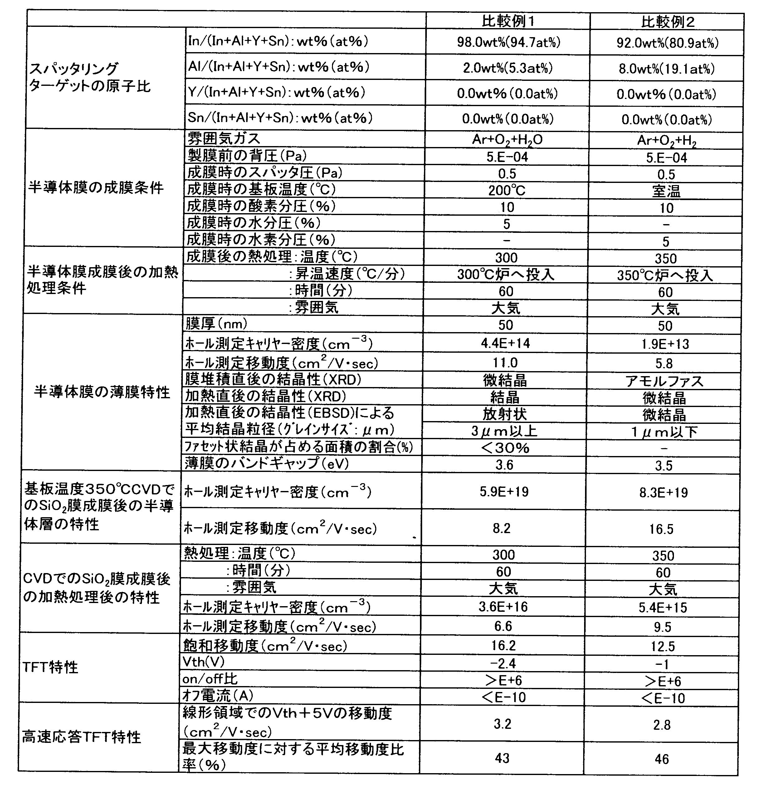
表2に示す組成のスパッタリングターゲットを用いて半導体薄膜を成膜し、加熱処理等を行った以外は実施例1と同様にして薄膜トランジスタを製造し、TFTの特性を評価した。
また、実施例1と同様に、酸化物薄膜のみをガラス基板に載せたサンプルについて、表2に示す各段階でホール測定を行い、キャリヤー密度の増減、バンドギャップを測定した。結果を表2に示す。
尚、表中のスパッタリングターゲットの原子比において、「wt%」で示されている数値は、酸化インジウム、酸化ガリウム、酸化イットリウム及び酸化錫の重量比(仕込み量)を示し、「at%」で示されている数値は、インジウム元素、ガリウム元素、イットリウム元素及びスズ元素の原子比を示す。
表中の「E+XX」は「1×10+XX」を意味する。
表中の「最大移動度に対する平均移動度比率(%)」は、Vg=VthからVth+20の範囲の最大移動度に対する、当該範囲における平均移動度の割合(%)を示す。

表3に示す組成のスパッタリングターゲットを用いて半導体薄膜を成膜し、加熱処理等を行った以外は実施例1と同様にして薄膜トランジスタを製造し、TFTの特性を評価した。
また、実施例1と同様に、酸化物薄膜のみをガラス基板に載せたサンプルについて、表3に示す各段階でホール測定を行い、キャリヤー密度の増減、バンドギャップを測定した。結果を表3に示す。
尚、表中のスパッタリングターゲットの原子比において、「wt%」で示されている数値は、酸化インジウム、酸化ガリウム、酸化サマリウム及び酸化錫の重量比(仕込み量)を示し、「at%」で示されている数値は、インジウム元素、ガリウム元素、サマリウム元素及びスズ元素の原子比を示す。
表中の「E+XX」は「1×10+XX」を意味する。
表中の「最大移動度に対する平均移動度比率(%)」は、Vg=VthからVth+20の範囲の最大移動度に対する、当該範囲における平均移動度の割合(%)を示す。

本願のパリ優先の基礎となる日本出願明細書の内容を全てここに援用する。
Claims (20)
- 酸化インジウムを主成分とし、単一の結晶方位を有する表面結晶粒子を含むことを特徴とする結晶質酸化物半導体薄膜。
- 電子線後方散乱解析法で観察したときに、表面の結晶状態がファセット状である結晶粒子が観察されることを特徴とする、請求項1に記載の結晶質酸化物半導体薄膜。
- 前記表面の結晶状態がファセット状である結晶粒子が占める面積が50%以上であることを特徴とする、請求項1又は2に記載の結晶質酸化物半導体薄膜。
- インジウム元素以外の正三価の金属元素からなる群から選択される1種以上の元素を含むことを特徴とする、請求項1~3のいずれかに記載の結晶質酸化物半導体薄膜。
- 前記インジウム元素以外の正三価の金属元素の含有量が、前記結晶質酸化物半導体薄膜中の全金属分に対し、8原子%超17原子%以下であることを特徴とする、請求項4に記載の結晶質酸化物半導体薄膜。
- 前記インジウム元素以外の正三価の金属元素が、アルミニウム、ガリウム、イットリウム及びランタノイド系元素からなる群から選択される1種又は2種以上であることを特徴とする、請求項4又は5に記載の結晶質酸化物半導体薄膜。
- さらに、正四価の金属元素からなる群から選択される1種以上の元素を含むことを特徴とする、請求項1~6のいずれかに記載の結晶質酸化物半導体薄膜。
- 前記正四価の金属元素の含有量が、前記結晶質酸化物半導体薄膜中の全金属分に対し、0.01原子%以上1原子%以下であることを特徴とする、請求項7に記載の結晶質酸化物半導体薄膜。
- 前記正四価の金属元素が、スズ、ジルコニウム及びセリウムからなる群から選択される1種以上であることを特徴とする、請求項7又は8に記載の結晶質酸化物半導体薄膜。
- バンドギャップが、3.6eV以上であることを特徴とする、請求項1~9のいずれかに記載の結晶質酸化物半導体薄膜。
- 酸化インジウムを主成分とするスパッタリングターゲットを用い、不純物ガスを実質的に含まないアルゴン及び酸素の混合ガスをスパッタガスとして用いてスパッタリングにより酸化物薄膜を成膜する工程、及び
得られた酸化物薄膜を加熱する工程
を含むことを特徴とする、請求項1~10のいずれかに記載の結晶質酸化物半導体薄膜の製造方法。 - 前記スパッタガス中の不純物ガスの割合が、0.1体積%以下であることを特徴とする、請求項11に記載の結晶質酸化物半導体薄膜の製造方法。
- 前記スパッタリングターゲットが、アルミニウム、ガリウム、イットリウム及びランタノイド系元素からなる群から選択される1種以上の元素を含有することを特徴とする、請求項11又は12に記載の結晶質酸化物半導体薄膜の製造方法。
- 前記加熱温度が、250℃以上500℃以下であることを特徴とする、請求項11~13のいずれかに記載の結晶質酸化物半導体薄膜の製造方法。
- 前記加熱する工程において、150℃から250℃までの昇温速度が、20℃/分以下であることを特徴とする、請求項11~14のいずれかに記載の結晶質酸化物半導体薄膜の製造方法。
- 前記加熱時間が、0.1時間以上5時間以下であることを特徴とする、請求項11~14のいずれかに記載の結晶質酸化物半導体薄膜の製造方法。
- ソース電極及びドレイン電極と、ゲート電極と、ゲート絶縁膜と、保護絶縁膜と、酸化物半導体層と、を有し、
前記酸化物半導体層は、ゲート絶縁膜と保護絶縁膜の間に位置し、請求項1~10のいずれかに記載の結晶質酸化物半導体薄膜からなることを特徴とする薄膜トランジスタ。 - 飽和移動度が30cm2/V・sec以上である、請求項17に記載の薄膜トランジスタ。
- ドレイン電圧0.1Vにおいて、線形領域での電界効果移動度の方法で求めたVg-μカーブより、Vg=Vth+5の移動度が10cm2/Vs以上であり、Vg=VthからVth+20の平均移動度がその範囲の最大移動度の50%以上であることを特徴とする請求項17又は18に記載の薄膜トランジスタ。
- 請求項17~19のいずれかに記載の薄膜トランジスタを用いた電気機器又は車両。
Priority Applications (4)
| Application Number | Priority Date | Filing Date | Title |
|---|---|---|---|
| JP2016573622A JP6097458B1 (ja) | 2015-07-30 | 2016-07-29 | 結晶質酸化物半導体薄膜、結晶質酸化物半導体薄膜の製造方法及び薄膜トランジスタ |
| CN201680044317.2A CN107924822B (zh) | 2015-07-30 | 2016-07-29 | 晶体氧化物半导体薄膜、晶体氧化物半导体薄膜的制造方法以及薄膜晶体管 |
| KR1020177034668A KR102530123B1 (ko) | 2015-07-30 | 2016-07-29 | 결정질 산화물 반도체 박막, 결정질 산화물 반도체 박막의 제조 방법 및 박막 트랜지스터 |
| US15/748,356 US10636914B2 (en) | 2015-07-30 | 2016-07-29 | Crystalline oxide semiconductor thin film, method for producing crystalline oxide semiconductor thin film, and thin film transistor |
Applications Claiming Priority (2)
| Application Number | Priority Date | Filing Date | Title |
|---|---|---|---|
| JP2015-150701 | 2015-07-30 | ||
| JP2015150701 | 2015-07-30 |
Publications (1)
| Publication Number | Publication Date |
|---|---|
| WO2017017966A1 true WO2017017966A1 (ja) | 2017-02-02 |
Family
ID=57885117
Family Applications (1)
| Application Number | Title | Priority Date | Filing Date |
|---|---|---|---|
| PCT/JP2016/003528 Ceased WO2017017966A1 (ja) | 2015-07-30 | 2016-07-29 | 結晶質酸化物半導体薄膜、結晶質酸化物半導体薄膜の製造方法及び薄膜トランジスタ |
Country Status (6)
| Country | Link |
|---|---|
| US (1) | US10636914B2 (ja) |
| JP (3) | JP6097458B1 (ja) |
| KR (1) | KR102530123B1 (ja) |
| CN (1) | CN107924822B (ja) |
| TW (1) | TWI706925B (ja) |
| WO (1) | WO2017017966A1 (ja) |
Cited By (7)
| Publication number | Priority date | Publication date | Assignee | Title |
|---|---|---|---|---|
| WO2018143073A1 (ja) * | 2017-02-01 | 2018-08-09 | 出光興産株式会社 | 結晶質酸化物半導体薄膜、積層体の製造方法、薄膜トランジスタ、薄膜トランジスタの製造方法、電子機器、車載用表示装置 |
| WO2018181716A1 (ja) * | 2017-03-30 | 2018-10-04 | 出光興産株式会社 | ガーネット化合物、酸化物焼結体、酸化物半導体薄膜、薄膜トランジスタ、電子機器、およびイメージセンサー |
| JP2019057622A (ja) * | 2017-09-21 | 2019-04-11 | 株式会社東芝 | 半導体装置 |
| WO2020196716A1 (ja) * | 2019-03-28 | 2020-10-01 | 出光興産株式会社 | 結晶酸化物薄膜、積層体及び薄膜トランジスタ |
| WO2023063348A1 (ja) * | 2021-10-14 | 2023-04-20 | 出光興産株式会社 | 結晶酸化物薄膜、積層体及び薄膜トランジスタ |
| WO2026014186A1 (ja) * | 2024-07-10 | 2026-01-15 | 株式会社コベルコ科研 | 酸化物半導体薄膜、複合薄膜およびスパッタリングターゲット |
| JP2026012042A (ja) * | 2024-07-10 | 2026-01-23 | 株式会社コベルコ科研 | 酸化物半導体薄膜、複合薄膜およびスパッタリングターゲット |
Families Citing this family (5)
| Publication number | Priority date | Publication date | Assignee | Title |
|---|---|---|---|---|
| CN110234785B (zh) * | 2017-02-01 | 2022-05-24 | 出光兴产株式会社 | 非晶质氧化物半导体膜、氧化物烧结体以及薄膜晶体管 |
| CN116240630A (zh) * | 2018-08-01 | 2023-06-09 | 出光兴产株式会社 | 晶体化合物、氧化物烧结体、溅射靶、晶质及无定形氧化物薄膜、薄膜晶体管及电子设备 |
| US11760650B2 (en) * | 2018-08-01 | 2023-09-19 | Idemitsu Kosan Co.,Ltd. | Compound |
| JPWO2021106811A1 (ja) * | 2019-11-29 | 2021-06-03 | ||
| KR102944064B1 (ko) * | 2022-03-30 | 2026-03-27 | 가부시키가이샤 재팬 디스프레이 | 박막 트랜지스터 및 전자 기기 |
Citations (5)
| Publication number | Priority date | Publication date | Assignee | Title |
|---|---|---|---|---|
| JP2012169344A (ja) * | 2011-02-10 | 2012-09-06 | Sony Corp | 薄膜トランジスタならびに表示装置および電子機器 |
| JP2012253315A (ja) * | 2010-12-28 | 2012-12-20 | Idemitsu Kosan Co Ltd | 酸化物半導体薄膜層を有する積層構造及び薄膜トランジスタ |
| US20130108877A1 (en) * | 2011-09-12 | 2013-05-02 | Tom E. Blomberg | Crystalline strontium titanate and methods of forming the same |
| JP2013144841A (ja) * | 2011-06-08 | 2013-07-25 | Semiconductor Energy Lab Co Ltd | ターゲット、ターゲットの使用方法、及び半導体装置の作製方法 |
| JP2015018959A (ja) * | 2013-07-11 | 2015-01-29 | 出光興産株式会社 | 酸化物半導体及び酸化物半導体膜の製造方法 |
Family Cites Families (18)
| Publication number | Priority date | Publication date | Assignee | Title |
|---|---|---|---|---|
| EP1950177A4 (en) * | 2005-11-18 | 2009-02-25 | Idemitsu Kosan Co | SEMICONDUCTOR THIN FILM, MANUFACTURING METHOD AND THIN FILM TRANSISTOR |
| JP5244327B2 (ja) | 2007-03-05 | 2013-07-24 | 出光興産株式会社 | スパッタリングターゲット |
| EP2471972B1 (en) | 2006-12-13 | 2014-01-29 | Idemitsu Kosan Co., Ltd. | Sputtering target |
| JP5237558B2 (ja) | 2007-01-05 | 2013-07-17 | 出光興産株式会社 | スパッタリングターゲット及び酸化物半導体膜 |
| JP5237557B2 (ja) | 2007-01-05 | 2013-07-17 | 出光興産株式会社 | スパッタリングターゲット及びその製造方法 |
| US9269573B2 (en) * | 2008-09-17 | 2016-02-23 | Idemitsu Kosan Co., Ltd. | Thin film transistor having crystalline indium oxide semiconductor film |
| CN103204674A (zh) | 2008-12-15 | 2013-07-17 | 出光兴产株式会社 | 氧化铟系烧结体及溅射靶 |
| KR20100070944A (ko) | 2008-12-18 | 2010-06-28 | 배경환 | 밝기 조절 스탠드 |
| JP5491258B2 (ja) | 2010-04-02 | 2014-05-14 | 出光興産株式会社 | 酸化物半導体の成膜方法 |
| JP5689250B2 (ja) | 2010-05-27 | 2015-03-25 | 出光興産株式会社 | 酸化物焼結体、それからなるターゲット及び酸化物半導体薄膜 |
| JP2012144410A (ja) | 2011-01-14 | 2012-08-02 | Kobelco Kaken:Kk | 酸化物焼結体およびスパッタリングターゲット |
| KR20120090490A (ko) | 2011-02-08 | 2012-08-17 | 주식회사 지.엠 | 기판 검사장치 |
| WO2013021632A1 (ja) * | 2011-08-11 | 2013-02-14 | 出光興産株式会社 | 薄膜トランジスタ |
| JP5301021B2 (ja) * | 2011-09-06 | 2013-09-25 | 出光興産株式会社 | スパッタリングターゲット |
| JP5966840B2 (ja) * | 2012-10-11 | 2016-08-10 | 住友金属鉱山株式会社 | 酸化物半導体薄膜および薄膜トランジスタ |
| US9455349B2 (en) * | 2013-10-22 | 2016-09-27 | Semiconductor Energy Laboratory Co., Ltd. | Oxide semiconductor thin film transistor with reduced impurity diffusion |
| JP2015109315A (ja) * | 2013-12-03 | 2015-06-11 | 出光興産株式会社 | 薄膜トランジスタ、その製造方法、酸化物半導体層、表示装置及び半導体装置 |
| CN105873881A (zh) * | 2013-12-27 | 2016-08-17 | 出光兴产株式会社 | 氧化物烧结体、该烧结体的制造方法及溅射靶 |
-
2016
- 2016-07-29 WO PCT/JP2016/003528 patent/WO2017017966A1/ja not_active Ceased
- 2016-07-29 US US15/748,356 patent/US10636914B2/en active Active
- 2016-07-29 KR KR1020177034668A patent/KR102530123B1/ko active Active
- 2016-07-29 CN CN201680044317.2A patent/CN107924822B/zh active Active
- 2016-07-29 JP JP2016573622A patent/JP6097458B1/ja active Active
- 2016-08-01 TW TW105124350A patent/TWI706925B/zh active
-
2017
- 2017-02-15 JP JP2017025807A patent/JP6289693B2/ja active Active
-
2018
- 2018-02-05 JP JP2018017996A patent/JP2018101793A/ja active Pending
Patent Citations (5)
| Publication number | Priority date | Publication date | Assignee | Title |
|---|---|---|---|---|
| JP2012253315A (ja) * | 2010-12-28 | 2012-12-20 | Idemitsu Kosan Co Ltd | 酸化物半導体薄膜層を有する積層構造及び薄膜トランジスタ |
| JP2012169344A (ja) * | 2011-02-10 | 2012-09-06 | Sony Corp | 薄膜トランジスタならびに表示装置および電子機器 |
| JP2013144841A (ja) * | 2011-06-08 | 2013-07-25 | Semiconductor Energy Lab Co Ltd | ターゲット、ターゲットの使用方法、及び半導体装置の作製方法 |
| US20130108877A1 (en) * | 2011-09-12 | 2013-05-02 | Tom E. Blomberg | Crystalline strontium titanate and methods of forming the same |
| JP2015018959A (ja) * | 2013-07-11 | 2015-01-29 | 出光興産株式会社 | 酸化物半導体及び酸化物半導体膜の製造方法 |
Non-Patent Citations (1)
| Title |
|---|
| EBATA,KAZUAKI: "High-Mobility Thin-Film Transistors with Polycrystalline In-Ga-O Channel Fabricated by DC Magnetron Sputtering", APPLIED PHYSICS EXPRESS, vol. APEX.5.0, 2012, pages 1 - 3, XP001576505 * |
Cited By (17)
| Publication number | Priority date | Publication date | Assignee | Title |
|---|---|---|---|---|
| WO2018143073A1 (ja) * | 2017-02-01 | 2018-08-09 | 出光興産株式会社 | 結晶質酸化物半導体薄膜、積層体の製造方法、薄膜トランジスタ、薄膜トランジスタの製造方法、電子機器、車載用表示装置 |
| US11447421B2 (en) | 2017-03-30 | 2022-09-20 | Idemitsu Kosan Co., Ltd. | Garnet compound, oxide sintered compact, oxide semiconductor thin film, thin film transistor, electronic device and image sensor |
| JP7092746B2 (ja) | 2017-03-30 | 2022-06-28 | 出光興産株式会社 | 酸化物焼結体、スパッタリングターゲット、酸化物半導体薄膜、薄膜トランジスタ、および電子機器 |
| CN110678433A (zh) * | 2017-03-30 | 2020-01-10 | 出光兴产株式会社 | 石榴石化合物、氧化物烧结体、氧化物半导体薄膜、薄膜晶体管、电子设备以及图像传感器 |
| JPWO2018181716A1 (ja) * | 2017-03-30 | 2020-05-14 | 出光興産株式会社 | ガーネット化合物、酸化物焼結体、酸化物半導体薄膜、薄膜トランジスタ、電子機器、およびイメージセンサー |
| WO2018181716A1 (ja) * | 2017-03-30 | 2018-10-04 | 出光興産株式会社 | ガーネット化合物、酸化物焼結体、酸化物半導体薄膜、薄膜トランジスタ、電子機器、およびイメージセンサー |
| US11075305B2 (en) | 2017-09-21 | 2021-07-27 | Kabushiki Kaisha Toshiba | Semiconductor device |
| JP2019057622A (ja) * | 2017-09-21 | 2019-04-11 | 株式会社東芝 | 半導体装置 |
| WO2020196716A1 (ja) * | 2019-03-28 | 2020-10-01 | 出光興産株式会社 | 結晶酸化物薄膜、積層体及び薄膜トランジスタ |
| KR20210144707A (ko) * | 2019-03-28 | 2021-11-30 | 이데미쓰 고산 가부시키가이샤 | 결정 산화물 박막, 적층체 및 박막 트랜지스터 |
| JP6853421B2 (ja) * | 2019-03-28 | 2021-03-31 | 出光興産株式会社 | 結晶酸化物薄膜、積層体及び薄膜トランジスタ |
| KR102428977B1 (ko) | 2019-03-28 | 2022-08-03 | 이데미쓰 고산 가부시키가이샤 | 결정 산화물 박막, 적층체 및 박막 트랜지스터 |
| JPWO2020196716A1 (ja) * | 2019-03-28 | 2021-04-08 | 出光興産株式会社 | 結晶酸化物薄膜、積層体及び薄膜トランジスタ |
| US12205992B2 (en) | 2019-03-28 | 2025-01-21 | Idemitsu Kosan Co., Ltd. | Crystalline oxide thin film, multilayer body and thin film transistor |
| WO2023063348A1 (ja) * | 2021-10-14 | 2023-04-20 | 出光興産株式会社 | 結晶酸化物薄膜、積層体及び薄膜トランジスタ |
| WO2026014186A1 (ja) * | 2024-07-10 | 2026-01-15 | 株式会社コベルコ科研 | 酸化物半導体薄膜、複合薄膜およびスパッタリングターゲット |
| JP2026012042A (ja) * | 2024-07-10 | 2026-01-23 | 株式会社コベルコ科研 | 酸化物半導体薄膜、複合薄膜およびスパッタリングターゲット |
Also Published As
| Publication number | Publication date |
|---|---|
| JP6097458B1 (ja) | 2017-03-15 |
| JPWO2017017966A1 (ja) | 2017-07-27 |
| KR20180034318A (ko) | 2018-04-04 |
| CN107924822A (zh) | 2018-04-17 |
| CN107924822B (zh) | 2022-10-28 |
| KR102530123B1 (ko) | 2023-05-08 |
| JP2017123472A (ja) | 2017-07-13 |
| JP6289693B2 (ja) | 2018-03-07 |
| US10636914B2 (en) | 2020-04-28 |
| US20180219098A1 (en) | 2018-08-02 |
| JP2018101793A (ja) | 2018-06-28 |
| TWI706925B (zh) | 2020-10-11 |
| TW201714854A (zh) | 2017-05-01 |
Similar Documents
| Publication | Publication Date | Title |
|---|---|---|
| JP6289693B2 (ja) | 結晶質酸化物半導体薄膜、結晶質酸化物半導体薄膜の製造方法及び薄膜トランジスタ | |
| JP7187322B2 (ja) | 結晶質酸化物半導体薄膜、積層体の製造方法、薄膜トランジスタ、薄膜トランジスタの製造方法、電子機器、車載用表示装置 | |
| KR100939998B1 (ko) | 비정질 산화물 및 전계 효과 트랜지스터 | |
| JP5966840B2 (ja) | 酸化物半導体薄膜および薄膜トランジスタ | |
| JP6376153B2 (ja) | 酸化物半導体薄膜および薄膜トランジスタ | |
| WO2013021632A1 (ja) | 薄膜トランジスタ | |
| JP6107085B2 (ja) | 酸化物半導体薄膜および薄膜トランジスタ | |
| WO2012121332A1 (ja) | 薄膜トランジスタの半導体層用酸化物、上記酸化物を備えた薄膜トランジスタの半導体層および薄膜トランジスタ | |
| WO2014061638A1 (ja) | 薄膜トランジスタ | |
| JP6143423B2 (ja) | 半導体装置の製造方法 | |
| TWI601214B (zh) | 氧氮化物半導體薄膜與其製造方法,及薄膜電晶體 | |
| JP2016201458A (ja) | 微結晶質酸化物半導体薄膜及びそれを用いた薄膜トランジスタ |
Legal Events
| Date | Code | Title | Description |
|---|---|---|---|
| ENP | Entry into the national phase |
Ref document number: 2016573622 Country of ref document: JP Kind code of ref document: A |
|
| 121 | Ep: the epo has been informed by wipo that ep was designated in this application |
Ref document number: 16830071 Country of ref document: EP Kind code of ref document: A1 |
|
| ENP | Entry into the national phase |
Ref document number: 20177034668 Country of ref document: KR Kind code of ref document: A |
|
| WWE | Wipo information: entry into national phase |
Ref document number: 15748356 Country of ref document: US |
|
| NENP | Non-entry into the national phase |
Ref country code: DE |
|
| 122 | Ep: pct application non-entry in european phase |
Ref document number: 16830071 Country of ref document: EP Kind code of ref document: A1 |