WO2017086424A1 - 光電変換素子 - Google Patents
光電変換素子 Download PDFInfo
- Publication number
- WO2017086424A1 WO2017086424A1 PCT/JP2016/084215 JP2016084215W WO2017086424A1 WO 2017086424 A1 WO2017086424 A1 WO 2017086424A1 JP 2016084215 W JP2016084215 W JP 2016084215W WO 2017086424 A1 WO2017086424 A1 WO 2017086424A1
- Authority
- WO
- WIPO (PCT)
- Prior art keywords
- photoelectric conversion
- transparent conductive
- layer
- insulating layer
- conversion element
- Prior art date
- Legal status (The legal status is an assumption and is not a legal conclusion. Google has not performed a legal analysis and makes no representation as to the accuracy of the status listed.)
- Ceased
Links
Images


Classifications
-
- H—ELECTRICITY
- H01—ELECTRIC ELEMENTS
- H01G—CAPACITORS; CAPACITORS, RECTIFIERS, DETECTORS, SWITCHING DEVICES, LIGHT-SENSITIVE OR TEMPERATURE-SENSITIVE DEVICES OF THE ELECTROLYTIC TYPE
- H01G9/00—Electrolytic capacitors, rectifiers, detectors, switching devices, light-sensitive or temperature-sensitive devices; Processes of their manufacture
- H01G9/20—Light-sensitive devices
- H01G9/2068—Panels or arrays of photoelectrochemical cells, e.g. photovoltaic modules based on photoelectrochemical cells
- H01G9/2077—Sealing arrangements, e.g. to prevent the leakage of the electrolyte
-
- H—ELECTRICITY
- H01—ELECTRIC ELEMENTS
- H01G—CAPACITORS; CAPACITORS, RECTIFIERS, DETECTORS, SWITCHING DEVICES, LIGHT-SENSITIVE OR TEMPERATURE-SENSITIVE DEVICES OF THE ELECTROLYTIC TYPE
- H01G9/00—Electrolytic capacitors, rectifiers, detectors, switching devices, light-sensitive or temperature-sensitive devices; Processes of their manufacture
- H01G9/20—Light-sensitive devices
- H01G9/2068—Panels or arrays of photoelectrochemical cells, e.g. photovoltaic modules based on photoelectrochemical cells
- H01G9/2081—Serial interconnection of cells
-
- H—ELECTRICITY
- H10—SEMICONDUCTOR DEVICES; ELECTRIC SOLID-STATE DEVICES NOT OTHERWISE PROVIDED FOR
- H10K—ORGANIC ELECTRIC SOLID-STATE DEVICES
- H10K30/00—Organic devices sensitive to infrared radiation, light, electromagnetic radiation of shorter wavelength or corpuscular radiation
- H10K30/80—Constructional details
- H10K30/81—Electrodes
-
- H—ELECTRICITY
- H10—SEMICONDUCTOR DEVICES; ELECTRIC SOLID-STATE DEVICES NOT OTHERWISE PROVIDED FOR
- H10K—ORGANIC ELECTRIC SOLID-STATE DEVICES
- H10K30/00—Organic devices sensitive to infrared radiation, light, electromagnetic radiation of shorter wavelength or corpuscular radiation
- H10K30/80—Constructional details
- H10K30/88—Passivation; Containers; Encapsulations
-
- H—ELECTRICITY
- H10—SEMICONDUCTOR DEVICES; ELECTRIC SOLID-STATE DEVICES NOT OTHERWISE PROVIDED FOR
- H10K—ORGANIC ELECTRIC SOLID-STATE DEVICES
- H10K39/00—Integrated devices, or assemblies of multiple devices, comprising at least one organic radiation-sensitive element covered by group H10K30/00
- H10K39/10—Organic photovoltaic [PV] modules; Arrays of single organic PV cells
- H10K39/12—Electrical configurations of PV cells, e.g. series connections or parallel connections
-
- H—ELECTRICITY
- H01—ELECTRIC ELEMENTS
- H01G—CAPACITORS; CAPACITORS, RECTIFIERS, DETECTORS, SWITCHING DEVICES, LIGHT-SENSITIVE OR TEMPERATURE-SENSITIVE DEVICES OF THE ELECTROLYTIC TYPE
- H01G9/00—Electrolytic capacitors, rectifiers, detectors, switching devices, light-sensitive or temperature-sensitive devices; Processes of their manufacture
- H01G9/20—Light-sensitive devices
- H01G9/2027—Light-sensitive devices comprising an oxide semiconductor electrode
- H01G9/2031—Light-sensitive devices comprising an oxide semiconductor electrode comprising titanium oxide, e.g. TiO2
-
- H—ELECTRICITY
- H01—ELECTRIC ELEMENTS
- H01G—CAPACITORS; CAPACITORS, RECTIFIERS, DETECTORS, SWITCHING DEVICES, LIGHT-SENSITIVE OR TEMPERATURE-SENSITIVE DEVICES OF THE ELECTROLYTIC TYPE
- H01G9/00—Electrolytic capacitors, rectifiers, detectors, switching devices, light-sensitive or temperature-sensitive devices; Processes of their manufacture
- H01G9/20—Light-sensitive devices
- H01G9/2059—Light-sensitive devices comprising an organic dye as the active light absorbing material, e.g. adsorbed on an electrode or dissolved in solution
-
- Y—GENERAL TAGGING OF NEW TECHNOLOGICAL DEVELOPMENTS; GENERAL TAGGING OF CROSS-SECTIONAL TECHNOLOGIES SPANNING OVER SEVERAL SECTIONS OF THE IPC; TECHNICAL SUBJECTS COVERED BY FORMER USPC CROSS-REFERENCE ART COLLECTIONS [XRACs] AND DIGESTS
- Y02—TECHNOLOGIES OR APPLICATIONS FOR MITIGATION OR ADAPTATION AGAINST CLIMATE CHANGE
- Y02E—REDUCTION OF GREENHOUSE GAS [GHG] EMISSIONS, RELATED TO ENERGY GENERATION, TRANSMISSION OR DISTRIBUTION
- Y02E10/00—Energy generation through renewable energy sources
- Y02E10/50—Photovoltaic [PV] energy
- Y02E10/542—Dye sensitized solar cells
-
- Y—GENERAL TAGGING OF NEW TECHNOLOGICAL DEVELOPMENTS; GENERAL TAGGING OF CROSS-SECTIONAL TECHNOLOGIES SPANNING OVER SEVERAL SECTIONS OF THE IPC; TECHNICAL SUBJECTS COVERED BY FORMER USPC CROSS-REFERENCE ART COLLECTIONS [XRACs] AND DIGESTS
- Y02—TECHNOLOGIES OR APPLICATIONS FOR MITIGATION OR ADAPTATION AGAINST CLIMATE CHANGE
- Y02E—REDUCTION OF GREENHOUSE GAS [GHG] EMISSIONS, RELATED TO ENERGY GENERATION, TRANSMISSION OR DISTRIBUTION
- Y02E10/00—Energy generation through renewable energy sources
- Y02E10/50—Photovoltaic [PV] energy
- Y02E10/549—Organic PV cells
Definitions
- the present invention relates to a photoelectric conversion element.
- a photoelectric conversion element using a dye is attracting attention because it is inexpensive and can provide high photoelectric conversion efficiency.
- This dye-sensitized solar cell element includes a substrate and at least one photoelectric conversion cell, and the photoelectric conversion cell is opposed to the first transparent conductive layer provided on the substrate and the first transparent conductive layer.
- the substrate includes an annular sealing portion that joins the first transparent conductive layer and the counter substrate.
- a second transparent conductive layer is provided on the substrate and outside the first transparent conductive layer, and a groove is formed between the second transparent conductive layer and the first transparent conductive layer. .
- an insulating material enters a groove extending outside the sealing portion, and this insulating material covers a part of the second transparent conductive layer.
- the dye-sensitized solar cell element described in Patent Document 1 when the dye-sensitized solar cell element is viewed from a direction orthogonal to one surface of the substrate, the first transparent layer is between the sealing portion and the insulating material. There is a portion where the conductive layer is exposed, and no polarization occurs in the first transparent conductive layer. For this reason, the dye-sensitized solar cell element described in Patent Document 1 can suppress charging, and can sufficiently suppress adverse effects on peripheral devices due to this charging. However, the dye-sensitized solar cell element described in Patent Document 1 has room for improvement in terms of durability.
- the present invention has been made in view of the above circumstances, and an object thereof is to provide a photoelectric conversion element having excellent durability while suppressing charging.
- the present inventors diligently studied to solve the above problems.
- the insulating material enters a groove extending outside the sealing portion of the photoelectric conversion cell, but the photoelectric conversion element is orthogonal to one surface of the substrate.
- part of the first transparent conductive layer and part of the second transparent conductive layer are exposed.
- all of the exposed portions of the first transparent conductive layer and the second transparent conductive layer may be covered with an insulating material.
- charging cannot be sufficiently suppressed.
- the present inventors have found that the above-described problems can be solved by the following invention.
- the present invention includes a first substrate and a conductive layer provided on one surface of the first substrate, and the conductive layer includes a first conductive layer having at least one first conductive portion; A photoelectric conversion element provided outside the one conductive layer and having a second conductive layer having at least one second conductive portion, the photoelectric conversion element having at least one photoelectric conversion cell, wherein the photoelectric conversion cell is A first conductive layer; a second substrate facing the first conductive portion; and an annular sealing portion that joins the first substrate and the second substrate; and the first conductive layer and the second conductive
- the layer is disposed via a first groove, the photoelectric conversion element has an insulating layer, and the insulating layer is between the sealing portion of the at least one photoelectric conversion cell and the first substrate.
- the outer peripheral edge of the insulating layer is provided so as to overlap the sealing portion, and the photoelectric conversion element When viewed from a direction perpendicular to the one surface of the first substrate, the outer periphery of the sealing portion and the entire sealing portion of the at least one photoelectric conversion cell are surrounded,
- An insulating layer covers and conceals a portion of the first conductive layer that is outside the sealing portion inside the outer peripheral edge of the insulating layer and outside the sealing portion, and is formed in the first groove. It is a photoelectric conversion element which penetrates and covers a part of the second conductive layer, and the remaining part of the second conductive layer is exposed.
- This photoelectric conversion element can have excellent durability while suppressing charging.
- the present inventors guess as follows about the reason why charging can be suppressed by the photoelectric conversion element of the present invention. That is, a part of the second conductive layer provided outside the first conductive part included in at least one photoelectric conversion cell is covered with the insulating layer, and the remaining part of the second conductive layer is exposed. For this reason, there is no charge in the remaining part of the second conductive layer, and further, charging to the insulating layer is suppressed. For this reason, the charge to a photoelectric conversion element is fully suppressed. From the above, the present inventors speculate that charging can be suppressed according to the photoelectric conversion element of the present invention.
- the present inventors infer the reason why the photoelectric conversion element of the present invention can have excellent durability as follows. That is, in the photoelectric conversion element of the present invention, when the photoelectric conversion element is viewed from a direction orthogonal to one surface of the first substrate, the entire sealing portion in at least one photoelectric conversion cell is surrounded outside the sealing portion. Is provided with an outer peripheral edge of the insulating layer, and the insulating layer covers a portion of the first conductive layer that protrudes outside the sealing portion inside the outer peripheral edge of the insulating layer and outside the sealing portion. Hidden. For this reason, it is sufficiently suppressed that moisture enters inside the outer peripheral edge of the insulating layer.
- the insulating layer lengthens the moisture path from the interface between the second conductive layer and the insulating layer to the photoelectric conversion cell. Furthermore, an insulating layer enters the first groove. For this reason, the penetration
- the end of the first groove may reach the outer peripheral edge of the conductive layer, and the insulating layer may also enter the end of the first groove.
- the insulating layer since the insulating layer also enters the end of the first groove, moisture can be sufficiently prevented from entering the photoelectric conversion cell through the end of the first groove.
- the at least one photoelectric conversion cell includes a plurality of the photoelectric conversion cells, and the first conductive layer has the same number of the first conversion cells as the photoelectric conversion cells. It is preferable that a second groove that separates the adjacent first conductive parts is formed so as to form a conductive part, and the insulating layer also enters the second groove.
- the insulating layer also enters the second groove formed in the first conductive layer, moisture can be sufficiently suppressed from entering the plurality of photoelectric conversion cells through the second groove.
- the insulating layer penetrates all of the first groove.
- the durability of the photoelectric conversion element 100 can be further improved.
- the width at the portion where the width between the outer peripheral edge of the second conductive portion and the first groove is maximum is Wmax, and the width at which the second conductive portion is exposed is W1.
- W1 / Wmax is preferably 0.1 or more.
- the durability of the photoelectric conversion element can be further improved, and charging to the photoelectric conversion element can be more sufficiently suppressed.
- the insulating layer covers and covers the entire portion of the first conductive layer that is outside the sealing portion outside the sealing portion.
- the photoelectric conversion characteristics of the photoelectric conversion element can be further improved.
- a photoelectric conversion element having excellent durability while suppressing charging is provided.
- FIGS. 1 is a cross-sectional view showing a first embodiment of the photoelectric conversion element of the present invention
- FIG. 2 is a plan view showing the first embodiment of the photoelectric conversion element of the present invention
- FIG. 3 is a photoelectric conversion element of FIG.
- FIG. 4 is a plan view showing the first integrated sealing portion of FIG. 1
- FIG. 5 is a plan view showing the second integrated sealing portion of FIG. 1
- FIG. FIG. 3 is a plan view showing a part of the photoelectric conversion element of FIG. 2.
- the photoelectric conversion element 100 includes a transparent substrate 11 as a first substrate and a conductive substrate having a transparent conductive layer 112 as a conductive layer provided on one surface 11 a of the transparent substrate 11. 15 is provided.
- the transparent conductive layer 112 includes a first transparent conductive layer 112X having a first transparent conductive portion 12E and a plurality of (four in FIG. 3) first transparent conductive portions 12A to 12D as first conductive portions, A second transparent conductive layer 112Y provided on the outside of the transparent conductive layer 112X and having a second transparent conductive portion 12F as at least one (one in FIG. 3) second conductive portion.
- FIG. 1 the photoelectric conversion element 100 includes a transparent substrate 11 as a first substrate and a conductive substrate having a transparent conductive layer 112 as a conductive layer provided on one surface 11 a of the transparent substrate 11. 15 is provided.
- the transparent conductive layer 112 includes a first transparent conductive layer 112X having a first transparent conductive portion 12E and a
- the first transparent conductive layer 112X is a transparent conductive layer in a region surrounded by a two-dot chain line.
- the first transparent conductive layer 112X constitutes a first conductive layer
- the second transparent conductive layer 112Y constitutes a second conductive layer.
- the first transparent conductive layer 112X and the second transparent conductive layer 112Y are disposed via the first groove 90A.
- the first transparent conductive layer 112X includes a plurality of first transparent conductive portions 12A to 12A together with the first groove 90A.
- a second groove 90B that separates adjacent first transparent conductive portions is formed so as to form 12D and the first transparent conductive portion 12E.
- the photoelectric conversion element 100 includes a plurality (four in FIG. 1) of photoelectric conversion cells (hereinafter sometimes simply referred to as “cells”) 50, and the plurality of cells 50 are connected in series by a wiring member 60P. (See FIG. 2).
- the four cells 50 in the photoelectric conversion element 100 may be referred to as cells 50A to 50D.
- Each of the plurality of cells 50 includes a first transparent conductive portion 12A, 12B, 12C, or 12D, at least one oxide semiconductor layer 13 provided on the first transparent conductive portion 12A, 12B, 12C, or 12D, and a first A counter electrode 20 as a second substrate facing the transparent conductive portion 12A, 12B, 12C or 12D and an annular sealing portion 30A for joining the transparent substrate 11 and the counter electrode 20 are provided.
- the oxide semiconductor layer 13 is disposed inside the annular sealing portion 30A.
- the oxide semiconductor layer 13 carries a dye.
- An electrolyte 40 is disposed between the first transparent conductive portion 12A, 12B, 12C, or 12D and the counter electrode 20, and the electrolyte 40 is surrounded by an annular sealing portion 30A.
- the counter electrode 20 includes a metal substrate 21 and a catalyst layer 22 that is provided on the first transparent conductive portion 12A, 12B, 12C, or 12D side of the metal substrate 21 and promotes a catalytic reaction. In two adjacent cells 50, the counter electrodes 20 are separated from each other. A desiccant 95 may be provided on the counter electrode 20 of each cell 50.
- the transparent substrate 11 is used as a common transparent substrate for the cells 50A to 50D.
- each of the first transparent conductive portions 12A to 12D has a rectangular main body portion 12a having a side edge portion 12b, and a protruding portion 12c protruding sideways from the side edge portion 12b of the main body portion 12a. And have.
- the shape of the main body portion 12a is not limited to a square shape, and may be various shapes.
- the projecting portion 12c of the first transparent conductive portion 12C extends from the overhanging portion 12d and the overhanging portion 12d that project to the side with respect to the arrangement direction X of the cells 50A to 50D.
- the main body portion 12a of the adjacent cell 50D has a facing portion 12e facing the second groove 90B.
- the protruding portion 12c of the first transparent conductive portion 12B has an overhang portion 12d and a facing portion 12e. Also in the cell 50A, the protruding portion 12c of the first transparent conductive portion 12A has an overhang portion 12d and a facing portion 12e.
- the cell 50D is already connected to the cell 50C, and there is no other cell 50 to be connected to the cell 50D. For this reason, in the cell 50D, the protruding portion 12c of the first transparent conductive portion 12D does not have the facing portion 12e. That is, the protruding portion 12c of the first transparent conductive portion 12D is configured only by the overhang portion 12d.
- the first transparent conductive portion 12D connects the first current extraction portion 12f for extracting the current generated in the photoelectric conversion element 100 to the outside, the first current extraction portion 12f, and the main body portion 12a, and the first transparent conductive portion 12D. And a connection portion 12g extending along the side edge portion 12b of the portions 12A to 12C.
- the first current extraction portion 12f is disposed on the opposite side of the first transparent conductive portion 12B with respect to the first transparent conductive portion 12A.
- the first transparent conductive portion 12E has a second current extraction portion 12h for extracting the current generated in the photoelectric conversion element 100 to the outside.
- the second current extraction portion 12h of the first transparent conductive portion 12E is
- the first transparent conductive portion 12A is disposed on the opposite side to the first transparent conductive portion 12B.
- the first current extraction portion 12f and the second current extraction portion 12h of the first transparent conductive portion 12E are arranged adjacent to each other via the second groove 90B.
- connection terminal 16 is provided on each protruding portion 12c of the first transparent conductive portions 12A to 12C and the first transparent conductive portion 12E.
- the connection terminal 16 includes a wiring material connection portion to which the wiring material 60P is connected and a wiring material non-connection portion to which the wiring material 60P is not connected.
- the sealing portion 30A has an annular first sealing portion 31A provided between the first transparent conductive portions 12A to 12D and the counter electrode 20.
- the adjacent first sealing portions 31A are integrated as shown in FIG. 4 to form a first integrated sealing portion 31.
- the first integrated sealing portion 31 includes an annular portion (hereinafter referred to as “annular portion”) 31 a that is not provided between two adjacent counter electrodes 20 and two adjacent counter electrodes 20.
- a portion 31b is provided between the inner opening 31c of the annular portion 31a.
- the adjacent first sealing portions 31A may not be integrated. Further, as shown in FIG.
- the sealing part 30A is provided so as to overlap the first sealing part 31A, and the annular second sealing part sandwiching the edge part 20a of the counter electrode 20 together with the first sealing part 31A.
- 32A may further be included.
- the second sealing portions 32 ⁇ / b> A are integrated between the adjacent counter electrodes 20 to constitute a second integrated sealing portion 32.
- the second integrated sealing portion 32 is provided between an annular portion (hereinafter referred to as “annular portion”) 32 a that is not provided between two adjacent counter electrodes 20 and two adjacent counter electrodes 20. And a portion 32b that partitions the inner opening 32c of the annular portion 32a.
- the adjacent second sealing portions 32A may not be integrated.
- the photoelectric conversion element 100 has an insulating layer 33 made of an insulating material. Between the first sealing portion 31A and the first transparent conductive portion 12A, 12B, 12C, or 12D, an insulating layer 33 is provided along the outer shape of the first sealing portion 31A. That is, the insulating layer 33 is provided between the sealing portion 30 ⁇ / b> A and the transparent substrate 11 so as to overlap the sealing portion 30 ⁇ / b> A between the sealing portion 30 ⁇ / b> A and the transparent substrate 11.
- the first transparent conductive layer 112X adjacent first transparent conductive portions are separated so as to form a plurality of first transparent conductive portions 12A to 12D and a first transparent conductive portion 12E together with the first groove 90A.
- a second groove 90B is formed.
- the insulating layer 33 also enters the second groove 90B.
- the insulating layer 33 may cover only a part of the first transparent conductive portion 12A to 12D excluding the interface with the oxide semiconductor layer 13 inside the annular first sealing portion 31A. It's okay, but you can cover everything. Note that when the insulating layer 33 covers the entire region of the first transparent conductive portions 12A to 12D except the interface with the oxide semiconductor layer 13, the insulating layer 33 is in contact with the oxide semiconductor layer 13.
- the outer peripheral edge 33a of the insulating layer 33 is located outside the sealing portion 30A and the cells 50A to 50D when the photoelectric conversion element 100 is viewed from a direction orthogonal to the one surface 11a of the transparent substrate 11. Is provided so as to surround the entire sealing portion 30A.
- the insulating layer 33 covers a portion of the first transparent conductive portions 12A to 12D that protrudes outside the sealing portion 30A inside the outer peripheral edge 33a of the insulating layer 33 and outside the sealing portion 30A. It is provided to hide.
- the insulating layer 33 enters the first groove 90A and covers a part of the second transparent conductive portion 12F, and the remaining portion of the second transparent conductive layer 112Y constituted by the second transparent conductive portion 12F is exposed. Yes.
- the end 90E of the first groove 90A reaches the outer peripheral edge 112a of the transparent conductive layer 112, and the insulating layer 33 also enters the end 90E of the first groove 90A.
- the current collection wiring 17 which has resistance lower than 1st transparent conductive part 12D may be extended on the connection part 12g of 1st transparent conductive part 12D.
- a first external connection terminal 18a for taking out current from the cell 50 is provided on the first current extraction portion 12f of the first transparent conductive portion 12D, and the second current extraction portion 12h of the first transparent conductive portion 12E.
- 2nd external connection terminal 18b for taking out an electric current from the cell 50 may be provided above (refer FIG. 2).
- bypass cells 70A to 70D are connected in parallel to the cells 50A to 50D, respectively.
- the bypass diode 70A is fixed on the second integrated sealing portion 32 between the cell 50A and the cell 50B, and the bypass diode 70B is a second integration between the cell 50B and the cell 50C.
- the bypass diode 70C is fixed on the sealing portion 32, and is fixed on the second integrated sealing portion 32 between the cell 50C and the cell 50D.
- the bypass diode 70D is fixed on the sealing portion 30A of the cell 50D.
- a wiring member 60Q is connected so as to connect the bypass diodes 70A to 70D, and the wiring member 60Q is fixed to the metal substrate 21 of the counter electrode 20. Further, the bypass diode 70D is connected to the first transparent conductive portion 12D via the wiring member 60P.
- the photoelectric conversion element 100 may further include a back sheet (not shown).
- the back sheet is provided such that the cells 50A to 50D are disposed between the back sheet and the transparent substrate 11.
- the periphery of the backsheet may be fixed to the periphery of the insulating layer 33, for example.
- the back sheet includes a laminate including a weather resistant layer and a metal layer, and an adhesive portion that is provided on the opposite side of the metal layer from the laminate and adheres to the second transparent conductive portion 12F via the insulating layer 33.
- the present inventors infer the reason why the photoelectric conversion element 100 suppresses charging as follows. That is, a part of the second transparent conductive portion 12F provided outside the first transparent conductive portions 12A to 12D and the first transparent conductive portion 12E included in the cells 50A to 50D is covered with the insulating layer 33, and the second The remaining portion of the second transparent conductive layer 112Y configured by the transparent conductive portion 12F is exposed. For this reason, the remaining portion of the second transparent conductive layer 112Y is not charged, and charging to the insulating layer 33 is further suppressed. For this reason, charging to the photoelectric conversion element 100 is sufficiently suppressed. From the above, the present inventors have inferred that charging can be suppressed according to the photoelectric conversion element 100.
- the present inventors infer the reason why the photoelectric conversion element 100 can have excellent durability as follows. That is, when the outer peripheral edge 33a of the insulating layer 33 is viewed from the direction orthogonal to the one surface 11a of the transparent substrate 11, the entire sealing portion 30A in the cells 50A to 50D is formed outside the sealing portion 30A.
- the insulating layer 33 is located on the inner side of the outer peripheral edge 33a of the insulating layer 33 and on the outer side of the sealing portion 30A, and out of the first transparent conductive layer 112X outside the sealing portion 30A. It is provided so as to cover the part that is covered. For this reason, it is sufficiently suppressed that moisture enters inside the outer peripheral edge 33 a of the insulating layer 33.
- the insulating layer 33 lengthens the path of moisture from the interface between the second transparent conductive layer 112Y and the insulating layer 33 to the cells 50A to 50D. Further, the insulating layer 33 enters the first groove 90A. For this reason, the penetration of moisture into the cells 50A to 50D is sufficiently suppressed. From the above, the present inventors speculate that according to the photoelectric conversion element 100, it is possible to have excellent durability.
- the end portion 90E of the first groove 90A reaches the outer peripheral edge 112a of the transparent conductive layer 112, and the insulating layer 33 also enters the end portion 90E of the first groove 90A ( (See FIG. 2).
- the insulating layer 33 also enters the end of the first groove 90A. For this reason, it can fully suppress that a water
- the first transparent conductive layer 112X is adjacent to the first transparent conductive layer 112X so as to form the plurality of first transparent conductive portions 12A to 12D and the first transparent conductive portion 12E together with the first groove 90A.
- a second groove 90B that separates the conductive portions is formed.
- the insulating layer 33 also enters the second groove 90B.
- the oxide semiconductor layer 13, the dye, the sealing portion 30A, the electrolyte 40, the wiring materials 60P and 60Q, the back sheet, and the desiccant 95 will be described in detail.
- the first external connection terminal 18a includes a metal material.
- the metal material include silver, copper, and indium. You may use these individually or in combination of 2 or more types.
- the second external connection terminal 18b includes a metal material.
- the metal material the same material as the metal material included in the first external connection terminal 18a can be used.
- the insulating layer 33 may be made of an insulating material, but is preferably made of a material having a higher melting point than the material forming the first sealing portion 30A.
- the insulating material include inorganic insulating materials such as glass frit, thermosetting resins such as polyimide resins, and thermoplastic resins.
- inorganic insulating material such as glass frit or a thermosetting resin.
- the contact between the first transparent conductive portion 12A, 12B, 12C or 12D and the counter electrode 20 is sufficiently suppressed, and a short circuit between the first transparent conductive portion 12A, 12B, 12C or 12D and the counter electrode 20 is sufficiently prevented.
- inorganic insulating materials such as glass frit are preferable. In this case, more excellent durability can be obtained in the photoelectric conversion element 100 than in the case where the insulating material is an organic insulating material.
- the thickness of the insulating layer 33 from the transparent substrate 11 is usually 10 to 30 ⁇ m, preferably 15 to 25 ⁇ m.
- the insulating layer 33 may be colored or not colored, but is preferably colored. When the insulating layer 33 is colored, the color of the insulating layer 33 can be brought close to the color of the oxide semiconductor layer 13, and a better appearance can be realized.
- “being colored” refers to L * of L * a * b * color space of the insulating layer 33 is less than 35.
- L * is defined by the following equation when the spectral reflectance at 700 nm with respect to CIE D65 standard light is x, 546.1 nm is y, and 435.8 nm is z.
- L * 116 ⁇ (0.2126z + 0.7152y + 0.0722x) 1/3 ⁇ 16
- the color of the insulating layer 33 is not particularly limited, and various colors can be used depending on the purpose. For example, if characters and designs are not displayed on the first transparent conductive portions 12A to 12D and 12E and the second transparent conductive portion 12F, the color of the insulating layer 33 may be the same color as the oxide semiconductor layer 13. .
- the insulating layer 33 is preferably a light transmission preventing layer that prevents light transmission.
- the “light transmission preventing layer” refers to a layer having an average light transmittance of 50% or less in the visible light wavelength region.
- the visible light wavelength region refers to a wavelength region of 380 to 800 nm.
- the material which comprises the transparent substrate 11 should just be a transparent material, for example, as such a transparent material, glass, such as borosilicate glass, soda lime glass, white plate glass, quartz glass, polyethylene terephthalate (PET), for example , Polyethylene naphthalate (PEN), polycarbonate (PC), and polyethersulfone (PES).
- PET polyethylene terephthalate
- PEN Polyethylene naphthalate
- PC polycarbonate
- PES polyethersulfone
- the thickness of the transparent substrate 11 is appropriately determined according to the size of the photoelectric conversion element 100, and is not particularly limited, but may be in the range of 50 to 10,000 ⁇ m, for example.
- first transparent conductive portions 12A to 12D and 12E examples include conductive metal oxides such as tin-added indium oxide (ITO), tin oxide (SnO 2 ), and fluorine-added tin oxide (FTO). .
- the first transparent conductive portions 12A to 12D, 12E may be a single layer or may be formed of a laminate of a plurality of layers containing different conductive metal oxides. When the first transparent conductive portions 12A to 12D and 12E are composed of a single layer, the first transparent conductive portions 12A to 12D and 12E preferably include FTO because they have high heat resistance and chemical resistance.
- the thickness of the first transparent conductive portions 12A to 12D and 12E may be in the range of 0.01 to 2 ⁇ m, for example.
- the 2nd transparent conductive part 12F may be comprised by the laminated body of the several layer containing a different conductive metal oxide even with a single layer.
- the 2nd transparent conductive part 12F is comprised by a single layer, since the 2nd transparent conductive part 12F has high heat resistance and chemical resistance, it is preferable that FTO is included.
- the thickness of the second transparent conductive portion 12F may be in the range of 0.01 to 2 ⁇ m, for example.
- the width (exposed width) of the exposed region from the outer peripheral edge 112a in the second transparent conductive portion 12F is not particularly limited as long as it is larger than 0 mm, the durability of the photoelectric conversion element 100 is further improved and photoelectric conversion is performed. From the viewpoint of sufficiently suppressing the charging to the element 100, for example, it is preferably 0.1 mm or more, more preferably 0.3 mm or more, and particularly preferably 0.5 mm or more. However, the exposure width is preferably 1.0 mm or less from the viewpoint of improving the durability of the photoelectric conversion element 100.
- the exposed width is the width at which the second transparent conductive portion 12F is exposed in the portion 12Fa where the width W between the outer peripheral edge 112a of the second transparent conductive portion 12F and the first groove 90A is maximum.
- the width W1 at which the second transparent conductive portion 12F is exposed refers to the length in the direction orthogonal to the outer peripheral edge 112a of the second transparent conductive portion 12F.
- W1 / Wmax should be larger than 0 and smaller than 1.
- it is preferably 0.1 or more from the viewpoint of further improving the durability of the photoelectric conversion element 100 and more sufficiently suppressing charging of the photoelectric conversion element 100.
- 0.3 or more is more preferable, and 0.5 or more is particularly preferable.
- W1 / Wmax is preferably 0.8 or less and more preferably 0.4 or less from the viewpoint of improving the durability of the photoelectric conversion element 100.
- connection terminal 16 includes a metal material.
- the metal material include silver, copper, and indium. You may use these individually or in combination of 2 or more types.
- connection terminal 16 may be made of the same metal material as the wiring material 60P or may be made of a different metal material.
- the counter electrode 20 includes the metal substrate 21 and the catalyst layer 22 as described above.
- the metal substrate 21 may be made of metal, but this metal is preferably a metal that can form a passive state. In this case, since the metal substrate 21 is less likely to be corroded by the electrolyte 40, the photoelectric conversion element 100 can have more excellent durability.
- the metal capable of forming a passive material include titanium, nickel, molybdenum, tungsten, aluminum, stainless steel, and alloys thereof.
- the thickness of the metal substrate 21 is appropriately determined according to the size of the photoelectric conversion element 100 and is not particularly limited, but may be, for example, 0.005 to 0.1 mm.
- the catalyst layer 22 is composed of platinum, a carbon-based material, a conductive polymer, or the like.
- carbon black and carbon nanotubes are preferably used as the carbon-based material.
- the oxide semiconductor layer 13 is composed of oxide semiconductor particles.
- the oxide semiconductor particles include titanium oxide (TiO 2 ), silicon oxide (SiO 2 ), zinc oxide (ZnO), tungsten oxide (WO 3 ), niobium oxide (Nb 2 O 5 ), and strontium titanate (SrTiO 3 ). , Tin oxide (SnO 2 ), or two or more of these.
- the thickness of the oxide semiconductor layer 13 may be, for example, 0.1 to 100 ⁇ m.
- the dye examples include a ruthenium complex having a ligand including a bipyridine structure, a terpyridine structure, and the like, a photosensitizing dye such as an organic dye such as porphyrin, eosin, rhodamine, and merocyanine, and an organic substance such as a lead halide perovskite crystal. -Inorganic composite dyes.
- a ruthenium complex having a ligand containing a bipyridine structure or a terpyridine structure is preferable. In this case, the photoelectric conversion characteristics of the photoelectric conversion element 100 can be further improved.
- the photoelectric conversion element 100 turns into a dye-sensitized photoelectric conversion element.
- the sealing unit 30A includes a first sealing unit 31A and a second sealing unit 32A.
- Examples of the material constituting the first sealing portion 31A include a modified polyolefin resin containing, for example, an ionomer, an ethylene-vinyl acetic anhydride copolymer, an ethylene-methacrylic acid copolymer, an ethylene-vinyl alcohol copolymer, and ultraviolet curing.
- a modified polyolefin resin containing, for example, an ionomer, an ethylene-vinyl acetic anhydride copolymer, an ethylene-methacrylic acid copolymer, an ethylene-vinyl alcohol copolymer, and ultraviolet curing.
- examples thereof include resins and resins such as vinyl alcohol polymers.
- the thickness of the first sealing portion 31A is usually 20 to 90 ⁇ m, preferably 40 to 80 ⁇ m.
- the material constituting the second sealing portion 32A is, for example, an ionomer, an ethylene-vinyl acetic anhydride copolymer, an ethylene-methacrylic acid copolymer, an ethylene-vinyl alcohol copolymer, as in the first sealing portion 31A.
- examples thereof include resins such as modified polyolefin resins, UV curable resins, and vinyl alcohol polymers.
- the material constituting the second sealing portion 32A may be the same as or different from the material constituting the first sealing portion 31A.
- the thickness of the second sealing portion 32A is usually 20 to 45 ⁇ m, preferably 30 to 40 ⁇ m.
- the electrolyte 40 includes a redox couple and an organic solvent.
- organic solvent acetonitrile, methoxyacetonitrile, methoxypropionitrile, propionitrile, ethylene carbonate, propylene carbonate, diethyl carbonate, ⁇ -butyrolactone, valeronitrile, pivalonitrile, and the like can be used.
- the redox pair include a redox pair containing a halogen atom such as iodide ion / polyiodide ion (for example, I ⁇ / I 3 ⁇ ), bromide ion / polybromide ion, zinc complex, iron complex, cobalt complex, etc.
- the electrolyte 40 may use an ionic liquid instead of the organic solvent.
- an ionic liquid for example, a known iodine salt such as a pyridinium salt, an imidazolium salt, or a triazolium salt, and a room temperature molten salt that is in a molten state near room temperature is used.
- room temperature molten salts examples include 1-hexyl-3-methylimidazolium iodide, 1-ethyl-3-propylimidazolium iodide, 1-ethyl-3-methylimidazolium iodide, 1,2 -Dimethyl-3-propylimidazolium iodide, 1-butyl-3-methylimidazolium iodide, or 1-methyl-3-propylimidazolium iodide is preferably used.
- the electrolyte 40 may be a mixture of the ionic liquid and the organic solvent instead of the organic solvent.
- an additive can be added to the electrolyte 40.
- the additive include LiI, tetrabutylammonium iodide, 4-t-butylpyridine, guanidinium thiocyanate, 1-methylbenzimidazole, 1-butylbenzimidazole and the like.
- a nano-composite gel electrolyte which is a pseudo-solid electrolyte formed by kneading nanoparticles such as SiO 2 , TiO 2 , carbon nanotubes, etc. into the electrolyte, may be used, and polyvinylidene fluoride may be used.
- an electrolyte gelled with an organic gelling agent such as a polyethylene oxide derivative or an amino acid derivative may be used.
- the electrolyte 40 includes a redox pair composed of iodide ions / polyiodide ions (for example, I ⁇ / I 3 ⁇ ), and the concentration of polyiodide ions (for example, I 3 ⁇ ) is 0.010 mol / liter or less. It is preferably 0.005 mol / liter or less, more preferably 2 ⁇ 10 ⁇ 4 mol / liter or less. In this case, since the concentration of polyiodide ions that carry electrons is low, the leakage current can be further reduced. For this reason, since an open circuit voltage can be increased more, a photoelectric conversion characteristic can be improved more.
- the wiring material 60P and the wiring material 60Q include at least conductive particles and a binder resin.
- the conductive particles may be any particles as long as they have conductivity, but are usually metal particles. Silver etc. can be used as a metal which comprises a metal particle.
- the content of the conductive particles in the wiring material 60P and the wiring material 60Q is not particularly limited, but is preferably 50 to 95% by mass, and more preferably 60 to 90% by mass.
- the binder resin is not particularly limited, and examples of such a binder resin include a polyester resin, an epoxy resin, an acrylic resin, and a cellulose resin. These can be used alone or in combination of two or more. Note that the wiring material 60P and the wiring material 60Q do not necessarily include a binder resin.
- the back sheet is provided on the cell 50 side surface of the laminate including the weather resistant layer and the metal layer, as described above, and is insulated from the laminate. And an adhesive portion for adhering the layer 33.
- the weather-resistant layer may be made of, for example, polyethylene terephthalate or polybutylene terephthalate.
- the thickness of the weather resistant layer may be, for example, 50 to 300 ⁇ m.
- the metal layer may be made of a metal material containing aluminum, for example.
- the metal material is usually composed of aluminum alone, but may be an alloy of aluminum and another metal. Examples of other metals include copper, manganese, zinc, magnesium, lead, and bismuth. Specifically, 1000 series aluminum obtained by adding a trace amount of other metals to 98% or more pure aluminum is desirable. This is because the 1000 series aluminum is cheaper and more workable than other aluminum alloys.
- the thickness of the metal layer is not particularly limited, but may be, for example, 12 to 30 ⁇ m.
- the laminate may further include a resin layer.
- the material constituting the resin layer include butyl rubber, nitrile rubber, thermoplastic resin, and the like. These can be used alone or in combination of two or more.
- the resin layer may be formed on the entire surface of the metal layer opposite to the weather-resistant layer, or may be formed only on the peripheral edge.
- the material constituting the adhesive part examples include butyl rubber, nitrile rubber, and thermoplastic resin. These can be used alone or in combination of two or more.
- the thickness of the bonded portion is not particularly limited, but may be, for example, 300 to 1000 ⁇ m.
- the desiccant 95 may be a sheet or a granule.
- the desiccant 95 only needs to absorb moisture, for example, and examples of the desiccant 95 include silica gel, alumina, and zeolite.
- the transparent conductive film As a method for forming the transparent conductive film, sputtering, vapor deposition, spray pyrolysis, CVD, or the like is used.
- a first groove 90A and a second groove 90B are formed in the transparent conductive film, and the first transparent conductive layer configured by the first transparent conductive portions 12A to 12D and 12E is formed.
- a transparent conductive layer 112 having 112X and a second transparent conductive layer 112Y composed of the second transparent conductive portion 12F is formed.
- the four first transparent conductive portions 12A to 12D corresponding to the cells 50A to 50D are formed to have a rectangular main body portion 12a and a protruding portion 12c.
- the protruding portion 12c extends not only from the overhang portion 12d but also from the overhang portion 12d and faces the main body portion 12a of the adjacent cell 50. It forms so that it may also have the opposing part 12e.
- the first transparent conductive portion 12D not only the rectangular main body portion 12a and the overhang portion 12d, but also the first current extraction portion 12f and the connection portion 12g for connecting the first current extraction portion 12f and the main body portion 12a. Form to have.
- the first current extraction portion 12f is formed so as to be disposed on the opposite side of the first transparent conductive portion 12B with respect to the first transparent conductive portion 12A.
- the first transparent conductive portion 12E is formed to have a second current extraction portion 12h.
- the second current extraction portion 12h is disposed on the opposite side of the first transparent conductive portion 12B with respect to the first transparent conductive portion 12A, and the second groove 90B is formed adjacent to the first current extraction portion 12f. It forms so that it may be arranged.
- the first groove 90A and the second groove 90B can be formed by a laser scribing method using, for example, a YAG laser or a CO 2 laser as a light source.
- a precursor of the connection terminal 16 is formed on the protruding portion 12c among the first transparent conductive portions 12A to 12C. Also, the precursor of the connection terminal 16 is formed on the first transparent conductive portion 12E.
- the precursor of the connection terminal 16 can be formed, for example, by applying a silver paste and drying it.
- a precursor of the current collecting wiring 17 is formed on the connection part 12g of the first transparent conductive part 12D.
- the precursor of the current collecting wiring 17 can be formed, for example, by applying a silver paste and drying it.
- a precursor of the first external connection terminal 18a and a second external connection terminal for taking out current to the outside are respectively provided on the first current extraction part 12f and the second current extraction part 12h of the first transparent conductive part 12E. 18b precursor is formed.
- the precursor of the first external connection terminal 18a and the precursor of the second external connection terminal 18b can be formed, for example, by applying a silver paste and drying.
- an insulating layer is formed in a region where the sealing portion 30A is to be bonded (hereinafter referred to as “sealing portion bonding planned region”) and a region surrounding the entire region (hereinafter referred to as “enclosing region”). 33 precursors are formed. At this time, since the first groove 90A or the second groove 90B is formed in the sealing portion adhesion planned region, the precursor of the insulating layer 33 fills the second groove 90B and the main body portion 12a. It is formed so as to cover the edge. Further, in the surrounding region, a portion where the precursor of the insulating layer 33 is located outside the sealing portion 30A in the first transparent conductive layer 112X inside the outer peripheral edge and outside the sealing portion adhesion planned region.
- the precursor of the insulating layer 33 is not formed in the region where the precursor of the connection terminal 16 is formed.
- the precursor of the insulating layer 33 is formed so as to enter the first groove 90A and cover a part of the second transparent conductive layer 112Y and expose the remaining portion of the second transparent conductive layer 112Y.
- the insulating layer 33 can be formed, for example, by applying and drying a paste containing an insulating material.
- connection terminal 16 the precursor of the connection terminal 16, the precursor of the current collector wiring 17, the precursor of the first external connection terminal 18a and the second external connection terminal 18b, and the precursor of the insulating layer 33 are collectively fired,
- connection terminal 16, the current collecting wiring 17, the first external connection terminal 18a and the second external connection terminal 18b, and the insulating layer 33 are formed.
- the firing temperature varies depending on the type of glass frit, it is usually 350 to 600 ° C., and the firing time also varies depending on the type of glass frit, but is usually 1 to 5 hours.
- a precursor of the oxide semiconductor layer 13 is formed on the main body portion 12a of each of the first transparent conductive portions 12A to 12D.
- the precursor of the oxide semiconductor layer 13 is obtained by printing and drying an oxide semiconductor layer paste for forming the oxide semiconductor layer 13.
- the oxide semiconductor layer paste includes a resin such as polyethylene glycol and ethyl cellulose and a solvent such as terpineol.
- a method for printing the oxide semiconductor layer paste for example, a screen printing method, a doctor blade method, a bar coating method, or the like can be used.
- the precursor of the oxide semiconductor layer 13 is baked to form the oxide semiconductor layer 13.
- the firing temperature varies depending on the type of oxide semiconductor particles, it is usually 350 to 600 ° C., and the firing time also varies depending on the type of oxide semiconductor particles, but is usually 1 to 5 hours.
- the working electrode is obtained (see FIG. 6).
- a first integrated sealing portion forming body for forming the first integrated sealing portion is prepared.
- the first integrated sealing portion forming body for example, one sealing resin film made of a material constituting the first integrated sealing portion is prepared, and the number of cells 50 is set in the sealing resin film. Can be obtained by forming a rectangular opening.
- the first integrated sealing portion forming body has a structure formed by integrating a plurality of first sealing portion forming bodies.
- the first integrated sealing portion forming body is bonded onto the sealing portion bonding scheduled area.
- the first integrated sealing portion forming body is bonded so as to overlap the insulating layer 33.
- Adhesion of the first integrated sealing portion forming body to the conductive substrate 15 can be performed by heating and melting the first integrated sealing portion forming body.
- the first integrated sealing portion forming body is bonded to the conductive substrate 15 so that the main body portions 12a of the first transparent conductive portions 12A to 12D are disposed inside the first integrated sealing portion forming body.
- the dye is supported on the oxide semiconductor layer 13 of the working electrode to which the first integrated sealing portion forming body is bonded.
- the working electrode is immersed in a solution containing the dye, the dye is adsorbed on the oxide semiconductor layer 13, and then the excess dye is washed away with the solvent component of the solution and dried.
- the dye may be adsorbed on the oxide semiconductor layer 13.
- the electrolyte 40 is disposed on the oxide semiconductor layer 13.
- the counter electrode 20 can be obtained by forming the catalyst layer 22 on the metal substrate 21.
- the first integrated sealing portion forming body bonded to the counter electrode 20 and the first integrated sealing portion forming body bonded to the working electrode are overlapped, and the first integrated sealing portion forming body is pressurized. Heat and melt while. In this way, the first integrated sealing portion is formed between the working electrode and the counter electrode 20.
- the formation of the first integrated sealing portion may be performed under atmospheric pressure or under reduced pressure, but is preferably performed under reduced pressure.
- the second integrated sealing portion 32 has a structure formed by integrating a plurality of second sealing portions 32A.
- the second integrated sealing portion 32 can be obtained by preparing a single sealing resin film and forming a rectangular opening corresponding to the number of cells 50 in the sealing resin film.
- the second integrated sealing portion 32 is bonded to the counter electrode 20 so as to sandwich the edge portion 20a of the counter electrode 20 together with the first integrated sealing portion.
- the adhesion of the second integrated sealing portion 32 to the counter electrode 20 can be performed by heating and melting the second integrated sealing portion 32.
- sealing resin film examples include an ionomer, an ethylene-vinyl acetic anhydride copolymer, an ethylene-methacrylic acid copolymer, an ethylene-vinyl alcohol copolymer, a modified polyolefin resin, an ultraviolet curable resin, and a vinyl.
- resins such as alcohol polymers.
- bypass diodes 70A to 70D are fixed to the second integrated sealing portion 32.
- the wiring member 60Q is connected so as to connect the bypass diodes 70A to 70D. At this time, the wiring member 60Q is fixed on the metal substrate 21 of each of the cells 50A to 50D.
- the wiring material 60Q can be obtained by preparing a paste containing the material constituting the wiring material 60Q, applying the paste on the metal substrate 21 of the counter electrode 20, and curing the paste.
- the wiring material 60P is formed so as to connect the wiring material 60Q fixed on the metal substrate 21 of the cell 50A and the connection terminal 16 on the first transparent conductive portion 12E. Specifically, by preparing a paste containing a material constituting the wiring material 60P, applying this paste so as to connect the wiring material 60Q and the connection terminal 16 on the first transparent conductive portion 12E, and curing the paste. Then, the wiring member 60P is formed.
- a wiring material 60P is formed so as to connect the wiring material 60Q fixed on the metal substrate 21 of the cell 50B and the connection terminal 16 on the first transparent conductive portion 12A, and fixed on the metal substrate 21 of the cell 50C.
- the wiring material 60P is formed so as to connect the wiring material 60Q thus formed and the connection terminal 16 on the first transparent conductive portion 12B, and the wiring material 60Q fixed on the metal substrate 21 of the cell 50D and the first transparent conductive portion 12C.
- the wiring member 60P is formed so as to be connected to the connection terminal 16. Further, the wiring member 60P is formed so as to connect the bypass diode 70D and the first transparent conductive portion 12D.
- the photoelectric conversion element 100 is obtained as described above.
- connection terminal 16 in order to form the connection terminal 16, the current collection wiring 17, the first external connection terminal 18 a and the second external connection terminal 18 b, and the insulating layer 33, the precursor of the connection terminal 16, the current collection The precursor of the wiring 17, the precursor of the first external connection terminal 18 a and the second external connection terminal 18 b, and the method of firing the precursor of the insulating layer 33 are used together, but the connection terminal 16, current collector The wiring 17, the first external connection terminal 18a and the second external connection terminal 18b, and the insulating layer 33 may be formed by firing the precursor separately.
- the present invention is not limited to the above embodiment.
- the second transparent conductive portions 12A to 12E are separated from each other together with the first groove 90A so that the first transparent conductive portions 12A to 12E are formed in the first transparent conductive layer 112X.
- a groove 90B is formed, and the insulating layer 33 also enters the second groove 90B, but the insulating layer 33 does not necessarily enter the second groove 90B.
- the first sealing portion 31A is provided between the counter electrode 20 and the first transparent conductive portions 12A to 12D, but the first sealing portion 31A is provided between the counter electrode 20 and the transparent substrate 11. It is not necessarily required to be provided between the counter electrode 20 and the first transparent conductive portions 12A to 12D.
- the counter electrode 20 has the metal substrate 21 and the catalyst layer 22, if the photoelectric conversion element 100 does not have a back sheet, it replaces with the metal substrate 21 and uses a transparent conductive substrate. Also good.
- the transparent substrate 11 and the transparent conductive layer 112 of the conductive substrate 15 are not necessarily transparent.
- an opaque substrate or an opaque conductive layer may be used instead of the transparent substrate 11 and the transparent conductive layer 112 of the conductive substrate 15.
- the oxide semiconductor layer 13 is provided on the conductive substrate 15, but the oxide semiconductor layer 13 may be provided on the metal substrate 21 of the counter electrode 20 that is the second substrate. However, in this case, the catalyst layer 22 is provided on the conductive substrate 15.
- the outer region of the first current extraction portion 12f of the first transparent conductive portion 12D is exposed, but the first external connection terminal 18a is formed in the outer region of the first current extraction portion 12f. It may be covered with the insulating layer 33 except for the region. That is, it is preferable that the entire portion of the first transparent conductive layer 112X that is outside the sealing portion 30A is covered with the insulating layer 33 outside the sealing portion 30A. In this case, the photoelectric conversion characteristics of the photoelectric conversion element 100 can be further improved.
- the back sheet and the transparent conductive layer 112 are bonded via the insulating layer 33, but the back sheet and the transparent conductive layer 112 are not necessarily an insulating layer. It is not necessary to be bonded through 33.
- the photoelectric conversion element of the present invention may have only one cell 50D.
- the first transparent conductive layer 112X is configured by only one first transparent conductive portion 12D.
- an insulating substrate 301 may be used as the second substrate instead of the counter electrode 20 as in the photoelectric conversion element 300 shown in FIG.
- the structure 302 is disposed in the space between the insulating substrate 301, the sealing portion 30 ⁇ / b> A, and the conductive substrate 15.
- the structure 302 is provided on the surface of the conductive substrate 15 on the insulating substrate 301 side.
- the structure 302 includes the oxide semiconductor layer 13, the porous insulating layer 303, and the counter electrode 320 in this order from the conductive substrate 15 side.
- An electrolyte 340 is disposed in the space. The electrolyte 340 is impregnated into the oxide semiconductor layer 13 and the porous insulating layer 303.
- the electrolyte 340 the same one as the electrolyte 40 can be used.
- the insulating substrate 301 for example, a glass substrate or a resin film can be used.
- the counter electrode 320 the same electrode as the counter electrode 20 can be used.
- the counter electrode 320 may be formed of a single porous layer containing, for example, carbon.
- the porous insulating layer 303 is mainly for preventing physical contact between the oxide semiconductor layer 13 and the counter electrode 320 and impregnating the electrolyte 340 inside.
- a porous insulating layer 303 for example, a fired body of an oxide can be used. Note that in the photoelectric conversion element 300 illustrated in FIG.
- only one structure 302 is provided in the space between the sealing portion 30 ⁇ / b> A, the conductive substrate 15, and the insulating substrate 301.
- a plurality may be provided.
- the porous insulating layer 303 is provided between the oxide semiconductor layer 13 and the counter electrode 320, but is not provided between the oxide semiconductor layer 13 and the counter electrode 320, and surrounds the oxide semiconductor layer 13. Further, it may be provided between the conductive substrate 15 and the counter electrode 320. Even in this configuration, physical contact between the oxide semiconductor layer 13 and the counter electrode 320 can be prevented.
- Example 1 First, a laminate was prepared by forming a transparent conductive film made of FTO having a thickness of 1 ⁇ m on a transparent substrate made of glass having a thickness of 1 mm. Next, as shown in FIG. 3, a first groove 90A and a second groove 90B are formed in one continuous transparent conductive film by a CO 2 laser (V-460 manufactured by Universal System Co., Ltd.). The parts 12A to 12D, 12E and the second transparent conductive part 12F were formed. At this time, the width of the first groove 90A and the second groove 90B was 1 mm. The first transparent conductive portions 12A to 12C were each formed to have a 4.6 cm ⁇ 2.0 cm rectangular main body and a protrusion protruding from one side edge of the main body.
- the first transparent conductive film 12D was formed so as to have a 4.6 cm ⁇ 2.1 cm rectangular main body and a protruding portion protruding from one side edge of the main body.
- the projecting portions 12c of the three first transparent conductive portions 12A to 12C are extended from the side edge portion 12b of the main body portion 12a and the extended portion 12d.
- an opposing portion 12e facing the main body portion 12a of the adjacent transparent conductive layer was formed so as to have a 4.6 cm ⁇ 2.1 cm rectangular main body and a protruding portion protruding from one side edge of the main body.
- the projecting portions 12c of the three first transparent conductive portions 12A to 12C are extended from the side edge portion 12b of the main body portion 12a and the extended portion 12d.
- an opposing portion 12e facing the main body portion 12a of the adjacent transparent conductive layer.
- the protrusion 12c of the first transparent conductive portion 12D is configured only by the overhanging portion 12d protruding from the side edge portion 12b of the main body portion 12a.
- the length of the overhang portion 12d in the overhang direction was 2.1 mm
- the width of the overhang portion 12d was 9.8 mm
- the width of the facing portion 12e was 2.1 mm
- the length of the facing portion 12e in the extending direction was 9.8 mm.
- the first transparent conductive portion 12D is formed to have a first current extraction portion 12f and a connection portion 12g that connects the first current extraction portion 12f and the main body portion 12a.
- the first transparent conductive portion 12E was formed to have the second current extraction portion 12h. At this time, the width of the connecting portion 12g was 1.3 mm, and the length was 59 mm. Further, the resistance value of the connecting portion 12g was measured by a four-terminal method and found to be 100 ⁇ .
- the second transparent conductive portion 12F was formed so as to surround the first transparent conductive portions 12A to 12D and 12E via the first groove 90A. At this time, the second transparent conductive portion 12F is formed so that the width Wmax is 1 mm in the portion 12Fa where the width W between the outer peripheral edge of the second transparent conductive portion 12F and the first groove 90A is maximum. .
- the precursor of the connection terminal 16 composed of the wiring material connecting portion and the wiring material non-connecting portion was formed on the protruding portion 12c of the first transparent conductive portions 12A to 12C.
- the precursor of the connection terminal 16 is formed such that the precursor of the wiring material connection portion is provided on the facing portion 12e, and the precursor of the wiring material non-connection portion is provided on the overhanging portion 12d. did.
- the precursor of the wiring material non-connection portion was formed to be narrower than the width of the wiring material connection portion.
- the precursor of the connection terminal 16 was formed by applying a silver paste by screen printing and drying.
- a precursor of the current collector wiring 17 was formed on the connection part 12g of the first transparent conductive part 12D.
- the precursor of the current collector wiring 17 was formed by applying a silver paste by screen printing and drying.
- the precursor of was formed.
- the precursors of the first external connection terminal 18a and the second external connection terminal 18b were formed by applying a silver paste by screen printing and drying.
- the precursor of the insulating layer 33 was formed in the area where the sealing portion was to be bonded and the surrounding area. At this time, the precursor of the insulating layer 33 was formed so as to fill the first groove 90A and the second groove 90B and also cover the edge of the main body 12a. Further, in the surrounding region, the precursor of the insulating layer 33 comes out of the first transparent conductive layer 112X to the outside of the sealing portion adhesion planned area inside the outer peripheral edge and outside the sealing portion adhesion planned area. It was formed so as to cover the existing part. At this time, the precursor of the insulating layer 33 is not formed in the region where the precursor of the connection terminal 16 and the precursor of the current collecting wiring 17 are formed.
- the precursor of the insulating layer 33 was formed so as to enter the first groove 90A and cover a part of the second transparent conductive layer 112Y so that the remaining portion of the second transparent conductive layer 112Y was exposed.
- a region of 0.1 mm was exposed from the outer peripheral edge 112a of the transparent conductive layer 112. That is, in the portion 12Fa in which the width W between the outer peripheral edge of the second transparent conductive portion 12F and the first groove 90A is maximum, the outer peripheral edge of the second transparent conductive portion 12F and the outer peripheral edge of the precursor of the insulating layer 33
- the remaining portion of the second transparent conductive layer 112Y was exposed so that the width W1 between the two was 0.1 mm.
- the insulating material 33 was formed by applying and drying a paste containing glass frit by screen printing. At this time, the width of the edge of the first transparent conductive portion covered with the insulating material 33 was 0.2 mm from the groove.
- the precursor of the connection terminal 16, the precursor of the current collector wiring 17, the precursor of the first external connection terminal 18a and the second external connection terminal 18b, and the precursor of the insulating material 33 are baked at 500 ° C. for 15 minutes. Then, the connection terminal 16, the current collecting wiring 17, the first external connection terminal 18a, the second external connection terminal 18b, and the insulating material 33 were formed.
- a precursor of the oxide semiconductor layer 13 was formed on the main body portion 12a of each of the first transparent conductive portions 12A to 12D.
- the precursor of the oxide semiconductor layer 13 was applied by applying a screen-printed titanium oxide nanoparticle paste for light absorption layer containing anatase crystal type titanium oxide (PST-21NR manufactured by JGC Catalysts & Chemicals Co., Ltd.) in a square shape. It was obtained by drying at 150 ° C. for 10 minutes.
- the precursor of the oxide semiconductor layer 13 was baked at 500 ° C. for 15 minutes to form the oxide semiconductor layer 13.
- a working electrode having the conductive substrate 15 was obtained.
- the width of the wiring material connection portion of the connection terminal 16 was 1.0 mm, and the width of the wiring material non-connection portion was 0.3 mm.
- the length along the extending direction of the wiring material connecting portion was 7.0 mm, and the length along the extending direction of the wiring material non-connecting portion was 7.0 mm.
- the dimensions of the current collector wiring 17, the first external connection terminal 18a, the second external connection terminal 18b, and the oxide semiconductor layer 13 were as follows.
- Current collecting wiring 17 thickness 4 ⁇ m, width 200 ⁇ m, length 79 mm along the X direction in FIG.
- First external connection terminal 18a, second external connection terminal 18b thickness 20 ⁇ m, width 2 mm, length 7 mm
- Oxide semiconductor layer 13 thickness 14 ⁇ m, length 17 mm in the X direction in FIG. 2, length 42.1 mm in the direction perpendicular to the X direction in FIG.
- the first integrated sealing portion forming body prepares one sealing resin film made of maleic anhydride-modified polyethylene (trade name: Binnel, manufactured by DuPont) of 8.0 cm ⁇ 4.6 cm ⁇ 50 ⁇ m, It was obtained by forming four rectangular openings in the sealing resin film. At this time, each opening has a size of 1.7 cm ⁇ 4.4 cm ⁇ 50 ⁇ m, the width of the annular part surrounding all the openings is 2 mm, and the width of the partition part for partitioning the inner opening of the annular part is 2 A first integrated sealing portion forming body was manufactured so as to be 6 mm.
- the first integrated sealing portion forming body is overlaid on the insulating material 33 on the working electrode, the first integrated sealing portion forming body is bonded to the insulating material 33 on the working electrode by heating and melting. It was.
- the working electrode to which the first integrated sealing portion forming body is bonded as described above contains 0.2 mM of a photosensitizing dye composed of N719, the solvent is acetonitrile, and tert-butanol is 1: 1. After being immersed in a dye solution as a mixed solvent obtained by mixing at a volume ratio of 1 day and night, it was taken out and dried, and a photosensitizing dye was supported on the oxide semiconductor layer.
- counter electrodes were prepared. Of the four counter electrodes, two counter electrodes were prepared by forming a catalyst layer of platinum having a thickness of 5 nm on a 4.6 cm ⁇ 1.9 cm ⁇ 40 ⁇ m titanium foil by sputtering. The remaining two counter electrodes among the four counter electrodes were prepared by forming a catalyst layer made of platinum having a thickness of 5 nm on a 4.6 cm ⁇ 2.0 cm ⁇ 40 ⁇ m titanium foil by sputtering. In addition, another first integrated sealing portion forming body was prepared, and this first integrated sealing portion forming body was adhered to the surface of the counter electrode facing the working electrode in the same manner as described above. .
- the first integrated sealing portion forming body bonded to the working electrode and the first integrated sealing portion forming body bonded to the counter electrode are opposed to each other, and the first integrated sealing portion forming bodies are overlapped with each other. Combined.
- the first integrated sealing portion forming body was heated and melted while pressurizing the first integrated sealing portion forming body.
- the first sealing portion was formed between the working electrode and the counter electrode.
- the second integrated sealing portion is prepared by preparing a sealing resin film made of maleic anhydride-modified polyethylene (trade name: Binnel, manufactured by DuPont) of 8.0 cm ⁇ 4.6 cm ⁇ 50 ⁇ m. It was obtained by forming four rectangular openings in the stopping resin film. At this time, each opening has a size of 1.7 cm ⁇ 4.4 cm ⁇ 50 ⁇ m, the width of the annular portion surrounding all the openings is 2 mm, and the width of the partition portion that partitions the inner opening of the annular portion is The 2nd integrated sealing part was produced so that it might be 2.6 mm.
- the second integrated sealing portion was bonded to the counter electrode so as to sandwich the edge of the counter electrode together with the first integrated sealing portion.
- the first integrated sealing portion and the second integrated sealing portion were bonded to the counter electrode and the first integrated sealing portion by heating and melting while pressing the second integrated sealing portion against the counter electrode.
- a desiccant sheet was affixed with a double-sided tape on each counter electrode metal substrate.
- the dimensions of the desiccant sheet were 1 mm thick ⁇ 3 cm long ⁇ 1 cm wide, and a zeo sheet (trade name, manufactured by Shinagawa Kasei Co., Ltd.) was used as the desiccant sheet.
- a silver paste is applied so as to connect the four first transparent conductive portions 12A to 12C, the wiring material connecting portions on the first transparent conductive portion 12E, and the metal substrates 21 of the cells 50A to 50D, respectively.
- a wiring member 60P having a width of 2 mm was formed.
- the wiring material 60P was formed by curing the silver paste at 85 ° C. for 12 hours.
- bypass diodes 70A to 70D are arranged on the second integrated sealing portion, and each of the bypass diodes 70A to 70D and the metal substrate 21 of the counter electrode 20 of each of the cells 50A to 50D
- a wiring member 60Q having a width of 2 mm was formed so as to connect the two.
- the wiring member 60Q was formed by applying the silver paste and curing it by heat treatment at 85 ° C. for 12 hours. At this time, RB751V-40 manufactured by ROHM was used as the bypass diode.
- the module was obtained as described above.
- the second transparent conductive layer 112Y is partially covered by the precursor of the insulating layer 33, and the remaining portion of the second transparent conductive layer 112Y is exposed, and the second transparent conductive layer 112Y is exposed.
- a region of 0.3 mm is exposed from the outer peripheral edge 112a of the transparent conductive layer 112 (that is, between the outer peripheral edge of the second transparent conductive portion 12F and the first groove 90A).
- the second transparent conductive layer 112Y has a width W1 between the outer peripheral edge of the second transparent conductive portion 12F and the outer peripheral edge of the precursor of the insulating layer 33 of 0.3 mm.
- a module was produced in the same manner as in Example 1 except that the remaining part was exposed.
- Example 3 When forming the precursor of the insulating layer 33, the second transparent conductive layer 112Y is partially covered by the precursor of the insulating layer 33, and the remaining portion of the second transparent conductive layer 112Y is exposed, and the second transparent conductive layer 112Y is exposed.
- the conductive layer 112Y an area of 0.5 mm is exposed from the outer peripheral edge 112a of the transparent conductive layer 112 (that is, between the outer peripheral edge of the second transparent conductive portion 12F and the first groove 90A).
- the second transparent conductive layer 112Y In the portion 12Fa in which the width W is maximum, the second transparent conductive layer 112Y has a width W1 between the outer peripheral edge of the second transparent conductive portion 12F and the outer peripheral edge of the precursor of the insulating layer 33 of 0.5 mm.
- a module was produced in the same manner as in Example 1 except that the remaining part was exposed.
- Example 1 A module was produced in the same manner as in Example 1 except that the second transparent conductive layer 112Y was entirely covered with the precursor of the insulating layer 33 when forming the precursor of the insulating layer 33.
- the remaining portion of the second transparent conductive layer 112Y is exposed so that the thickness of the second transparent conductive layer 112Y is 1.0 mm, so that the entire second transparent conductive layer 112Y is not covered and the entire second transparent conductive layer 112Y is exposed.
- a module was produced in the same manner as in Example 1 except for the above.
- the initial surface potential was calculated by the following procedures (1) to (3).
- (1) First, the modules obtained in Examples 1 to 3 and Comparative Examples 1 and 2 were placed on a sample stage and charged by corona discharge. Thereafter, with the module fixed, the measurement sensor was slid to the upper position of the module to start measuring the surface potential. (2) Then, a signal from the sensor was recorded using a dedicated application, and a surface potential decay curve represented by the following formula was obtained. V V 0 exp ( ⁇ t) (In the above formula, V represents the surface potential, V 0 represents the initial surface potential, ⁇ represents the decay rate, and t represents the decay time) (3) The initial surface potential was calculated from the above formula. This initial surface potential was used as an index of charging characteristics. The results are shown in Table 1. In Table 1, the initial surface potential is a relative value when the initial surface potential of Comparative Example 1 is 100. The acceptance criteria for charging characteristics were as follows. (Acceptance criteria) Initial surface potential is 80 or less
- the photoelectric conversion element of the present invention has excellent durability while suppressing charging.
- Transparent substrate (substrate) 11a One surface of transparent substrate 12A, 12B, 12C, 12D, 12E ... First transparent conductive part (first conductive part) 12F ... 2nd transparent conductive part (2nd conductive part) 12Fa: portion where the width between the outer peripheral edge of the second transparent conductive portion and the first groove is maximized 33 ... Insulating layer 33a ... Outer peripheral edge of insulating layer 50, 50A to 50D ... Photoelectric conversion cell 90A ... First Groove 90B ... second groove 90E ... end of first groove 100, 200, 300 ... photoelectric conversion element 112 ... transparent conductive layer (conductive layer) 112X ... 1st transparent conductive layer (1st conductive layer) 112Y ...
- second transparent conductive layer (second conductive layer) 112a outer peripheral edge of conductive layer
- W width between outer peripheral edge of second transparent conductive portion and first groove
- W1 outer peripheral edge of second transparent conductive portion and outer peripheral edge of insulating layer (or precursor thereof) Width Wmax ... Maximum value of W
Landscapes
- Engineering & Computer Science (AREA)
- Power Engineering (AREA)
- Chemical & Material Sciences (AREA)
- Chemical Kinetics & Catalysis (AREA)
- Electrochemistry (AREA)
- Microelectronics & Electronic Packaging (AREA)
- Physics & Mathematics (AREA)
- Electromagnetism (AREA)
- Hybrid Cells (AREA)
- Photovoltaic Devices (AREA)
- Materials Engineering (AREA)
Abstract
Description
第1外部接続端子18aは金属材料を含む。金属材料としては、例えば銀、銅及びインジウムなどが挙げられる。これらは単独で又は2種以上を組み合せて用いてもよい。
第2外部接続端子18bは金属材料を含む。金属材料としては、第1外部接続端子18aに含まれる金属材料と同様の材料を用いることができる。
絶縁層33は、絶縁材料で構成されていればよいが、第1封止部30Aを構成する材料よりも高い融点を有する材料で構成されていることが好ましい。このため、上記絶縁材料としては、例えばガラスフリットなどの無機絶縁材料、ポリイミド樹脂などの熱硬化性樹脂及び熱可塑性樹脂が挙げられる。中でも、ガラスフリットなどの無機絶縁材料又は熱硬化性樹脂を用いることが好ましい。この場合、封止部30Aが高温時に流動性を有するようになっても、絶縁層33は、熱可塑性樹脂からなる場合に比べて高温時でも流動化しにくい。このため、第1透明導電部12A,12B,12C又は12Dと対極20との接触が十分に抑制され、第1透明導電部12A,12B,12C又は12Dと対極20との間の短絡を十分に抑制できる。この中でも、ガラスフリットなどの無機絶縁材料が好ましい。この場合、絶縁材料が有機絶縁材料である場合に比べて、光電変換素子100において、より優れた耐久性が得られる。絶縁層33の透明基板11からの厚さは通常、10~30μmであり、好ましくは15~25μmである。
L*=116×(0.2126z+0.7152y+0.0722x)1/3-16
透明基板11を構成する材料は、例えば透明な材料であればよく、このような透明な材料としては、例えばホウケイ酸ガラス、ソーダライムガラス、白板ガラス、石英ガラスなどのガラス、ポリエチレンテレフタレート(PET)、ポリエチレンナフタレート(PEN)、ポリカーボネート(PC)、及び、ポリエーテルスルフォン(PES)などが挙げられる。透明基板11の厚さは、光電変換素子100のサイズに応じて適宜決定され、特に限定されるものではないが、例えば50~10000μmの範囲にすればよい。
第1透明導電部12A~12D,12Eを構成する材料としては、例えばスズ添加酸化インジウム(ITO)、酸化スズ(SnO2)、フッ素添加酸化スズ(FTO)などの導電性金属酸化物が挙げられる。第1透明導電部12A~12D,12Eは、単層でも、異なる導電性金属酸化物を含む複数の層の積層体で構成されてもよい。第1透明導電部12A~12D,12Eが単層で構成される場合、第1透明導電部12A~12D,12Eは、高い耐熱性及び耐薬品性を有することから、FTOを含むことが好ましい。第1透明導電部12A~12D,12Eの厚さは例えば0.01~2μmの範囲にすればよい。
第2透明導電部12Fを構成する材料としては、第1透明導電部12A~12D,12Eを構成する材料と同様のものを用いることができる。第2透明導電部12Fは、単層でも、異なる導電性金属酸化物を含む複数の層の積層体で構成されてもよい。第2透明導電部12Fが単層で構成される場合、第2透明導電部12Fは、高い耐熱性及び耐薬品性を有することから、FTOを含むことが好ましい。第2透明導電部12Fの厚さは例えば0.01~2μmの範囲にすればよい。
接続端子16は、金属材料を含む。金属材料としては、例えば銀、銅及びインジウムなどが挙げられる。これらは単独で又は2種以上を組み合せて用いてもよい。
対極20は、上述したように、金属基板21と、触媒層22とを備える。
酸化物半導体層13は、酸化物半導体粒子で構成されている。酸化物半導体粒子は、例えば酸化チタン(TiO2)、酸化ケイ素(SiO2)、酸化亜鉛(ZnO)、酸化タングステン(WO3)、酸化ニオブ(Nb2O5)、チタン酸ストロンチウム(SrTiO3)、酸化スズ(SnO2)、又はこれらの2種以上で構成される。
色素としては、例えばビピリジン構造、ターピリジン構造などを含む配位子を有するルテニウム錯体や、ポルフィリン、エオシン、ローダミン、メロシアニンなどの有機色素などの光増感色素や、ハロゲン化鉛系ペロブスカイト結晶などの有機-無機複合色素などが挙げられる。ハロゲン化鉛系ペロブスカイトとしては、例えばCH3NH3PbX3(X=Cl、Br、I)が用いられる。上記色素の中でも、ビピリジン構造又はターピリジン構造を含む配位子を有するルテニウム錯体が好ましい。この場合、光電変換素子100の光電変換特性をより向上させることができる。なお、色素として光増感色素を用いる場合には、光電変換素子100は色素増感光電変換素子となる。
封止部30Aは、第1封止部31Aと、第2封止部32Aとで構成される。
電解質40は、酸化還元対と有機溶媒とを含んでいる。有機溶媒としては、アセトニトリル、メトキシアセトニトリル、メトキシプロピオニトリル、プロピオニトリル、エチレンカーボネート、プロピレンカーボネート、ジエチルカーボネート、γ-ブチロラクトン、バレロニトリル、ピバロニトリル、などを用いることができる。酸化還元対としては、ヨウ化物イオン/ポリヨウ化物イオン(例えばI-/I3 -)、臭化物イオン/ポリ臭化物イオンなどのハロゲン原子を含む酸化還元対のほか、亜鉛錯体、鉄錯体、コバルト錯体などのレドックス対が挙げられる。また電解質40は、有機溶媒に代えて、イオン液体を用いてもよい。イオン液体としては、例えばピリジニウム塩、イミダゾリウム塩、トリアゾリウム塩等の既知のヨウ素塩であって、室温付近で溶融状態にある常温溶融塩が用いられる。このような常温溶融塩としては、例えば、1-ヘキシル-3-メチルイミダゾリウムアイオダイド、1-エチル-3-プロピルイミダゾリウムアイオダイド、1-エチル-3-メチルイミダゾリウムアイオダイド、1,2-ジメチル-3-プロピルイミダゾリウムアイオダイド、1-ブチル-3-メチルイミダゾリウムアイオダイド、又は、1-メチル-3-プロピルイミダゾリウムアイオダイドが好適に用いられる。
配線材60P及び配線材60Qは、少なくとも導電粒子と、バインダ樹脂とを含む。導電粒子は、導電性を有する粒子であればいかなるものでもよいが、通常は金属粒子である。金属粒子を構成する金属としては、銀などを用いることができる。
光電変換素子100がバックシートを有する場合、バックシートは、上述したように、耐候性層と、金属層とを含む積層体と、積層体のセル50側の面に設けられ、積層体と絶縁層33とを接着する接着部とを含む。
乾燥剤95は、シート状であっても、粒状であってもよい。乾燥剤95は、例えば水分を吸収するものであればよく、乾燥剤95としては、例えばシリカゲル、アルミナ、ゼオライトなどが挙げられる。
まずガラスからなる厚さ1mmの透明基板の上に、厚さ1μmのFTOからなる透明導電膜を形成してなる積層体を準備した。次に、図3に示すように、CO2レーザ(ユニバーサルシステム社製V-460)によって連続した1つの透明導電膜に第1の溝90A及び第2の溝90Bを形成し、第1透明導電部12A~12D,12E及び第2透明導電部12Fを形成した。このとき、第1の溝90A及び第2の溝90Bの幅は1mmとした。また第1透明導電部12A~12Cはそれぞれ、4.6cm×2.0cmの四角形状の本体部と、本体部の片側の側縁部から突出する突出部とを有するように形成した。また第1透明導電膜12Dは、4.6cm×2.1cmの四角形状の本体部と、本体部の片側の側縁部から突出する突出部とを有するように形成した。また第1透明導電部12A~12Dのうち3つの第1透明導電部12A~12Cの突出部12cについては、本体部12aの側縁部12bから張り出す張出し部12dと、張出し部12dから延びて、隣りの透明導電層の本体部12aに対向する対向部12eとで構成されるようにした。
集電配線17:厚さ4μm、幅200μm、図2のX方向に沿った長さ79mm、図2のX方向に直交する方向に沿った長さ21mm
第1外部接続用端子18a,第2外部接続用端子18b:厚さ20μm、幅2mm、長さ7mm
酸化物半導体層13:厚さ14μm、図2のX方向の長さ17mm、図2のX方向に直交する方向の長さ42.1mm
絶縁層33の前駆体を形成する際に、絶縁層33の前駆体によって第2透明導電層112Yの一部が覆われ、第2透明導電層112Yの残部が露出されるように且つ第2透明導電層112Yのうち、透明導電層112の外周縁112aから0.3mmの領域が露出されるようにしたこと(すなわち、第2透明導電部12Fの外周縁と第1の溝90Aとの間の幅Wが最大となる部分12Faにおいて、第2透明導電部12Fの外周縁と絶縁層33の前駆体の外周縁との間の幅W1が0.3mmとなるように第2透明導電層112Yの残部を露出させたこと)以外は実施例1と同様にしてモジュールを作製した。
絶縁層33の前駆体を形成する際に、絶縁層33の前駆体によって第2透明導電層112Yの一部が覆われ、第2透明導電層112Yの残部が露出されるように且つ第2透明導電層112Yのうち、透明導電層112の外周縁112aから0.5mmの領域が露出されるようにしたこと(すなわち、第2透明導電部12Fの外周縁と第1の溝90Aとの間の幅Wが最大となる部分12Faにおいて、第2透明導電部12Fの外周縁と絶縁層33の前駆体の外周縁との間の幅W1が0.5mmとなるように第2透明導電層112Yの残部を露出させたこと)以外は実施例1と同様にしてモジュールを作製した。
絶縁層33の前駆体を形成する際に、絶縁層33の前駆体によって第2透明導電層112Yの全部が覆われるようにしたこと以外は実施例1と同様にしてモジュールを作製した。
絶縁層33の前駆体を形成する際に、第2透明導電層112Yのうち、透明導電層112の外周縁112aから1.0mmの領域が露出されるようにすること(すなわち、第2透明導電部12Fの外周縁と第1の溝90Aとの間の幅Wが最大となる部分12Faにおいて、第2透明導電部12Fの外周縁と絶縁層33の前駆体の外周縁との間の幅W1が1.0mmとなるように第2透明導電層112Yの残部を露出させたこと)により、第2透明導電層112Yの全部が覆われず、第2透明導電層112Yの全部が露出されるようにしたこと以外は実施例1と同様にしてモジュールを作製した。
上記のようにして得られた実施例1~3及び比較例1~2のモジュールについて、耐久性及び帯電特性を評価した。
実施例1~3および比較例1~2で得られたモジュールについて、出力(η0)を測定した。続いて、実施例1~2および比較例1~2で得られたモジュールについて、JIS C 8938に準じたヒートサイクル試験を行った後の出力(η)も測定した。そして、下記式:
光電変換効率の保持率(%)=η/η0×100
に基づき、出力の保持率(出力保持率)を算出した。結果を表1に示す。
なお、表1において、耐久性の合格基準は以下の通りとした。
(合格基準)光電変換維持率が70%以上
実施例1~3及び比較例1~2で得られたモジュールについて、静電気拡散率測定装置NS-D100型(株式会社ナノイース製)を用い、JISC61340-2-1で規定されている試験法に基づいて静電気電荷拡散性を測定した。続いて、その時に得られる表面電位減衰曲線から初期表面電位を算出した。
(1)まず実施例1~3及び比較例1~2で得られたモジュールをサンプルステージ上に配置し、コロナ放電によって帯電させた。その後、モジュールが固定された状態のまま、測定センサーをモジュールの上方位置までスライドさせ、表面電位の測定を開始させた。
(2)そして、専用のアプリケーションを用いてセンサーからの信号を記録し、下記式で表される表面電位減衰曲線を得た。
V=V0exp(-ανt)
(上記式中、Vは表面電位、V0は初期表面電位、αは減衰速度、tは減衰時間を表す)
(3)上記式から初期表面電位を算出した。この初期表面電位を帯電特性の指標とした。結果を表1に示す。なお、表1において、初期表面電位は比較例1の初期表面電位を100としたときの相対値を示している。また帯電特性の合格基準は以下の通りとした。
(合格基準)初期表面電位が80以下
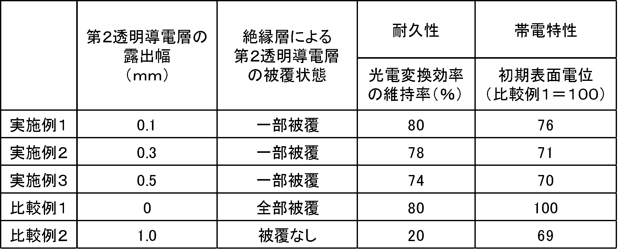
11a…透明基板の一面
12A,12B,12C,12D,12E…第1透明導電部(第1導電部)
12F…第2透明導電部(第2導電部)
12Fa…第2透明導電部の外周縁と第1の溝との間の幅が最大となる部分
33…絶縁層
33a…絶縁層の外周縁
50,50A~50D…光電変換セル
90A…第1の溝
90B…第2の溝
90E…第1の溝の端部
100,200,300…光電変換素子
112…透明導電層(導電層)
112X…第1透明導電層(第1導電層)
112Y…第2透明導電層(第2導電層)
112a…導電層の外周縁
W…第2透明導電部の外周縁と第1の溝との間の幅
W1…第2透明導電部の外周縁と絶縁層(又はその前駆体)の外周縁との間の幅
Wmax…Wの最大値
Claims (6)
- 第1基板と、
前記第1基板の一面上に設けられる導電層とを有し、
前記導電層が、少なくとも1つの第1導電部を有する第1導電層と、前記第1導電層の外側に設けられ、少なくとも1つの第2導電部を有する第2導電層とを有する光電変換素子であって、
少なくとも1つの光電変換セルを有し、
前記光電変換セルが、
前記第1導電部と、
前記第1導電部に対向する第2基板と、
前記第1基板及び前記第2基板を接合させる環状の封止部とを有し、
前記第1導電層と前記第2導電層とは第1の溝を介して配置され、
前記光電変換素子が絶縁層を有し、
前記絶縁層が、前記少なくとも1つの光電変換セルの前記封止部と前記第1基板との間で前記封止部と重なるように設けられ、
前記絶縁層の外周縁が、前記光電変換素子を前記第1基板の前記一面に直交する方向から見た場合に、前記封止部より外側に且つ前記少なくとも1つの光電変換セルにおける前記封止部全体を包囲するように設けられており、
前記絶縁層が、前記絶縁層の外周縁よりも内側で且つ前記封止部の外側で前記第1導電層のうち前記封止部の外側に出ている部分を覆い隠し、前記第1の溝に入り込むとともに前記第2導電層の一部を覆っており、
前記第2導電層の残部が露出されている、光電変換素子。 - 前記第1の溝の端部が前記導電層の外周縁に達しており、
前記絶縁層が前記第1の溝の端部にも入り込んでいる、請求項1に記載の光電変換素子。 - 前記少なくとも1つの光電変換セルが複数の前記光電変換セルで構成され、
前記第1導電層には、前記第1の溝とともに前記光電変換セルと同数の前記第1導電部を形成するように隣り合う前記第1導電部同士を離間させる第2の溝が形成され、前記第2の溝にも前記絶縁層が入り込んでいる、請求項1又は2に記載の光電変換素子。 - 前記絶縁層が前記第1の溝の全部に入り込んでいる、請求項1~3のいずれか一項に記載の光電変換素子。
- 前記第2導電部の外周縁と前記第1の溝との間の幅が最大となる部分における幅をWmaxとし、前記第2導電部が露出している幅をW1とした場合に、W1/Wmaxが0.1以上である、請求項1~4のいずれか一項に記載の光電変換素子。
- 前記絶縁層が、前記封止部の外側で前記第1導電層のうち前記封止部の外側に出ている部分の全部を覆い隠している、請求項1~5のいずれか一項に記載の光電変換素子。
Priority Applications (3)
| Application Number | Priority Date | Filing Date | Title |
|---|---|---|---|
| US15/775,117 US10395847B2 (en) | 2015-11-20 | 2016-11-18 | Photoelectric conversion element |
| CN201680050399.1A CN107924764B (zh) | 2015-11-20 | 2016-11-18 | 光电转换元件 |
| EP16866424.1A EP3376514A4 (en) | 2015-11-20 | 2016-11-18 | PHOTOELECTRIC CONVERSION ELEMENT |
Applications Claiming Priority (2)
| Application Number | Priority Date | Filing Date | Title |
|---|---|---|---|
| JP2015227550A JP6063026B1 (ja) | 2015-11-20 | 2015-11-20 | 光電変換素子 |
| JP2015-227550 | 2015-11-20 |
Publications (1)
| Publication Number | Publication Date |
|---|---|
| WO2017086424A1 true WO2017086424A1 (ja) | 2017-05-26 |
Family
ID=57800130
Family Applications (1)
| Application Number | Title | Priority Date | Filing Date |
|---|---|---|---|
| PCT/JP2016/084215 Ceased WO2017086424A1 (ja) | 2015-11-20 | 2016-11-18 | 光電変換素子 |
Country Status (5)
| Country | Link |
|---|---|
| US (1) | US10395847B2 (ja) |
| EP (1) | EP3376514A4 (ja) |
| JP (1) | JP6063026B1 (ja) |
| CN (1) | CN107924764B (ja) |
| WO (1) | WO2017086424A1 (ja) |
Cited By (1)
| Publication number | Priority date | Publication date | Assignee | Title |
|---|---|---|---|---|
| JP2019145663A (ja) * | 2018-02-20 | 2019-08-29 | 株式会社フジクラ | 光電変換素子 |
Families Citing this family (3)
| Publication number | Priority date | Publication date | Assignee | Title |
|---|---|---|---|---|
| US11569044B2 (en) | 2018-07-24 | 2023-01-31 | Sharp Kabushiki Kaisha | Solar battery unit and wireless transmitter including solar battery unit |
| JP7593319B2 (ja) * | 2019-08-02 | 2024-12-03 | 日本ゼオン株式会社 | 光電変換装置 |
| WO2023132136A1 (ja) | 2022-01-07 | 2023-07-13 | パナソニックホールディングス株式会社 | 光電変換モジュール |
Citations (3)
| Publication number | Priority date | Publication date | Assignee | Title |
|---|---|---|---|---|
| WO2011001815A1 (ja) * | 2009-06-29 | 2011-01-06 | シャープ株式会社 | 湿式太陽電池モジュール |
| JP5451920B1 (ja) * | 2013-03-30 | 2014-03-26 | 株式会社フジクラ | 色素増感太陽電池素子 |
| JP2014211951A (ja) | 2012-09-01 | 2014-11-13 | 株式会社フジクラ | 色素増感太陽電池素子 |
Family Cites Families (3)
| Publication number | Priority date | Publication date | Assignee | Title |
|---|---|---|---|---|
| US9947483B2 (en) * | 2012-09-01 | 2018-04-17 | Fujikura Ltd. | Dye-sensitized solar cell element |
| US20150372248A1 (en) * | 2013-02-06 | 2015-12-24 | Fujikura Ltd. | Dye-sensitized solar cell element |
| WO2015098914A1 (ja) * | 2013-12-24 | 2015-07-02 | 株式会社フジクラ | 光電変換素子 |
-
2015
- 2015-11-20 JP JP2015227550A patent/JP6063026B1/ja not_active Expired - Fee Related
-
2016
- 2016-11-18 EP EP16866424.1A patent/EP3376514A4/en not_active Withdrawn
- 2016-11-18 WO PCT/JP2016/084215 patent/WO2017086424A1/ja not_active Ceased
- 2016-11-18 US US15/775,117 patent/US10395847B2/en not_active Expired - Fee Related
- 2016-11-18 CN CN201680050399.1A patent/CN107924764B/zh not_active Expired - Fee Related
Patent Citations (3)
| Publication number | Priority date | Publication date | Assignee | Title |
|---|---|---|---|---|
| WO2011001815A1 (ja) * | 2009-06-29 | 2011-01-06 | シャープ株式会社 | 湿式太陽電池モジュール |
| JP2014211951A (ja) | 2012-09-01 | 2014-11-13 | 株式会社フジクラ | 色素増感太陽電池素子 |
| JP5451920B1 (ja) * | 2013-03-30 | 2014-03-26 | 株式会社フジクラ | 色素増感太陽電池素子 |
Non-Patent Citations (1)
| Title |
|---|
| See also references of EP3376514A4 |
Cited By (1)
| Publication number | Priority date | Publication date | Assignee | Title |
|---|---|---|---|---|
| JP2019145663A (ja) * | 2018-02-20 | 2019-08-29 | 株式会社フジクラ | 光電変換素子 |
Also Published As
| Publication number | Publication date |
|---|---|
| CN107924764B (zh) | 2019-12-03 |
| JP2017098358A (ja) | 2017-06-01 |
| US10395847B2 (en) | 2019-08-27 |
| EP3376514A4 (en) | 2019-08-14 |
| JP6063026B1 (ja) | 2017-01-18 |
| EP3376514A1 (en) | 2018-09-19 |
| US20180330892A1 (en) | 2018-11-15 |
| CN107924764A (zh) | 2018-04-17 |
Similar Documents
| Publication | Publication Date | Title |
|---|---|---|
| US10096431B2 (en) | Dye-sensitized solar cell element for low illuminance | |
| JP6063026B1 (ja) | 光電変換素子 | |
| JP6122156B2 (ja) | 光電変換素子 | |
| JP5802817B1 (ja) | 色素増感型光電変換素子 | |
| JP5451920B1 (ja) | 色素増感太陽電池素子 | |
| WO2015098914A1 (ja) | 光電変換素子 | |
| WO2014162639A1 (ja) | 色素増感太陽電池素子 | |
| JP6333343B2 (ja) | 光電変換素子 | |
| JP6143911B2 (ja) | 低照度用色素増感太陽電池素子 | |
| JP6573497B2 (ja) | 光電変換素子 | |
| JP5444488B1 (ja) | 色素増感太陽電池素子 | |
| JP6076573B1 (ja) | 光電変換素子 | |
| JP5380619B1 (ja) | 色素増感太陽電池素子 | |
| JP6694371B2 (ja) | 光電変換素子 | |
| JP6697348B2 (ja) | 光電変換素子 | |
| JP6598757B2 (ja) | 光電変換素子 | |
| JP2018081988A (ja) | 光電変換素子 | |
| JP6539146B2 (ja) | 光電変換素子 | |
| JP2019195019A (ja) | 光電変換素子 | |
| JP2017028095A (ja) | 光電変換素子 | |
| JP2018006489A (ja) | 光電変換素子 | |
| JP2016207949A (ja) | 光電変換素子 | |
| JP2016181568A (ja) | 光電変換素子 |
Legal Events
| Date | Code | Title | Description |
|---|---|---|---|
| 121 | Ep: the epo has been informed by wipo that ep was designated in this application |
Ref document number: 16866424 Country of ref document: EP Kind code of ref document: A1 |
|
| WWE | Wipo information: entry into national phase |
Ref document number: 15775117 Country of ref document: US |
|
| NENP | Non-entry into the national phase |
Ref country code: DE |
|
| WWE | Wipo information: entry into national phase |
Ref document number: 2016866424 Country of ref document: EP |
|
| ENP | Entry into the national phase |
Ref document number: 2016866424 Country of ref document: EP Effective date: 20180614 |