WO2020021982A1 - 太陽電池ユニットおよび太陽電池ユニットを備えた無線発信機 - Google Patents
太陽電池ユニットおよび太陽電池ユニットを備えた無線発信機 Download PDFInfo
- Publication number
- WO2020021982A1 WO2020021982A1 PCT/JP2019/026140 JP2019026140W WO2020021982A1 WO 2020021982 A1 WO2020021982 A1 WO 2020021982A1 JP 2019026140 W JP2019026140 W JP 2019026140W WO 2020021982 A1 WO2020021982 A1 WO 2020021982A1
- Authority
- WO
- WIPO (PCT)
- Prior art keywords
- substrate
- solar cell
- housing
- wireless transmitter
- antenna
- Prior art date
- Legal status (The legal status is an assumption and is not a legal conclusion. Google has not performed a legal analysis and makes no representation as to the accuracy of the status listed.)
- Ceased
Links
Images










Classifications
-
- H—ELECTRICITY
- H01—ELECTRIC ELEMENTS
- H01G—CAPACITORS; CAPACITORS, RECTIFIERS, DETECTORS, SWITCHING DEVICES, LIGHT-SENSITIVE OR TEMPERATURE-SENSITIVE DEVICES OF THE ELECTROLYTIC TYPE
- H01G9/00—Electrolytic capacitors, rectifiers, detectors, switching devices, light-sensitive or temperature-sensitive devices; Processes of their manufacture
- H01G9/20—Light-sensitive devices
- H01G9/2068—Panels or arrays of photoelectrochemical cells, e.g. photovoltaic modules based on photoelectrochemical cells
- H01G9/2081—Serial interconnection of cells
-
- G—PHYSICS
- G06—COMPUTING OR CALCULATING; COUNTING
- G06K—GRAPHICAL DATA READING; PRESENTATION OF DATA; RECORD CARRIERS; HANDLING RECORD CARRIERS
- G06K19/00—Record carriers for use with machines and with at least a part designed to carry digital markings
- G06K19/06—Record carriers for use with machines and with at least a part designed to carry digital markings characterised by the kind of the digital marking, e.g. shape, nature, code
- G06K19/067—Record carriers with conductive marks, printed circuits or semiconductor circuit elements, e.g. credit or identity cards also with resonating or responding marks without active components
- G06K19/07—Record carriers with conductive marks, printed circuits or semiconductor circuit elements, e.g. credit or identity cards also with resonating or responding marks without active components with integrated circuit chips
- G06K19/077—Constructional details, e.g. mounting of circuits in the carrier
-
- H—ELECTRICITY
- H01—ELECTRIC ELEMENTS
- H01Q—ANTENNAS, i.e. RADIO AERIALS
- H01Q1/00—Details of, or arrangements associated with, antennas
- H01Q1/12—Supports; Mounting means
- H01Q1/22—Supports; Mounting means by structural association with other equipment or articles
-
- H—ELECTRICITY
- H01—ELECTRIC ELEMENTS
- H01Q—ANTENNAS, i.e. RADIO AERIALS
- H01Q1/00—Details of, or arrangements associated with, antennas
- H01Q1/40—Radiating elements coated with or embedded in protective material
-
- H—ELECTRICITY
- H01—ELECTRIC ELEMENTS
- H01Q—ANTENNAS, i.e. RADIO AERIALS
- H01Q1/00—Details of, or arrangements associated with, antennas
- H01Q1/52—Means for reducing coupling between antennas; Means for reducing coupling between an antenna and another structure
- H01Q1/521—Means for reducing coupling between antennas; Means for reducing coupling between an antenna and another structure reducing the coupling between adjacent antennas
- H01Q1/523—Means for reducing coupling between antennas; Means for reducing coupling between an antenna and another structure reducing the coupling between adjacent antennas between antennas of an array
-
- H—ELECTRICITY
- H02—GENERATION; CONVERSION OR DISTRIBUTION OF ELECTRIC POWER
- H02S—GENERATION OF ELECTRIC POWER BY CONVERSION OF INFRARED RADIATION, VISIBLE LIGHT OR ULTRAVIOLET LIGHT, e.g. USING PHOTOVOLTAIC [PV] MODULES
- H02S40/00—Components or accessories in combination with PV modules, not provided for in groups H02S10/00 - H02S30/00
- H02S40/30—Electrical components
- H02S40/34—Electrical components comprising specially adapted electrical connection means to be structurally associated with the PV module, e.g. junction boxes
-
- H—ELECTRICITY
- H05—ELECTRIC TECHNIQUES NOT OTHERWISE PROVIDED FOR
- H05B—ELECTRIC HEATING; ELECTRIC LIGHT SOURCES NOT OTHERWISE PROVIDED FOR; CIRCUIT ARRANGEMENTS FOR ELECTRIC LIGHT SOURCES, IN GENERAL
- H05B47/00—Circuit arrangements for operating light sources in general, i.e. where the type of light source is not relevant
- H05B47/10—Controlling the light source
- H05B47/175—Controlling the light source by remote control
- H05B47/19—Controlling the light source by remote control via wireless transmission
-
- H—ELECTRICITY
- H10—SEMICONDUCTOR DEVICES; ELECTRIC SOLID-STATE DEVICES NOT OTHERWISE PROVIDED FOR
- H10F—INORGANIC SEMICONDUCTOR DEVICES SENSITIVE TO INFRARED RADIATION, LIGHT, ELECTROMAGNETIC RADIATION OF SHORTER WAVELENGTH OR CORPUSCULAR RADIATION
- H10F19/00—Integrated devices, or assemblies of multiple devices, comprising at least one photovoltaic cell covered by group H10F10/00, e.g. photovoltaic modules
-
- Y—GENERAL TAGGING OF NEW TECHNOLOGICAL DEVELOPMENTS; GENERAL TAGGING OF CROSS-SECTIONAL TECHNOLOGIES SPANNING OVER SEVERAL SECTIONS OF THE IPC; TECHNICAL SUBJECTS COVERED BY FORMER USPC CROSS-REFERENCE ART COLLECTIONS [XRACs] AND DIGESTS
- Y02—TECHNOLOGIES OR APPLICATIONS FOR MITIGATION OR ADAPTATION AGAINST CLIMATE CHANGE
- Y02E—REDUCTION OF GREENHOUSE GAS [GHG] EMISSIONS, RELATED TO ENERGY GENERATION, TRANSMISSION OR DISTRIBUTION
- Y02E10/00—Energy generation through renewable energy sources
- Y02E10/50—Photovoltaic [PV] energy
- Y02E10/542—Dye sensitized solar cells
Definitions
- the present disclosure relates to a technology of a solar cell unit equipped with a solar cell.
- Patent Document 1 discloses a communication device.
- a solar cell having a light receiving surface for receiving irradiation light, a power storage device provided on the back surface of the light receiving surface, and a communication antenna, and the power storage device is opposed to the solar cell.
- a circuit board provided on the back side of the surface.
- An object of the present disclosure is to provide a solar cell unit that suppresses a radio wave emitted by a communication antenna from being attenuated by a solar cell.
- a substrate, a solar cell mounted on the surface of the substrate, and an antenna supplied with power from the solar cell and mounted on the back surface of the substrate, the antenna includes a solar cell in a front view. And a solar cell unit arranged so as not to overlap the cells of the present invention.
- a solar cell unit that can suppress a radio wave transmitted from a communication antenna from being attenuated by a solar cell.
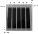
- FIG. 2 is a side cross-sectional view illustrating the entire configuration of the solar cell unit 100 according to the first embodiment. It is a photograph which shows the light-receiving surface side of the solar cell 110 of the solar cell unit 100 concerning 1st Embodiment.
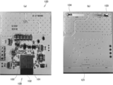
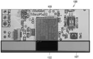
- 5A is a photograph showing the back surface of the substrate 120 according to the first embodiment
- FIG. 5B is a photograph showing the light receiving surface side of the substrate 120 of the solar cell unit 100 according to the first embodiment.
- FIG. 11 is a rear view showing a first glass substrate 111 and a second glass substrate 112 of a solar cell 110 according to a second embodiment. It is a side view showing the 1st glass substrate 111, the 2nd glass substrate 112, and substrate 120 of solar cell 110 concerning a 2nd embodiment.
- FIG. 11 is a rear view showing a first glass substrate 111 and a second glass substrate 112 of a solar cell 110 according to a second embodiment. It is a side view showing the 1st glass substrate 111, the 2nd glass substrate 112, and substrate 120 of solar cell 110 concerning a 2nd embodiment.
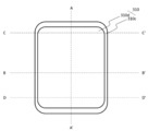
- FIG. 14 is a front view of a wireless transmitter 300 according to a fourth embodiment.
- FIG. 14 is a rear view of the wireless transmitter 300 according to the fourth embodiment.
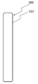
- FIG. 14 is a side view of a wireless transmitter 300 according to a fourth embodiment.
- FIG. 12 is a sectional view taken along line A-A ′ in FIG. 11.
- FIG. 12 is a sectional view taken along the line B-B ′ in FIG. 11.
- FIG. 12 is a sectional view taken along the line C-C ′ in FIG. 11.
- FIG. 12 is a sectional view taken along line D-D ′ in FIG. 11. It is B-B 'sectional drawing of the wireless transmitter 300 in 5th Embodiment.
- It is a front view of the radio transmitter 300 concerning a 6th embodiment.
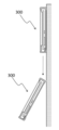
- radio transmitter 300 It is A-A 'sectional drawing of radio transmitter 300 in a 7th embodiment. It is an image figure showing a posture at the time of fall of radio transmitter 300 in a 7th embodiment. It is B-B 'sectional drawing of the wireless transmitter 300 in 9th Embodiment.
- solar cell unit 100 mainly includes solar cell 110, substrate 120, and communication module 130. Electronic components such as a capacitor for storing power generated by the solar cell 110 and a control IC may be further included.
- Solar cell 110 is mounted on the surface of substrate 120.
- the communication module 130 is mounted on the back surface of the board 120.
- the solar cell unit 100 performs various kinds of communication by the communication module 130 including the communication device 133 and the antenna 132 using the power generated by the solar cell 110.
- the communication module 130 including the communication device 133 and the antenna 132 using the power generated by the solar cell 110.
- the radio wave of the beacon can be periodically emitted while power is generated by light from indoor lights.
- a terminal such as a mobile phone that receives the radio wave of the beacon can accurately acquire its own position, or a server or the like can accurately acquire the position of the terminal.
- solar cell 110 includes first glass substrate 111 serving as a light receiving surface, and second glass substrate 112.
- a transparent conductive film is formed on the first glass substrate 111 on the second glass substrate 112 side.
- notches 112X and 112Y are formed at the end in the Y direction and the end in the X direction in FIG. 2 of the second glass substrate 112.
- the cutout portion 112Y of the transparent conductive film of the first glass substrate 111 becomes the negative output terminal 113 (first output terminal), and the cutout portion 112X becomes the positive output terminal 114 (second output terminal).
- the negative electrode output terminal 113 and the positive electrode output terminal 114 are formed on the back surface of the solar cell 110, that is, on the substrate 120 side.
- the material of the first glass substrate 111 is not particularly limited as long as it is a transparent substrate, and a film may be used instead of glass.
- the second glass substrate 112 can be replaced by a non-transparent substrate.
- the solar cell 110 is a monolithic dye-sensitized solar cell. As shown in FIG. 2, a plurality of vertically long cells 115, 115... Are arranged side by side in a lateral direction when viewed from the light receiving surface side of the solar cell 110. More specifically, solar cell 110 according to the present embodiment has a total output of 3 volts by connecting five cells 115 having an electromotive force of 0.6 volts in series.
- an area 210 for mounting the solar cell 110 is provided on the surface of the substrate 120, and a negative input terminal 123 is provided at a position facing the negative output terminal 113 of the solar cell 110.
- A first input terminal
- a positive input terminal 124 second input terminal
- a flat area 121 on which no electronic component or the like is mounted is formed on the opposite side away from the communication module 130.
- a portion on the back side of the area of the substrate 120 on the side of the negative pole input terminal 123 and the side of the positive pole input terminal 124, that is, the area away from the communication module 130 is formed flat.
- the flat area 121 includes an end portion of the substrate 120 and is preferably an integrated area of 1 / or more of the entire substrate 120.
- the distance from the end of the communication module 130 where the antenna 132 is arranged to the opposite end is Amm
- the distance from the opposite end to a position that is 1 / or more of Amm away from the opposite end It is preferable to keep it flat.
- the degree of flatness does not need to be flat to about 1 ⁇ m or about 1 nm, and if it is less than 1/10, more preferably less than 1/20 with respect to the size of the substrate 120, for example, Amm. Good.
- the substrate 120 can be stably held by placing the substrate 120 on the flat table 200 with the flat area 121 facing down, and Workability can be improved.
- the substrate 120 is placed on a flat table with the area being down. Accordingly, the substrate 120 can be stably held, and workability on the surface of the substrate 120 can be improved.
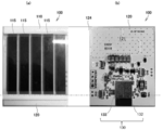
- the negative input terminal 123 and the positive input terminal 124 and the communication module 130 are arranged on the opposite sides of the substrate 120 with respect to the Y direction in FIG. As shown in FIGS. 5 to 8, the cells 115, 115... Of the solar cell 110 are closer to the minus pole input terminal 123 and the plus pole input terminal 124 with respect to the substrate 120. More specifically, the configuration is such that the cells 115 of the solar cell 110 do not extend to the antenna 132 of the communication module 130. In other words, the antenna 132 of the communication module 130 is configured such that the solar cell 110 is not stacked on the surface of the substrate 120 and is located on the non-conductive portion 127 of the substrate 120.
- the non-conductive portion 127 refers to a portion where the substrate 120 protrudes from the edge of the solar cell 110 by the shortest distance L as shown in FIG.
- a communication antenna 132 is provided on the back surface of the portion of the substrate 120 protruding from the edge of the solar cell 110. As shown in FIG. 8, it is preferable that no conductive material be disposed in the non-conductor portion 127 of the substrate 120 other than the communication antenna 132. This can reduce interference with the communication of the communication module 130 by the solar cell 110.
- the solar cell 110 and the communication module 130 are electrically connected to each other through a conductor (not shown) inside the substrate 120 provided from the negative pole input terminal 123 and the positive pole input terminal 124. That is, it is preferable that the conductive wires provided from the negative pole input terminal 123 and the positive pole input terminal 124 inside the substrate 120 are not exposed in the flat area 121 on the back surface of the substrate 120.
- the flat area 121 on the back surface of the substrate 120 may be formed of a resin covering the conductor.
- the communication module 130 has a rectangular shape, and the longitudinal direction of the antenna 132 of the communication module 130 is configured to be parallel to the edge of the substrate 120.
- the communication module 130 is mounted so that the antenna 132 does not protrude from the board 120 and fits inside the board 120. Therefore, it is possible to prevent the antenna 132 having low rigidity from being damaged.
- all or part of the antenna 132 may be configured so as to be parallel to the edge of the substrate 120 and along the edge of the substrate 120. That is, it is preferable that the long portion of the antenna 132 is arranged parallel to the edge of the substrate 120.
- the second glass substrate 112 may be cut not only at the notches 112X and 112Y but also at the entire end. That is, as shown in FIGS. 9 and 10, the first glass substrate 111 and the second glass substrate 112 are offset such that the edge of the second glass substrate 112 is inward of the edge of the first glass substrate 111. It may be stuck so that it does.
- the solar cell unit 100 after the first glass substrate 111 and the second glass substrate 112 are bonded together, the first glass substrate 111 and the first glass substrate Between the glass substrate 111 and the second glass substrate 112 is injected. Then, an ultraviolet curable resin 116 is applied to the back surface of the first glass substrate 111 and the side surface of the second glass substrate 112 so as to cover the inlet for the electrolyte. At this time, the ultraviolet curable resin 116 is not applied to the notches 112X and 112Y.
- the dye-sensitized solar cell 110 has been described, but another type of solar cell may be used.
- the communication module 130 is disposed at one end of the substrate 120 in the longitudinal direction of the cells 115 of the solar cell 110, and the cells 115, 115,.
- the negative input terminal 123 and the positive input terminal 124 are arranged at the other end in the longitudinal direction, but the communication module 130 is arranged at one short end of the cells 115 of the solar cell 110.
- the negative input terminal 123 and the positive input terminal 124 may be arranged at the other ends of the cells 115 of the battery 110 in the short direction.
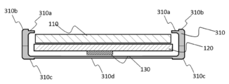
- FIG. 11 is a front view of a wireless transmitter 300 according to the fourth embodiment.
- FIG. 12 is a rear view of the wireless transmitter 300 according to the fourth embodiment.
- FIG. 13 is a side view of the wireless transmitter 300 according to the fourth embodiment.
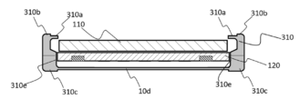
- FIG. 14 is a sectional view taken along the line A-A 'in FIG.
- FIG. 15 is a sectional view taken along the line B-B 'in FIG.
- FIG. 16 is a sectional view taken along the line C-C 'in FIG.
- FIG. 17 is a sectional view taken along the line D-D 'in FIG.
- the left side of the wireless transmitter 300 is referred to as the left side of the wireless transmitter 300
- the near side of the sheet of FIG. 11 is referred to as the front of the wireless transmitter 300
- the wireless transmitter 300 includes the solar cell unit 100 and a housing 310 that covers a part thereof.
- the solar cell 110 provided in the solar cell unit 100 is arranged so that external light can enter from outside the housing 310.
- the wireless transmitter 300 is provided with a fixture (not shown), and is used by being attached to a wall surface or a ceiling.
- case 310 is formed of an elastic member in order to reduce the impact that substrate 120 or solar cell 110 receives when falling from the wall surface on which wireless transmitter 100 is mounted.
- it is formed of a resin such as plastic or rubber.
- the radio transmitter 300 includes the housing 310, the substrate 120 on which the communication device 133 is mounted and the solar battery 110 held inside the housing 310, and the cells 115 and 115 of the solar battery 110. 115 are configured to easily receive external light without being covered by the housing 310.
- the housing 310 includes a front part 310a and a back part 310c.
- the front part 310a and the back part 310c are connected to each other by screws or the like.
- an opening 310x is formed in the front part 310a at a position where the solar cell 110 is located.
- the area of the opening 310x is smaller than the area of the substrate 120, but is preferably larger than the area of the solar cell 110.
- the area of the opening 310x may be smaller than the area of the solar cell 110 and larger than the area where the cells 115 are arranged.
- the substrate 120 and the substrate 120 side of the solar cell 110 are brought into contact with the back part 310c.
- the front part 310a and the back part 310c are closed in this state, the substrate 120 and the solar cell 110 are sandwiched between the front part 310a and the back part 310c.
- the left and right side surfaces of substrate 120 are sandwiched by left and right wall surfaces 310e, 310e inside housing 310.
- the substrate 120 when the substrate 120 is sandwiched between the housings 310 from the left and right directions, the substrate 120 is supported inside the housing 310 so as not to fall down. Note that in this state, it is preferable that other portions of the substrate 120, the solar cell 110, and the like do not contact the housing 310. Thus, even if the wireless transmitter 300 attached to a wall, a pillar, a ceiling, or the like falls, the possibility that the substrate 120 or the solar cell 110 hits the housing 300 and is damaged can be reduced.
- the left and right side surfaces of the substrate 120 are sandwiched by the left and right wall surfaces 310e, 310e inside the housing 300, the left and right side surfaces of the substrate 120 are applied by applying a force that does not damage the substrate 120. It is preferable to slide with respect to 310e. At this time, it is preferable that there is a space between the substrate 120 and the inner wall of the housing 310 in the vertical direction shown in FIG. 1 to allow the substrate 120 to slide.
- the left and right side surfaces of substrate 120 are sandwiched by left and right wall surfaces 310e, 310e inside case 310 so that the upper and lower side surfaces of substrate 120 are held at positions not in contact with case 310.
- a gap that is, a space is formed between a surface other than the left and right side surfaces of the substrate 120 and the inner wall surface of the housing 310.
- a configuration in which the upper and lower side surfaces of the substrate 120 are also sandwiched between inner wall surfaces of the housing 310 may be employed.
- one or more portions of the substrate 120 other than the above-described holding portion may directly or indirectly contact or be supported on the inner wall surface of the housing 310.
- the substrate 120 is held by the housing 310 with the front end of the solar cell 110 positioned behind the front end of the housing 310. That is, it is preferable that the solar cell 110 be held by the housing 310 in a state of being recessed inside the housing 310. This can reduce the possibility that the solar cell 110 contacts the floor surface even when the front surface side of the housing 310 contacts the floor surface or the like.
- the inside of the front part 310a of the housing 310 that is, the end 310b on the opening 310x side is recessed rearward.
- the edge of the housing 310 on the opening 310x side is formed in a convex shape toward the center of the opening 310x.
- the central part 310d in the front view or the rear view is formed to be thinner than the surrounding part in the front view or the rear view.
- the antenna 132 is located at a position close to the lower end (first end) of the substrate 120 in the vertical direction (second direction) intersecting at right angles to the horizontal direction (first direction) shown in FIG. It is preferred that When the length in the vertical direction (second direction) of the substrate 120 shown in FIG. 1 is W, the antenna 132 may be arranged in a range from the lower end (first end) of the substrate 120 to 1 / 3W or less. More preferably, it is more preferably arranged along the lower end (first end) of the substrate 120. Since the antenna 132 is located closer to the lower end (first end), the signal intensity of the signal transmitted by the antenna 132 is suppressed from being attenuated by the solar cell 110 attached to the surface of the substrate 120. .
- the position of the side surface of substrate 120 sandwiched between left and right side surfaces 310e, 310e of substrate 120 may be a position close to the upper end (second end) of substrate 120 as shown in FIG. preferable.
- the position of the side surface of the substrate 120 sandwiched between the left and right side surfaces of the substrate 120 is preferably located within a range of WW or less from the upper end (second end) of the substrate 120, and ⁇ ⁇ ⁇ W from the upper end. More preferably, it is located in the following range.
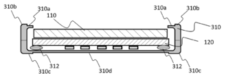
- an elastic member 312 softer than the material of the housing 310 may be provided between the substrate 120 and the housing 310 as shown in FIG. Thereby, when the wireless transmitter 300 falls, the impact which the board
- the elastic member 312 is not limited to the rear side of the substrate 120 and may be disposed between the lower surface, the upper surface, the side surface, or the like of the substrate 120 or the solar cell 110 and the inner wall surface of the housing 310.
- a wall-mounting member be attached to the upper end of the housing 310 as shown in FIG.
- the housing 310 can be easily attached to a wall or a pillar projection.
- case 310 preferably sandwiches substrate 120 and solar cell 110 such that antenna 132 side of substrate 120 is located below. That is, it is preferable that the wall surface attaching member 340 is attached to the end of the housing 310 that is farther from the antenna 132.
- a center-of-gravity adjusting unit 350 that is, a weight is attached to the back side inside the housing 310. More specifically, it is preferable that the weight of the center-of-gravity adjusting unit 350 is not less than 1/3 and not more than 3/2 of the total weight of the substrate 120 and the solar cell 110.
- the center-of-gravity adjustment unit 350 is not limited to the inside of the housing 310, and may be attached to the outside of the housing 310 near the rear surface.
- center-of-gravity adjusting unit 350 may be arranged on a part of the bottom surface of the housing 310, may be arranged widely on the entire bottom surface of the housing 310, or may be arranged around the bottom surface of the housing 310. May be done. ⁇ Eighth Embodiment>
- the case 310 is configured such that the front part 310a and the back part 310c can be bent together.
- the front part 310a and the back part 310c may be connected to each other such that the right part of the front part 310a and the left part of the back part 310c are rotatable, or the left part of the front part 310a may be connected to the front part 310a.
- the right part of the back part 310c may be rotatably connected, the upper part of the front part 310a and the upper part of the back part 310c may be rotatably connected, or the front part 310a And the lower part of the back part 310c may be rotatably connected.
- the front part 310a and the back part 310c may be bonded from the front.
- the front part 310a and the back part 310c may be detachably attached to each other, or may be fixed to each other with an adhesive or the like.
- the end 310 b of the housing 310 on the side of the opening 301 x may cover the edge of the solar cell 110. That is, the opening area of the opening 310x of the housing 310 is smaller than the substrate of the solar cell 110. With such a configuration, dust can be prevented from entering the housing 310 from the opening 310x.
Landscapes
- Engineering & Computer Science (AREA)
- Power Engineering (AREA)
- Microelectronics & Electronic Packaging (AREA)
- Chemical Kinetics & Catalysis (AREA)
- Electrochemistry (AREA)
- Chemical & Material Sciences (AREA)
- Computer Networks & Wireless Communication (AREA)
- Computer Hardware Design (AREA)
- Physics & Mathematics (AREA)
- General Physics & Mathematics (AREA)
- Theoretical Computer Science (AREA)
- Photovoltaic Devices (AREA)
- Details Of Aerials (AREA)
- Support Of Aerials (AREA)
Abstract
基板(120)と、基板(120)の裏面に取り付けられる太陽電池(110)と、基板(120)に取り付けられる通信モジュール(130)とを備える太陽電池ユニット(100)が提供される。通信モジュール(130)のアンテナ(132)は、表面視において、太陽電池(110)のセル(115,115・・・)と重ならないように配置される。
Description
本開示は、太陽電池を搭載した太陽電池ユニットの技術に関する。
従来から、太陽電池や通信アンテナを搭載した太陽電池ユニットが知られている。たとえば、国際公報第2017/013940号パンフレット(特許文献1)には、通信装置が開示されている。特許文献1によると、照射光を受光する受光面を有する太陽電池と、上記受光面の裏面上に設置される蓄電デバイスと、通信用アンテナを有し、上記蓄電デバイスの上記太陽電池との対向面の裏面上に設置される回路基板と、を備える、通信装置が提供される。
本開示の目的は、通信用のアンテナが発する電波が太陽電池によって減衰されることを抑制する太陽電池ユニットを提供することにある。
本開示の一態様に従うと、基板と、基板の表面に取り付けられる太陽電池と、前記太陽電池から電力が供給され、基板の裏面に取り付けられるアンテナとを備え、アンテナは、表面視において、太陽電池のセルと重ならないように配置される、太陽電池ユニットを提供される。
以上のように、本開示によれば、通信用のアンテナから発信される電波が太陽電池によって減衰することを抑制できる、太陽電池ユニットが提供される。
以下、図面を参照しつつ、本開示の実施の形態について説明する。以下の説明では、同一の部品には同一の符号を付してある。それらの名称および機能も同じである。したがって、それらについての詳細な説明は繰り返さない。
<第1の実施の形態>
<太陽電池ユニット100の全体構成>
<第1の実施の形態>
<太陽電池ユニット100の全体構成>
本実施の形態にかかる太陽電池ユニット100の全体構成について説明する。図1から図3を参照して、本実施の形態にかかる太陽電池ユニット100は、主に、太陽電池110と、基板120と、通信モジュール130とを含む。太陽電池110で発電した電力を溜めるコンデンサ、制御ICなどの電子部品をさらに含んでいてもよい。太陽電池110は、基板120の表面に取り付けられる。通信モジュール130は、基板120の裏面に取り付けられる。
本実施の形態にかかる太陽電池ユニット100は、太陽電池110で生み出した電力を利用して、通信デバイス133およびアンテナ132を含む通信モジュール130によって各種の通信を行うものである。たとえば、太陽電池110として色素増感太陽電池を利用し、通信モジュール130としてビーコンを利用することによって、屋内のライトからの光によって発電しながら、ビーコンの電波を定期的に発することができる。これによって、ビーコンの電波を受信する携帯電話などの端末が自身の位置を正確に取得したり、サーバなどで端末の位置を正確に取得したりすることができる。
より詳細には、太陽電池110は、受光面となる第1のガラス基板111と、第2のガラス基板112とを含む。第1のガラス基板111の、第2のガラス基板112側には、透明導電膜が形成されている。そして、第2のガラス基板112の、図2におけるY方向の端部かつX方向の端部、に切り欠き部112X,112Yが形成される。そして、第1のガラス基板111の透明導電膜の切り欠き部112Yがマイナス極出力端子113(第1の出力端子)となり、切り欠き部分112Xがプラス極出力端子114(第2の出力端子)となる。つまり、太陽電池110の裏面、すなわち基板120側に、マイナス極出力端子113とプラス極出力端子114とが形成される。
なお、第1のガラス基板111は透明な基板であれば特に材料は限定されず、ガラスの代わりにフィルムであってもよい。第2のガラス基板112は、透明ではない基板で代用できる。
なお、本実施の形態においては、太陽電池110は、モノリシック型の色素増感太陽電池である。図2に示すように、太陽電池110の受光面側の表面視において、複数の縦長のセル115,115・・・が短手方向に並べて配置されるものである。より詳細には、本実施の形態にかかる太陽電池110は、0.6ボルトの起電力を有するセル115を、5個直列につないで、全体的に3ボルトの出力を有する。
図3(b)に示すように、基板120の表面には、太陽電池110を載置するためのエリア210があり、太陽電池110のマイナス極出力端子113に対向する位置にマイナス極入力端子123(第1の入力端子)が取り付けられ、太陽電池110のプラス極出力端子114に対向する位置にプラス極入力端子124(第2の入力端子)が取り付けられる。
そして特に、本実施の形態においては、図3(a)に示すように、基板120の裏側においては、通信モジュール130と離れた反対側に電子部品などが実装されていないフラットなエリア121が形成されている。本実施の形態においては、基板120のうちの、マイナス極入力端子123側およびプラス極入力端子124側のエリアの裏側部分、すなわち通信モジュール130から離れたエリアがフラットに形成されている。
なお、フラットなエリア121は、基板120の端部を含み、基板120全体の1/3以上のまとまったエリアであることが好ましい。換言すれば、通信モジュール130のアンテナ132が配置されている端部から、それとは逆の端部までの距離をAmmとすると、当該逆の端部からAmmの1/3以上離れた位置までをフラットにしておくことが好ましい。
なお、フラットの程度は、1μmや1nm程度までフラットにする必要はなく、基板120の大きさ、たとえばAmmに対して、1/10未満の凹凸、より好ましくは1/20未満の凹凸であればよい。これによって、図4に示すように、当該フラットなエリア121を下にして基板120をフラットな台200に載置することによって、基板120を安定して保持することができ、基板120の表面に対する作業性を向上させることができる。
より詳細には、対象となるエリアに大きな凹凸があったとしても、凸部同士の表面の高さが同程度であればよく、当該エリアを下にして基板120をフラットな台に載置することによって、基板120を安定して保持することができ、基板120の表面に対する作業性を向上させることができる。
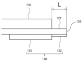
さらに、本実施の形態においては、マイナス極入力端子123およびプラス極入力端子124と、通信モジュール130と、が図2におけるY方向に関して、互いに基板120の逆側に配置される。そして、図5~図8に示すように、太陽電池110のセル115,115・・・が、基板120に対して、マイナス極入力端子123やプラス極入力端子124の方に寄っている。より詳細には、太陽電池110のセル115,115・・・が、通信モジュール130のアンテナ132まで延設されないように構成されている。換言すれば、通信モジュール130のアンテナ132が、基板120の表面において太陽電池110が積層されておらず、基板120の非導体部分127に位置するように構成されている。非導体部分127とは、図6が示すように、太陽電池110の縁から基板120が最短距離で距離Lだけ突出した部分を指す。基板120の太陽電池110の縁から突出した部分の裏面に通信用のアンテナ132が配されている。なお、図8が示すように、基板120の非導体部127において、通信用のアンテナ132以外に導電性材料が配されないことが好ましい。これによって、太陽電池110による、通信モジュール130の通信に対する妨害を低減することができる。
また、太陽電池110と通信モジュール130はマイナス極入力端子123およびプラス極入力端子124から配された基板120内部の導線(不図示)を通して電気的に接続される。つまり、マイナス極入力端子123およびプラス極入力端子124から配され基板120内部の導線は、基板120の裏面におけるフラットなエリア121において露出しないことが好ましい。基板120の裏面にフラットなエリア121は導線を覆う樹脂で形成されていてもよい。
また本実施の形態においては、通信モジュール130は方形形状であり、通信モジュール130のアンテナ132の長手方向が、基板120の縁と平行に構成されている。換言すれば、通信モジュール130は、アンテナ132が基板120からはみ出ることなく基板120内に収まるように実装されている。このため剛性が弱いアンテナ132の破損を防止することができる。
ただし、アンテナ132の全部または一部が、基板120の縁に平行に、基板120の縁に沿うように構成されてもよい。つまりアンテナ132の長尺部分が、基板120の縁に平行に配置されることが好ましい。
<第2の実施の形態>
<第2の実施の形態>
上記の実施の形態に加えて、第2のガラス基板112は、切り欠き部112X,112Yだけでなく、端部全体が切りかかれていてもよい。すなわち、図9および図10に示すように、第1のガラス基板111と第2のガラス基板112とが、第2のガラス基板112の縁が第1のガラス基板111の縁よりも内側にオフセットするように張り付けられてもよい。
より詳細には、本実施の形態にかかる太陽電池ユニット100に関しては、第1のガラス基板111と第2のガラス基板112とを貼り合わせた後に、上記のように両者のズレた部分から第1のガラス基板111と第2のガラス基板112との間に電解液を注入する。そして、電解液の注入口をふさぐように、第1のガラス基板111の裏面と第2のガラス基板112の側面に紫外線硬化性樹脂116を塗布する。このとき、切り欠き部112X,112Yには、紫外線硬化性樹脂116を塗布しない。
そして、紫外線硬化性樹脂116が固まると、紫外線硬化性樹脂116が第2のガラス基板112の表面よりも基板120側に飛び出さないように、紫外線硬化性樹脂116の表面を斜めに削り落とす。これによって、太陽電池110の端部と基板120の端部との間に隙間が生じ、入力端子123、124が第2のガラス基板112の切り欠き部112X、112Yにはめ込むことが容易になるため、太陽電池ユニット100を組み立てる際、作業性が向上する。
<第3の実施の形態>
<第3の実施の形態>
上記の実施の形態においては、色素増感太陽電池110に関して説明を行ったが、他の種類の太陽電池であってもよい。また、上記の実施の形態においては、基板120のうちの、太陽電池110のセル115,115・・・の長手方向の一端に通信モジュール130を配置し、太陽電池110のセル115,115・・・の長手方向の他端にマイナス極入力端子123およびプラス極入力端子124を配置したが、太陽電池110のセル115,115・・・の短手方向の一端に通信モジュール130を配置し、太陽電池110のセル115,115・・・の短手方向の他端にマイナス極入力端子123およびプラス極入力端子124を配置してもよい。
<第4の実施の形態>
<第4の実施の形態>
第4の実施の形態にかかる太陽電池ユニット100を備えた無線発信機300の全体構成について説明する。図11は、第4の実施の形態にかかる無線発信機300の正面図である。図12は、第4の実施の形態にかかる無線発信機300の背面図である。図13は、第4の実施の形態にかかる無線発信機300の側面図である。図14は、図11におけるA-A’断面図である。図15は、図11におけるB-B’断面図である。図16は、図11におけるC-C’断面図である。図17は、図11におけるD-D’断面図である。なお、以下では、図11における上方を無線発信機300の上方といい、図11における下方を無線発信機300の下方といい、図11における右方を無線発信機300の右方といい、図11における左方を無線発信機300の左方といい、図11における紙面の手前側を無線発信機300の前方といい、図11における紙面の奥側を無線発信機300の後方という。
本実施の形態にかかる無線発信機300は、太陽電池ユニット100と、その一部を覆う筐体310とを含む。太陽電池ユニット100に備えられた太陽電池110は、筐体310の外から外光が入射できるように配置される。また、無線発信機300は、図示しない取り付け具を備え、壁面や天井などに取り付けて使用する。
本実施の形態においては、筐体310は、無線発信機100が取り付けられていた壁面から落下した際に、基板120や太陽電池110が受ける衝撃を低減するために、弾性部材によって形成されている。たとえば、プラスチックやゴムなどの樹脂によって形成される。
特に本実施の形態にかかる無線発信機300は、筐体310によって、筐体310の内側に、通信デバイス133が実装された基板120や太陽電池110が保持されつつ、太陽電池110のセル115,115・・・は筐体310で覆われずに外部の光を受光しやすく構成されている。
より詳細には、筐体310は、正面側のパーツ310aと、裏面側のパーツ310cとを含む。正面側のパーツ310aと、裏面側のパーツ310cとは、ねじ等で互いに連結されている。
そして、正面側のパーツ310aには、太陽電池110が位置する部分に開口部310xが形成される。正面視において、開口部310xの面積は、基板120の面積よりも小さいが、太陽電池110の面積よりも大きいことが好ましい。ただし、開口部310xの面積は、太陽電池110の面積よりも小さくて、セル115,115・・・が配置されるエリアよりも大きい構成であってもよい。
本実施の形態においては、正面側のパーツ310aと裏面側のパーツ310cとを開いた状態で、基板120と太陽電池110の基板120側を裏面側のパーツ310cに接触させる。この状態で、正面側のパーツ310aと裏面側のパーツ310cとを閉じると、基板120と太陽電池110が、正面側のパーツ310aと裏面側のパーツ310cとに挟み込まれる。本実施の形態においては、この状態において、基板120の左右側面が、筐体310の内側の左右壁面310e,310eによって挟持される。
つまり、基板120が、左右方向から筐体310に挟まれることによって、基板120は筐体310の内側で下方へ落ち込まないように支持される。なお、この状態において、基板120の他の部分や、太陽電池110などが、筐体310に接触しないことが好ましい。これによって、仮に、壁や柱や天井などに取り付けられた無線発信機300が落下しても、基板120や太陽電池110が筐体300にぶつかって損傷する可能性を低減することができる。
基板120の左右側面が筐体300の内側の左右壁面310e,310eによって挟持された状態であっても、基板120が損傷しない程度の力を与えることによって、基板120の左右側面が左右壁面310e,310eに対してスライドすることが好ましい。このとき、図1に示す上下方向において、基板120と筐体310の内壁との間に、基板120がスライドすることを許容するための空間があることが好ましい。
なお、本実施の形態においては、基板120の上下側面が筐体310には接触しない位置に保持されるように、基板120の左右側面を筐体310の内側の左右壁面310e,310eによって挟持される。すなわち、基板120の左右側面以外の表面と筐体310の内壁面と間には隙間すなわち空間が形成されるものである。しかしながら、基板120の上下側面もが筐体310の内側の内壁面に挟持される構成であってもよい。あるいは、基板120のうちの、上記の挟持箇所以外の1または複数の箇所が、直接的に、または間接的に、筐体310の内壁面に接触したり支持されたりしてもよい。
また、太陽電池110の前端部が、筐体310の前端部よりも後方に位置した状態で、基板120が筐体310に保持される。つまり、太陽電池110が、筐体310の内側に凹んだ状態で、筐体310に保持されることが好ましい。これによって、筐体310の表面側が床面などに接触しても、太陽電池110が床面に接触する可能性を低減することができる。
さらに本実施の形態においては、筐体310の表側のパーツ310aは、内側部が、すなわち開口部310x側の端部310bが、後方へ窪んでいる。換言すれば、筐体310の開口部310x側の縁部が、開口部310xの中心に向かって凸形状に構成されている。これによって、太陽電池110が外部の物体に接触する可能性を低減することができる。
そして、筐体310の裏側のパーツ310cに関しては、正面視または背面視における中央部分310dが、正面視または背面視における周囲の部分よりも薄い形状に形成されている。
さらに本実施の形態においては、アンテナ132は、図1に示す左右方向(第1方向)と直角に交差する上下方向(第2方向)において、基板120の下端(第1端)に近い位置配置されていることが好ましい。図1に示す基板120の上下方向(第2方向)の長さをWとした場合、アンテナ132は基板120の下端(第1端)から1/3W以下までの範囲に配置されていることが好ましく、基板120の下端(第1端)に沿って配置されていることがより好ましい。アンテナ132がより下端(第1端)に近い位置に配置されていることで、アンテナ132が発信する信号の信号強度が基板120の表面に取り付けられた太陽電池110によって減衰されることを抑制する。
さらに本実施の形態においては、基板120の左右側面310e、310eによって挟持される基板120の側面の位置は、図11に示すように基板120の上端(第2端)に近い位置であることが好ましい。基板120の左右側面、によって挟持される基板120の側面の位置は、基板120の上端(第2端)から1/2W以下までの範囲に位置されていることが好ましく、さらに上端から1/3W以下までの範囲に位置されていることがより好ましい。
<第5の実施の形態>
<第5の実施の形態>
上記の実施の形態の構成に加えて、図18に示すように、基板120と、筐体310との間に筐体310の素材よりも柔らかい弾性部材312を配置してもよい。これによって、無線発信機300が落下した際に、基板120や太陽電池110が受ける衝撃をより低減することができる。なお、弾性部材312は、基板120の背面側に限らず、基板120や太陽電池110の下面や上面や側面などと筐体310の内壁面との間に配置されてもよい。
<第6の実施の形態>
<第6の実施の形態>
上記の実施の形態の構成に加えて、図19に示すように、筐体310の上端には、壁面取り付け部材が取り付けられることが好ましい。これによって、筐体310は、壁や柱の突起に容易に取り付けることができる。
より好ましくは、筐体310は、基板120のうちのアンテナ132側が下方に位置するように、基板120や太陽電池110を挟持することが好ましい。つまり、筐体310のうちの、アンテナ132とは遠い方の端部に壁面取り付け部材340が取り付けられることが好ましい。
<第7の実施の形態>
<第7の実施の形態>
上記の実施の形態の構成に加えて、図20に示すように、筐体310の内側には、その背面側に、重心調整部350、すなわち重りが取り付けられる。より詳細には、重心調整部350の重さは、基板120と太陽電池110の合計の重さの、1/3以上3/2以下であることが好ましい。
これによって、図21に示すように、無線発信機300が落下した際に、筐体310の背面が下側になる態勢となりやすく、太陽電池110の表面が床面に接触する可能性を低減することができる。
なお、重心調整部350は、筐体310の内側に限らず、筐体310の外側の背面付近に取り付けられてもよい。
また、重心調整部350は、筐体310の底面の一部に配置されてもよいし、筐体310の底面全体に幅広く配置されてもよいし、筐体310の底面の周囲に渡って配置されてもよい。
<第8の実施の形態>
<第8の実施の形態>
上記の実施の形態においては、筐体310が表側のパーツ310aと裏側のパーツ310cとが互いに折り曲げ可能に構成されるものであった。なお、表側のパーツ310aと裏側のパーツ310cとは、表側のパーツ310aの右部と裏側のパーツ310cの左部とが回動可能に連結されてもよいし、表側のパーツ310aの左部と裏側のパーツ310cの右部とが回動可能に連結されてもよいし、表側のパーツ310aの上部と裏側のパーツ310cの上部とが回動可能に連結されてもよいし、表側のパーツ310aの下部と裏側のパーツ310cの下部とが回動可能に連結されてもよい。
あるいは、表側のパーツ310aと裏側のパーツ310cとが正面から張り合わされてもよい。なお、表側のパーツ310aと裏側のパーツ310cとは着脱自在に張り合わされてもよいし、接着剤などによって互いに固着されるものであってもよい。
<第9の実施の形態>
<第9の実施の形態>
上記の実施の形態の構成に加えて、図22に示すように、筐体310の開口部301xの側の端部310bが太陽電池110の縁を覆っていてもよい。つまり、筐体310の開口部310xの開口面積は、太陽電池110の基板よりも小さい。このような構成を有することで、開口部310xから筐体310内へ粉塵が混入することを防ぐことができる。
〔援用の記載〕
〔援用の記載〕
本願は、2018年7月24日に出願された特願2018-138848、2018年7月24日に出願された特願2018-138849および2018年7月24日に出願された特願2018-138850号に基づく優先権を主張するものであり、これらの出願の開示内容の全てを本願に援用する。
Claims (14)
- 第1の基板と、
前記第1の基板の主面に取り付けられる太陽電池と、
前記太陽電池から電力が供給され、前記第1の基板の前記主面に対する裏面に取り付けられるアンテナとを備え、
前記アンテナは、前記表面視において、前記太陽電池のセルと重ならないように配置される、太陽電池ユニット。 - 前記アンテナは、その長手方向が前記第1の基板の縁と平行になるように配置される、請求項1に記載の太陽電池ユニット。
- 前記基板の主面には、前記アンテナとは逆の端部に前記太陽電池と電気的に接続した第1の入力端子および第2の入力端子が設けられる、請求項1または2に記載の太陽電池ユニット。
- さらに、前記第1の基板の主面に設けられ、前記太陽電池と電気的に接続した第1の入力端子および第2の入力端子とを備え、
前記第1の基板の裏面のうち、少なくとも前記第1の入力端子および第2の入力端子の反対側に位置する部分にフラットな面が形成されている、請求項1または2に記載の太陽電池ユニット。 - 前記太陽電池は、
前記第1の入力端子と対向する第1の出力端子と、
前記第2の入力端子と対向する第2の出力端子とを備え、
前記第1の出力端子と前記第2の出力端子が同じ面に設けられる、請求項3または4に記載の太陽電池ユニット。 - 前記太陽電池は、
受光面となる第1の透明基板と、
前記第1の透明基板と対向し、前記第1の基板の表面に積層される第2の基板と、
前記第1の透明基板の前記第2の基板側に配された透明導電膜とを備え、
前記第1の出力端子および前記第2の出力端子は、前記透明導電膜が露出した部分で形成されていることを特徴とする請求項5に記載の太陽電池ユニット。 - 前記請求項1から6のいずれかに記載の太陽電池ユニットを備えた、無線発信機。
- 前記請求項1から6のいずれかに記載の太陽電池ユニットを収容する筺体と、
前記筐体は、前記第1の基板の側面の一部を挟持し、
前記筐体が前記第1の基板の側面の一部を挟持している方向を水平方向とし、前記水平方向と直角に交差する方向を鉛直方向において、前記アンテナは、前記筐体が前記第1基板の側面を挟持している位置よりも低い位置にあり、
前記第1の基板の側面と、前記筐体の内壁と、の間に空間を有する、請求項7に記載の無線発信機。 - 前記請求項1から6のいずれかに記載の太陽電池ユニットを収容する筺体と、
前記筐体は、前記第1の基板の側面の一部を挟持し、
前記筐体が前記第1の基板の側面の一部を挟持している方向を第1方向とし、前記第1方向と直角に交差する方向を第2方向において、
前記アンテナは、前記第1の基板の第1端側に設けられ、
前記筐体が前記第1の基板の側面を挟持している位置は、前記アンテナよりも前記基板の第1端と反対に位置する第2端側に位置し、
前記第1の基板の側面と、前記筐体の内壁と、の間に空間を有する、請求項7に記載の無線発信機。 - 前記第1の基板は略方形であって、
前記第2方向における基板の長さをWとした場合、
前記アンテナは、第1端から1/3Wまでの範囲に配置されている、無線発信機。 - 前記第1の基板は略方形であって、
前記第2方向における基板の長さをWとした場合、
前記第1の基板が挟持される位置は、前記第2端から1/2Wまでの範囲に配置されている、請求項9または10に記載の無線発信機。 - 前記筐体に挟持されている前記第1の基板の側面は摺動可能である、請求項8から11のいずれか1項に記載の無線発信機。
- 前記筺体は、前記太陽電池の受光面を露出する開口部を有し、
前記開口部の開口面積は、前記太陽電池の前記受光面の受光面積よりも大きく、前記第1の基板の面積よりも小さい、請求項7から請求項12のいずれか1項に記載の無線発信機。 - 前記開口部の開口面積は、前記太陽電池の受光面の受光面積よりも大きく、前記第2の基板よりも小さい、請求項8から13のいずれか1項に記載の無線発信機。
Priority Applications (2)
| Application Number | Priority Date | Filing Date | Title |
|---|---|---|---|
| JP2020532247A JP6975859B2 (ja) | 2018-07-24 | 2019-07-01 | 太陽電池ユニットおよび太陽電池ユニットを備えた無線発信機 |
| US17/260,457 US11569044B2 (en) | 2018-07-24 | 2019-07-01 | Solar battery unit and wireless transmitter including solar battery unit |
Applications Claiming Priority (6)
| Application Number | Priority Date | Filing Date | Title |
|---|---|---|---|
| JP2018138848 | 2018-07-24 | ||
| JP2018138849 | 2018-07-24 | ||
| JP2018-138850 | 2018-07-24 | ||
| JP2018-138849 | 2018-07-24 | ||
| JP2018138850 | 2018-07-24 | ||
| JP2018-138848 | 2018-07-24 |
Publications (1)
| Publication Number | Publication Date |
|---|---|
| WO2020021982A1 true WO2020021982A1 (ja) | 2020-01-30 |
Family
ID=69181554
Family Applications (1)
| Application Number | Title | Priority Date | Filing Date |
|---|---|---|---|
| PCT/JP2019/026140 Ceased WO2020021982A1 (ja) | 2018-07-24 | 2019-07-01 | 太陽電池ユニットおよび太陽電池ユニットを備えた無線発信機 |
Country Status (3)
| Country | Link |
|---|---|
| US (1) | US11569044B2 (ja) |
| JP (1) | JP6975859B2 (ja) |
| WO (1) | WO2020021982A1 (ja) |
Citations (5)
| Publication number | Priority date | Publication date | Assignee | Title |
|---|---|---|---|---|
| JP2006145558A (ja) * | 2003-05-09 | 2006-06-08 | Seiko Epson Corp | 無線通信機能付電子時計 |
| JP2011163913A (ja) * | 2010-02-09 | 2011-08-25 | Citizen Holdings Co Ltd | 電波時計 |
| JP2016167604A (ja) * | 2012-09-01 | 2016-09-15 | 株式会社フジクラ | 低照度用色素増感太陽電池素子 |
| JP2017037057A (ja) * | 2015-08-06 | 2017-02-16 | セイコーエプソン株式会社 | 電子時計 |
| JP2017098358A (ja) * | 2015-11-20 | 2017-06-01 | 株式会社フジクラ | 光電変換素子 |
Family Cites Families (7)
| Publication number | Priority date | Publication date | Assignee | Title |
|---|---|---|---|---|
| CN100487606C (zh) | 2003-05-09 | 2009-05-13 | 精工爱普生株式会社 | 具有无线通信功能的电子钟表 |
| US20080013409A1 (en) * | 2006-07-11 | 2008-01-17 | Bland Diarmuid John St Cullom | Timepiece with overlapping, separately driven analog and mechanical functionality |
| WO2010113708A1 (ja) * | 2009-03-30 | 2010-10-07 | 三菱マテリアル株式会社 | 太陽電池モジュールの製造方法 |
| US9147794B2 (en) * | 2011-11-30 | 2015-09-29 | First Solar, Inc. | Three terminal thin film photovoltaic module and their methods of manufacture |
| WO2014034913A1 (ja) | 2012-09-01 | 2014-03-06 | 株式会社フジクラ | 低照度用色素増感太陽電池素子 |
| JP2014160957A (ja) | 2013-02-20 | 2014-09-04 | Murata Mfg Co Ltd | アンテナ装置 |
| JP6907940B2 (ja) | 2015-07-21 | 2021-07-21 | ソニーグループ株式会社 | 通信装置 |
-
2019
- 2019-07-01 US US17/260,457 patent/US11569044B2/en active Active
- 2019-07-01 JP JP2020532247A patent/JP6975859B2/ja not_active Expired - Fee Related
- 2019-07-01 WO PCT/JP2019/026140 patent/WO2020021982A1/ja not_active Ceased
Patent Citations (5)
| Publication number | Priority date | Publication date | Assignee | Title |
|---|---|---|---|---|
| JP2006145558A (ja) * | 2003-05-09 | 2006-06-08 | Seiko Epson Corp | 無線通信機能付電子時計 |
| JP2011163913A (ja) * | 2010-02-09 | 2011-08-25 | Citizen Holdings Co Ltd | 電波時計 |
| JP2016167604A (ja) * | 2012-09-01 | 2016-09-15 | 株式会社フジクラ | 低照度用色素増感太陽電池素子 |
| JP2017037057A (ja) * | 2015-08-06 | 2017-02-16 | セイコーエプソン株式会社 | 電子時計 |
| JP2017098358A (ja) * | 2015-11-20 | 2017-06-01 | 株式会社フジクラ | 光電変換素子 |
Also Published As
| Publication number | Publication date |
|---|---|
| JP6975859B2 (ja) | 2021-12-01 |
| US20210304971A1 (en) | 2021-09-30 |
| JPWO2020021982A1 (ja) | 2021-08-19 |
| US11569044B2 (en) | 2023-01-31 |
Similar Documents
| Publication | Publication Date | Title |
|---|---|---|
| JP6995862B2 (ja) | カメラモジュールおよびモバイル端末 | |
| EP3832993B1 (en) | Handheld electronic device | |
| EP3832797B1 (en) | Handheld electronic device | |
| US20210168231A1 (en) | Handheld electronic device | |
| US10516814B2 (en) | Camera assembly and electronic device | |
| US7957123B2 (en) | Portable electronic device | |
| US7744296B2 (en) | Camera module having colloid layer surrounding sensor | |
| US20140255016A1 (en) | Device for driving camera lens module in portable terminal | |
| CN207968641U (zh) | 摄像头模块 | |
| CN101285919A (zh) | 相机模组 | |
| US11463039B2 (en) | Energy harvester | |
| WO2019052332A1 (zh) | 显示屏组件及移动终端 | |
| TWI672552B (zh) | 鏡頭模組 | |
| JP2010041709A (ja) | カメラモジュール | |
| JP2007128995A (ja) | 撮像素子のfpcに対する取り付け構造 | |
| JP2015144412A (ja) | 電子機器 | |
| CN108924402B (zh) | 摄像模组及终端设备 | |
| CN113489890B (zh) | 拍摄装置以及电子设备 | |
| US8901784B2 (en) | Voice coil motor with spacer | |
| JP6975859B2 (ja) | 太陽電池ユニットおよび太陽電池ユニットを備えた無線発信機 | |
| CN115811718A (zh) | 一种控制器 | |
| JP6764937B2 (ja) | 部品の取付構造および端末 | |
| JP4657610B2 (ja) | 携帯端末装置 | |
| JP4260646B2 (ja) | 携帯端末装置 | |
| CN121152148A (zh) | 电子设备、壳体组件和中框 |
Legal Events
| Date | Code | Title | Description |
|---|---|---|---|
| 121 | Ep: the epo has been informed by wipo that ep was designated in this application |
Ref document number: 19842083 Country of ref document: EP Kind code of ref document: A1 |
|
| ENP | Entry into the national phase |
Ref document number: 2020532247 Country of ref document: JP Kind code of ref document: A |
|
| NENP | Non-entry into the national phase |
Ref country code: DE |
|
| 122 | Ep: pct application non-entry in european phase |
Ref document number: 19842083 Country of ref document: EP Kind code of ref document: A1 |