WO2017104635A1 - 光学装置 - Google Patents
光学装置 Download PDFInfo
- Publication number
- WO2017104635A1 WO2017104635A1 PCT/JP2016/086992 JP2016086992W WO2017104635A1 WO 2017104635 A1 WO2017104635 A1 WO 2017104635A1 JP 2016086992 W JP2016086992 W JP 2016086992W WO 2017104635 A1 WO2017104635 A1 WO 2017104635A1
- Authority
- WO
- WIPO (PCT)
- Prior art keywords
- light
- light emitting
- optical device
- emitting side
- light receiving
- Prior art date
- Legal status (The legal status is an assumption and is not a legal conclusion. Google has not performed a legal analysis and makes no representation as to the accuracy of the status listed.)
- Ceased
Links
Images


Classifications
-
- H—ELECTRICITY
- H10—SEMICONDUCTOR DEVICES; ELECTRIC SOLID-STATE DEVICES NOT OTHERWISE PROVIDED FOR
- H10F—INORGANIC SEMICONDUCTOR DEVICES SENSITIVE TO INFRARED RADIATION, LIGHT, ELECTROMAGNETIC RADIATION OF SHORTER WAVELENGTH OR CORPUSCULAR RADIATION
- H10F55/00—Radiation-sensitive semiconductor devices covered by groups H10F10/00, H10F19/00 or H10F30/00 being structurally associated with electric light sources and electrically or optically coupled thereto
- H10F55/20—Radiation-sensitive semiconductor devices covered by groups H10F10/00, H10F19/00 or H10F30/00 being structurally associated with electric light sources and electrically or optically coupled thereto wherein the electric light source controls the radiation-sensitive semiconductor devices, e.g. optocouplers
- H10F55/25—Radiation-sensitive semiconductor devices covered by groups H10F10/00, H10F19/00 or H10F30/00 being structurally associated with electric light sources and electrically or optically coupled thereto wherein the electric light source controls the radiation-sensitive semiconductor devices, e.g. optocouplers wherein the radiation-sensitive devices and the electric light source are all semiconductor devices
- H10F55/255—Radiation-sensitive semiconductor devices covered by groups H10F10/00, H10F19/00 or H10F30/00 being structurally associated with electric light sources and electrically or optically coupled thereto wherein the electric light source controls the radiation-sensitive semiconductor devices, e.g. optocouplers wherein the radiation-sensitive devices and the electric light source are all semiconductor devices formed in, or on, a common substrate
-
- G—PHYSICS
- G01—MEASURING; TESTING
- G01J—MEASUREMENT OF INTENSITY, VELOCITY, SPECTRAL CONTENT, POLARISATION, PHASE OR PULSE CHARACTERISTICS OF INFRARED, VISIBLE OR ULTRAVIOLET LIGHT; COLORIMETRY; RADIATION PYROMETRY
- G01J1/00—Photometry, e.g. photographic exposure meter
- G01J1/02—Details
- G01J1/04—Optical or mechanical part supplementary adjustable parts
- G01J1/0407—Optical elements not provided otherwise, e.g. manifolds, windows, holograms, gratings
- G01J1/0437—Optical elements not provided otherwise, e.g. manifolds, windows, holograms, gratings using masks, aperture plates, spatial light modulators, spatial filters, e.g. reflective filters
-
- G—PHYSICS
- G01—MEASURING; TESTING
- G01V—GEOPHYSICS; GRAVITATIONAL MEASUREMENTS; DETECTING MASSES OR OBJECTS; TAGS
- G01V8/00—Prospecting or detecting by optical means
- G01V8/10—Detecting, e.g. by using light barriers
- G01V8/12—Detecting, e.g. by using light barriers using one transmitter and one receiver
-
- H—ELECTRICITY
- H10—SEMICONDUCTOR DEVICES; ELECTRIC SOLID-STATE DEVICES NOT OTHERWISE PROVIDED FOR
- H10F—INORGANIC SEMICONDUCTOR DEVICES SENSITIVE TO INFRARED RADIATION, LIGHT, ELECTROMAGNETIC RADIATION OF SHORTER WAVELENGTH OR CORPUSCULAR RADIATION
- H10F77/00—Constructional details of devices covered by this subclass
- H10F77/40—Optical elements or arrangements
- H10F77/413—Optical elements or arrangements directly associated or integrated with the devices, e.g. back reflectors
-
- H—ELECTRICITY
- H10—SEMICONDUCTOR DEVICES; ELECTRIC SOLID-STATE DEVICES NOT OTHERWISE PROVIDED FOR
- H10F—INORGANIC SEMICONDUCTOR DEVICES SENSITIVE TO INFRARED RADIATION, LIGHT, ELECTROMAGNETIC RADIATION OF SHORTER WAVELENGTH OR CORPUSCULAR RADIATION
- H10F77/00—Constructional details of devices covered by this subclass
- H10F77/50—Encapsulations or containers
-
- H—ELECTRICITY
- H10—SEMICONDUCTOR DEVICES; ELECTRIC SOLID-STATE DEVICES NOT OTHERWISE PROVIDED FOR
- H10H—INORGANIC LIGHT-EMITTING SEMICONDUCTOR DEVICES HAVING POTENTIAL BARRIERS
- H10H20/00—Individual inorganic light-emitting semiconductor devices having potential barriers, e.g. light-emitting diodes [LED]
- H10H20/80—Constructional details
- H10H20/85—Packages
- H10H20/855—Optical field-shaping means, e.g. lenses
Definitions
- the present invention relates to an optical device, and more particularly to an optical device having light emitting and light receiving functions.
- Patent Document 1 discloses a photo interrupter as an example of a conventional optical device.
- the photo interrupter includes a light emitting element and a light receiving element mounted on a substrate. The light emitted from the light emitting element is reflected by the detection target and then received by the light receiving element. Thereby, it can be detected that the detection target exists at a position facing the photo interrupter.
- Such a photo interrupter is used in a predetermined electronic device, for example.
- this opening is desirably small from the viewpoint of protecting components provided in the electronic apparatus.
- the conventional photo interrupter has room for improvement in terms of reducing the aperture.
- the present invention has been conceived under the circumstances described above, and an object of the present invention is to provide an optical device capable of downsizing a light passage opening provided in an electronic device or the like. .
- An optical device provided by one aspect of the present invention includes a light emitting unit that emits light forward in a first direction, and a light receiving unit that is disposed rearward in the first direction with respect to the light emitting unit.
- the light emitting unit has a light emitting side through hole that allows light traveling backward in the first direction to pass therethrough, and the light receiving unit has a light receiving unit that receives the light that has passed through the light emitting side through hole. ing.
- the light emitting unit has a light emitting side main surface facing the front in the first direction, a light emitting side rear surface facing the rear in the first direction, and a light emitting side base material having a light emitting side recess recessed from the light emitting side main surface;
- the light emitting side wiring formed in the light emitting side base material and the light emitting element accommodated in the light emitting side concave portion are provided, and the light emitting side through hole is connected to the light emitting side main surface and the light emitting side rear surface. It is configured.
- the light emitting side main surface and the light emitting side rear surface are perpendicular to the first direction.
- the light emitting side concave portion includes a light emitting side concave bottom surface facing forward in the first direction, and a light emitting side concave side surface connecting the light emitting side main surface and the light emitting side concave bottom surface.
- the light emitting side recess side surface is parallel to the first direction.
- the light emitting side concave side surface is inclined with respect to the first direction.
- the light emitting side wiring has a light emitting side bottom surface part formed on the light emitting side concave bottom surface.
- the light emitting element is bonded to the light emitting side bottom surface portion.
- the light emitting side wiring has a light emitting side surface portion formed on a side surface of the light emitting side concave portion.
- the light emitting side wiring has a light emitting side through portion extending from the light emitting side recess to the light emitting side wiring.
- the light emitting side wiring has a light emitting side rear surface portion formed on the light emitting side rear surface and conducting to the light emitting side through portion.
- the inner surface of the light emitting side through hole is parallel to the first direction.
- the inner surface of the light emitting side through hole is inclined with respect to the first direction.
- the light emitting unit includes a light emitting side translucent resin that fills the light emitting side concave portion, covers the light emitting element, and transmits light from the light emitting element.
- the light emitting side translucent resin has a light emitting side lens part.
- the light emitting side translucent resin has a light emitting side inclined surface inclined with respect to the light emitting side main surface.
- the light receiving unit has a light receiving side main surface facing the front in the first direction, a light receiving side rear surface facing the rear in the first direction, and a light receiving side base having a light receiving side recess recessed from the light receiving side main surface, A light-receiving-side wiring formed on the light-receiving-side base material; and a light-receiving element housed in the light-receiving-side recess and having the light-receiving portion.
- the light-receiving side main surface and the light-receiving side back surface are perpendicular to the first direction.
- the light receiving side concave portion includes a light receiving side concave bottom surface facing forward in the first direction, and a light receiving side concave side surface connecting the light receiving side main surface and the light receiving side concave bottom surface.
- the side surface of the light receiving side recess is parallel to the first direction.
- the light receiving side wiring has a light receiving side bottom surface portion formed on the bottom surface of the light receiving side concave portion.
- the light receiving unit includes a light receiving side wire that connects the light receiving element and the light receiving side bottom surface portion.
- the light receiving side wiring has a light receiving side through portion extending from the light receiving side recess to the light receiving side rear surface.
- the light receiving side wiring has a light receiving side back surface portion formed on the light receiving side back surface and conducting to the light receiving side through portion.
- the light receiving unit includes a light receiving side translucent resin that fills the light receiving side recess and covers the light receiving element and transmits light received by the light receiving unit.
- the light receiving side translucent resin has a light receiving side lens portion.
- the light receiving side translucent resin has a light receiving side inclined surface inclined with respect to the light receiving side main surface.
- the light-receiving side translucent resin has a through-hole portion that passes through the light-emitting side through-hole and is exposed to the light-emitting side main surface side.
- the light-receiving side translucent resin has a light-receiving side lens part formed at the front end in the first direction of the through-hole part.
- the light-receiving side translucent resin has a light-receiving side inclined surface formed at the front end in the first direction of the through-hole portion.
- it further includes a bonding material for bonding the light emitting side back surface of the light emitting side base material and the light receiving side back surface of the light receiving side base material.
- the bonding material is an anisotropic conductive bonding material.
- the bonding material is solder.
- a light-transmitting cover is further provided in front of the light-emitting side base material in the first direction, covers the light-emitting side recess and the light-emitting side through hole, and transmits light from the light-emitting element.
- the translucent cover has a light emitting side lens portion through which light from the light emitting element passes.
- the translucent cover has a light receiving side lens portion through which light traveling toward the light emitting side through hole passes.
- the light receiving unit includes a light receiving element having the light receiving unit.
- the optical device of the present invention when the light emitted from the light emitting portion of the light emitting unit is reflected by the detection object, the reflected light reaches the light receiving portion through the light emitting side through hole.
- the light emitting portion and the light receiving portion are provided at different positions in a predetermined direction (first direction). For this reason, it is possible to avoid the light emitting portion and the light receiving portion from interfering with each other, and the distance between the light emitting portion and the light receiving portion in the x direction (a direction perpendicular to the first direction) is reduced. It is possible. Therefore, in an electronic device or the like in which the optical device is mounted, an opening for allowing light to pass can be reduced in size.
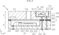
- FIG. 3 is a sectional view taken along line III-III in FIG. 1.
- the illustrated optical device A1 includes a light emitting unit 1, a light receiving unit 2, and a bonding material 3.
- the optical device A1 is a photo interrupter, and after the light emitted from the light emitting unit 1 is reflected by the detection target, the reflected light is received by the light receiving unit 2, thereby detecting the presence or absence of the detection target.
- the optical device A1 has a rectangular shape as viewed in the z direction, but the present invention is not limited to this.
- FIG. 1 is a plan view showing the optical device A1.
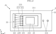
- FIG. 2 is a plan view of a main part of the optical device A1 in which the light emitting unit 1 and the light receiving unit 2 are omitted.
- FIG. 3 is a sectional view taken along line III-III in FIG.
- the light emitting unit 1 is responsible for the light emitting function of the optical device A1.
- the light emitting unit 1 includes a light emitting side substrate 11, a light emitting side wiring 12, a light emitting element 13, and a light emitting side translucent resin 14.
- the light emitting side base material 11 is a base of the light emitting unit 1, and at least the surface layer is made of an insulating material.
- Specific examples of the light emitting side substrate 11 include a semiconductor substrate made of a semiconductor material such as Si, a ceramic substrate made of alumina, etc., and a resin substrate made of glass epoxy resin, etc., but the present invention is not limited to this. is not.
- the resin substrate includes, for example, an MID substrate.
- the light emitting side substrate 11 has a light emitting side main surface 111, a light emitting side back surface 112, a light emitting side recess 113, and a light emitting side through hole 116.
- the light emitting side main surface 111 faces forward in the z direction and is perpendicular to the z direction.
- the light emitting side rear surface 112 faces rearward in the z direction and is perpendicular to the z direction.
- the light emitting side recess 113 is recessed from the light emitting side main surface 111.
- the illustrated light emitting side recess 113 is rectangular when viewed in the z direction, but the present invention is not limited to this.
- the light emission side recess 113 has a light emission side recess bottom surface 114 and a light emission side recess side surface 115.
- the light emitting side concave bottom surface 114 faces the front in the z direction and is parallel to the light emitting side main surface 111.
- the light emitting side concave side surface 115 connects the light emitting side concave bottom surface 114 and the light emitting side main surface 111.
- the light emitting side concave side surface 115 is parallel to the z direction.
- the light emitting side wiring 12 is formed on the light emitting side substrate 11 and constitutes a conduction path for supplying power to the light emitting element 13.
- the light emitting side wiring 12 is made of, for example, a single kind or a plurality of kinds of metals appropriately selected from Cu, Ni, Ti, Au, etc., and is formed by plating, for example.
- the light emitting side wiring 12 has a light emitting side bottom surface portion 121, a light emitting side side surface portion 122, a light emitting side through portion 123, and a light emitting side back surface portion 124.
- the light emitting side bottom surface portion 121 covers the light emitting side concave bottom surface 114. As shown in FIG. 2 and FIG. 3, the light emitting side bottom surface portion 121 includes two regions that are separated from each other in the x direction and are partitioned by slits that extend in the y direction.
- the light emitting side surface portion 122 covers the light emitting side recess side surface 115. Similarly to the light emission side bottom surface portion 121, the light emission side surface portion 122 includes two regions that are separated from each other in the x direction and are partitioned by slits extending in the z direction.
- the light emitting side through-hole 123 penetrates the light emitting side base material 11 from the light emitting side concave bottom surface 114 to the light emitting side rear surface 112.
- two light-emitting side through portions 123 are provided.
- the two light emitting side through-holes 123 are connected to the two regions of the light emitting side bottom surface portion 121 separately.
- the light emitting side back surface portion 124 is provided on the light emitting side back surface 112.
- two light emitting side rear surface portions 124 are provided.
- the two light emitting side rear surface portions 124 are connected to the two light emitting side through portions 123 separately.
- the light emitting element 13 is a light source of the light emitting unit 1. Specific examples of the light emitting element 13 include an LED element, an LD element, and a VCSEL element.
- the illustrated light emitting element 13 is, for example, an LED element that emits infrared light.
- the light emitting element 13 has a light emitting element electrode 131.
- the light emitting element 13 has a back surface electrode (not shown).
- the back electrode is bonded to one region of the light emitting side bottom surface portion 121 by a conductive bonding material.
- the light emitting element electrode 131 and the other region of the light emitting side bottom surface portion 121 are connected by a light emitting side wire 139.
- the light emitting side wire 139 is made of, for example, Au.
- the light-emitting side translucent resin 14 is filled in the light-emitting side recess 113 and covers the light-emitting element 13.
- the light emitting side translucent resin 14 is made of a material that transmits light from the light emitting element 13.
- the surface facing the front in the z direction of the light-emitting side translucent resin 14 is a flat surface or a surface gently recessed rearward in the z direction.
- the light receiving unit 2 is responsible for the light receiving function of the optical device A1.
- the light receiving unit 2 includes a light receiving side base material 21, a light receiving side wiring 22, and a light receiving element 23.
- the light-receiving side base material 21 serves as a foundation of the light-receiving unit 2, and at least the surface layer is made of an insulating material.
- Specific examples of the light receiving side base material 21 include a semiconductor substrate made of a semiconductor material such as Si, a ceramic substrate made of alumina, etc., and a resin substrate made of glass epoxy resin, etc., but the present invention is not limited to this. is not.
- the resin substrate includes, for example, an MID substrate.
- the light receiving side substrate 21 has a light receiving side main surface 211, a light receiving side back surface 212, and a light receiving side recess 213.
- the light-receiving side main surface 211 faces forward in the z direction and is perpendicular to the z direction.
- the light receiving side rear surface 212 faces rearward in the z direction and is perpendicular to the z direction.
- the light receiving side recess 213 is recessed from the light receiving side main surface 211.
- the light-receiving side recess 213 has a rectangular shape as viewed in the z direction, but the present invention is not limited to this.
- the light receiving side concave portion 213 has a light receiving side concave bottom surface 214 and a light receiving side concave side surface 215.
- the light receiving side concave bottom surface 214 faces the front in the z direction and is parallel to the light receiving side main surface 211.
- the light receiving side concave side surface 215 connects the light receiving side concave bottom surface 214 and the light receiving side main surface 211.
- the light receiving side concave side surface 215 is parallel to the z direction.
- the light receiving side wiring 22 is formed on the light receiving side base material 21 and constitutes a conduction path that conducts to the light receiving element 23.
- the light receiving side wiring 22 is made of, for example, a single kind or a plurality of kinds of metals appropriately selected from Cu, Ni, Ti, Au, etc., and is formed by plating, for example.
- the light receiving side wiring 22 of the present embodiment has a light receiving side bottom surface part 221, a light receiving side through part 222, a light receiving side back surface part 223, and a light receiving side main surface part 224.
- the light receiving side bottom surface portion 221 is formed on the light receiving side concave bottom surface 214. As shown in FIGS. 1 and 2, in the illustrated example, a plurality of light receiving side bottom surface portions 221 are provided. The plurality of light receiving side bottom surface portions 221 are arranged in the y direction on one side in the x direction of the light receiving side concave bottom surface 214, for example.
- the light-receiving side main surface portion 224 is provided on the light-receiving side base material 21.
- two light receiving side main surface portions 224 are provided.
- the two light receiving side main surface portions 224 are arranged at positions overlapping the two light emitting side rear surface portions 124 of the light emitting unit 1 when viewed in the z direction.
- the light-receiving side penetrating part 222 penetrates the light-receiving side base material 21 from the light-receiving side back surface 212 upward (in the direction of the light-receiving side main surface 211).
- a plurality of light-receiving side through portions 222 are provided.
- the two light receiving side through portions 222 that are relatively long are connected to the two light receiving side main surface portions 224 separately.
- the other relatively short light receiving side through-holes 222 are connected to the plurality of light receiving side bottom surface portions 221 separately.
- the light receiving side back surface part 223 is provided on the light receiving side back surface 212.
- a plurality of light receiving side rear surface portions 223 are provided.
- the two light receiving side rear surface portions 223 are connected to the two light receiving side through portions 222 separately.
- the other light receiving side back surface part 223 is connected to each of the plurality of light receiving side through parts 222 connected to the plurality of light receiving side bottom surface parts 221.
- the plurality of light receiving side rear surface portions 223 are used as mounting terminals when the optical device A1 is mounted on a circuit board such as an electronic device.
- the light receiving element 23 has a light receiving function of the light receiving unit 2. Specific examples of the light receiving element 23 include a phototransistor, a photodiode, and a photo IC. The illustrated light receiving element 23 is, for example, a photo IC. The light receiving element 23 is bonded to the light receiving side concave bottom surface 214 with a bonding material (not shown). The light receiving element 23 includes a plurality of light receiving element electrodes 231 and a light receiving unit 232.
- the light receiving part 232 is a part that receives light.
- the light receiving element 23 has a photoelectric conversion function for generating an electromotive force according to the light received by the light receiving unit 232.
- the plurality of light receiving element electrodes 231 and the plurality of light receiving side bottom surface portions 221 are connected to each other by a plurality of light receiving side wires 239.
- the light receiving side wire 239 is made of, for example, Au.
- the bonding material 3 bonds the light emitting unit 1 and the light receiving unit 2 together.
- the light emitting side back surface 112 of the light emitting unit 1 and the light receiving side main surface 211 of the light receiving unit 2 are joined.
- the bonding material 3 is an anisotropic conductive bonding material.
- the light-emitting side through hole 116 of the light-emitting unit 1 overlaps the light-receiving portion 232 of the light-receiving unit 2 in the z-direction view.
- the light emitting side through hole 116 entirely overlaps the light receiving unit 232 when viewed in the z direction.
- the light emitting side concave portion 113 and the light receiving side concave portion 213 are partially overlapped with each other when viewed in the z direction.
- a part of the light emitting element 13 overlaps a part of the light receiving side recess 213.
- a part of the light receiving element 23 overlaps a part of the light emitting side recess 113.
- the light L1 is emitted from the light emitting element 13 of the light emitting unit 1.
- the detection target exists in front of the z direction
- the light L1 is reflected by the detection target.
- the reflected light L ⁇ b> 2 passes through the light emitting side through hole 116 and is received by the light receiving unit 232.
- the light receiving element 23 outputs a detection signal corresponding to the received light by the photoelectric conversion function.
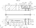
- FIG. 4 shows one process in an example of the manufacturing method of the optical device A1.
- the light emitting side rear surface 112 and the light receiving side main surface 211 are bonded together by the bonding material 3.
- a plurality of optical devices A1 may be manufactured by collectively cutting the light emitting side substrate and the light receiving side substrate.
- the reflected light L2 reaches the light receiving unit 232 through the light emitting side through hole 116.
- the light emitting part of the light emitting unit 1 and the light receiving part 232 of the light receiving unit 2 are provided at different positions in the z direction and are separated from each other. For this reason, it is possible to avoid interference between the light emitting portion of the light emitting unit 1 and the light receiving portion 232 in the x direction and the y direction, and the distance in the x direction between the light emitting portion and the light receiving portion 232 can be reduced. is there. Therefore, in an electronic device or the like in which the optical device A1 is mounted, the opening for allowing the light L1 and the light L2 to pass can be reduced in size.
- the light emitting unit 1 and the light receiving unit 2 may be formed separately and then joined. For this reason, it is not necessary to mount the light emitting element 13 and the light receiving element 23 close to each other. Therefore, the small optical device A1 can be easily manufactured.
- the light emitting unit 1 and the light receiving unit 2 can be manufactured more easily by adopting the light emitting unit 1 having the light emitting side substrate 11 and the light receiving unit 2 having the light receiving side substrate 21.
- the light emitted from the light emitting element 13 can be reflected by the light emitting side bottom surface portion 121 and the light emitting side surface portion 122. Thereby, the brightness of the light emitting unit 1 can be increased.
- the light emitting side back surface portion 124 that is electrically connected to the light emitting element 13 can be disposed on the light emitting side back surface 112 of the light emitting side substrate 11. This is advantageous for conducting the light receiving unit 2 and the light emitting element 13 while joining the light emitting unit 1 and the light receiving unit 2.
- the dimension of the optical device A1 in the x direction can be reduced.
- the configuration in which each of the light emitting element 13 and the light receiving side concave portion 213 overlaps each other in the z direction view or the configuration in which each of the light receiving element 23 and the light emitting side concave portion 113 overlap each other in the z direction view is a small size of the optical device A1. It is preferable for the modification.
- FIG. 5 shows a modification of the optical device based on the first embodiment.
- the bonding material 3 is made of solder.
- the two light emitting side rear surface portions 124 and the two light receiving side main surface portions 224 are bonded together by the bonding material 3 that is separated from each other.
- a part of the light emitting side wiring 12 that does not conduct to the light emitting element 13 is formed on the light emitting side rear surface 112 of the light emitting side base material 11, and the light emitting element 13 and the light receiving side main surface 211 of the light receiving side base material 21 are formed.
- a part of the light receiving side wiring 22 that is not electrically connected to the light receiving element 23 is formed. These portions are joined together by a joining material 3.
- the opening for allowing the light L1 and the light L2 to pass through can be reduced in an electronic device or the like on which the optical device A1 is mounted.
- the bonding material 3 can be appropriately applied regardless of whether it is an anisotropic conductive bonding material or solder.
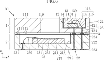
- FIG. 6 shows an optical device A1 according to another modification.
- the entire light receiving portion 232 of the light receiving element 23 of the light receiving unit 2 is enclosed in the light emitting side through hole 116 of the light emitting unit 1 as viewed in the z direction.
- the opening for allowing the light L1 and the light L2 to pass through can be reduced in an electronic device or the like on which the optical device A1 is mounted.
- the light emitting side through hole 116 and the light receiving portion 232 may be configured such that a part thereof overlaps each other when viewed in the z direction.
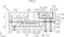
- FIG. 7 shows an optical device according to the second embodiment of the present invention.
- a light emitting side back surface concave portion 117 is formed in the light emitting side base material 11 of the light emitting unit 1.
- the light emitting side back surface recess 117 is recessed from the light emitting side back surface 112 and overlaps at least a part of the light receiving side wire 239 of the light receiving unit 2 when viewed in the z direction. Further, all of the light emitting side rear surface concave portion 117 is included in the light receiving side concave portion 213 of the light receiving side base material 21 as viewed in the z direction. Further, in the z direction, a part of the light receiving side wire 239 (z direction front side portion) is accommodated in the light emitting side back surface concave portion 117.
- the opening for allowing the light L1 and the light L2 to pass through can be reduced in the electronic apparatus or the like in which the optical device A2 is mounted. Further, by accommodating the light receiving side wire 239 by the light emitting side back surface concave portion 117, it is possible to avoid interference between the light receiving side wire 239 and the light emitting side base material 11. Further, by overlapping the light emitting side back surface concave portion 117 and the light receiving side wire 239 in the z direction, the dimension in the z direction of the optical device A2 can be reduced.
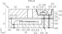
- FIG. 8 shows an optical device according to the third embodiment of the present invention.
- the light emitting side concave side surface 115 of the light emitting side base material 11 of the light emitting unit 1 is inclined with respect to the z direction.
- the light emitting side recess side surface 115 is inclined so that the cross-sectional shape along the xy plane of the light emitting side recess 113 becomes larger in the z direction from the light emitting side recess bottom surface 114 toward the light emitting side main surface 111. Yes.
- the opening for allowing the light L1 and the light L2 to pass through can be reduced in size in an electronic device or the like in which the optical device A3 is mounted.
- the light emitting side recess side surface 115 by inclining the light emitting side recess side surface 115, the light traveling in the lateral direction (x direction or y direction) from the light emitting element 13 is reflected by the light emitting side surface portion 122, and thus proceeds forward in the z direction. Can do. This is advantageous for increasing the luminance of the light emitting unit 1 and is preferable for improving the detection accuracy of the optical device A3.
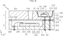
- FIG. 9 shows a modification of the optical device based on the third embodiment.
- the inner surface of the light emitting side through hole 116 is inclined with respect to the z direction. Specifically, the inner surface of the light emitting side through hole 116 is inclined such that the cross-sectional shape along the xy plane of the light emitting side through hole 116 increases in the z direction from the light emitting side rear surface 112 toward the light emitting side main surface 111. is doing.
- the opening for allowing the light L1 and the light L2 to pass through can be reduced in an electronic device or the like on which the optical device A3 is mounted.
- the opening for allowing the light L1 and the light L2 to pass through can be reduced in an electronic device or the like on which the optical device A3 is mounted.
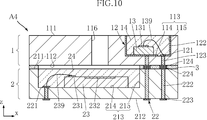
- FIG. 10 shows an optical device according to the fourth embodiment of the present invention.
- the light receiving unit 2 includes a light receiving side translucent resin 24.
- the light-receiving side translucent resin 24 is filled in the light-receiving side recess 213 and covers the light-receiving element 23.
- the light receiving element 23 is made of a material that transmits light received by the light receiving unit 232.
- the manufacture of the optical device A4 of this example for example, in the formation of the light receiving unit 2, if the light receiving side light transmitting resin 24 is formed by filling the light receiving side recess 213 with a light transmitting resin material and curing it. Good.
- the opening for allowing the light L1 and the light L2 to pass through can be reduced in the electronic apparatus or the like on which the optical device A4 is mounted. Further, the light receiving element 23 can be protected by the light receiving side translucent resin 24.
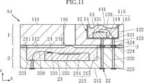
- FIG. 11 shows a modification of the optical device based on the fourth embodiment.
- a light receiving side lens portion 241 is formed in the light receiving side translucent resin 24.
- the light-receiving side lens unit 241 is located in front of the light-receiving unit 232 in the z direction, and overlaps the light-emitting side through hole 116 when viewed in the z direction.
- the light-receiving side lens portion 241 has a shape bulging forward in the z direction.
- the light emitting side lens portion 141 is formed on the light emitting side translucent resin 14.
- the light emitting side lens unit 141 is located in front of the light emitting element 13 in the z direction.
- the light emitting side lens portion 141 has a shape that bulges forward in the z direction.
- the opening for allowing the light L1 and the light L2 to pass through can be reduced in an electronic device or the like on which the optical device A4 is mounted.
- the detection effect of the optical device A4 can be further enhanced by the light condensing effect of the light emitting side lens unit 141 and the light receiving side lens unit 241.
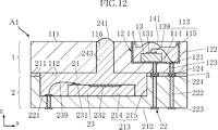
- FIG. 12 shows another modification of the optical device based on the fourth embodiment.
- the light-receiving side translucent resin 24 has a through-hole portion 243.
- the through hole portion 243 is a portion that passes through the light emitting side through hole 116 and is exposed to the light emitting side main surface 111 side.
- a light receiving side lens portion 241 is formed at the front end in the z direction of the through hole portion 243.
- the manufacture of the optical device A4 of this modification for example, after joining the light emitting unit 1 and the light receiving unit 2 in a state where the light receiving side translucent resin 24 is not formed, the light receiving side concave portion 213 and the light emitting side through hole 116 are joined.
- the light-receiving side translucent resin 24 may be formed by filling a translucent resin material and curing it.
- the opening for allowing the light L1 and the light L2 to pass through can be reduced in an electronic device or the like on which the optical device A4 is mounted.
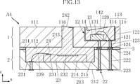
- FIG. 13 shows another modification of the optical device based on the fourth embodiment.
- the light emitting side light-transmitting resin 14 is formed with the light emitting side inclined surface 142
- the light receiving side light transmitting resin 24 is formed with the light receiving side inclined surface 242.
- the light emitting side inclined surface 142 is located in front of the light emitting element 13 in the z direction.
- the light emitting side inclined surface 142 is inclined with respect to the light emitting side main surface 111, and in the illustrated example, the light emitting side inclined surface 142 is inclined so as to be positioned forward in the z direction toward the right side in the x direction diagram.
- the light-receiving side inclined surface 242 is formed at the front end of the through-hole portion 243 in the z direction.
- the light receiving side inclined surface 242 is inclined with respect to the light emitting side main surface 111.
- the light receiving side inclined surface 242 is inclined so as to be positioned forward in the z direction toward the left in the x direction diagram.
- the opening for allowing the light L1 and the light L2 to pass through can be reduced in an electronic device or the like on which the optical device A4 is mounted. Further, the light from the light emitting element 13 is refracted by the light emitting side inclined surface 142. Thereby, the advancing direction of the light from the light emitting element 13 can be adjusted. Further, the light coming toward the light receiving unit 232 is refracted by the light receiving side inclined surface 242. Thereby, the direction in which the light received by the light receiving unit 232 comes can be adjusted. The direction and angle at which the light emitting side inclined surface 142 and the light receiving side inclined surface 242 are inclined may be appropriately changed according to the direction and angle of light to be adjusted.
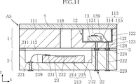
- FIG. 14 shows an optical device according to the fifth embodiment of the present invention.
- the illustrated optical device A ⁇ b> 5 includes a translucent cover 4.
- the translucent cover 4 is arranged forward in the first direction with respect to the light emitting side base material 11 and covers the light emitting side recess 113 and the light emitting side through-hole 116.
- the translucent cover 4 is made of a material that transmits light from the light emitting element 13. Examples of such a material include translucent resin and glass.
- the translucent cover 4 is joined to the light emission side main surface 111 of the light emission side base material 11.
- the opening for allowing the light L1 and the light L2 to pass through can be reduced in the electronic device or the like on which the optical device A5 is mounted. Further, the light-emitting element 13 and the light-receiving element 23 can be appropriately protected by the translucent cover 4.
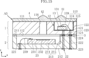
- FIG. 15 shows a modification of the optical device based on the fifth embodiment.
- the translucent cover 4 includes a light emitting side lens portion 41 and a light receiving side lens portion.
- the light emitting side lens portion 41 is disposed in front of the light emitting element 13 in the z direction.
- the light emitting side lens unit 41 bulges forward in the z direction.
- the light-receiving side lens portion 42 is disposed in front of the light-emitting side through hole 116 in the z direction.
- the light-receiving side lens portion 42 bulges forward in the z direction.
- the opening for allowing the light L1 and the light L2 to pass through can be reduced in an electronic device or the like on which the optical device A5 is mounted.
- the detection accuracy of the optical device A5 can be increased by the light condensing effect of the light emitting side lens unit 41 and the light receiving side lens unit.
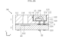
- FIG. 16 shows an optical device according to the sixth embodiment of the present invention.
- the illustrated optical apparatus A6 is different from the above-described embodiments in that the light receiving unit 2 is substantially constituted by only the light receiving element 23.
- the light receiving element 23 of the present embodiment is approximately the same size as the light emitting unit 1 (light emitting side base material 11) when viewed in the z direction.
- the light receiving element 23 has a light receiving portion 232.
- the light receiving unit 232 overlaps the light emitting side through hole 116 when viewed in the z direction.
- the light receiving element 23 is formed with a plurality of light receiving side rear surface portions 223. These light receiving side back surface portions 223 are used as mounting terminals.
- the light receiving element 23 is formed with a plurality of light receiving side main surface portions 224.
- the plurality of light receiving side main surface portions 224 are electrically connected to the plurality of light emitting side rear surface portions 124 of the light emitting unit 1 through the bonding material 3.
- the conduction between the light receiving side back surface part 223 and the light receiving side main surface part 224 is realized by a conduction path (not shown) formed in the light receiving element 23, a plating layer (not shown) formed on the side surface of the light receiving element 23, and the like. .
- the opening for allowing the light L1 and the light L2 to pass through can be reduced in size in an electronic device or the like in which the optical device A6 is mounted.
- the light receiving unit 2 of the present embodiment is configured by the light receiving element 23 and does not have the light receiving side base material 21 described above. Thereby, size reduction of optical apparatus A6 can be achieved.
- optical device according to the present invention is not limited to the above-described embodiment.
- the specific configuration of each part of the optical device according to the present invention can be modified in various ways.
Landscapes
- Physics & Mathematics (AREA)
- General Physics & Mathematics (AREA)
- Life Sciences & Earth Sciences (AREA)
- General Life Sciences & Earth Sciences (AREA)
- Geophysics (AREA)
- Spectroscopy & Molecular Physics (AREA)
- Photo Coupler, Interrupter, Optical-To-Optical Conversion Devices (AREA)
- Engineering & Computer Science (AREA)
- Microelectronics & Electronic Packaging (AREA)
Abstract
光学装置は、発光ユニットおよび受光ユニットを備える。前記発光ユニットは、第1方向前方に光を出射する。前記発光ユニットは、前記第1方向後方に進行する光を通過させる発光側貫通孔を有する。前記受光ユニットは、前記発光ユニットに対して前記第1方向後方に配置されている。前記受光ユニットは、前記発光側貫通孔を通過した光を受光する受光部を有している。
Description
本発明は、光学装置に関し、特に、発光および受光機能を有する光学装置に関する。
特許文献1には、従来の光学装置の一例としてフォトインタラプタが開示されている。当該フォトインタラプタは、基板に搭載された発光素子および受光素子を備える。発光素子が発した光は、検出対象物によって反射された後、受光素子によって受光される。これにより、当該フォトインタラプタに対向する位置に検出対象物が存在することを検出することができる。
このようなフォトインタラプタは、たとえば所定の電子機器に内蔵されて使用される。この場合、発光素子からの光および受光素子が受光する光を通過させるための共通の開口を当該電子機器のケースに設ける必要がある。この開口は、たとえば、電子機器内に設けられた部品の保護の観点からは、小さいことが望ましい。しかしながら、従来のフォトインタラプタは、開口を小さくするという点において、改善の余地があった。
本発明は、上記した事情のもとで考え出されたものであって、電子機器等に設けられる光通過用の開口を小型化することが可能な光学装置を提供することをその課題とする。
本発明の1つの側面により提供される光学装置は、第1方向前方に光を出射する発光ユニットと、前記発光ユニットに対して前記第1方向後方に配置された受光ユニットと、を備えており、前記発光ユニットは、前記第1方向後方に進行する光を通過させる発光側貫通孔を有しており、前記受光ユニットは、前記発光側貫通孔を通過した光を受光する受光部を有している。
好ましくは、前記発光ユニットは、前記第1方向前方を向く発光側主面、前記第1方向後方を向く発光側裏面、および前記発光側主面から凹む発光側凹部を有する発光側基材と、前記発光側基材に形成された発光側配線と、前記発光側凹部に収容された発光素子と、を具備しており、前記発光側貫通孔は、前記発光側主面および発光側裏面に繋がる構成とされている。
好ましくは、前記発光側主面および前記発光側裏面は、前記第1方向に対して直角である。
好ましくは、前記発光側凹部は、前記第1方向前方を向く発光側凹部底面と、前記発光側主面および前記発光側凹部底面を繋ぐ発光側凹部側面と、を有する。
好ましくは、前記発光側凹部側面は、前記第1方向に平行である。
好ましくは、前記発光側凹部側面は、前記第1方向に対して傾斜している。
好ましくは、前記発光側配線は、前記発光側凹部底面に形成された発光側底面部を有する。
好ましくは、前記発光素子は、前記発光側底面部に接合されている。
好ましくは、前記発光側配線は、前記発光側凹部側面に形成された発光側側面部を有する。
好ましくは、前記発光側配線は、前記発光側凹部から前記発光側配線に延びる発光側貫通部を有する。
好ましくは、前記発光側配線は、前記発光側裏面に形成され且つ前記発光側貫通部に導通する発光側裏面部を有する。
好ましくは、前記発光側貫通孔の内面は、前記第1方向に平行である。
好ましくは、前記発光側貫通孔の内面は、前記第1方向に対して傾斜している。
好ましくは、前記発光ユニットは、前記発光側凹部に充填されるとともに前記発光素子を覆い且つ前記発光素子からの光を透過する発光側透光樹脂を具備する。
好ましくは、前記発光側透光樹脂は、発光側レンズ部を有する。
好ましくは、前記発光側透光樹脂は、前記発光側主面に対して傾斜した発光側傾斜面を有する。
好ましくは、前記受光ユニットは、前記第1方向前方を向く受光側主面、前記第1方向後方を向く受光側裏面および前記受光側主面から凹む受光側凹部を有する受光側基材と、前記受光側基材に形成された受光側配線と、前記受光側凹部に収容され且つ前記受光部を有する受光素子と、を具備する。
好ましくは、前記受光側主面および前記受光側裏面は、前記第1方向に対して直角である。
好ましくは、前記受光側凹部は、前記第1方向前方を向く受光側凹部底面と、前記受光側主面および前記受光側凹部底面を繋ぐ受光側凹部側面と、を有する。
好ましくは、前記受光側凹部側面は、前記第1方向に平行である。
好ましくは、前記受光側配線は、前記受光側凹部底面に形成された受光側底面部を有する。
好ましくは、前記受光ユニットは、前記受光素子と前記受光側底面部とを接続する受光側ワイヤを具備する。
好ましくは、前記受光側配線は、前記受光側凹部から前記受光側裏面に延びる受光側貫通部を有する。
好ましくは、前記受光側配線は、前記受光側裏面に形成され且つ前記受光側貫通部に導通する受光側裏面部を有する。
好ましくは、前記受光ユニットは、前記受光側凹部に充填されるとともに前記受光素子を覆い且つ前記受光部が受光する光を透過する受光側透光樹脂を具備する。
好ましくは、前記受光側透光樹脂は、受光側レンズ部を有する。
好ましくは、前記受光側透光樹脂は、前記受光側主面に対して傾斜した受光側傾斜面を有する。
好ましくは、前記受光側透光樹脂は、前記発光側貫通孔を通過して前記発光側主面側に露出する貫通孔部を有する。
好ましくは、前記受光側透光樹脂は、前記貫通孔部の前記第1方向前方側端に形成された受光側レンズ部を有する。
好ましくは、前記受光側透光樹脂は、前記貫通孔部の前記第1方向前方側端に形成された受光側傾斜面を有する。
好ましくは、前記発光側基材の発光側裏面と前記受光側基材の受光側裏面とを接合する接合材をさらに備える。
好ましくは、前記接合材は、異方性導電接合材である。
好ましくは、前記接合材は、はんだである。
好ましくは、前記発光側基材に対して前記第1方向前方に配置され、前記発光側凹部および前記発光側貫通孔を覆うとともに、前記発光素子からの光を透過させる透光カバーをさらに備える。
好ましくは、前記透光カバーは、前記発光素子からの光が通過する発光側レンズ部を有する。
好ましくは、前記透光カバーは、前記発光側貫通孔へと向かう光が通過する受光側レンズ部を有する。
好ましくは、前記受光ユニットは、前記受光部を有する受光素子によって構成されている。
本発明の光学装置によれば、発光ユニットの発光部分から発せられた光が検出対象物によって反射されると、その反射光は、発光側貫通孔を通じて受光部へと到達する。前記発光部分と前記受光部とは、所定の方向(第1方向)において異なる位置に設けられている。このため、前記発光部分と前記受光部とが、互いに干渉することを回避可能であり、前記発光部分と前記受光部とのx方向(前記第1方向と直角である方向)における距離を縮小することが可能である。したがって、当該光学装置が搭載される電子機器等において、光を通過させるための開口を小型化することができる。
本発明のその他の特徴および利点は、添付図面を参照して以下に行う詳細な説明によって、より明らかとなろう。
以下、本発明の好ましい実施の形態につき、図面を参照して具体的に説明する。
図1~図3は、本発明の第1実施形態に基づく光学装置を示している。図示された光学装置A1は、発光ユニット1、受光ユニット2および接合材3を備えている。光学装置A1は、フォトインタラプタであり、発光ユニット1から発した光が検出対象物に反射された後に、この反射光を受光ユニット2によって受光することにより、検出対象物の有無を検出する。図1に示すように、光学装置A1は、z方向視矩形状であるが、本発明がこれに限定されるわけではない。
図1は、光学装置A1を示す平面図である。図2は、発光ユニット1および受光ユニット2を省略した光学装置A1の要部平面図である。図3は、図1のIII-III線に沿う断面図である。
発光ユニット1は、光学装置A1の発光機能を担う。本実施形態では、発光ユニット1は、発光側基材11、発光側配線12、発光素子13および発光側透光樹脂14を具備する。
発光側基材11は、発光ユニット1の土台となり、すくなくとも表層が絶縁性材料からなる。発光側基材11の具体例としては、Si等の半導体材料からなる半導体基板、アルミナ等からなるセラミック基板、ガラスエポキシ樹脂等からなる樹脂基板が挙げられるが、本発明がこれに限定されるわけではない。前記樹脂基板は、一例としてたとえばMID基板を含む。
発光側基材11は、発光側主面111、発光側裏面112、発光側凹部113および発光側貫通孔116を有する。
発光側主面111は、z方向前方を向いており、z方向に対して直角である。発光側裏面112は、z方向後方を向いており、z方向に対して直角である。
発光側凹部113は、発光側主面111から凹んでいる。図示された発光側凹部113は、z方向視矩形状であるが、本発明がこれに限定されるわけではない。本実施形態では、発光側凹部113は、発光側凹部底面114および発光側凹部側面115を有する。
発光側凹部底面114は、z方向前方を向いており、発光側主面111と平行である。発光側凹部側面115は、発光側凹部底面114と発光側主面111とを繋いでいる。発光側凹部側面115は、z方向と平行である。
発光側配線12は、発光側基材11に形成されており、発光素子13に電力供給するための導通経路を構成している。発光側配線12は、たとえばCu,Ni,Ti,Au等から適宜選択される単一種あるいは複数種類の金属からなり、たとえばめっきによって形成される。
本実施形態では、発光側配線12は、発光側底面部121、発光側側面部122、発光側貫通部123および発光側裏面部124を有する。
発光側底面部121は、発光側凹部底面114を覆っている。図2および図3に示すように、発光側底面部121は、y方向に延びるスリットによって区画された、x方向に互いに離間する2つの領域を含む。
発光側側面部122は、発光側凹部側面115を覆っている。発光側側面部122は、発光側底面部121と同様に、z方向に延びるスリットによって区画された、x方向に互いに離間する2つの領域を含む。
発光側貫通部123は、発光側凹部底面114から発光側裏面112へと発光側基材11を貫通している。図示された例においては、2つの発光側貫通部123が設けられている。2つの発光側貫通部123は、発光側底面部121の前記2つの領域に各別に繋がっている。
発光側裏面部124は、発光側裏面112に設けられている。図示された例においては、2つの発光側裏面部124が設けられている。2つの発光側裏面部124は、2つの発光側貫通部123に各別に繋がっている。
発光素子13は、発光ユニット1の光源である。発光素子13の具体例としては、たとえばLED素子、LD素子、VCSEL素子が挙げられる。図示された発光素子13は、たとえば赤外光を発するLED素子である。
発光素子13は、発光素子電極131を有する。発光素子13は、図示しない裏面電極を有する。この裏面電極は、導電性接合材によって発光側底面部121の片方の領域に接合されている。発光素子電極131と発光側底面部121の他方の領域とは、発光側ワイヤ139によって接続されている。発光側ワイヤ139は、たとえばAuからなる。
発光側透光樹脂14は、発光側凹部113に充填されており、発光素子13を覆っている。発光側透光樹脂14は、発光素子13からの光を透過する材料からなる。図示された例においては、発光側透光樹脂14のz方向前方を向く面は、平坦な面か、もしくはz方向後方に緩やかに凹んだ面となっている。
受光ユニット2は、光学装置A1の受光機能を担う。本実施形態では、受光ユニット2は、受光側基材21、受光側配線22および受光素子23を具備する。
受光側基材21は、受光ユニット2の土台となり、すくなくとも表層が絶縁性材料からなる。受光側基材21の具体例としては、Si等の半導体材料からなる半導体基板、アルミナ等からなるセラミック基板、ガラスエポキシ樹脂等からなる樹脂基板が挙げられるが、本発明がこれに限定されるわけではない。前記樹脂基板は、一例としてたとえばMID基板を含む。
受光側基材21は、受光側主面211、受光側裏面212および受光側凹部213を有する。
受光側主面211は、z方向前方を向いており、z方向に対して直角である。受光側裏面212は、z方向後方を向いており、z方向に対して直角である。
受光側凹部213は、受光側主面211から凹んでいる。受光側凹部213は、z方向視矩形状であるが、本発明がこれに限定されるわけではない。本実施形態では、受光側凹部213は、受光側凹部底面214および受光側凹部側面215を有する。
受光側凹部底面214は、z方向前方を向いており、受光側主面211と平行である。受光側凹部側面215は、受光側凹部底面214と受光側主面211とを繋いでいる。受光側凹部側面215は、z方向と平行である。
受光側配線22は、受光側基材21に形成されており、受光素子23に導通する導通経路を構成している。受光側配線22は、たとえばCu,Ni,Ti,Au等から適宜選択される単一種あるいは複数種類の金属からなり、たとえばめっきによって形成される。
本実施形態の受光側配線22は、受光側底面部221、受光側貫通部222、受光側裏面部223および受光側主面部224を有する。
受光側底面部221は、受光側凹部底面214に形成されている。図1および図2に示すように、図示された例においては、複数の受光側底面部221が設けられている。複数の受光側底面部221は、たとえば受光側凹部底面214のx方向一方側においてy方向に配列されている。
受光側主面部224は、受光側基材21に設けられている。図示された例においては、2つの受光側主面部224が設けられている。2つの受光側主面部224は、z方向視において発光ユニット1の2つの発光側裏面部124と重なる位置に配置されている。
受光側貫通部222は、受光側裏面212から上方(受光側主面211方向)へと受光側基材21を貫通している。図示された例においては、複数の受光側貫通部222が設けられている。このうち相対的に長い2つの受光側貫通部222は、2つの受光側主面部224と各別に繋がっている。他の相対的に短い受光側貫通部222は、複数の受光側底面部221と各別に繋がっている。
受光側裏面部223は、受光側裏面212に設けられている。図示された例においては、複数の受光側裏面部223が設けられている。このうち2つの受光側裏面部223は、2つの受光側貫通部222に各別に繋がっている。他の受光側裏面部223は、複数の受光側底面部221に繋がる複数の受光側貫通部222と各別に繋がっている。複数の受光側裏面部223は、たとえば光学装置A1を電子機器等の回路基板に実装する際の実装端子として用いられる。
受光素子23は、受光ユニット2の受光機能を担う。受光素子23の具体例としては、たとえばフォトトランジスタ、フォトダイオード、フォトIC等が挙げられる。図示された受光素子23は、たとえばフォトICである。受光素子23は、図示しない接合材によって受光側凹部底面214に接合されている。受光素子23は、複数の受光素子電極231および受光部232を有する。
受光部232は、光を受ける部位である。受光素子23は、受光部232によって受光した光に応じた起電力を発生する光電変換機能を有している。
複数の受光素子電極231と複数の受光側底面部221とは、複数の受光側ワイヤ239によって各別に接続されている。受光側ワイヤ239は、たとえばAuからなる。
接合材3は、発光ユニット1と受光ユニット2とを接合している。本実施形態においては、発光ユニット1の発光側裏面112と受光ユニット2の受光側主面211とを接合している。図示された例においては、接合材3は、異方性導電接合材である。これにより、発光ユニット1の2つの発光側裏面部124と受光ユニット2の2つの受光側主面部224とが各別に導通する。
図1および図3に示すように、発光ユニット1の発光側貫通孔116は、受光ユニット2の受光部232とz方向視において重なる。図示された例においては、z方向視において、発光側貫通孔116は、その全体が受光部232に重なっている。
図1および図3に示すように、発光側凹部113と受光側凹部213とは、z方向視において互いの一部同士が重なっている。また、図示された例においては、発光素子13の一部が受光側凹部213の一部と重なっている。また、受光素子23の一部が発光側凹部113の一部と重なっている。
使用の際には、発光ユニット1の発光素子13から光L1が発せられる。z方向前方に検出対象物が存在する場合、光L1は、検出対象物によって反射される。反射光L2は、発光側貫通孔116を通過して受光部232に受光される。受光素子23は、光電変換機能によって、受光した光に応じた検出信号を出力する。
図4は、光学装置A1の製造方法の一例における一工程を示している。たとえば、発光ユニット1および受光ユニット2をそれぞれ形成した後に、発光側裏面112と受光側主面211とを接合材3によって接合する。なお、発光ユニット1が複数個形成された発光側基板材料と、受光ユニット2が複数個形成された受光側基板材料とを図示されたものよりも大きいサイズの接合材3によって接合した後に、これらの発光側基板および受光側基板を一括して切断することにより、複数の光学装置A1を製造してもよい。
次に、光学装置A1の作用について説明する。
本実施形態によれば、発光ユニット1から発せられた光L1が検出対象物によって反射されると、反射光L2は、発光側貫通孔116を通じて受光部232へと到達する。発光ユニット1の発光部分と受光ユニット2の受光部232とは、z方向において異なる位置に設けられており、互いに離間している。このため、発光ユニット1の発光部分と受光部232とが、x方向およびy方向において干渉することを回避可能であり、当該発光部分と受光部232とのx方向距離を縮小することが可能である。したがって、光学装置A1が搭載される電子機器等において、光L1および光L2を通過させるための開口を小型化することができる。
図4に示すように、光学装置A1の製造においては、発光ユニット1および受光ユニット2を別々に形成した後に、これらを接合すればよい。このため、1つの部材に発光素子13と受光素子23とを近接して搭載する必要がない。したがって、小型の光学装置A1を容易に製造することができる。
発光側基材11を具備する発光ユニット1と受光側基材21を具備する受光ユニット2とを採用することにより、発光ユニット1および受光ユニット2の製造をより容易に行うことができる。
発光側凹部113内に発光素子13を収容することにより、発光素子13が外部に突出することを回避することができる。また、受光側凹部213内に受光素子23を収容することにより、受光素子23と発光ユニット1とが干渉することを回避することができる。
発光素子13から出た光は、発光側底面部121および発光側側面部122によって反射可能である。これにより、発光ユニット1の高輝度化を図ることができる。
発光側貫通部123を備えることにより、発光素子13と導通する発光側裏面部124を発光側基材11の発光側裏面112に配置することが可能である。これは、発光ユニット1と受光ユニット2とを接合しつつ、受光ユニット2と発光素子13とを導通させるのに有利である。
x方向視において発光側凹部113と受光側凹部213との一部ずつが重なる構成とすることにより、光学装置A1のx方向における寸法を縮小することができる。さらに、z方向視において発光素子13と受光側凹部213との一部ずつが重なる構成やz方向視において受光素子23と発光側凹部113との一部ずつが重なる構成は、光学装置A1の小型化に好ましい。
図5~図16は、本発明に基づく他の光学装置を示している。なお、これらの図において、上記第1実施形態と同一または類似の要素には、同一の符号を付している。
図5は、上記第1実施形態に基づく光学装置の変形例を示している。本変形例に係る光学装置A1においては、接合材3は、はんだからなる。このため、2つの発光側裏面部124と2つの受光側主面部224とは、互いに離間した接合材3によって接合されている。また、発光側基材11の発光側裏面112には、発光素子13に導通しない発光側配線12の一部が形成され、受光側基材21の受光側主面211には、発光素子13および受光素子23に導通しない受光側配線22の一部が形成される。これらの部分どうしが、接合材3によって接合されている。
このような変形例によっても、光学装置A1が搭載される電子機器等において、光L1および光L2を通過させるための開口を小型化することができる。また、以下に述べる構成においては、接合材3は、異方性導電接合材であってもはんだであっても適宜適用可能である。
図6は、他の変形例に係る光学装置A1を示している。本変形例においては、z方向視において受光ユニット2の受光素子23の受光部232の全体が、発光ユニット1の発光側貫通孔116に内包されている。
このような変形例によっても、光学装置A1が搭載される電子機器等において、光L1および光L2を通過させるための開口を小型化することができる。また、発光側貫通孔116と受光部232とは、互いに一部ずつがz方向視において重なる構成であってもよい。
図7は、本発明の第2実施形態に基づく光学装置を示している。図示された光学装置A2においては、発光ユニット1の発光側基材11に発光側裏面凹部117が形成されている。
発光側裏面凹部117は、発光側裏面112から凹んでおり、z方向視において受光ユニット2の受光側ワイヤ239の少なくとも一部と重なっている。また、発光側裏面凹部117は、z方向視においてそのすべてが受光側基材21の受光側凹部213に内包されている。また、z方向において、受光側ワイヤ239の一部(z方向前方側部分)が、発光側裏面凹部117に収容されている。
このような実施形態によっても、光学装置A2が搭載される電子機器等において、光L1および光L2を通過させるための開口を小型化することができる。また、発光側裏面凹部117によって受光側ワイヤ239を収容することにより、受光側ワイヤ239と発光側基材11との干渉を回避することが可能である。また、z方向において発光側裏面凹部117と受光側ワイヤ239とを重ならせることにより、光学装置A2のz方向寸法を縮小することができる。
図8は、本発明の第3実施形態に基づく光学装置を示している。図示された光学装置A3においては、発光ユニット1の発光側基材11の発光側凹部側面115が、z方向に対して傾斜している。具体的には、発光側凹部側面115は、発光側凹部113のxy平面に沿う断面形状が、z方向において発光側凹部底面114から発光側主面111に向かうほど大となるように傾斜している。
このような実施形態によっても、光学装置A3が搭載される電子機器等において、光L1および光L2を通過させるための開口を小型化することができる。また、発光側凹部側面115を傾斜させることにより、発光素子13から側方(x方向やy方向)に進行した光を発光側側面部122によって反射することにより、z方向前方へと進行させることができる。これは、発光ユニット1の高輝度化に有利であり、光学装置A3の検出精度の向上に好ましい。
図9は、上記第3実施形態に基づく光学装置の変形例を示している。本変形例に係る光学装置A3おいては、発光側貫通孔116の内面がz方向に対して傾斜している。具体的には、発光側貫通孔116の内面は、発光側貫通孔116のxy平面に沿う断面形状が、z方向において発光側裏面112から発光側主面111に向かうほど大となるように傾斜している。
このような変形例によっても、光学装置A3が搭載される電子機器等において、光L1および光L2を通過させるための開口を小型化することができる。また、発光側貫通孔116の内面を傾斜させることにより、より広い領域から向かってくる光を受光部232へと到達させることができる。
図10は、本発明の第4実施形態に基づく光学装置を示している。図示された光学装置A4においては、受光ユニット2が受光側透光樹脂24を具備している。
受光側透光樹脂24は、受光側凹部213に充填されており受光素子23を覆っている。受光素子23は、受光部232が受光する光を透過させる材料からなる。本例の光学装置A4の製造については、たとえば受光ユニット2の形成において、受光側凹部213に透光性の樹脂材料を充填しこれを硬化させることにより、受光側透光樹脂24を形成すればよい。
このような実施形態によっても、光学装置A4が搭載される電子機器等において、光L1および光L2を通過させるための開口を小型化することができる。また、受光側透光樹脂24によって受光素子23を保護することが可能である。
図11は、上記第4実施形態に基づく光学装置の変形例を示している。本変形例に係る光学装置A4おいては、受光側透光樹脂24に受光側レンズ部241が形成されている。受光側レンズ部241は、受光部232のz方向前方に位置しており、z方向視において発光側貫通孔116と重なっている。受光側レンズ部241は、z方向前方に膨出した形状である。
また、本変形例においては、発光側透光樹脂14に発光側レンズ部141が形成されている。発光側レンズ部141は、発光素子13のz方向前方に位置している。発光側レンズ部141は、z方向前方に膨出した形状である。
このような変形例によっても、光学装置A4が搭載される電子機器等において、光L1および光L2を通過させるための開口を小型化することができる。また、発光側レンズ部141および受光側レンズ部241の集光効果によって、光学装置A4の検出効果をさらに高めることができる。
図12は、上記第4実施形態に基づく光学装置の他の変形例を示している。本変形例に係る光学装置A4おいては、受光側透光樹脂24が、貫通孔部243を有している。貫通孔部243は、発光側貫通孔116を通過して発光側主面111側に露出する部位である。また、図示された例においては、貫通孔部243のz方向前方側端に、受光側レンズ部241が形成されている。本変形例の光学装置A4の製造については、たとえば発光ユニット1と受光側透光樹脂24を形成していない状態の受光ユニット2とを接合した後に、受光側凹部213および発光側貫通孔116に透光性の樹脂材料を充填しこれを硬化させることにより、受光側透光樹脂24を形成すればよい。
このような変形例によっても、光学装置A4が搭載される電子機器等において、光L1および光L2を通過させるための開口を小型化することができる。
図13は、上記第4実施形態に基づく光学装置の他の変形例を示している。本変形例に係る光学装置A4おいては、発光側透光樹脂14に発光側傾斜面142が形成されており、受光側透光樹脂24に受光側傾斜面242が形成されている。
発光側傾斜面142は、発光素子13のz方向前方に位置している。発光側傾斜面142は、発光側主面111に対して傾斜しており、図示された例においては、x方向図中右方に向かうほどz方向前方に位置するように傾斜している。
受光側傾斜面242は、貫通孔部243のz方向前方端に形成されている。受光側傾斜面242は、発光側主面111に対して傾斜しており、図示された例においては、x方向図中左方に向かうほどz方向前方に位置するように傾斜している。
このような変形例によっても、光学装置A4が搭載される電子機器等において、光L1および光L2を通過させるための開口を小型化することができる。また、発光側傾斜面142によって、発光素子13からの光が屈折される。これにより、発光素子13からの光の進行方向を調節することができる。また、受光側傾斜面242によって受光部232に向かってくる光が屈折される。これにより、受光部232によって受光する光が向かってくる方向を調節することができる。発光側傾斜面142および受光側傾斜面242が傾斜する方向や角度は、調節したい光の向きや角度に応じて適宜変更すればよい。
図14は、本発明の第5実施形態に基づく光学装置を示している。図示された光学装置A5は、透光カバー4を備えている。
透光カバー4は、発光側基材11に対して第1方向前方に配置され、発光側凹部113および発光側貫通孔116を覆っている。透光カバー4は、発光素子13からの光を透過させる材料からなる。このような材料としては、透光性樹脂やガラスが挙げられる。透光カバー4は、発光側基材11の発光側主面111に接合されている。
このような実施形態によっても、光学装置A5が搭載される電子機器等において、光L1および光L2を通過させるための開口を小型化することができる。また、透光カバー4によって、発光素子13および受光素子23を適切に保護することができる。
図15は、上記第5実施形態に基づく光学装置の変形例を示している。本変形例に係る光学装置A5おいては、透光カバー4は、発光側レンズ部41および受光側レンズ部42を有する。
発光側レンズ部41は、発光素子13に対してz方向前方に配置されている。発光側レンズ部41は、z方向前方に膨出している。受光側レンズ部42は、発光側貫通孔116に対してz方向前方に配置されている。受光側レンズ部42は、z方向前方に膨出している。
このような変形例によっても、光学装置A5が搭載される電子機器等において、光L1および光L2を通過させるための開口を小型化することができる。また、発光側レンズ部41および受光側レンズ部42の集光効果によって、光学装置A5の検出精度を高めることができる。
図16は、本発明の第6実施形態に基づく光学装置を示している。図示された光学装置A6は、受光ユニット2が実質的に受光素子23のみによって構成されている点が、上述した各実施形態と異なっている。
本実施形態の受光素子23は、z方向視において発光ユニット1(発光側基材11)とほぼ同程度のサイズとされている。受光素子23は、受光部232を有している。受光部232は、z方向視において発光側貫通孔116と重なる。
受光素子23には、複数の受光側裏面部223が形成されている。これらの受光側裏面部223は、実装端子として用いられる。また、受光素子23には、複数の受光側主面部224が形成されている。複数の受光側主面部224は、接合材3を介して発光ユニット1の複数の発光側裏面部124と導通している。受光側裏面部223と受光側主面部224との導通は、受光素子23内に形成された図示しない導通経路や、受光素子23の側面に形成されためっき層(図示略)等によって実現される。
このような実施形態によっても、光学装置A6が搭載される電子機器等において、光L1および光L2を通過させるための開口を小型化することができる。また、本実施形態の受光ユニット2は、受光素子23によって構成されており、上述した受光側基材21を有しない。これにより、光学装置A6の小型化を図ることができる。
本発明に係る光学装置は、上述した実施形態に限定されるものではない。本発明に係る光学装置の各部の具体的な構成は、種々に設計変更自在である。
Claims (37)
- 第1方向前方に光を出射する発光ユニットと、
前記発光ユニットに対して前記第1方向後方に配置された受光ユニットと、
を備えており、
前記発光ユニットは、前記第1方向後方に進行する光を通過させる発光側貫通孔を有しており、前記受光ユニットは、前記発光側貫通孔を通過した光を受光する受光部を有している、光学装置。 - 前記発光ユニットは、
前記第1方向前方を向く発光側主面、前記第1方向後方を向く発光側裏面、および前記発光側主面から凹む発光側凹部を有する発光側基材と、
前記発光側基材に形成された発光側配線と、
前記発光側凹部に収容された発光素子と、を具備しており、
前記発光側貫通孔は、前記発光側主面および発光側裏面に繋がる構成とされている、請求項1に記載の光学装置。 - 前記発光側主面および前記発光側裏面は、前記第1方向に対して直角である、請求項2に記載の光学装置。
- 前記発光側凹部は、前記第1方向前方を向く発光側凹部底面と、前記発光側主面および前記発光側凹部底面を繋ぐ発光側凹部側面と、を有する、請求項3に記載の光学装置。
- 前記発光側凹部側面は、前記第1方向に平行である、請求項4に記載の光学装置。
- 前記発光側凹部側面は、前記第1方向に対して傾斜している、請求項4に記載の光学装置。
- 前記発光側配線は、前記発光側凹部底面に形成された発光側底面部を有する、請求項4ないし6のいずれかに記載の光学装置。
- 前記発光素子は、前記発光側底面部に接合されている、請求項7に記載の光学装置。
- 前記発光側配線は、前記発光側凹部側面に形成された発光側側面部を有する、請求項4ないし8のいずれかに記載の光学装置。
- 前記発光側配線は、前記発光側凹部から前記発光側配線に延びる発光側貫通部を有する、請求項4ないし9のいずれかに記載の光学装置。
- 前記発光側配線は、前記発光側裏面に形成され且つ前記発光側貫通部に導通する発光側裏面部を有する、請求項10に記載の光学装置。
- 前記発光側貫通孔の内面は、前記第1方向に平行である、請求項4ないし11のいずれかに記載の光学装置。
- 前記発光側貫通孔の内面は、前記第1方向に対して傾斜している、請求項4ないし11のいずれかに記載の光学装置。
- 前記発光ユニットは、前記発光側凹部に充填されるとともに前記発光素子を覆い且つ前記発光素子からの光を透過する発光側透光樹脂を具備する、請求項4ないし13のいずれかに記載の光学装置。
- 前記発光側透光樹脂は、発光側レンズ部を有する、請求項14に記載の光学装置。
- 前記発光側透光樹脂は、前記発光側主面に対して傾斜した発光側傾斜面を有する、請求項14に記載の光学装置。
- 前記受光ユニットは、
前記第1方向前方を向く受光側主面、前記第1方向後方を向く受光側裏面および前記受光側主面から凹む受光側凹部を有する受光側基材と、
前記受光側基材に形成された受光側配線と、
前記受光側凹部に収容され且つ前記受光部を有する受光素子と、を具備する、請求項2ないし16のいずれかに記載の光学装置。 - 前記受光側主面および前記受光側裏面は、前記第1方向に対して直角である、請求項17に記載の光学装置。
- 前記受光側凹部は、前記第1方向前方を向く受光側凹部底面と、前記受光側主面および前記受光側凹部底面を繋ぐ受光側凹部側面と、を有する、請求項18に記載の光学装置。
- 前記受光側凹部側面は、前記第1方向に平行である、請求項19に記載の光学装置。
- 前記受光側配線は、前記受光側凹部底面に形成された受光側底面部を有する、請求項19または20に記載の光学装置。
- 前記受光ユニットは、前記受光素子と前記受光側底面部とを接続する受光側ワイヤを具備する、請求項21に記載の光学装置。
- 前記受光側配線は、前記受光側凹部から前記受光側裏面に延びる受光側貫通部を有する、請求項22に記載の光学装置。
- 前記受光側配線は、前記受光側裏面に形成され且つ前記受光側貫通部に導通する受光側裏面部を有する、請求項23に記載の光学装置。
- 前記受光ユニットは、前記受光側凹部に充填されるとともに前記受光素子を覆い且つ前記受光部が受光する光を透過する受光側透光樹脂を具備する、請求項19ないし24のいずれかに記載の光学装置。
- 前記受光側透光樹脂は、受光側レンズ部を有する、請求項25に記載の光学装置。
- 前記受光側透光樹脂は、前記受光側主面に対して傾斜した受光側傾斜面を有する、請求項25に記載の光学装置。
- 前記受光側透光樹脂は、前記発光側貫通孔を通過して前記発光側主面側に露出する貫通孔部を有する、請求項25に記載の光学装置。
- 前記受光側透光樹脂は、前記貫通孔部の前記第1方向前方側端に形成された受光側レンズ部を有する、請求項28に記載の光学装置。
- 前記受光側透光樹脂は、前記貫通孔部の前記第1方向前方側端に形成された受光側傾斜面を有する、請求項28に記載の光学装置。
- 前記発光側基材の発光側裏面と前記受光側基材の受光側裏面とを接合する接合材をさらに具備する、請求項17ないし30のいずれかに記載の光学装置。
- 前記接合材は、異方性導電接合材である、請求項31に記載の光学装置。
- 前記接合材は、はんだである、請求項31に記載の光学装置。
- 前記発光側基材に対して前記第1方向前方に配置され、前記発光側凹部および前記発光側貫通孔を覆うとともに、前記発光素子からの光を透過させる透光カバーをさらに具備する、請求項2ないし33のいずれかに記載の光学装置。
- 前記透光カバーは、前記発光素子からの光が通過する発光側レンズ部を有する、請求項34に記載の光学装置。
- 前記透光カバーは、前記発光側貫通孔へと向かう光が通過する受光側レンズ部を有する、請求項34に記載の光学装置。
- 前記受光ユニットは、前記受光部を有する受光素子によって構成されている、請求項1ないし16のいずれかに記載の光学装置。
Priority Applications (2)
| Application Number | Priority Date | Filing Date | Title |
|---|---|---|---|
| JP2017556053A JPWO2017104635A1 (ja) | 2015-12-14 | 2016-12-13 | 光学装置 |
| US16/061,937 US10593823B2 (en) | 2015-12-14 | 2016-12-13 | Optical apparatus |
Applications Claiming Priority (2)
| Application Number | Priority Date | Filing Date | Title |
|---|---|---|---|
| JP2015-243358 | 2015-12-14 | ||
| JP2015243358 | 2015-12-14 |
Publications (1)
| Publication Number | Publication Date |
|---|---|
| WO2017104635A1 true WO2017104635A1 (ja) | 2017-06-22 |
Family
ID=59056782
Family Applications (1)
| Application Number | Title | Priority Date | Filing Date |
|---|---|---|---|
| PCT/JP2016/086992 Ceased WO2017104635A1 (ja) | 2015-12-14 | 2016-12-13 | 光学装置 |
Country Status (3)
| Country | Link |
|---|---|
| US (1) | US10593823B2 (ja) |
| JP (1) | JPWO2017104635A1 (ja) |
| WO (1) | WO2017104635A1 (ja) |
Cited By (2)
| Publication number | Priority date | Publication date | Assignee | Title |
|---|---|---|---|---|
| JP2019145586A (ja) * | 2018-02-16 | 2019-08-29 | 京セラ株式会社 | 受発光素子モジュールおよびセンサー装置 |
| JP2021034568A (ja) * | 2019-08-24 | 2021-03-01 | 京セラ株式会社 | 光センサ用パッケージ、多数個取り配線基板、光センサ装置および電子モジュール |
Families Citing this family (3)
| Publication number | Priority date | Publication date | Assignee | Title |
|---|---|---|---|---|
| CN108711566B (zh) * | 2018-05-25 | 2024-05-24 | 南京矽力微电子技术有限公司 | 光学感测系统、光学感测组件及其制造方法 |
| US10950743B2 (en) | 2019-05-02 | 2021-03-16 | Stmicroelectronics (Research & Development) Limited | Time of flight (TOF) sensor with transmit optic providing for reduced parallax effect |
| CN116111440B (zh) * | 2023-04-14 | 2023-08-04 | 苏州立琻半导体有限公司 | 光源模组 |
Citations (5)
| Publication number | Priority date | Publication date | Assignee | Title |
|---|---|---|---|---|
| JPH05175545A (ja) * | 1991-12-26 | 1993-07-13 | Canon Inc | 光半導体装置 |
| JPH0745859A (ja) * | 1993-07-30 | 1995-02-14 | Furukawa Electric Co Ltd:The | 光センサー |
| JPH09148620A (ja) * | 1995-09-20 | 1997-06-06 | Sharp Corp | 光反射型検出器及びその製造方法 |
| US20130341650A1 (en) * | 2012-06-22 | 2013-12-26 | Yin-Ming PENG | Photosensor chip package structure |
| US9136258B1 (en) * | 2013-11-26 | 2015-09-15 | Maxim Integrated Products, Inc. | Stacked LED for optical sensor devices |
Family Cites Families (9)
| Publication number | Priority date | Publication date | Assignee | Title |
|---|---|---|---|---|
| US6835923B2 (en) * | 2001-11-16 | 2004-12-28 | Nokia Corporation | Method and apparatus for self-monitoring of proximity sensors |
| US7847301B2 (en) * | 2004-12-08 | 2010-12-07 | Agilent Technologies, Inc. | Electronic microcircuit having internal light enhancement |
| SG139569A1 (en) * | 2006-07-13 | 2008-02-29 | Avago Technologies General Ip | A composite assembly that incorporate multiple devices that use different wavelengths of light and method for making same |
| JP2008051764A (ja) * | 2006-08-28 | 2008-03-06 | Sharp Corp | 測距センサ、及びその測距センサを搭載した電子機器 |
| TWI426418B (zh) * | 2007-12-25 | 2014-02-11 | 世紀民生科技股份有限公司 | 光學導航感測器及其光學導航裝置 |
| JP2010114114A (ja) | 2008-11-04 | 2010-05-20 | Rohm Co Ltd | 反射型フォトインタラプタ |
| US9733357B2 (en) * | 2009-11-23 | 2017-08-15 | Avago Technologies General Ip (Singapore) Pte. Ltd. | Infrared proximity sensor package with improved crosstalk isolation |
| US8492720B2 (en) * | 2010-06-08 | 2013-07-23 | Avago Technologies General Ip (Singapore) Pte. Ltd. | Small low-profile optical proximity sensor |
| TWI667767B (zh) * | 2014-03-31 | 2019-08-01 | 菱生精密工業股份有限公司 | Package structure of integrated optical module |
-
2016
- 2016-12-13 JP JP2017556053A patent/JPWO2017104635A1/ja active Pending
- 2016-12-13 US US16/061,937 patent/US10593823B2/en not_active Expired - Fee Related
- 2016-12-13 WO PCT/JP2016/086992 patent/WO2017104635A1/ja not_active Ceased
Patent Citations (5)
| Publication number | Priority date | Publication date | Assignee | Title |
|---|---|---|---|---|
| JPH05175545A (ja) * | 1991-12-26 | 1993-07-13 | Canon Inc | 光半導体装置 |
| JPH0745859A (ja) * | 1993-07-30 | 1995-02-14 | Furukawa Electric Co Ltd:The | 光センサー |
| JPH09148620A (ja) * | 1995-09-20 | 1997-06-06 | Sharp Corp | 光反射型検出器及びその製造方法 |
| US20130341650A1 (en) * | 2012-06-22 | 2013-12-26 | Yin-Ming PENG | Photosensor chip package structure |
| US9136258B1 (en) * | 2013-11-26 | 2015-09-15 | Maxim Integrated Products, Inc. | Stacked LED for optical sensor devices |
Cited By (3)
| Publication number | Priority date | Publication date | Assignee | Title |
|---|---|---|---|---|
| JP2019145586A (ja) * | 2018-02-16 | 2019-08-29 | 京セラ株式会社 | 受発光素子モジュールおよびセンサー装置 |
| JP2021034568A (ja) * | 2019-08-24 | 2021-03-01 | 京セラ株式会社 | 光センサ用パッケージ、多数個取り配線基板、光センサ装置および電子モジュール |
| JP7257288B2 (ja) | 2019-08-24 | 2023-04-13 | 京セラ株式会社 | 光センサ用パッケージ、多数個取り配線基板、光センサ装置および電子モジュール |
Also Published As
| Publication number | Publication date |
|---|---|
| US20180358503A1 (en) | 2018-12-13 |
| JPWO2017104635A1 (ja) | 2018-10-11 |
| US10593823B2 (en) | 2020-03-17 |
Similar Documents
| Publication | Publication Date | Title |
|---|---|---|
| US9525094B2 (en) | Proximity and ranging sensor | |
| WO2017104635A1 (ja) | 光学装置 | |
| JP4349978B2 (ja) | 光半導体パッケージ及びその製造方法 | |
| CN101569023A (zh) | 用于光电子器件的壳体和光电子器件在壳体中的布置 | |
| JP2009295834A (ja) | 半導体装置及びその製造方法 | |
| US10004140B2 (en) | Three-dimensional circuit substrate and sensor module using three-dimensional circuit substrate | |
| JP2009177112A (ja) | 発光ダイオードパッケージ | |
| TWI540469B (zh) | 高靜電防護之電子裝置 | |
| JP6438363B2 (ja) | 光結合装置 | |
| US20160020577A1 (en) | Semiconductor laser device | |
| JP6163026B2 (ja) | 光学装置 | |
| JP5174371B2 (ja) | フォトインタラプタ | |
| JP7652638B2 (ja) | 半導体装置、その製造方法および基板 | |
| JP2017147400A (ja) | 受発光装置 | |
| CN104978052B (zh) | 高静电防护的电子装置 | |
| JP6732477B2 (ja) | Led発光装置 | |
| JP6831624B2 (ja) | Led発光装置 | |
| JP2002314149A (ja) | 半導体装置 | |
| JP2009021472A (ja) | 半導体発光装置 | |
| JP4761766B2 (ja) | 光結合素子及びこれを用いた電子機器 | |
| JP5069960B2 (ja) | 半導体発光装置 | |
| JP5313605B2 (ja) | フォトインタラプタ | |
| JP2008186982A (ja) | 受光素子およびそれを備えた電子機器 | |
| JP2000228534A (ja) | 光半導体実装装置 | |
| JP2009117515A (ja) | 光結合検出装置およびそれを備えた電子機器 |
Legal Events
| Date | Code | Title | Description |
|---|---|---|---|
| 121 | Ep: the epo has been informed by wipo that ep was designated in this application |
Ref document number: 16875612 Country of ref document: EP Kind code of ref document: A1 |
|
| ENP | Entry into the national phase |
Ref document number: 2017556053 Country of ref document: JP Kind code of ref document: A |
|
| NENP | Non-entry into the national phase |
Ref country code: DE |
|
| 122 | Ep: pct application non-entry in european phase |
Ref document number: 16875612 Country of ref document: EP Kind code of ref document: A1 |