WO2017116143A1 - Cellule centrale ram statique 3d présentant une structure empilée verticalement, et ensemble cellule centrale ram statique la comprenant - Google Patents
Cellule centrale ram statique 3d présentant une structure empilée verticalement, et ensemble cellule centrale ram statique la comprenant Download PDFInfo
- Publication number
- WO2017116143A1 WO2017116143A1 PCT/KR2016/015420 KR2016015420W WO2017116143A1 WO 2017116143 A1 WO2017116143 A1 WO 2017116143A1 KR 2016015420 W KR2016015420 W KR 2016015420W WO 2017116143 A1 WO2017116143 A1 WO 2017116143A1
- Authority
- WO
- WIPO (PCT)
- Prior art keywords
- transistor layer
- thin film
- electrode
- transistor
- static ram
- Prior art date
- Legal status (The legal status is an assumption and is not a legal conclusion. Google has not performed a legal analysis and makes no representation as to the accuracy of the status listed.)
- Ceased
Links
Images



Classifications
-
- H—ELECTRICITY
- H10—SEMICONDUCTOR DEVICES; ELECTRIC SOLID-STATE DEVICES NOT OTHERWISE PROVIDED FOR
- H10B—ELECTRONIC MEMORY DEVICES
- H10B10/00—Static random access memory [SRAM] devices
- H10B10/12—Static random access memory [SRAM] devices comprising a MOSFET load element
- H10B10/125—Static random access memory [SRAM] devices comprising a MOSFET load element the MOSFET being a thin film transistor [TFT]
-
- H—ELECTRICITY
- H10—SEMICONDUCTOR DEVICES; ELECTRIC SOLID-STATE DEVICES NOT OTHERWISE PROVIDED FOR
- H10K—ORGANIC ELECTRIC SOLID-STATE DEVICES
- H10K10/00—Organic devices specially adapted for rectifying, amplifying, oscillating or switching; Organic capacitors or resistors having potential barriers
- H10K10/40—Organic transistors
- H10K10/46—Field-effect transistors, e.g. organic thin-film transistors [OTFT]
- H10K10/462—Insulated gate field-effect transistors [IGFETs]
- H10K10/481—Insulated gate field-effect transistors [IGFETs] characterised by the gate conductors
-
- H—ELECTRICITY
- H10—SEMICONDUCTOR DEVICES; ELECTRIC SOLID-STATE DEVICES NOT OTHERWISE PROVIDED FOR
- H10K—ORGANIC ELECTRIC SOLID-STATE DEVICES
- H10K10/00—Organic devices specially adapted for rectifying, amplifying, oscillating or switching; Organic capacitors or resistors having potential barriers
- H10K10/80—Constructional details
- H10K10/82—Electrodes
- H10K10/84—Ohmic electrodes, e.g. source or drain electrodes
-
- H—ELECTRICITY
- H10—SEMICONDUCTOR DEVICES; ELECTRIC SOLID-STATE DEVICES NOT OTHERWISE PROVIDED FOR
- H10K—ORGANIC ELECTRIC SOLID-STATE DEVICES
- H10K19/00—Integrated devices, or assemblies of multiple devices, comprising at least one organic element specially adapted for rectifying, amplifying, oscillating or switching, covered by group H10K10/00
- H10K19/10—Integrated devices, or assemblies of multiple devices, comprising at least one organic element specially adapted for rectifying, amplifying, oscillating or switching, covered by group H10K10/00 comprising field-effect transistors
-
- H—ELECTRICITY
- H10—SEMICONDUCTOR DEVICES; ELECTRIC SOLID-STATE DEVICES NOT OTHERWISE PROVIDED FOR
- H10K—ORGANIC ELECTRIC SOLID-STATE DEVICES
- H10K19/00—Integrated devices, or assemblies of multiple devices, comprising at least one organic element specially adapted for rectifying, amplifying, oscillating or switching, covered by group H10K10/00
- H10K19/201—Integrated devices having a three-dimensional layout, e.g. 3D ICs
-
- H—ELECTRICITY
- H10—SEMICONDUCTOR DEVICES; ELECTRIC SOLID-STATE DEVICES NOT OTHERWISE PROVIDED FOR
- H10K—ORGANIC ELECTRIC SOLID-STATE DEVICES
- H10K85/00—Organic materials used in the body or electrodes of devices covered by this subclass
- H10K85/10—Organic polymers or oligomers
- H10K85/111—Organic polymers or oligomers comprising aromatic, heteroaromatic, or aryl chains, e.g. polyaniline, polyphenylene or polyphenylene vinylene
-
- H—ELECTRICITY
- H10—SEMICONDUCTOR DEVICES; ELECTRIC SOLID-STATE DEVICES NOT OTHERWISE PROVIDED FOR
- H10K—ORGANIC ELECTRIC SOLID-STATE DEVICES
- H10K85/00—Organic materials used in the body or electrodes of devices covered by this subclass
- H10K85/40—Organosilicon compounds, e.g. TIPS pentacene
-
- H—ELECTRICITY
- H10—SEMICONDUCTOR DEVICES; ELECTRIC SOLID-STATE DEVICES NOT OTHERWISE PROVIDED FOR
- H10W—GENERIC PACKAGES, INTERCONNECTIONS, CONNECTORS OR OTHER CONSTRUCTIONAL DETAILS OF DEVICES COVERED BY CLASS H10
- H10W20/00—Interconnections in chips, wafers or substrates
- H10W20/40—Interconnections external to wafers or substrates, e.g. back-end-of-line [BEOL] metallisations or vias connecting to gate electrodes
- H10W20/41—Interconnections external to wafers or substrates, e.g. back-end-of-line [BEOL] metallisations or vias connecting to gate electrodes characterised by their conductive parts
- H10W20/42—Vias, e.g. via plugs
-
- H—ELECTRICITY
- H10—SEMICONDUCTOR DEVICES; ELECTRIC SOLID-STATE DEVICES NOT OTHERWISE PROVIDED FOR
- H10W—GENERIC PACKAGES, INTERCONNECTIONS, CONNECTORS OR OTHER CONSTRUCTIONAL DETAILS OF DEVICES COVERED BY CLASS H10
- H10W20/00—Interconnections in chips, wafers or substrates
- H10W20/40—Interconnections external to wafers or substrates, e.g. back-end-of-line [BEOL] metallisations or vias connecting to gate electrodes
- H10W20/41—Interconnections external to wafers or substrates, e.g. back-end-of-line [BEOL] metallisations or vias connecting to gate electrodes characterised by their conductive parts
- H10W20/43—Layouts of interconnections
-
- H—ELECTRICITY
- H10—SEMICONDUCTOR DEVICES; ELECTRIC SOLID-STATE DEVICES NOT OTHERWISE PROVIDED FOR
- H10K—ORGANIC ELECTRIC SOLID-STATE DEVICES
- H10K10/00—Organic devices specially adapted for rectifying, amplifying, oscillating or switching; Organic capacitors or resistors having potential barriers
- H10K10/40—Organic transistors
- H10K10/46—Field-effect transistors, e.g. organic thin-film transistors [OTFT]
- H10K10/462—Insulated gate field-effect transistors [IGFETs]
- H10K10/468—Insulated gate field-effect transistors [IGFETs] characterised by the gate dielectrics
- H10K10/471—Insulated gate field-effect transistors [IGFETs] characterised by the gate dielectrics the gate dielectric comprising only organic materials
-
- H—ELECTRICITY
- H10—SEMICONDUCTOR DEVICES; ELECTRIC SOLID-STATE DEVICES NOT OTHERWISE PROVIDED FOR
- H10K—ORGANIC ELECTRIC SOLID-STATE DEVICES
- H10K10/00—Organic devices specially adapted for rectifying, amplifying, oscillating or switching; Organic capacitors or resistors having potential barriers
- H10K10/40—Organic transistors
- H10K10/46—Field-effect transistors, e.g. organic thin-film transistors [OTFT]
- H10K10/462—Insulated gate field-effect transistors [IGFETs]
- H10K10/484—Insulated gate field-effect transistors [IGFETs] characterised by the channel regions
-
- H—ELECTRICITY
- H10—SEMICONDUCTOR DEVICES; ELECTRIC SOLID-STATE DEVICES NOT OTHERWISE PROVIDED FOR
- H10K—ORGANIC ELECTRIC SOLID-STATE DEVICES
- H10K71/00—Manufacture or treatment specially adapted for the organic devices covered by this subclass
- H10K71/10—Deposition of organic active material
- H10K71/12—Deposition of organic active material using liquid deposition, e.g. spin coating
- H10K71/13—Deposition of organic active material using liquid deposition, e.g. spin coating using printing techniques, e.g. ink-jet printing or screen printing
-
- H—ELECTRICITY
- H10—SEMICONDUCTOR DEVICES; ELECTRIC SOLID-STATE DEVICES NOT OTHERWISE PROVIDED FOR
- H10K—ORGANIC ELECTRIC SOLID-STATE DEVICES
- H10K71/00—Manufacture or treatment specially adapted for the organic devices covered by this subclass
- H10K71/60—Forming conductive regions or layers, e.g. electrodes
- H10K71/611—Forming conductive regions or layers, e.g. electrodes using printing deposition, e.g. ink jet printing
Definitions
- the present invention relates to a three-dimensional static RAM core cell having a vertical stacked structure and a static RAM core cell assembly including the same. More specifically, a vertical stacked structure in which organic transistors of the same type are formed in one layer and vertically stacked A three-dimensional static RAM core cell and a static RAM core cell assembly comprising the same.
- Static RAM or SRAM is a type of semiconductor memory device. Unlike DRAMs (DRAM, Dynamic RAM), whose contents must be updated periodically, the contents are preserved as long as the memory is powered. Since SRAM is a random access memory (RAM), the input / output time is constant regardless of the address where data is written and read. SRAM is a memory device that is completely different from SDRAM, a kind of DRAM, and must be distinguished from each other. Each bit in an SRAM is stored in two pairs of inverters consisting of four transistors. Two pairs of inverters keep the values of 0 and 1 stable, and two access transistors perform read and write functions. Thus, six transistors are usually required to store one bit.
- DRAM Dynamic RAM
- a thin film transistor is a type of field effect transistor (FET), which is in the form of a thin film (Thin Film). It basically consists of a three-terminal element (the back gate B does not exist). It is mainly applied to liquid crystal displays.
- an organic field-effect transistor is a field effect transistor using an organic semiconductor technology in the channel of the transistor.
- Organic field effect transistors can be produced by vacuum deposition of small molecules or by solution casting of polymers.
- Organic field effect transistors have been developed to manufacture large area electronics at low cost, and organic field effect transistors are manufactured in various device structures.
- the problems of the related art are that the number of devices integrated per unit area is remarkably small, and the process is complicated, which makes it difficult to apply soft materials and processes to memory devices.
- An object of the present invention is to solve the above problems, by placing vertically stacked organic transistors of the same type on the same plane, thereby eliminating a complicated patterning process for forming different types of organic transistors in manufacturing a memory device,
- the present invention provides a static RAM core cell and a static RAM core assembly including the same, which can reduce the area occupied by a memory device to improve the integration of semiconductor circuits.
- a static RAM core cell composed of six thin film transistors each having a gate electrode, a source electrode, and a drain electrode,
- the static RAM core cell includes two switching thin film transistors connected to bit lines and word lines, respectively, to select writing and reading of data; And four data storage thin film transistors connected to a power supply voltage Vdd or a ground voltage Vss to which data is written and read out.
- the static RAM core cell may include a first transistor layer including two thin film transistors selected from the six thin film transistors; A second transistor layer on the first transistor layer, the second transistor layer including two thin film transistors selected from the remaining four thin film transistors; And a third transistor layer on the second transistor layer, the third transistor layer including two remaining thin film transistors.
- At least one electrode of the first transistor layer and at least one electrode of the second transistor layer are electrically connected, and at least one electrode of the second transistor layer and at least one electrode of the third transistor layer are electrically connected.
- the three-dimensional static RAM core cell of the vertical stacked structure is provided.
- Two of the six thin film transistors are one of n-type and p-type, the remaining four of the six thin film transistors are the remaining one of n-type and p-type, and the same type of the six thin film transistors.
- the electrical connection may be by conductive via holes.
- the transistor included in one of the two transistor layers b and the transistor included in the transistor layer a may share the gate electrode.
- a third electrode channel layer wherein the third transistor layer includes a third source electrode, a third drain electrode, and a third organic semiconductor; A third insulating film formed on the third electrode channel film; And a third gate electrode formed on the third insulating layer.
- the first transistor layer may be located on a substrate.
- a first interlayer insulating layer may be further disposed on the first gate electrode, and a second interlayer insulating layer may be additionally positioned on the second gate electrode.
- the second interlayer insulating layer may be a third insulating layer.
- At least one of the gate electrode and the source electrode is independently Au, Al, Ag, Be, Bi, Co, Cu, Cr, Hf, In, Mn, Mo, Mg, Ni, Nb, Pb, Pd, Pt, It may include one or more selected from Rh, Re, Ru, Sb, Ta, Te, Ti, V, W, Zr, Zn and PEDOT: PSS.
- the thin film transistor may be an organic field effect thin film transistor.
- the thin film transistor may have a flexible property.
- the organic semiconductor of any one of the first organic semiconductor, the second organic semiconductor, and the third organic semiconductor is any one of an n-type organic semiconductor and a p-type organic semiconductor, and the remaining organic semiconductors are an n-type organic semiconductor and p.
- the n-type organic semiconductor is N2200 (poly ⁇ [N, N'-bis (2-octyldodecyl) -naphthalene-1,4,5,8-bis (dicarboximide) -2,6-diyl] -alt-5 , 5 '-(2,2'-bithiophene) ⁇ ), anthracene, tetratracene, hexacene, quinoline, quinolone, naphthylridine, and quinazoline , Anthradithophene, fluorene, fullerene, perylenedicarboximide, naphtalene diimide, oligo-thiophene, 6,13-bis (triisopropylsilyl Ethynyl) pentacene) (6,13-Bis (triisopropylsilylethynyl) pentacene), 5,11-bis (triethylsilylethyny
- the p-type organic semiconductor is diF-TES-ADT (2,8-Difluoro-5,11-bis (triethylsilylethynyl) anthradithiophene), pentacene, 3-hexylthiophene polymer (poly (3-hexylthiophene) ), 3-pentylthiophene polymer (poly (3-pentylthiophene)), 3-butylthiophene polymer (poly3- (butylthiophene)), benzodithiophene (benzo [1,2-b: 4,5-b ' ] dithiophene) polymer, PBDT2FBT-2EHO (poly (4,8-bis (2-ethylhexyloxy) benzo [1,2-b: 4,5-b ′] di thiophene-alt-4,7-bis (4- ( 2-ethylhexyl) -2-thienyl) -5,6-diflu
- At least one selected from the first insulating film, the second insulating film, and the third insulating film is independently a perylene, polydimethylsiloxane (PDMS), Cytop (CTL-809M, Asahi Glass), PMMA It may include one or more selected from (poly (methyl methacrylate)), PVP (poly (vinyl pyrrolidone)), PI (polyimide) and aluminum oxide (Al 2 O 3 ).
- the substrate may include one or more selected from metal oxides, semiconductors, glass, and plastics.
- At least one selected from the first interlayer insulating film and the second interlayer insulating film is independently parylene, polydimethylsiloxane (PDMS), Cytop (CTL-809M, Asahi Glass), or PMMA (poly ( methyl methacrylate)), PVP (poly (vinyl pyrrolidone)), PI (polyimide) and may be one or more selected from aluminum oxide (Al2O3).
- a static RAM core cell assembly including a plurality of three-dimensional static RAM core cells of the vertically stacked structure on a plane.
- An electronic device including the three-dimensional static RAM core cell of the vertically stacked structure of claim 1 is provided.
- a method of manufacturing a three-dimensional static RAM core cell having a vertical stacked structure is provided in which electrodes are electrically connected, and at least one electrode of the second transistor layer and at least one electrode of the third transistor layer are electrically connected.
- the organic transistors of the same type are disposed on the same plane and vertically stacked, thereby eliminating a complicated patterning process for forming different types of organic transistors in memory device fabrication.
- the area occupied by the memory device may be reduced to improve the degree of integration of the semiconductor circuit.
- 1 is a circuit diagram of a 6T static random access memory.
- FIG. 2 illustrates a three-layered organic thin film transistor structure as an example of a stacked structure static random access memory.
- 3 shows a static random access memory consisting of two P type layers and one N type layer.
- Figure 4 shows an example of the static RAM core cell assembly of the present invention.
- first and second to be used below may be used to describe various components, but the components are not limited by the terms. The terms are used only for the purpose of distinguishing one component from another.
- first component may be referred to as the second component, and similarly, the second component may also be referred to as the first component.
- a component when referred to as being “formed” or “laminated” on another component, it may be directly attached to, or laminated to, the front or one side on the surface of the other component, It will be understood that other components may exist in the.
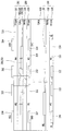
- FIG. 1 is a circuit diagram of a 6T static random access memory
- FIG. 2 illustrates a three-layer organic thin film transistor structure as an example of a stacked structure static random access memory (p type-n type-p type stacked structure)
- FIG. 3 is P It shows a static random access memory in which two type layers and one N type layer are sequentially stacked.
- the 3D static RAM core cell of the vertical stacked structure of the present invention may include a structure in which the first transistor layer 100, the second transistor layer 200, and the third transistor layer 300 are sequentially stacked from the bottom. .
- the transistor layers 100, 200, and 300 each include two pairs of thin film transistors on the same plane.
- the first transistor layer 100 has N-type transistors in pairs on the same plane, and specifically, includes two switching thin film transistors M5 and M6.
- the two switching thin film transistors M5 and M6 independently include a first electrode channel film 110, a first insulating film 120, and a first gate electrode 130 from below.
- the first electrode channel layer 110 may include a first drain electrode 112, a first source electrode 114, and a first organic semiconductor 116.
- the second transistor layer 200 includes N-type transistors in pairs on the same plane, and specifically, includes two storage thin film transistors M1 and M3.
- the two storage thin film transistors M1 and M3 each independently include a second electrode channel film 210, a second insulating film 220, and a second gate electrode 230 from below.
- the second electrode channel film 210 may include a second drain electrode 212, a second source electrode 214, and a second organic semiconductor 216.
- the third transistor layer 300 includes P-type transistors in pairs on the same plane, and specifically, includes two storage thin film transistors M2 and M4.
- the two storage thin film transistors M2 and M4 independently include a third electrode channel film 310, a third insulating film 320, and a third gate electrode 330 from the top.
- the third gate electrode 330 may be the second gate electrode 230
- the third electrode channel layer 310 may include the third drain electrode 312, the third source electrode 314, and the third organic semiconductor.
- 316 may include.
- the first transistor layer 100 and the second transistor layer 200 may further include a first interlayer insulating layer 410 between the first gate electrode 130 and the second electrode channel layer.
- the second interlayer insulating film 420 may be positioned between the second transistor layer 200 and the third transistor layer 300, and the second interlayer insulating film 420 may be the third insulating film 320. Therefore, the second interlayer insulating film 420 may simultaneously serve as the third insulating film 320.
- the second gate electrode 230 may be the third gate electrode 330, and the second gate electrode 230 or the third gate 330 electrode may be the second transistor layer 200 and the third transistor layer, respectively. Since it can be shared by the gate electrode of 300 to perform the role of the gate electrode at the same time, only one of the two (230, 330) can be formed and used.
- the two storage thin film transistors M1 and M3 included in the second transistor layer 200 and the two storage thin film transistors M2 and M4 included in the third transistor layer 300 have a power supply voltage Vdd.
- the data may be written and read by being connected to the ground voltage Vss.
- one switching thin film transistor M5 of the first transistor layer 100 is a bit line pair BL
- the first drain electrode 112 and the first source electrode 114 which are its source and drain electrodes are connected to any one BL, and the first gate electrode which is its gate electrode is connected to the word line WL. 130 may be connected.
- the other switching thin film transistor M6 of the first transistor layer 100 includes a bit line pair BL, Of the other (The first drain electrode 112 and the first source electrode 114, which are its source and drain electrodes, may be connected to each other, and the first gate electrode 130, which is its gate electrode, may be connected to the word line WL. .
- the first transistor layer may be located on a substrate.
- the substrate may be a metal oxide, a semiconductor, glass, plastic, or the like.
- the gate electrode, the source electrode and the drain electrode are each independently Au, Al, Ag, Be, Bi, Co, Cu, Cr, Hf, In, Mn, Mo, Mg, Ni, Nb, Pb, Pd, Pt, Rh , Re, Ru, Sb, Ta, Te, Ti, V, W, Zr, Zn, PEDOT: PSS and the like.
- the vertical connection of the gate electrode, the source and the drain electrode described above may be electrically connected through the conductive via hole.
- the conductive via hole may be filled with a conductive material applied to the gate electrode or the source electrode.
- the thin film transistor may have a flexible property.
- the third transistor layer 300 may include a p-type transistor, and the third organic semiconductor 316 may include a p-type organic semiconductor.
- the p-type organic semiconductor is diF-TES-ADT (2,8-Difluoro-5,11-bis (triethylsilylethynyl) anthradithiophene), pentacene, 3-hexylthiophene polymer (poly (3-hexylthiophene) )), 3-pentylthiophene polymer (poly (3-pentylthiophene)), 3-butylthiophene polymer (poly3- (butylthiophene)), benzodithiophene (benzo [1,2-b: 4,5-b '] dithiophene) polymer, PBDT2FBT-2EHO (poly (4,8-bis (2-ethylhexyloxy) benzo [1,2-b: 4,5-b ′] di thiophene-alt-4,7-bis (4- (2-ethylhexyl) -2-thienyl) -5,6-d
- the first transistor layer 100 and the second transistor layer 200 include n-type transistors, and thus the first organic semiconductor 116 and the second organic semiconductor 216 may each include an n-type organic semiconductor. Can be.
- the n-type organic semiconductor is N2200 (poly ⁇ [N, N'-bis (2-octyldodecyl) -naphthalene-1,4,5,8-bis (dicarboximide) -2,6-diyl] -alt- 5,5 '-(2,2'-bithiophene))), anthracene, tetratracene, hexacene, quinoline, quinolone, naphthylridine, and quinazoline ), Antradithophene, fluorene (fullerene), perylenedicarboximide, naphtalene diimide, oligo-thiophene, 6,13-bis (triisopropyl) Silylethynyl) pentacene) (6,13-Bis (triisopropylsilylethynyl) pentacene), 5,11-bis (triethylsilylethynyny
- the first insulating film 120, the second insulating film 220, the third insulating film 320, the first interlayer insulating film 410, and the second interlayer insulating film 420 include parylene, polydimethylsiloxane, Insulation materials such as PDMS), Cytop (CTL-809M, Asahi Glass), PMMA (poly (methyl methacrylate)), PVP (poly (vinyl pyrrolidone)), PI (polyimide), and aluminum oxide (Al2O3) may be applied.
- the scope of the invention is not limited thereto.
- the present invention provides a static RAM core cell assembly including a plurality of three-dimensional static RAM core cells of the vertically stacked structure on a plane.
- FIG. 4 For reference, an example of the static RAM core cell assembly of the present invention is shown in FIG. 4.
- the present invention provides an electronic device including the three-dimensional static RAM core cell of the vertical stacked structure.
- the electronic device may be applied to various smart electronic products such as computers and wearable devices requiring a semiconductor memory device.
- the first transistor layer 100 including two thin film transistors is formed.
- a second transistor layer 200 is formed on the first transistor layer 100 and includes two thin film transistors.
- a third transistor layer 300 is formed on the second transistor layer 200 and includes two thin film transistors.
- Interlayer electrical connections between the first bit line BL1 and the second bit line BL2 may be connected through a via hole.
- WL word line BL: bit line pair (BL, ) Any one of
- Bit line pair (BL, ) The other one
- Vdd power supply voltage
- Vss ground voltage
- M5 thin film transistors for switching
- first transistor layer 112 first drain electrode
- first source electrode 116 first organic semiconductor
- second source electrode 216 second organic semiconductor
- first interlayer insulating film 420 second interlayer insulating film
- Nano-particle ink (silver-nano particle ink) is printed to apply a source drain electrode on the substrate. Through the heat treatment process, the electrode conductivity was improved and the surface treatment improved the charge injection.
- P-type ink (diF-TES-ADT) dissolved in mesitylene is applied between the source and drain electrodes using a printing process. The heat treatment process evaporates the solvent and improves the properties of the organics. Parylene diX-SR is deposited thereon to form a dielectric layer. The gate electrode is formed thereon by printing nano-particle ink (Silver-nano particle ink).
- First Transistor layer A second transistor layer 200 is formed on the 100 and includes two thin film transistors.
- Nano-particle ink (silver-nano particle ink) was printed and the source drain electrode was applied on the substrate. Through the heat treatment process, the conductivity of the electrode was improved and the surface treatment improved the charge injection.
- the third Transistor layer A third transistor layer 300 is formed on the 200 and includes two thin film transistors.
- Parylene diX-SR was deposited on the shared gate to form a dielectric layer.
- Nano-particle ink (silver-nano particle ink) was printed and the source drain electrode was applied on the substrate.
- the heat treatment process improves the conductivity of the electrode and improves the charge injection by surface treatment.
- P-type ink (diF-TES-ADT) made by dissolving in Mesitylene was applied between the source and drain electrodes using a printing process. The heat treatment process evaporated the solvent and improved the properties of the organics.
- the vias were drilled through the laser and the vias were filled by printing to connect the electrodes between the layers.
- Example 2 three-dimensional Static Including a plurality of core cells Static Fabrication of Core Cell Assemblies
- Example 1 The process of the three-dimensional static RAM core cell manufactured according to Example 1 was applied to an array to prepare a static RAM core cell assembly of 10 rows 10 columns (100).
- the cells in each row share one wordline, and the cells in each column share two bit lines.
- Each line can be formed by printing nanoparticle inks.
- Word lines and bit lines read and write data in each cell.
- Test Example 1 3D Static Core cell Memory performance test
- the memory of the 3-D static RAM core cell of the present invention has excellent static noise margin (SNM) characteristics (about 70% of Vdd / 2) through the butterfly curve of the cross-coupled inverter. It was.
- SNM static noise margin
- the same type of organic transistors are disposed on the same plane and vertically stacked, thereby eliminating a complicated patterning process for forming different types of organic transistors in memory device fabrication.
- the area occupied by the memory device may be reduced to improve the degree of integration of the semiconductor circuit.
Landscapes
- Chemical & Material Sciences (AREA)
- Engineering & Computer Science (AREA)
- Materials Engineering (AREA)
- Semiconductor Memories (AREA)
- Thin Film Transistor (AREA)
- Physics & Mathematics (AREA)
- Geometry (AREA)
Abstract
La présente invention porte sur une cellule centrale RAM statique 3D présentant une structure empilée verticalement, la cellule centrale RAM statique comprenant six transistors en couches minces, dont chacun présente une électrode de grille, une électrode de source et une électrode de drain, la cellule centrale RAM statique comprenant : deux transistors en couches minces servant à la commutation, qui sont connectés chacun à une ligne de bit et à une ligne de mot et qui sélectionnent l'enregistrement et la lecture de données ; et quatre transistors en couches minces servant à la mémorisation de données, qui sont connectés à une tension d'alimentation (Vdd) ou une tension de terre (Vss) et permettent l'enregistrement et la lecture de données, la cellule centrale RAM statique comprenant : une première couche de transistor comprenant deux transistors en couches minces choisis parmi les six transistors en couches minces ; une deuxième couche de transistor qui est positionnée sur la première couche de transistor et comprend deux transistors en couches minces choisis parmi les quatre autres transistors en couches minces ; et une troisième couche de transistor qui est placée sur la deuxième couche de transistor et comprend les autres deux transistors en couches minces, le ou les types d'électrodes de la première couche de transistor et le ou les types d'électrodes de la deuxième couche de transistor étant connectés électriquement, et le ou les types d'électrodes de la deuxième couche de transistor et le ou les types d'électrodes de la troisième couche de transistor étant connectés électriquement. Ainsi, la cellule centrale RAM statique 3D ayant une structure empilée verticalement selon la présente invention permet à un procédé de modélisation complexe de former différents types de transistors organiques à omettre pendant la fabrication d'éléments de mémoire par disposition du même type de transistors organiques sur le même plan et empilement verticalement de ceux-ci et peut améliorer le degré d'intégration d'un circuit semi-conducteur par réduction de la surface occupée par les éléments de mémoire.
Priority Applications (2)
| Application Number | Priority Date | Filing Date | Title |
|---|---|---|---|
| US16/066,862 US10692935B2 (en) | 2015-12-29 | 2016-12-28 | 3D static RAM core cell having vertically stacked structure, and static RAM core cell assembly comprising same |
| CN201680077156.7A CN108431954B (zh) | 2015-12-29 | 2016-12-28 | 具有垂直层叠结构的3d静态ram核心单元的制造方法 |
Applications Claiming Priority (2)
| Application Number | Priority Date | Filing Date | Title |
|---|---|---|---|
| KR1020150188828A KR101855846B1 (ko) | 2015-12-29 | 2015-12-29 | 수직적층구조의 3차원 정적램 코어 셀 및 그를 포함하는 정적램 코어 셀 어셈블리 |
| KR10-2015-0188828 | 2015-12-29 |
Publications (1)
| Publication Number | Publication Date |
|---|---|
| WO2017116143A1 true WO2017116143A1 (fr) | 2017-07-06 |
Family
ID=59225122
Family Applications (1)
| Application Number | Title | Priority Date | Filing Date |
|---|---|---|---|
| PCT/KR2016/015420 Ceased WO2017116143A1 (fr) | 2015-12-29 | 2016-12-28 | Cellule centrale ram statique 3d présentant une structure empilée verticalement, et ensemble cellule centrale ram statique la comprenant |
Country Status (4)
| Country | Link |
|---|---|
| US (1) | US10692935B2 (fr) |
| KR (1) | KR101855846B1 (fr) |
| CN (1) | CN108431954B (fr) |
| WO (1) | WO2017116143A1 (fr) |
Families Citing this family (9)
| Publication number | Priority date | Publication date | Assignee | Title |
|---|---|---|---|---|
| US10658026B2 (en) | 2017-05-26 | 2020-05-19 | Taiwan Semiconductor Manufacturing Company Limited | Word line pulse width control circuit in static random access memory |
| CN109427388B (zh) * | 2017-09-04 | 2020-09-25 | 华为技术有限公司 | 一种存储单元和静态随机存储器 |
| TWI631741B (zh) * | 2017-10-19 | 2018-08-01 | 元太科技工業股份有限公司 | 驅動基板 |
| KR102029963B1 (ko) * | 2018-01-05 | 2019-11-08 | 포항공과대학교 산학협력단 | 센서 증폭 유닛 및 그의 제조방법 |
| US11437376B2 (en) | 2019-05-31 | 2022-09-06 | Tokyo Electron Limited | Compact 3D stacked-CFET architecture for complex logic cells |
| TWI839591B (zh) * | 2019-12-31 | 2024-04-21 | 日商東京威力科創股份有限公司 | 具有三堆疊元件層次的cfet sram位元格 |
| KR102767182B1 (ko) | 2021-09-24 | 2025-02-14 | 한국전자통신연구원 | 산화물 반도체를 포함하는 cmos 로직 소자 |
| US12119060B2 (en) | 2021-09-27 | 2024-10-15 | Samsung Electronics Co., Ltd. | Content-addressable memory and electronic device including the same |
| CN117858494B (zh) * | 2022-09-28 | 2026-01-09 | 华为技术有限公司 | 存储器、电子设备 |
Citations (5)
| Publication number | Priority date | Publication date | Assignee | Title |
|---|---|---|---|---|
| JP2007318106A (ja) * | 2006-04-28 | 2007-12-06 | Semiconductor Energy Lab Co Ltd | 半導体集積回路及びその作製方法、並びに半導体集積回路を用いた半導体装置 |
| KR20080067126A (ko) * | 2007-01-15 | 2008-07-18 | 삼성전자주식회사 | 콘택 구조체들을 갖는 에스램 셀의 제조 방법 |
| KR101100426B1 (ko) * | 2005-05-10 | 2011-12-30 | 삼성전자주식회사 | 단결정 실리콘층을 포함하는 반도체 소자, 이를 포함하는반도체 장치 및 평면표시장치와 반도체 소자의 제조 방법 |
| KR101275758B1 (ko) * | 2007-07-20 | 2013-06-14 | 삼성전자주식회사 | 복수개의 적층된 트랜지스터들을 구비하는 반도체 소자 및그 제조방법 |
| WO2014185085A1 (fr) * | 2013-05-14 | 2014-11-20 | 株式会社 東芝 | Dispositif de stockage à semi-conducteur |
Family Cites Families (3)
| Publication number | Priority date | Publication date | Assignee | Title |
|---|---|---|---|---|
| US6140684A (en) * | 1997-06-24 | 2000-10-31 | Stmicroelectronic, Inc. | SRAM cell structure with dielectric sidewall spacers and drain and channel regions defined along sidewall spacers |
| US7785938B2 (en) * | 2006-04-28 | 2010-08-31 | Semiconductor Energy Laboratory Co., Ltd | Semiconductor integrated circuit, manufacturing method thereof, and semiconductor device using semiconductor integrated circuit |
| JP6013685B2 (ja) * | 2011-07-22 | 2016-10-25 | 株式会社半導体エネルギー研究所 | 半導体装置 |
-
2015
- 2015-12-29 KR KR1020150188828A patent/KR101855846B1/ko active Active
-
2016
- 2016-12-28 CN CN201680077156.7A patent/CN108431954B/zh active Active
- 2016-12-28 US US16/066,862 patent/US10692935B2/en active Active
- 2016-12-28 WO PCT/KR2016/015420 patent/WO2017116143A1/fr not_active Ceased
Patent Citations (5)
| Publication number | Priority date | Publication date | Assignee | Title |
|---|---|---|---|---|
| KR101100426B1 (ko) * | 2005-05-10 | 2011-12-30 | 삼성전자주식회사 | 단결정 실리콘층을 포함하는 반도체 소자, 이를 포함하는반도체 장치 및 평면표시장치와 반도체 소자의 제조 방법 |
| JP2007318106A (ja) * | 2006-04-28 | 2007-12-06 | Semiconductor Energy Lab Co Ltd | 半導体集積回路及びその作製方法、並びに半導体集積回路を用いた半導体装置 |
| KR20080067126A (ko) * | 2007-01-15 | 2008-07-18 | 삼성전자주식회사 | 콘택 구조체들을 갖는 에스램 셀의 제조 방법 |
| KR101275758B1 (ko) * | 2007-07-20 | 2013-06-14 | 삼성전자주식회사 | 복수개의 적층된 트랜지스터들을 구비하는 반도체 소자 및그 제조방법 |
| WO2014185085A1 (fr) * | 2013-05-14 | 2014-11-20 | 株式会社 東芝 | Dispositif de stockage à semi-conducteur |
Also Published As
| Publication number | Publication date |
|---|---|
| CN108431954A (zh) | 2018-08-21 |
| KR20170078373A (ko) | 2017-07-07 |
| CN108431954B (zh) | 2023-04-04 |
| US10692935B2 (en) | 2020-06-23 |
| KR101855846B1 (ko) | 2018-05-09 |
| US20190006424A1 (en) | 2019-01-03 |
Similar Documents
| Publication | Publication Date | Title |
|---|---|---|
| KR101855846B1 (ko) | 수직적층구조의 3차원 정적램 코어 셀 및 그를 포함하는 정적램 코어 셀 어셈블리 | |
| KR101905717B1 (ko) | 삼차원 적층구조의 듀얼 게이트 박막 트랜지스터 논리 회로 | |
| Minari et al. | Room‐temperature printing of organic thin‐film transistors with π‐junction gold nanoparticles | |
| Baeg et al. | Remarkable enhancement of hole transport in top‐gated N‐type polymer field‐effect transistors by a high‐k dielectric for ambipolar electronic circuits | |
| KR100973811B1 (ko) | 유기 반도체를 사용한 박막 트랜지스터 표시판 및 그 제조방법 | |
| Chason et al. | Printed organic semiconducting devices | |
| CN104919596A (zh) | 双极型垂直场效应晶体管 | |
| CN1742393B (zh) | 电子器件及其制造方法 | |
| TW200924173A (en) | An electronic device and a method of manufacturing an electronic device | |
| JP6208133B2 (ja) | 複素環化合物及びその利用 | |
| Tiwari et al. | Complementary-like inverters based on an ambipolar solution-processed molecular bis (naphthalene diimide)-dithienopyrrole derivative | |
| WO2016148460A1 (fr) | Transistor à couches minces à deux grilles | |
| Kim et al. | Static response of three-dimensional and printed complementary organic TFTs-based static random-access memory | |
| Kim et al. | High Mobility Amorphous Polymer‐Based 3D Stacked Pseudo Logic Circuits through Precision Printing | |
| US20240008294A1 (en) | Organic thin film transistor | |
| US8552421B2 (en) | Organic microelectronic device and fabrication method therefor | |
| JP4334907B2 (ja) | 有機電界効果トランジスタ | |
| KR20180058673A (ko) | 수직적층구조의 3차원 정적램 코어 셀 및 그를 포함하는 정적램 코어 셀 어셈블리 | |
| Ni et al. | Superintegrated conformable organic transistors based on a universal microlithographic strategy | |
| KR100925460B1 (ko) | 유기 박막 트랜지스터 기판 및 그 제조 방법 | |
| Khim et al. | Inkjet-printing-based soft-etching technique for high-speed polymer ambipolar integrated circuits | |
| WO2011139006A1 (fr) | Transistor à couches minces organiques ayant une capacité d'injection de charge améliorée, et son procédé de fabrication | |
| KR20150052763A (ko) | 박막 트랜지스터 및 그 제조 방법과 상기 박막 트랜지스터를 포함하는 전자 소자 | |
| Herlogsson | Electrolyte-gated organic thin-film transistors | |
| KR102760164B1 (ko) | 삼차원 적층 구조의 박막 트랜지스터 수도 논리회로 |
Legal Events
| Date | Code | Title | Description |
|---|---|---|---|
| 121 | Ep: the epo has been informed by wipo that ep was designated in this application |
Ref document number: 16882095 Country of ref document: EP Kind code of ref document: A1 |
|
| NENP | Non-entry into the national phase |
Ref country code: DE |
|
| 122 | Ep: pct application non-entry in european phase |
Ref document number: 16882095 Country of ref document: EP Kind code of ref document: A1 |