WO2014185085A1 - Dispositif de stockage à semi-conducteur - Google Patents
Dispositif de stockage à semi-conducteur Download PDFInfo
- Publication number
- WO2014185085A1 WO2014185085A1 PCT/JP2014/051221 JP2014051221W WO2014185085A1 WO 2014185085 A1 WO2014185085 A1 WO 2014185085A1 JP 2014051221 W JP2014051221 W JP 2014051221W WO 2014185085 A1 WO2014185085 A1 WO 2014185085A1
- Authority
- WO
- WIPO (PCT)
- Prior art keywords
- field effect
- type field
- effect transistor
- gate electrode
- effect transistors
- Prior art date
- Legal status (The legal status is an assumption and is not a legal conclusion. Google has not performed a legal analysis and makes no representation as to the accuracy of the status listed.)
- Ceased
Links
Images













Classifications
-
- H—ELECTRICITY
- H10—SEMICONDUCTOR DEVICES; ELECTRIC SOLID-STATE DEVICES NOT OTHERWISE PROVIDED FOR
- H10D—INORGANIC ELECTRIC SEMICONDUCTOR DEVICES
- H10D88/00—Three-dimensional [3D] integrated devices
-
- H—ELECTRICITY
- H10—SEMICONDUCTOR DEVICES; ELECTRIC SOLID-STATE DEVICES NOT OTHERWISE PROVIDED FOR
- H10B—ELECTRONIC MEMORY DEVICES
- H10B10/00—Static random access memory [SRAM] devices
- H10B10/12—Static random access memory [SRAM] devices comprising a MOSFET load element
-
- H—ELECTRICITY
- H10—SEMICONDUCTOR DEVICES; ELECTRIC SOLID-STATE DEVICES NOT OTHERWISE PROVIDED FOR
- H10D—INORGANIC ELECTRIC SEMICONDUCTOR DEVICES
- H10D84/00—Integrated devices formed in or on semiconductor substrates that comprise only semiconducting layers, e.g. on Si wafers or on GaAs-on-Si wafers
- H10D84/01—Manufacture or treatment
- H10D84/0123—Integrating together multiple components covered by H10D12/00 or H10D30/00, e.g. integrating multiple IGBTs
- H10D84/0126—Integrating together multiple components covered by H10D12/00 or H10D30/00, e.g. integrating multiple IGBTs the components including insulated gates, e.g. IGFETs
- H10D84/0165—Integrating together multiple components covered by H10D12/00 or H10D30/00, e.g. integrating multiple IGBTs the components including insulated gates, e.g. IGFETs the components including complementary IGFETs, e.g. CMOS devices
-
- H—ELECTRICITY
- H10—SEMICONDUCTOR DEVICES; ELECTRIC SOLID-STATE DEVICES NOT OTHERWISE PROVIDED FOR
- H10D—INORGANIC ELECTRIC SEMICONDUCTOR DEVICES
- H10D84/00—Integrated devices formed in or on semiconductor substrates that comprise only semiconducting layers, e.g. on Si wafers or on GaAs-on-Si wafers
- H10D84/01—Manufacture or treatment
- H10D84/02—Manufacture or treatment characterised by using material-based technologies
- H10D84/03—Manufacture or treatment characterised by using material-based technologies using Group IV technology, e.g. silicon technology or silicon-carbide [SiC] technology
- H10D84/038—Manufacture or treatment characterised by using material-based technologies using Group IV technology, e.g. silicon technology or silicon-carbide [SiC] technology using silicon technology, e.g. SiGe
Definitions
- Embodiments described herein relate generally to a semiconductor memory device, and more particularly, to an SRAM (Static Random Access).
- the present invention relates to a semiconductor memory device having a three-dimensional structure.
- SNM Static Noise Margin
- SRAM Static Noise Margin
- SNM represents the upper limit of the magnitude of noise that is not lost in stored information. If the SNM is zero, the upper limit of the magnitude of the noise that is not lost in the stored information is zero, that is, the stored information is lost in any noise. That means that no noise is allowed, so such SRAM cannot be used.
- the SNM decreases as the power supply voltage decreases. Therefore, the reduction of the power supply voltage has been restricted due to the decrease of the SNM accompanying the reduction of the power supply voltage.
- the problem to be solved by the present invention is to provide a semiconductor memory device capable of increasing the SNM under a constant power supply voltage in an SRAM structure.
- a semiconductor memory device is formed on a semiconductor substrate, first and second p-type field effect transistors and first and second n-type field effect transistors formed on the semiconductor substrate, and the respective transistors. And the third and fourth n-type field effect transistors formed on the insulating film.
- Each source region and each substrate electrode of the first and second p-type field effect transistors are connected to a wiring whose potential is maintained at a power supply voltage, and each of the first and second n-type field effect transistors is The source region and each substrate electrode are connected to a wiring whose potential is maintained at the ground potential, and each drain region of the first p-type field effect transistor and the first n-type field effect transistor and the second p-type
- the gate electrodes of the n-type field effect transistor and the second n-type field effect transistor and the drain region of the third n-type field effect transistor are connected to each other, and the second p-type field effect transistor and the second n-type field effect transistor Each n-type field effect transistor drain region, the first p-type field effect transistor, each gate electrode of the first n-type field effect transistor, and the fourth n-type.
- a drain region of the field effect transistor is connected to each other, gate electrodes of the third and fourth n-type field effect transistors are connected to a word line, and a source region of the third n-type field effect transistor is a bit And a source region of the fourth n-type field effect transistor is connected to an inverted bit line.
- the third and fourth n-type field effect transistors have a planar structure, and at least a part of the channel region of the third n-type field effect transistor is a gate of the second p-type field effect transistor.
- An electrode and a wiring connected to the gate electrode overlap with at least a part of the gate electrode of the second n-type field effect transistor and the wiring connected to the gate electrode when viewed from the normal direction of the semiconductor substrate.
- the channel region of the fourth n-type field effect transistor includes a gate electrode of the first p-type field effect transistor, a wiring connected to the gate electrode, and the first n-type field effect transistor. Formed so as to overlap at least a part of the gate electrode of the type field effect transistor and the wiring connected to the gate electrode when viewed from the normal direction of the semiconductor substrate It has been.
- At least one of the field effect transistors constituting the SRAM is formed on the field effect transistor forming the storage node via an insulating film.
- at least one threshold voltage of the field effect transistor constituting the inverter whose output terminal is the potential of the power supply voltage among the two sets of inverters constituting the SRAM is positive.
- the threshold voltage of the field effect transistor connecting the output terminal of the inverter and the bit line or the inverted bit line changes in the negative direction.
- the threshold voltage of at least one of the field effect transistors constituting the inverter of which the output terminal is at the ground potential among the two sets of inverters constituting the SRAM changes in the negative direction, or the output terminal of the inverter
- the threshold voltage of the field effect transistor connecting the bit line or the inverted bit line changes in the positive direction.
- FIG. 1 is a circuit configuration diagram showing the semiconductor memory device according to the first embodiment.
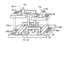
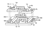
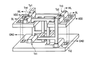
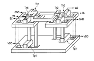
- FIG. 2 is a bird's-eye view showing a schematic structure of the semiconductor memory device according to the first embodiment.
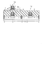
- FIG. 3 is a cross-sectional view showing a schematic structure of the semiconductor memory device according to the first embodiment.
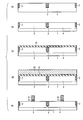
- FIG. 4 is a cross-sectional view showing a manufacturing process of the semiconductor memory device according to the first embodiment.
- FIG. 5 is a cross-sectional view showing a manufacturing process of the semiconductor memory device according to the first embodiment.
- FIG. 6 is a cross-sectional view showing the manufacturing process of the semiconductor memory device according to the first embodiment.
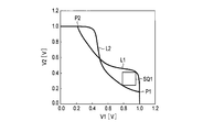
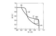
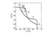
- FIG. 7 is a characteristic diagram showing a butterfly curve when there is no variation in the threshold voltage, for explaining the performance of the semiconductor memory device according to the first embodiment.
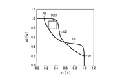
- FIG. 8A is a characteristic diagram for explaining the performance of the semiconductor memory device according to the first embodiment and showing a butterfly curve when the threshold voltage varies.
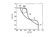
- FIG. 8B is a characteristic diagram illustrating a butterfly curve when the threshold voltage varies in order to explain the performance of the semiconductor memory device according to the first embodiment.
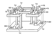
- FIG. 9 is a bird's-eye view showing the structure of the first modification of the first embodiment.
- FIG. 10 is a cross-sectional view showing the manufacturing process of the first modification of the first embodiment.
- FIG. 11 is a bird's-eye view showing the structure of the second modification of the first embodiment.
- FIG. 12 is a bird's-eye view showing the structure of the third modification of the first embodiment.
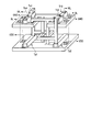
- FIG. 13 is a bird's-eye view showing a schematic structure of the semiconductor memory device according to the second embodiment.
- FIG. 14A is a characteristic diagram for explaining the performance of the semiconductor memory device according to the second embodiment.
- FIG. 14B is a characteristic diagram for explaining the performance of the semiconductor memory device according to the second embodiment.
- FIG. 15 is a bird's eye view showing a schematic structure of a semiconductor memory device according to a modification of the second embodiment.
- FIG. 16A is a characteristic diagram for explaining the performance of the semiconductor memory device according to the modification of the second embodiment.
- FIG. 16B is a characteristic diagram for explaining the performance of the semiconductor memory device according to the modification of the second embodiment.
- FIG. 16A is a characteristic diagram for explaining the performance of the semiconductor memory device according to the modification of the second embodiment.
- FIG. 16B is a characteristic diagram for explaining the performance of the semiconductor memory device according to the modification of the second
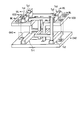
- FIG. 17 is a bird's-eye view showing a schematic structure of the semiconductor memory device according to the third embodiment.
- FIG. 18A is a characteristic diagram for explaining the performance of the semiconductor memory device according to the third embodiment.
- FIG. 18B is a characteristic diagram for explaining the performance of the semiconductor memory device according to the third embodiment.
- FIG. 19 is a bird's-eye view showing a schematic structure of a semiconductor memory device according to a modification of the third embodiment.
- FIG. 20A is a characteristic diagram for explaining the performance of the semiconductor memory device according to the modification of the third embodiment.
- FIG. 20B is a characteristic diagram for explaining the performance of the semiconductor memory device according to the modification of the third embodiment.
- FIG. 21 is a bird's-eye view showing a schematic structure of the semiconductor memory device according to the fourth embodiment.
- FIG. 22 is a bird's-eye view showing a schematic structure of a semiconductor memory device according to a modification of the fourth embodiment.
- FIG. 23 is a bird's-eye view showing a schematic structure of the semiconductor memory device according to the fifth embodiment.
- FIG. 24 is a bird's-eye view showing a schematic structure of a semiconductor memory device according to a modification of the fifth embodiment.
- FIG. 1 is a circuit configuration diagram showing a semiconductor memory device according to the first embodiment of the present invention.
- VDD is at the power supply voltage.
- GND represents a wiring whose potential is maintained at the ground potential
- WL represents a word line
- BL represents a bit line
- BL ′ represents an inverted bit line.
- the substrate electrode of the field effect transistor is omitted.
- FIG. 2 schematically shows the structure of the first embodiment in a bird's-eye view.
- the thickness of the semiconductor layer on which the field effect transistor formed on the insulating film formed on the semiconductor substrate is omitted, and the interlayer insulating film thereon is also omitted.
- the substrate electrode of the field effect transistor formed on the semiconductor substrate is omitted.
- the distance between the field effect transistor formed on the semiconductor substrate and the field effect transistor formed on the insulating film in the direction perpendicular to the surface of the semiconductor substrate is enlarged. . In general, the scale of the figure is not accurate.
- first and second p-type field effect transistors Tp1 and Tp2 and first and second n-type field effect transistors Tn1 and Tn2 are formed on a semiconductor substrate.
- Third and fourth n-type field effect transistors Tn3 and Tn4 are formed on the insulating film formed above.
- the channel region of the third n-type field effect transistor Tn3 is formed so as to overlap the gate electrode of the second p-type field effect transistor Tp2 when viewed from the normal direction of the semiconductor substrate.
- the channel region of the field effect transistor Tn4 is formed so as to overlap the gate electrode of the first p-type field effect transistor Tp1 when viewed from the normal direction of the semiconductor substrate.
- the normal direction is a direction perpendicular to the surface of the semiconductor substrate.
- FIG. 3 schematically shows a cross-sectional structure of the present embodiment.
- a cross section of only the first p-type field effect transistor Tp1 and the first and fourth n-type field effect transistors Tn1 and Tn4 is schematically shown as if they were formed in the same direction. Also, the scale of the figure is not accurate. Further, the wiring or the interlayer insulating film of the second layer or higher is omitted.
- an element isolation region 2 made of, for example, silicon oxide is formed in a semiconductor substrate 1 made of, for example, silicon, and an n-well region 3 and a p-well region 4 are formed in regions separated by the element isolation region 2.
- a gate electrode 6 is formed on each of the n well region 3 and the p well region 4 with a gate insulating film 5 interposed therebetween.
- a source / drain region 7 is formed so as to sandwich the gate electrode 6, and a gate sidewall 8 is formed in contact with the gate electrode.
- the first p-type field effect transistor Tp1 is formed in the n-well region 3, and the first n-type field-effect transistor Tn1 is formed in the p-well region 4, respectively.
- An interlayer insulating film 9 made of, for example, silicon oxide is formed on the first p-type field effect transistor Tp1 and the first n-type field effect transistor Tn1, and made of, for example, silicon.
- a semiconductor layer 10 containing p-type impurities is formed.
- a gate electrode 6 is formed on the semiconductor layer 10 with a gate insulating film 5 interposed therebetween.
- a source / drain region 7 is formed in the semiconductor layer 10 so as to sandwich the gate electrode 6, and a gate sidewall 8 is formed in contact with the gate electrode, so that the fourth n-type field effect transistor Tn 4 is formed. Is formed.
- the channel region 11 formed between the source / drain regions 7 of the fourth n-type field effect transistor Tn4 is a gate electrode of the first p-type field effect transistor Tp1 when viewed from the normal direction of the semiconductor substrate 1. 6 is formed so as to overlap.
- a second p-type field effect transistor Tp2 and second and third n-type field effect transistors Tn2 and Tn3 are also formed, and the third n-type field effect transistor Tn3 is also formed.
- the channel region is formed so as to overlap the gate electrode of the second p-type field effect transistor Tp2 when viewed from the normal direction of the semiconductor substrate 1.
- an element isolation region 2 is formed on a silicon substrate 1 by a method such as shallow trench isolation (STI).
- STI shallow trench isolation
- As arsenic
- B boron
- a thermal process is performed to form n well region 3 and p well region 4. It is possible to introduce an impurity only into a specific region by using a method such as a photo-etching method or a lithography process.
- an HfO 2 film 12 having a thickness of 5 nm is formed on the semiconductor substrate 1 by a method such as chemical vapor deposition.
- a tungsten film 13 having a thickness of 50 nm is formed by a method such as chemical vapor deposition.
- a part of the tungsten film 13 is selectively removed by performing a process such as an active ion etching method to form the gate electrode 6.
- a part of the HfO 2 film 12 is selectively removed by performing a process such as an active ion etching method, and the gate insulating film 5 is formed.
- B is implanted into the p-type field effect transistor formation region, and As is implanted into the n-type field effect transistor formation region, the extension region 14 is formed.
- a silicon oxide film (not shown) having a thickness of 20 nm is formed by a method such as chemical vapor deposition. Subsequently, a part of the silicon oxide film is selectively removed by etching back by, for example, an active ion etching method, and the gate sidewall 8 is formed.
- B is implanted into the p-type field effect transistor formation region.
- As is implanted into the n-type field effect transistor formation region, and a thermal process is performed.
- source / drain regions 7 are formed.
- a silicon oxide film (not shown) having a thickness of 100 nm is formed on the entire surface of the semiconductor substrate 1 by a method such as chemical vapor deposition, and planarization is performed.
- the interlayer insulating film 9 is formed.
- illustration is abbreviate
- a 20 nm thick silicon layer (not shown) containing B is formed on the interlayer insulating film 9 by a method such as chemical vapor deposition, for example.
- Element isolation is performed by a method such as a mesa element isolation method to form the semiconductor layer 10.
- an HfO 2 film (not shown) having a thickness of 5 nm is formed on the semiconductor layer 10 by a method such as chemical vapor deposition.
- a 50 nm-thickness tungsten film (not shown) is formed on the HfO 2 film (not shown) by a method such as chemical vapor deposition.
- a part of the tungsten film (not shown) is selectively removed, for example, by performing a process such as an active ion etching method, and the gate electrode 6 is formed.
- the gate insulating film 5 is formed by selectively removing a part of the HfO 2 film (not shown) by, for example, active ion etching.
- an extension region 14 is formed in the surface portion of the semiconductor layer 10 by implanting, for example, As.
- a silicon oxide film (not shown) having a thickness of 20 nm is formed by a method such as chemical vapor deposition.
- a part of the silicon oxide film is selectively removed by etching back by, for example, an active ion etching method, and the gate sidewall 8 is formed.
- the source / drain region 7 is formed together with the extension region 14 by performing a thermal process. Thereafter, the structure shown in FIG. 3 is formed through an interlayer insulating film forming process, a wiring process, and the like in the same manner as the prior art.
- a semiconductor memory device is formed using a bulk substrate
- a semiconductor substrate in which a semiconductor layer is formed on a support substrate via an insulating film.
- a semiconductor memory device can be formed, and similar effects can be obtained.
- an element is formed using a semiconductor substrate having the above structure
- the same effect can be obtained by forming an element having a structure in which gate electrodes are provided above and below a channel region in an element formed on a semiconductor layer. It is done.
- Such a structure is preferable because controllability of the gate electrode with respect to the potential of the channel region can be improved.
- a planar structure element is shown as an example.
- a triple gate Triple Gate
- Similar effects can be obtained in the case of a three-dimensional element such as a structure, a gate all around structure, and a vertical structure. It is preferable to form a semiconductor memory device using an element having such a structure because the controllability of the gate electrode with respect to the potential of the channel region can be improved.
- the formation process of only a single semiconductor memory device is shown.
- active elements such as a field effect transistor, a bipolar transistor, and a single electron transistor
- the present invention can also be used when a semiconductor memory device is formed as a part of a semiconductor device including a passive element such as a resistor, a diode, an inductor, a capacitor, or an element using a magnetic material, for example.
- a passive element such as a resistor, a diode, an inductor, a capacitor, or an element using a magnetic material, for example.
- OEIC Optical Electrical Integrated Circuit
- MEMS Micro Electro Mechanical System
- Another group V impurity may be used as an impurity for forming the region, or another group III impurity may be used as an impurity for forming the p-type semiconductor region.
- the introduction of Group III or Group V impurities may be carried out in the form of a compound containing them.
- the introduction of impurities into the source / drain regions is performed using ion implantation, but may be performed using a method other than ion implantation such as solid phase diffusion or vapor phase diffusion. Furthermore, a method of depositing or growing a semiconductor containing impurities may be used.
- the ion implantation method is used, there is an advantage that it is easy to form a complementary semiconductor device including an n-type semiconductor element and a p-type semiconductor element.
- impurities are introduced using a method such as vapor phase diffusion, there is an advantage that it is easy to realize a high impurity concentration.
- a stressor may be formed on the source / drain regions. It is preferable to apply strain to the channel region in this manner because the mobility of current carriers is improved.
- the present embodiment has an advantage that the process can be simplified.
- silicon is used as a semiconductor layer for forming an element.
- the semiconductor layer is not limited to silicon, and germanium or a mixed crystal of silicon and germanium may be used. Germanium or a mixed crystal of silicon and germanium is preferable because it has an advantage of higher mobility of current carriers than silicon.
- a semiconductor that is a compound of a group III element and a group V element may be used as a semiconductor layer forming the element.
- Such compounds are also preferred because they have the advantage of higher current carrier mobility than silicon.
- InAs indium arsenide
- In x Ga 1-x As (0 ⁇ x ⁇ 1) indium gallium arsenide
- InSb indium antimony
- the conventional manufacturing process can be used as it is, which has another advantage that the manufacturing process can be easily constructed.
- the source / drain regions are formed after the processing of the gate electrode and the gate insulating film.
- the order is not essential, and the order may be reversed.
- the gate electrode is formed using tungsten, but may be formed using another metal.
- a semiconductor such as single crystal silicon or amorphous silicon, a compound containing a metal, or a stacked layer thereof may be used.
- a gate electrode is formed using a semiconductor, there is an advantage that the threshold voltage can be easily controlled.
- a complementary semiconductor device is formed, either an n-type semiconductor element or a p-type semiconductor element is used.
- it is preferable to form the gate electrode using a metal or a compound containing a metal because resistance of the gate electrode is suppressed, so that high-speed operation of the device can be obtained.
- the gate electrode is formed of metal, the oxidation reaction does not proceed easily, so that there is an advantage that the interface controllability such as suppression of the level at the interface between the gate electrode and the insulating film is good.
- the gate electrode is formed using a method in which anisotropic etching is performed after depositing the material.
- a method such as embedding such as a damascene process is used. May be formed.
- it is preferable to use a damascene process because the source / drain regions and the gate electrode are formed in a self-aligned manner.
- the length of the gate electrode measured in the main direction of the current flowing through the element is equal to the upper part and the lower part of the gate electrode, but this is not essential.
- the length of the upper part of the gate electrode measured in the shape of an alphabet “T” may be longer than the length measured in the lower part. In this case, there is an advantage that the gate resistance can be reduced.
- a silicide or germanide layer or the like may be formed on the source / drain region.
- a method of depositing or growing a layer containing a metal on the source / drain regions may be used. This is preferable because the resistance of the source / drain regions is reduced.
- the gate electrode is formed of polycrystalline silicon or the like, a process such as silicide or germanide may be performed on the gate electrode. In that case, it is preferable to perform a process such as silicide or germanide because the gate resistance is reduced. Further, an elevator structure may be used. The elevated structure is also preferable because the resistance of the source / drain regions is reduced.
- the upper part of the gate electrode has a structure in which the electrode is exposed, but an insulator such as silicon oxide, silicon nitride, or silicon oxynitride may be provided on the upper part.
- an insulator such as silicon oxide, silicon nitride, or silicon oxynitride may be provided on the upper part.
- the gate electrode is formed of a material containing metal and a silicide or germanide layer or the like is formed on the source / drain region, the gate electrode needs to be protected during the manufacturing process, etc. It is essential to provide a protective material such as silicon oxide, silicon nitride, or silicon oxynitride on the gate electrode.
- the HfO 2 film is used as the gate insulating film.
- an insulating film such as a silicon oxide film or a silicon oxynitride film, or another insulating film such as a stacked layer thereof may be used.
- nitrogen is present in the insulating film, when polycrystalline silicon containing impurities is used as the gate electrode, it is suppressed that the impurities are diffused into the substrate, so that variation in threshold voltage is suppressed. This is preferable because of its advantages.
- silicon oxide there is an advantage that variation in device characteristics is suppressed because there are few interface states at the interface with the gate electrode or fixed charges in the insulating film.
- an oxide of a certain substance when used as the insulating film, a method of first forming a film of the substance and oxidizing it may be used. Moreover, you may expose to the oxygen gas of the excited state which does not necessarily accompany temperature rising. Forming by using a method of exposing to an excited oxygen gas that is not accompanied by an increase in temperature is preferable because impurities in the channel region can be prevented from changing the concentration distribution due to diffusion.
- a silicon oxide film may be formed, and then nitrogen may be introduced into the insulating film by exposure to a gas containing nitrogen in a heated or excited state. Forming by using a method of exposing to an excited nitrogen gas that is not accompanied by an increase in temperature is preferable because the concentration distribution of the impurities in the channel region can be suppressed by diffusion.
- a silicon nitride film may be formed, and then oxygen may be introduced into the insulating film by exposure to a gas containing oxygen in a heated or excited state. Forming by using a method of exposing to an excited oxygen gas that is not accompanied by an increase in temperature is preferable because impurities in the channel region can be prevented from changing the concentration distribution due to diffusion.
- Hf hafnium
- Zr zirconium
- Ti titanium
- Sc scandium
- Y yttrium
- Ta tantalum
- Al aluminum
- La lanthanum
- Ce ce
- Pr Pr
- insulating films containing nitrogen in them.
- Other insulating films such as a body film or a laminate thereof may be used.
- the method for forming the insulating film is not limited to the chemical vapor deposition method, and other methods such as a thermal oxidation method, a vapor deposition method, a sputtering method, or an epitaxial growth method may be used.
- post-oxidation after the formation of the gate electrode is not mentioned, but a post-oxidation step may be performed if possible in view of the material of the gate electrode.
- the process is not necessarily limited to post-oxidation, and a process of rounding the corners of the gate electrode may be performed using a method such as chemical treatment or exposure to a reactive gas. If these steps are possible, the electric field at the lower end corner of the gate electrode is relaxed, which improves the reliability of the gate insulating film, which is preferable.
- the silicon oxide film is used as the interlayer insulating film.
- a substance other than silicon oxide such as a low dielectric constant material may be used for the interlayer insulating film. If the dielectric constant of the interlayer insulating film is set low, there is an advantage that high-speed operation of the device can be obtained because the parasitic capacitance of the device is reduced.
- contact holes it is possible to form self-aligned contacts.
- the use of the self-aligned contact is preferable because the area of the element can be reduced, and the degree of integration can be improved.
- the formation of the metal layer for wiring may be performed using, for example, a sputtering method or a method such as a deposition method. Furthermore, a method such as selective growth of metal may be used, or a method such as damascene method may be used. Further, as the material of the wiring metal, for example, Al (aluminum) containing silicon may be used, or a metal such as Cu (copper) may be used. In particular, Cu is preferable because of its low resistivity.
- the semiconductor layer formed on the interlayer insulating film may be crystallized. Since crystallization increases the carrier mobility, there is an advantage that the operation speed can be improved.
- the schematic diagram of the structure of this embodiment is merely an example, and the arrangement of the field effect transistor in the direction perpendicular to the surface of the semiconductor substrate is essential, but the arrangement in the direction parallel to the surface of the semiconductor substrate is essential. is not. Even if other arrangements are used, the same effect can be obtained. Also, the arrangement or shape of the wiring is not essential, and the same effect can be obtained with other arrangements or shapes as long as the connection relationship is maintained.
- the gate length of the element is 25 nm
- the first and second p-type field effect transistors Tp1 and Tp2 have the same characteristics
- the first to fourth n-type field effect transistors Tn1 to Tn4 are all the same. It was set as the element of the characteristic.
- the gate insulating film was made of silicon oxide having a thickness of 1 nm.
- Fig. 7 shows the butterfly curve (Butterfly Curve) when there is no fluctuation in the threshold voltage.
- the drain region of the first p-type field effect transistor Tp1 the drain region of the first n-type field effect transistor Tn1
- the gate electrode of the second p-type field effect transistor Tp2 the second n-type.
- the potential at the connection point between the gate electrode of the n-type field effect transistor Tn2 and the drain region of the third n-type field effect transistor Tn3 is V1
- the drain region of the second p-type field effect transistor Tp2 is The drain region of the second n-type field effect transistor Tn2, the gate electrode of the first p-type field effect transistor Tp1, the gate electrode of the first n-type field effect transistor Tn1, and the drain region of the fourth n-type field effect transistor Tn4
- V2 The potential at the connection point connected to each other is denoted as V2.
- the potential of the bit line BL is the power supply voltage
- the potential of the inverted bit line BL ′ is the ground potential
- the potential of the bit line BL, the potential of the inverted bit line BL ′, and the potential of the word line WL V1 and V2 are P1 in the figure.
- the potential of the bit line BL is set to the ground potential and the potential of the inverted bit line BL ′ is set to the power supply voltage at the time of writing, and the potential of the bit line BL, the potential of the inverted bit line BL ′, and the potential of the word line WL after the writing.
- V1 and V2 become P2 in the figure.
- the shape of the butterfly curve changes due to noise, and when the closed curve of L1 in the figure disappears, the state of P1 becomes unstable and becomes the state of P2 regardless of whether the previous state was P1 or P2. Also, the shape of the butterfly curve changes due to noise, and when the closed curve of L2 in the figure disappears, the state of P2 becomes unstable and becomes the state of P1 regardless of whether the previous state was P1 or P2. That is, in any case, the stored information is lost. Therefore, the larger the closed curve of L1 or L2, the larger the upper limit of the magnitude of noise that does not lose information.
- An index indicating the upper limit is the above-described SNM, and a specific value is included in L1 or L2 and the side is the largest of the squares parallel to the vertical and horizontal axes in the figure, that is, SQ1 or SQ2 respectively. Is given by the length of the side.
- the SNM indicating the stability of P1 ie, the length of the side of SQ1
- the SNM indicating the stability of P2 ie, the length of the side of SQ2
- the second p-type is compared with the threshold voltage of the fourth n-type field effect transistor Tn4 in which the channel region is formed on the gate electrode of the first p-type field effect transistor Tp1.
- the threshold voltage of the third n-type field effect transistor Tn3 where the channel region is formed on the gate electrode of the field effect transistor Tp2 changes in the negative direction.
- the threshold voltage of the third n-type field effect transistor Tn3 changes by 50 mV in the negative direction as compared with the case shown in FIG. 7, and the threshold of the fourth n-type field effect transistor Tn4 is changed.
- a butterfly curve was calculated on the assumption that the value voltage was changed by 50 mV in the positive direction.
- the threshold voltage in the case where there is no change is adjusted so that the threshold voltage of the both becomes the value described here as a result of the change.
- the results are shown in FIG. 8A.
- the closed curve L1 is larger, and accordingly, the square SQ1 representing the SNM indicating the stability of P1 is also larger. I understand.
- the specific value of SNM in this case is 0.170V.
- the first p-type is compared with the threshold voltage of the third n-type field effect transistor Tn3 in which the channel region is formed on the gate electrode of the second p-type field effect transistor Tp2.
- the threshold voltage of the fourth n-type field effect transistor Tn4 where the channel region is formed on the gate electrode of the field effect transistor Tp1 changes in the negative direction.
- the threshold voltage of the third n-type field effect transistor Tn3 changes by 50 mV in the positive direction as compared with the case shown in FIG. 7, and the threshold of the fourth n-type field effect transistor Tn4 is changed.
- the butterfly curve was calculated on the assumption that the value voltage was changed by 50 mV in the negative direction.
- the threshold voltage in the case where there is no change is adjusted so that the threshold voltage of the both becomes the value described here as a result of the change.
- FIG. 8B In this case, it becomes a curve in which the vertical axis and the horizontal axis of the butterfly curve shown in FIG. 8A are interchanged. Compared to the case where there is no change in the threshold voltage shown in FIG.
- the closed curve L2 is larger, and accordingly, the square SQ2 representing the SNM indicating the stability of P2 is also larger.
- the specific value of the SNM in this case is 0.170 V, which is the same as that shown in FIG. 8A.
- the semiconductor memory device of this embodiment has an increased SNM, that is, improved resistance to noise. I know that.
- the SNM is increased in the semiconductor memory device of this embodiment is that the channel regions of the third and fourth n-type field effect transistors Tn3 and Tn4 are the second and first p-type electric fields, respectively.
- the gate electrodes of the second and first p-type field effect transistors Tp2 and Tp1 are effectively third and fourth n-type, respectively. It is to act as the back gate electrode of the field effect transistors Tn3 and Tn4.
- the channel regions of the third and fourth n-type field effect transistors Tn3 and Tn4 are formed so as to overlap the gate electrodes of the second and first p-type field effect transistors Tp2 and Tp1, respectively. If the fourth n-type field effect transistors Tn3 and Tn4 have a structure other than a planar structure such as a columnar structure, the threshold voltage does not change, so the effect of the present embodiment cannot be obtained. Therefore, it is essential that the third and fourth n-type field effect transistors Tn3 and Tn4 have a planar structure.
- the channel regions of the third and fourth n-type field effect transistors Tn3 and Tn4 are formed so as to overlap the gate electrodes of the second and first p-type field effect transistors Tp2 and Tp1, respectively.
- the increase in the SNM is essential because the gate electrodes of the second and first p-type field effect transistors Tp2 and Tp1 are effectively third and fourth n respectively.
- the channel regions of the third and fourth n-type field effect transistors Tn3 and Tn4 are not necessarily formed so as to overlap the gate electrodes of the second and first p-type field effect transistors Tp2 and Tp1, respectively. The same effect can be obtained even if they are formed so as to overlap with the wirings connected to the gate electrodes of the second and first p-type field effect transistors Tp2 and Tp1, respectively.
- the essence of increasing the SNM in the semiconductor memory device of this embodiment is that the gate electrodes of the second and first p-type field effect transistors Tp2 and Tp1 are effectively third and fourth, respectively.
- the threshold voltage of the third and fourth n-type field effect transistors Tn3 and Tn4 has changed as a result of acting as the back gate electrodes of the n-type field effect transistors Tn3 and Tn4.
- There is fluctuation in the electric potential at normal temperature which is the thermal potential, ie, kT / q (k is Boltzmann's constant, T is 300 K at absolute temperature, ie, normal temperature, q is elementary charge, ie, 1.6 ⁇ 10 ⁇ 19 C, kT / q.
- the change in threshold voltage accompanying the application of the voltage to the back gate electrode was calculated.
- 1 V of the assumed power supply voltage to the back gate electrode In order to obtain a change amount of the threshold voltage of 78 mV, it has been found that the thickness of the insulating film between the channel region and the back gate electrode needs to be 70 nm or less. Therefore, it is formed on the insulating film among the lower end of the channel region of the field effect transistor formed on the insulating film and the gate electrode of the field effect transistor formed on the semiconductor substrate and the wiring connected to the gate electrode.
- the distance measured in the direction perpendicular to the surface of the semiconductor substrate between the upper end of the region overlapping the channel region of the field effect transistor is preferably 70 nm or less.
- a voltage of 1V ⁇ 0.18V 0.82V, which is a difference in gate voltage value of the field effect transistor formed on the semiconductor substrate, is applied to the back gate electrode.
- the thickness of the insulating film between the channel region and the back gate electrode needs to be 40 nm or less in order to obtain a change in threshold voltage of 78 mV. Therefore, it is formed on the insulating film among the lower end of the channel region of the field effect transistor formed on the insulating film and the gate electrode of the field effect transistor formed on the semiconductor substrate and the wiring connected to the gate electrode. More preferably, the distance measured in the direction perpendicular to the surface of the semiconductor substrate with respect to the upper end of the region overlapping the channel region of the field effect transistor is 40 nm or less.
- the semiconductor memory device of this modification has the same circuit as that of the first embodiment shown in FIG. 1, but has a different three-dimensional structure. That is, in this modification, as schematically shown in FIG. 9, the first and second p-type field effect transistors Tp1, Tp2 and the first and second n-type field effect transistors Tn1 are formed on the semiconductor substrate. , Tn2 are formed, and third and fourth n-type field effect transistors Tn3, Tn4 are formed on the insulating film formed thereon.
- the channel region of the third n-type field effect transistor Tn3 is formed so as to overlap the gate electrode of the second n-type field effect transistor Tn2 when viewed from the normal direction of the semiconductor substrate.
- the channel region of the field effect transistor Tn4 is formed so as to overlap the gate electrode of the first n-type field effect transistor Tn1 when viewed from the normal direction of the semiconductor substrate.
- B is formed on the interlayer insulating film 9 by a method such as chemical vapor deposition.
- a silicon layer (not shown) having a thickness of 20 nm including is formed, and element isolation is performed by a method such as a mesa element isolation method to form the semiconductor layer 10.
- an HfO 2 film (not shown) having a thickness of 5 nm is formed on the semiconductor layer 10 by a method such as chemical vapor deposition.
- a 50 nm thick tungsten film (not shown) is formed on the HfO 2 film (not shown) by a method such as chemical vapor deposition.
- a part of the tungsten film (not shown) is selectively removed by subjecting the tungsten film (not shown), for example, to a gate electrode 6.
- a part of the HfO 2 film (not shown) is selectively removed, for example, by performing a process such as an active ion etching method to form the gate insulating film 5.
- the extension region 14 is formed in the surface portion of the semiconductor layer 10 by implanting, for example, As. Subsequently, a silicon oxide film (not shown) having a thickness of 20 nm is formed by a method such as chemical vapor deposition. Thereafter, a part of the silicon oxide film is selectively removed by etching back using a method such as an active ion etching method, and the gate sidewall 8 is formed.
- a silicon oxide film (not shown) having a thickness of 20 nm is formed by a method such as chemical vapor deposition. Thereafter, a part of the silicon oxide film is selectively removed by etching back using a method such as an active ion etching method, and the gate sidewall 8 is formed.
- the semiconductor memory device having the structure shown in FIG. 9 is formed through an interlayer insulating film forming process or a wiring process in the same manner as in the prior art.
- the gate electrode of the first n-type field effect transistor Tn1 and the gate electrode of the first p-type field effect transistor Tp1 are connected to each other, and the gate electrode of the second n-type field effect transistor Tn2 is connected to the second p-type field effect transistor Tn2.
- the gate electrode of the type field effect transistor Tp2 is mutually connected. Therefore, the gate electrode of the first n-type field effect transistor Tn1 and the gate electrode of the first p-type field effect transistor Tp1 are at the same potential, and the gate electrode of the second n-type field effect transistor Tn2 And the gate electrode of the second p-type field effect transistor Tp2 have the same potential.
- the semiconductor memory device of this modification can achieve the same effects as those of the semiconductor memory device of the above embodiment.
- the semiconductor memory device of this modification has the same circuit as that of the first embodiment shown in FIG. 1, but has a different three-dimensional structure. That is, in this modification, as schematically shown in FIG. 11, the first and second p-type field effect transistors Tp1, Tp2 and the first and second n-type field effect transistors Tn1 are formed on the semiconductor substrate. , Tn2 are formed, and third and fourth n-type field effect transistors Tn3, Tn4 are formed on the insulating film formed thereon.
- the channel region of the third n-type field effect transistor Tn3 is formed so as to overlap the gate electrode of the second p-type field effect transistor Tp2 when viewed from the normal direction of the semiconductor substrate.
- the channel region of the field effect transistor Tn4 is formed so as to overlap the gate electrode of the first n-type field effect transistor Tn1 when viewed from the normal direction of the semiconductor substrate.
- the manufacturing process of the semiconductor memory device according to the present modification is essentially the same as the manufacturing process according to the first embodiment or the first modification, and a description thereof will be omitted.
- the gate electrode of the first n-type field effect transistor Tn1 and the gate electrode of the first p-type field effect transistor Tp1 are connected to each other, and the gate electrode of the second n-type field effect transistor Tn2 is connected to the second p-type field effect transistor Tn2.
- the gate electrode of the type field effect transistor Tp2 is mutually connected. Therefore, the gate electrode of the first n-type field effect transistor Tn1 and the gate electrode of the first p-type field effect transistor Tp1 are at the same potential, and the gate electrode of the second n-type field effect transistor Tn2 And the gate electrode of the second p-type field effect transistor Tp2 have the same potential.
- the semiconductor memory device of this modification can achieve the same effects as those of the semiconductor memory device of the above embodiment.
- the semiconductor memory device of this modification has the same circuit as that of the first embodiment shown in FIG. 1, but has a different three-dimensional structure. That is, in this modification, as schematically shown in FIG. 12, the first and second p-type field effect transistors Tp1, Tp2 and the first and second n-type field effect transistors Tn1 are formed on the semiconductor substrate. , Tn2 are formed, and third and fourth n-type field effect transistors Tn3, Tn4 are formed on the insulating film formed thereon.
- the channel region of the third n-type field effect transistor Tn3 is formed so as to overlap the gate electrode of the second n-type field effect transistor Tn2 when viewed from the normal direction of the semiconductor substrate.
- the channel region of the field effect transistor Tn4 is formed so as to overlap the gate electrode of the first p-type field effect transistor Tp1 when viewed from the normal direction of the semiconductor substrate.
- the manufacturing process of the semiconductor memory device of the present modification is essentially the same as the manufacturing process of the first embodiment or the first or second modification thereof, and will not be described.
- the gate electrode of the first n-type field effect transistor Tn1 and the gate electrode of the first p-type field effect transistor Tp1 are connected to each other, and the gate electrode of the second n-type field effect transistor Tn2 is connected to the second p-type field effect transistor Tn2.
- the gate electrode of the type field effect transistor Tp2 is mutually connected. Therefore, the gate electrode of the first n-type field effect transistor Tn1 and the gate electrode of the first p-type field effect transistor Tp1 are at the same potential, and the gate electrode of the second n-type field effect transistor Tn2 And the gate electrode of the second p-type field effect transistor Tp2 have the same potential.
- the semiconductor memory device of this modification can achieve the same effects as those of the semiconductor memory device of the above embodiment.
- FIG. 13 is a bird's eye view showing a schematic structure of a semiconductor memory device according to the second embodiment of the present invention.
- the same parts as those in FIG. 2 are denoted by the same reference numerals, and detailed description thereof is omitted.
- the semiconductor memory device of this embodiment has the same circuit as that of the first embodiment shown in FIG. 1, but the first and second p-type electric fields are schematically shown in FIG.
- the effect transistors Tp1, Tp2 and the third and fourth n-type field effect transistors Tn3, Tn4 are formed on the semiconductor substrate, and the first and second n-type electric fields are formed on the interlayer insulating film formed thereon. Effect transistors Tn1 and Tn2 are formed.
- the channel region of the first n-type field effect transistor Tn1 is formed so as to overlap the gate electrode of the first p-type field effect transistor Tp1 when viewed from the normal direction of the semiconductor substrate, and the second region The channel region of the n-type field effect transistor Tn2 is formed so as to overlap the gate electrode of the second p-type field effect transistor Tp2 when viewed from the normal direction of the semiconductor substrate.
- the manufacturing process of the semiconductor memory device of the present embodiment is essentially the same as the manufacturing process of the first embodiment or its modification, and will not be described.
- the second p-type is compared with the threshold voltage of the first n-type field effect transistor Tn1 in which the channel region is formed on the gate electrode of the first p-type field effect transistor Tp1.
- the threshold voltage of the second n-type field effect transistor Tn2 where the channel region is formed on the gate electrode of the field effect transistor Tp2 changes in the negative direction.
- the threshold voltage of the first n-type field effect transistor Tn1 changes by 50 mV in the positive direction
- the second n-type field effect transistor Tn2 has a threshold voltage.
- the butterfly curve was calculated on the assumption that the threshold voltage had changed by 50 mV in the negative direction.
- the threshold voltage in the case where there is no change is adjusted so that the threshold voltage of the both becomes the value described here as a result of the change.
- the results are shown in FIG. 14A. It can be seen that the closed curve L1 is larger than that in the case where there is no change in the threshold voltage shown in FIG. 7, and accordingly, the square SQ1 representing the SNM indicating the stability of P1 is also increased. .
- the specific value of SNM in this case is 0.188V.
- the potential of the bit line BL is set to the ground potential and the potential of the inverted bit line BL ′ is set to the power supply voltage at the time of writing.
- V1 and V2 are P2. Therefore, the gate electrode of the first p-type field effect transistor Tp1 is 1.0V, and the gate electrode of the second p-type field effect transistor Tp2 is 0.18V. Therefore, the butterfly curve is a curve in which the vertical axis and the horizontal axis in the case shown in FIG. 14A are interchanged. The results are shown in FIG.
- the semiconductor memory device of this modification has the same circuit as that of the first embodiment shown in FIG. 1, but has a different three-dimensional structure. That is, in the present modification, as schematically shown in FIG. 15, the first to fourth n-type field effect transistors Tn1 to Tn4 are formed on the semiconductor substrate, and the interlayer insulation formed thereon is formed. First and second p-type field effect transistors Tp1 and Tp2 are formed on the film.
- the channel region of the first p-type field effect transistor Tp1 is formed so as to overlap the gate electrode of the first n-type field effect transistor Tn1 when viewed from the normal direction of the semiconductor substrate, and the second region The channel region of the p-type field effect transistor Tp2 is formed so as to overlap the gate electrode of the second n-type field effect transistor Tn2 when viewed from the normal direction of the semiconductor substrate.
- the manufacturing process of the semiconductor memory device of the present modification is essentially the same as the manufacturing process of the above-described embodiment or its modification, and will not be described.
- the second n-type The threshold voltage of the second p-type field effect transistor Tp2 in which the channel region is formed on the gate electrode of the field effect transistor Tn2 changes in the negative direction.
- the threshold voltage of the first p-type field effect transistor Tp1 changes by 50 mV in the positive direction as compared with the case shown in FIG. 7, and the second p-type field effect transistor Tp2 has a threshold voltage.
- the butterfly curve was calculated on the assumption that the threshold voltage had changed by 50 mV in the negative direction.
- the threshold voltage in the case where there is no change is adjusted so that the threshold voltage of the both becomes the value described here as a result of the change.
- the results are shown in FIG. 16A. It can be seen that the closed curve L1 is larger than that in the case where there is no change in the threshold voltage shown in FIG. 7, and accordingly, the square SQ1 representing the SNM indicating the stability of P1 is also increased. .
- the specific value of SNM in this case is 0.156V.
- the potential of the bit line BL is set to the ground potential and the potential of the inverted bit line BL ′ is set to the power supply voltage at the time of writing.
- V1 and V2 are P2. Therefore, the gate electrode of the first n-type field effect transistor Tn1 is 1.0V, and the gate electrode of the second n-type field effect transistor Tn2 is 0.18V. Therefore, the butterfly curve is a curve in which the vertical axis and the horizontal axis in the case shown in FIG. 16A are interchanged. The results are shown in FIG.
- FIG. 17 is a bird's eye view showing a schematic structure of a semiconductor memory device according to the third embodiment of the present invention.
- the same parts as those in FIG. 2 are denoted by the same reference numerals, and detailed description thereof is omitted.
- the semiconductor memory device of the present embodiment has a circuit similar to that of the first embodiment shown in FIG. 1, but the first and second p-type electric fields as schematically shown in FIG.
- the effect transistors Tp1 and Tp2 are formed on a semiconductor substrate, and first to fourth n-type field effect transistors Tn1 to Tn4 are formed on an interlayer insulating film formed thereon.
- the channel regions of the first and fourth n-type field effect transistors Tn1 and Tn4 are formed so as to overlap the gate electrode of the first p-type field effect transistor Tp1 when viewed from the normal direction of the semiconductor substrate.
- the channel regions of the second and third n-type field effect transistors Tn2 and Tn3 are formed so as to overlap the gate electrode of the second p-type field effect transistor Tp2 when viewed from the normal direction of the semiconductor substrate. .
- the manufacturing process of the semiconductor memory device of the present embodiment is essentially the same as the manufacturing process of the above-described embodiment or its modification, and will not be described.
- the threshold voltages of the second and third n-type field effect transistors Tn2 and Tn3 where the channel region is formed on the gate electrode of the second p-type field effect transistor Tp2 change in the negative direction. is doing.
- the threshold voltages of the first and fourth n-type field effect transistors Tn1 and Tn4 change by 50 mV in the positive direction
- the second and third The butterfly curve was calculated on the assumption that the threshold voltages of the n-type field effect transistors Tn2 and Tn3 were changed by 50 mV in the negative direction. That is, the threshold voltages in the case where there is no change are adjusted so that those threshold voltages become the values described here as a result of the change.
- the results are shown in FIG. 18A. It can be seen that the closed curve L1 is larger than that in the case where there is no change in the threshold voltage shown in FIG. 7, and accordingly, the square SQ1 representing the SNM indicating the stability of P1 is also increased. .
- the specific value of SNM in this case is 0.213V.
- the potential of the bit line BL is set to the ground potential and the potential of the inverted bit line BL ′ is set to the power supply voltage at the time of writing.
- V1 and V2 are P2. Therefore, the gate electrode of the first p-type field effect transistor Tp1 is 1.0V, and the gate electrode of the second p-type field effect transistor Tp2 is 0.18V. Therefore, the butterfly curve is a curve in which the vertical axis and the horizontal axis in the case illustrated in FIG. 18A are interchanged. The results are shown in FIG.
- the semiconductor memory device of this modification has the same circuit as that of the first embodiment shown in FIG. 1, but has a different three-dimensional structure. That is, in the present modification, as schematically shown in FIG. 19, the first and second n-type field effect transistors Tn1 and Tn2 are formed on the semiconductor substrate, and the interlayer insulation formed on them. First and second p-type field effect transistors Tp1 and Tp2 and third and fourth n-type field effect transistors Tn3 and Tn4 are formed on the film. The channel regions of the first p-type field effect transistor Tp1 and the fourth n-type field effect transistor Tn4 overlap with the gate electrode of the first n-type field effect transistor Tn1 when viewed from the normal direction of the semiconductor substrate.
- the channel regions of the second p-type field effect transistor Tp2 and the third n-type field effect transistor Tn3 are formed in the second n-type field effect transistor Tn2 as viewed from the normal direction of the semiconductor substrate. It is formed so as to overlap with the gate electrode.
- the manufacturing process of the semiconductor memory device of the present modification is essentially the same as the manufacturing process of the above-described embodiment or its modification, and will not be described.
- the second p-type field effect transistor Tp2 and the third n-type field effect transistor Tn3 in which the channel region is formed on the gate electrode of the second n-type field effect transistor Tn2 are used.
- the threshold voltage is changing in the negative direction.
- the threshold voltages of the first p-type field effect transistor Tp1 and the fourth n-type field effect transistor Tn4 change by 50 mV in the positive direction.
- the butterfly curve was calculated on the assumption that the threshold voltages of the p-type field effect transistor Tp2 and the third n-type field effect transistor Tn3 were changed by 50 mV in the negative direction. That is, the threshold voltages in the case where there is no change are adjusted so that those threshold voltages become the values described here as a result of the change.
- the results are shown in FIG. 20A. It can be seen that the closed curve L1 is larger than that in the case where there is no change in the threshold voltage shown in FIG. 7, and accordingly, the square SQ1 representing the SNM indicating the stability of P1 is also increased. .
- the specific value of SNM in this case is 0.182V.
- the potential of the bit line BL is set to the ground potential and the potential of the inverted bit line BL ′ is set to the power supply voltage at the time of writing.
- V1 and V2 are P2. Therefore, the gate electrode of the first n-type field effect transistor Tn1 is 1.0V, and the gate electrode of the second n-type field effect transistor Tn2 is 0.18V. Therefore, the butterfly curve is a curve in which the vertical axis and the horizontal axis in the case shown in FIG. 20A are interchanged. The results are shown in FIG.
- FIG. 21 is a bird's eye view showing a schematic structure of a semiconductor memory device according to the fourth embodiment of the present invention.
- the same parts as those in FIG. 2 are denoted by the same reference numerals, and detailed description thereof is omitted.
- the semiconductor memory device of this embodiment has the same circuit as that of the first embodiment shown in FIG. 1, but the first and second p-type electric fields are schematically shown in FIG.
- the effect transistors Tp1 and Tp2 are formed on a semiconductor substrate, and first to fourth n-type field effect transistors Tn1 to Tn4 are formed on an interlayer insulating film formed thereon.
- the channel region of the first n-type field effect transistor Tn1 is formed so as to overlap the gate electrode of the first p-type field effect transistor Tp1 when viewed from the normal direction of the semiconductor substrate, and the second region The channel region of the n-type field effect transistor Tn2 is formed so as to overlap the gate electrode of the second p-type field effect transistor Tp2 when viewed from the normal direction of the semiconductor substrate.
- the manufacturing process of the semiconductor memory device of the present embodiment is essentially the same as the manufacturing process of the above-described embodiment or its modification, and will not be described.
- the second p-type is compared with the threshold voltage of the first n-type field effect transistor Tn1 in which the channel region is formed on the gate electrode of the first p-type field effect transistor Tp1.
- the threshold voltage of the second n-type field effect transistor Tn2 where the channel region is formed on the gate electrode of the field effect transistor Tp2 changes in the negative direction.
- the threshold voltage of the first n-type field effect transistor Tn1 changes by 50 mV in the positive direction
- the second n-type field effect transistor Tn2 has a threshold voltage.
- the butterfly curve was calculated on the assumption that the threshold voltage had changed by 50 mV in the negative direction. That is, the threshold voltages in the case where there is no change are adjusted so that those threshold voltages become the values described here as a result of the change. The result is equal to the calculation result for the semiconductor memory device of the second embodiment shown in FIG. 14A. Therefore, the specific value of SNM in this case is 0.188V.
- the semiconductor memory device of this modification has the same circuit as that of the first embodiment shown in FIG. 1, but the first and second n-type field effects are schematically shown in FIG.
- the transistors Tn1 and Tn2 are formed on a semiconductor substrate, and first and second p-type field effect transistors Tp1 and Tp2 and third and fourth n-type field effect transistors are formed on an interlayer insulating film formed thereon. Tn3 and Tn4 are formed.
- the channel region of the first p-type field effect transistor Tp1 is formed so as to overlap the gate electrode of the first n-type field effect transistor Tn1 when viewed from the normal direction of the semiconductor substrate, and the second region The channel region of the p-type field effect transistor Tp2 is formed so as to overlap the gate electrode of the second n-type field effect transistor Tn2 when viewed from the normal direction of the semiconductor substrate.
- the manufacturing process of the semiconductor memory device of the present modification is essentially the same as the manufacturing process of the above-described embodiment or its modification, and will not be described.
- the second n-type The threshold voltage of the second p-type field effect transistor Tp2 in which the channel region is formed on the gate electrode of the field effect transistor Tn2 changes in the negative direction.
- the threshold voltage of the first p-type field effect transistor Tp1 changes by 50 mV in the positive direction as compared with the case shown in FIG. 7, and the second p-type field effect transistor Tp2 has a threshold voltage.
- the butterfly curve was calculated on the assumption that the threshold voltage had changed by 50 mV in the negative direction. That is, the threshold voltages in the case where there is no change are adjusted so that those threshold voltages become the values described here as a result of the change. The result is equal to the calculation result for the modification of the second embodiment shown in FIG. 16A. Therefore, the specific value of SNM is 0.156V.
- FIG. 23 is a circuit diagram showing a semiconductor memory device according to the fifth embodiment of the present invention.
- the semiconductor memory device of this embodiment has the same circuit as that of the first embodiment shown in FIG. 1, but the first and second p-type electric fields are schematically shown in FIG.
- the effect transistors Tp1 and Tp2 are formed on the semiconductor substrate, and the first to fourth n-type field effects are formed on the interlayer insulating film formed on the first and second p-type field effect transistors Tp1 and Tp2.
- Transistors Tn1 to Tn4 are formed.
- the channel region of the third n-type field effect transistor Tn3 is formed so as to overlap the gate electrode of the second p-type field effect transistor Tp2 when viewed from the normal direction of the semiconductor substrate, and the fourth The channel region of the n-type field effect transistor Tn4 is formed so as to overlap the gate electrode of the first p-type field effect transistor Tp1 when viewed from the normal direction of the semiconductor substrate.
- the manufacturing process of the semiconductor memory device of the present embodiment is essentially the same as the manufacturing process of the above-described embodiment or its modification, and will not be described.
- the second p-type is compared with the threshold voltage of the fourth n-type field effect transistor Tn4 in which the channel region is formed on the gate electrode of the first p-type field effect transistor Tp1.
- the threshold voltage of the third n-type field effect transistor Tn3 where the channel region is formed on the gate electrode of the field effect transistor Tp2 changes in the negative direction.
- the threshold voltage of the third n-type field effect transistor Tn3 changes by 50 mV in the negative direction
- the fourth n-type field effect transistor Tn4 has a threshold voltage.
- the butterfly curve was calculated on the assumption that the threshold voltage was changed by 50 mV in the positive direction. That is, the threshold voltages in the case where there is no change are adjusted so that those threshold voltages become the values described here as a result of the change. The result is equal to the calculation result for the semiconductor memory device of the first embodiment shown in FIG. 8A. Therefore, the specific value of SNM in this case is 0.170V.
- the semiconductor memory device of this modification has the same circuit as that of the first embodiment shown in FIG. 1, but has a different three-dimensional structure. That is, in this modification, as schematically shown in FIG. 24, the first and second n-type field effect transistors Tn1 and Tn2 are formed on the semiconductor substrate, and the interlayer insulation formed on them. First and second p-type field effect transistors Tp1 and Tp2 and third and fourth n-type field effect transistors Tn3 and Tn4 are formed on the film.
- the channel region of the third n-type field effect transistor Tn3 is formed so as to overlap the gate electrode of the second n-type field effect transistor Tn2 when viewed from the normal direction of the semiconductor substrate, and the fourth The channel region of the n-type field effect transistor Tn4 is formed to overlap the gate electrode of the first n-type field effect transistor Tn1 when viewed from the normal direction of the semiconductor substrate.
- the manufacturing process of the semiconductor memory device of the present modification is essentially the same as the manufacturing process of the above-described embodiment or its modification, and will not be described.
- the second n-type The threshold voltage of the third n-type field effect transistor Tn3 where the channel region is formed on the gate electrode of the field effect transistor Tn2 changes in the negative direction.
- the threshold voltage of the third n-type field effect transistor Tn3 changes by 50 mV in the negative direction
- the fourth n-type field effect transistor Tn4 has a threshold voltage.
- the butterfly curve was calculated on the assumption that the threshold voltage was changed by 50 mV in the positive direction. That is, the threshold voltages in the case where there is no change are adjusted so that those threshold voltages become the values described here as a result of the change. The result is equal to the calculation result for the first embodiment shown in FIG. 8A. Therefore, the specific value of SNM is 0.170V.
- the entire channel region of the upper transistor must necessarily overlap the gate electrode of the lower transistor. Instead, some of them may overlap.
- the wiring may be overlapped with the wiring connected to the gate electrode, not the gate electrode itself. That is, at least a part of the channel region of the upper transistor may overlap with at least a part of the gate electrode of the lower transistor and a wiring connected to the gate electrode.
- each transistor is not limited to the structure shown in FIG. 3, and can be appropriately changed according to the specification. Furthermore, the film thickness, material, and the like of each part can be appropriately changed according to the specifications.
Landscapes
- Semiconductor Memories (AREA)
- Thin Film Transistor (AREA)
- Metal-Oxide And Bipolar Metal-Oxide Semiconductor Integrated Circuits (AREA)
Abstract
La présente invention concerne un dispositif à semi-conducteur comprenant : des premier et second transistors à effet de champ de type p (Tp1, Tp2), et des premier et deuxième transistors à effet de champ de type n (Tn1, Tn2) formés sur un substrat semi-conducteur; un film isolant formé sur chaque transistor; et des troisième et quatrième transistors à effet de champ de type n (Tn3, Tn4) formés sur le film isolant. Une SRAM est composée de ces six transistors. De plus, les transistors (Tn3, Tn4) ont une structure plane; au moins une partie d'une région de canal du transistor (Tn3) est formée sur au moins une partie d'électrodes de grille des transistors (Tp2, Tn2) de façon à la chevaucher lorsqu'on l'observe dans la direction normale au substrat semi-conducteur; et au moins une partie d'une région de canal du transistor (Tn4) est formée sur au moins une partie d'électrodes de grille des transistors (Tp1, Tn1) de façon à la chevaucher lorsqu'on l'observe dans la direction normale au substrat semi-conducteur.
Applications Claiming Priority (2)
| Application Number | Priority Date | Filing Date | Title |
|---|---|---|---|
| JP2013-102480 | 2013-05-14 | ||
| JP2013102480A JP2014222740A (ja) | 2013-05-14 | 2013-05-14 | 半導体記憶装置 |
Publications (1)
| Publication Number | Publication Date |
|---|---|
| WO2014185085A1 true WO2014185085A1 (fr) | 2014-11-20 |
Family
ID=51898073
Family Applications (1)
| Application Number | Title | Priority Date | Filing Date |
|---|---|---|---|
| PCT/JP2014/051221 Ceased WO2014185085A1 (fr) | 2013-05-14 | 2014-01-22 | Dispositif de stockage à semi-conducteur |
Country Status (3)
| Country | Link |
|---|---|
| JP (1) | JP2014222740A (fr) |
| TW (1) | TW201444027A (fr) |
| WO (1) | WO2014185085A1 (fr) |
Cited By (8)
| Publication number | Priority date | Publication date | Assignee | Title |
|---|---|---|---|---|
| WO2017116143A1 (fr) * | 2015-12-29 | 2017-07-06 | 재단법인 나노기반소프트일렉트로닉스연구단 | Cellule centrale ram statique 3d présentant une structure empilée verticalement, et ensemble cellule centrale ram statique la comprenant |
| FR3064396A1 (fr) * | 2017-03-27 | 2018-09-28 | Commissariat A L'energie Atomique Et Aux Energies Alternatives | Cellule memoire sram |
| WO2020246344A1 (fr) * | 2019-06-03 | 2020-12-10 | 株式会社ソシオネクスト | Dispositif de stockage à semi-conducteur |
| WO2020255801A1 (fr) * | 2019-06-17 | 2020-12-24 | 株式会社ソシオネクスト | Dispositif de stockage à semi-conducteurs |
| JPWO2020255655A1 (fr) * | 2019-06-21 | 2020-12-24 | ||
| JPWO2020255656A1 (fr) * | 2019-06-21 | 2020-12-24 | ||
| JPWO2020262643A1 (fr) * | 2019-06-26 | 2020-12-30 | ||
| WO2025234291A1 (fr) * | 2024-05-08 | 2025-11-13 | 株式会社ソシオネクスト | Dispositif de mémoire à semi-conducteur |
Families Citing this family (4)
| Publication number | Priority date | Publication date | Assignee | Title |
|---|---|---|---|---|
| JP2016195212A (ja) | 2015-04-01 | 2016-11-17 | 株式会社東芝 | 半導体集積回路 |
| US11437376B2 (en) * | 2019-05-31 | 2022-09-06 | Tokyo Electron Limited | Compact 3D stacked-CFET architecture for complex logic cells |
| US12575076B2 (en) | 2023-05-18 | 2026-03-10 | Intel Corporation | Three-dimensional folded static random-access memory |
| CN121549068A (zh) * | 2023-08-10 | 2026-02-17 | 株式会社半导体能源研究所 | 存储电路、处理装置及电子设备 |
Citations (5)
| Publication number | Priority date | Publication date | Assignee | Title |
|---|---|---|---|---|
| JPH0221654A (ja) * | 1988-07-08 | 1990-01-24 | Mitsubishi Electric Corp | スタティックランダムアクセスメモリ装置 |
| JPH0513766A (ja) * | 1991-07-05 | 1993-01-22 | Sony Corp | 半導体メモリ装置とその製造方法 |
| JPH11233789A (ja) * | 1998-02-12 | 1999-08-27 | Semiconductor Energy Lab Co Ltd | 半導体装置 |
| JP2005203780A (ja) * | 2004-01-12 | 2005-07-28 | Samsung Electronics Co Ltd | ノードコンタクト構造体、それを有する半導体素子、及びその配線構造体、並びにその製造方法 |
| JP2009295975A (ja) * | 2008-06-02 | 2009-12-17 | Commiss Energ Atom | いくつかのレベルのところに集積された、しきい値電圧vtが動的に調整可能なトランジスタを有するsramメモリセル |
-
2013
- 2013-05-14 JP JP2013102480A patent/JP2014222740A/ja active Pending
-
2014
- 2014-01-22 WO PCT/JP2014/051221 patent/WO2014185085A1/fr not_active Ceased
- 2014-01-24 TW TW103102692A patent/TW201444027A/zh unknown
Patent Citations (5)
| Publication number | Priority date | Publication date | Assignee | Title |
|---|---|---|---|---|
| JPH0221654A (ja) * | 1988-07-08 | 1990-01-24 | Mitsubishi Electric Corp | スタティックランダムアクセスメモリ装置 |
| JPH0513766A (ja) * | 1991-07-05 | 1993-01-22 | Sony Corp | 半導体メモリ装置とその製造方法 |
| JPH11233789A (ja) * | 1998-02-12 | 1999-08-27 | Semiconductor Energy Lab Co Ltd | 半導体装置 |
| JP2005203780A (ja) * | 2004-01-12 | 2005-07-28 | Samsung Electronics Co Ltd | ノードコンタクト構造体、それを有する半導体素子、及びその配線構造体、並びにその製造方法 |
| JP2009295975A (ja) * | 2008-06-02 | 2009-12-17 | Commiss Energ Atom | いくつかのレベルのところに集積された、しきい値電圧vtが動的に調整可能なトランジスタを有するsramメモリセル |
Cited By (31)
| Publication number | Priority date | Publication date | Assignee | Title |
|---|---|---|---|---|
| WO2017116143A1 (fr) * | 2015-12-29 | 2017-07-06 | 재단법인 나노기반소프트일렉트로닉스연구단 | Cellule centrale ram statique 3d présentant une structure empilée verticalement, et ensemble cellule centrale ram statique la comprenant |
| US10692935B2 (en) | 2015-12-29 | 2020-06-23 | Center For Advanced Soft Electronics | 3D static RAM core cell having vertically stacked structure, and static RAM core cell assembly comprising same |
| FR3064396A1 (fr) * | 2017-03-27 | 2018-09-28 | Commissariat A L'energie Atomique Et Aux Energies Alternatives | Cellule memoire sram |
| EP3382709A1 (fr) * | 2017-03-27 | 2018-10-03 | Commissariat à l'Energie Atomique et aux Energies Alternatives | Cellule mémoire sram |
| WO2020246344A1 (fr) * | 2019-06-03 | 2020-12-10 | 株式会社ソシオネクスト | Dispositif de stockage à semi-conducteur |
| JPWO2020246344A1 (fr) * | 2019-06-03 | 2020-12-10 | ||
| US12127388B2 (en) | 2019-06-03 | 2024-10-22 | Socionext Inc. | Semiconductor storage device |
| JP7606101B2 (ja) | 2019-06-03 | 2024-12-25 | 株式会社ソシオネクスト | 半導体記憶装置 |
| US20220108992A1 (en) * | 2019-06-17 | 2022-04-07 | Socionext Inc. | Semiconductor storage device |
| WO2020255801A1 (fr) * | 2019-06-17 | 2020-12-24 | 株式会社ソシオネクスト | Dispositif de stockage à semi-conducteurs |
| US12178031B2 (en) * | 2019-06-17 | 2024-12-24 | Socionext Inc. | Semiconductor storage device |
| JP7590655B2 (ja) | 2019-06-21 | 2024-11-27 | 株式会社ソシオネクスト | 半導体記憶装置 |
| CN114008762B (zh) * | 2019-06-21 | 2025-08-05 | 株式会社索思未来 | 半导体存储装置 |
| CN114008762A (zh) * | 2019-06-21 | 2022-02-01 | 株式会社索思未来 | 半导体存储装置 |
| WO2020255655A1 (fr) * | 2019-06-21 | 2020-12-24 | 株式会社ソシオネクスト | Dispositif de stockage à semi-conducteur |
| JPWO2020255656A1 (fr) * | 2019-06-21 | 2020-12-24 | ||
| US20220115389A1 (en) * | 2019-06-21 | 2022-04-14 | Socionext Inc. | Semiconductor storage device |
| US11915744B2 (en) | 2019-06-21 | 2024-02-27 | Socionext Inc. | 2-port SRAM comprising a CFET |
| US12213298B2 (en) * | 2019-06-21 | 2025-01-28 | Socionext Inc. | Semiconductor storage device comprising a one-port SRAM cell formed with three dimensional transistors |
| JPWO2020255655A1 (fr) * | 2019-06-21 | 2020-12-24 | ||
| US12417801B2 (en) | 2019-06-21 | 2025-09-16 | Socionext Inc. | 2-port SRAM comprising a CFET |
| WO2020255656A1 (fr) * | 2019-06-21 | 2020-12-24 | 株式会社ソシオネクスト | Dispositif de stockage à semi-conducteurs |
| JP7590656B2 (ja) | 2019-06-21 | 2024-11-27 | 株式会社ソシオネクスト | 半導体記憶装置 |
| KR20220022905A (ko) * | 2019-06-26 | 2022-02-28 | 소니 세미컨덕터 솔루션즈 가부시키가이샤 | 고체 촬상 장치 |
| US12136640B2 (en) | 2019-06-26 | 2024-11-05 | Sony Semiconductor Solutions Corporation | Solid-state imaging device |
| JP2024133097A (ja) * | 2019-06-26 | 2024-10-01 | ソニーセミコンダクタソリューションズ株式会社 | 固体撮像装置 |
| JP7541977B2 (ja) | 2019-06-26 | 2024-08-29 | ソニーセミコンダクタソリューションズ株式会社 | 固体撮像装置 |
| KR102806487B1 (ko) * | 2019-06-26 | 2025-05-13 | 소니 세미컨덕터 솔루션즈 가부시키가이샤 | 고체 촬상 장치 |
| WO2020262643A1 (fr) * | 2019-06-26 | 2020-12-30 | ソニーセミコンダクタソリューションズ株式会社 | Appareil d'imagerie à semi-conducteurs |
| JPWO2020262643A1 (fr) * | 2019-06-26 | 2020-12-30 | ||
| WO2025234291A1 (fr) * | 2024-05-08 | 2025-11-13 | 株式会社ソシオネクスト | Dispositif de mémoire à semi-conducteur |
Also Published As
| Publication number | Publication date |
|---|---|
| JP2014222740A (ja) | 2014-11-27 |
| TW201444027A (zh) | 2014-11-16 |
Similar Documents
| Publication | Publication Date | Title |
|---|---|---|
| JP2014222740A (ja) | 半導体記憶装置 | |
| US10332588B2 (en) | Static random access memory device having interconnected stacks of transistors | |
| JP4880867B2 (ja) | 薄膜メモリ、アレイとその動作方法および製造方法 | |
| US12243913B2 (en) | Self-aligned backside contact integration for transistors | |
| JP5064200B2 (ja) | 二重ゲートを有する浮遊ボディメモリセル | |
| JP4004040B2 (ja) | 半導体装置 | |
| CN102217074B (zh) | 鳍式场效应晶体管(finfet) | |
| CN100474592C (zh) | 半导体存储器件 | |
| JP3936830B2 (ja) | 半導体装置 | |
| JP5775065B2 (ja) | 明白に異なる閾値電圧を有するトランジスタを持つsoiから製造する集積回路 | |
| CN1933178B (zh) | 半导体器件 | |
| TW200945556A (en) | Semiconductor device and method of manufacturing semiconductor device | |
| TW201135870A (en) | Method of manufacturing semiconductor device, and semiconductor device | |
| CN107492552A (zh) | 具有堆叠布局的半导体器件 | |
| KR101458332B1 (ko) | 반도체 장치, 그 제조 방법 및 불휘발성 반도체 기억 장치 | |
| JP2005251776A (ja) | 半導体装置とその製造方法 | |
| JP2014096479A (ja) | 半導体装置およびその製造方法 | |
| JPWO2012077178A1 (ja) | 半導体装置 | |
| JPH1117184A (ja) | 半導体装置及びその製造方法 | |
| WO2010150407A1 (fr) | Dispositif semi-conducteur | |
| JP6467472B2 (ja) | 半導体装置 | |
| JP2015057868A (ja) | 半導体装置 | |
| JPH04320036A (ja) | 半導体装置およびその製造方法 | |
| US20250374667A1 (en) | Semiconductor device and manufacturing method of semiconductor device | |
| JP5745006B2 (ja) | 半導体装置および半導体装置の制御方法 |
Legal Events
| Date | Code | Title | Description |
|---|---|---|---|
| 121 | Ep: the epo has been informed by wipo that ep was designated in this application |
Ref document number: 14798449 Country of ref document: EP Kind code of ref document: A1 |
|
| NENP | Non-entry into the national phase |
Ref country code: DE |
|
| 122 | Ep: pct application non-entry in european phase |
Ref document number: 14798449 Country of ref document: EP Kind code of ref document: A1 |