WO2017122229A1 - Appareil de traitement de film de résine en voie humide - Google Patents
Appareil de traitement de film de résine en voie humide Download PDFInfo
- Publication number
- WO2017122229A1 WO2017122229A1 PCT/JP2016/000126 JP2016000126W WO2017122229A1 WO 2017122229 A1 WO2017122229 A1 WO 2017122229A1 JP 2016000126 W JP2016000126 W JP 2016000126W WO 2017122229 A1 WO2017122229 A1 WO 2017122229A1
- Authority
- WO
- WIPO (PCT)
- Prior art keywords
- resin film
- processing apparatus
- wet processing
- jet
- jet unit
- Prior art date
- Legal status (The legal status is an assumption and is not a legal conclusion. Google has not performed a legal analysis and makes no representation as to the accuracy of the status listed.)
- Ceased
Links
Images












Classifications
-
- C—CHEMISTRY; METALLURGY
- C23—COATING METALLIC MATERIAL; COATING MATERIAL WITH METALLIC MATERIAL; CHEMICAL SURFACE TREATMENT; DIFFUSION TREATMENT OF METALLIC MATERIAL; COATING BY VACUUM EVAPORATION, BY SPUTTERING, BY ION IMPLANTATION OR BY CHEMICAL VAPOUR DEPOSITION, IN GENERAL; INHIBITING CORROSION OF METALLIC MATERIAL OR INCRUSTATION IN GENERAL
- C23C—COATING METALLIC MATERIAL; COATING MATERIAL WITH METALLIC MATERIAL; SURFACE TREATMENT OF METALLIC MATERIAL BY DIFFUSION INTO THE SURFACE, BY CHEMICAL CONVERSION OR SUBSTITUTION; COATING BY VACUUM EVAPORATION, BY SPUTTERING, BY ION IMPLANTATION OR BY CHEMICAL VAPOUR DEPOSITION, IN GENERAL
- C23C18/00—Chemical coating by decomposition of either liquid compounds or solutions of the coating forming compounds, without leaving reaction products of surface material in the coating; Contact plating
- C23C18/16—Chemical coating by decomposition of either liquid compounds or solutions of the coating forming compounds, without leaving reaction products of surface material in the coating; Contact plating by reduction or substitution, e.g. electroless plating
- C23C18/1601—Process or apparatus
- C23C18/1619—Apparatus for electroless plating
- C23C18/1628—Specific elements or parts of the apparatus
-
- C—CHEMISTRY; METALLURGY
- C23—COATING METALLIC MATERIAL; COATING MATERIAL WITH METALLIC MATERIAL; CHEMICAL SURFACE TREATMENT; DIFFUSION TREATMENT OF METALLIC MATERIAL; COATING BY VACUUM EVAPORATION, BY SPUTTERING, BY ION IMPLANTATION OR BY CHEMICAL VAPOUR DEPOSITION, IN GENERAL; INHIBITING CORROSION OF METALLIC MATERIAL OR INCRUSTATION IN GENERAL
- C23C—COATING METALLIC MATERIAL; COATING MATERIAL WITH METALLIC MATERIAL; SURFACE TREATMENT OF METALLIC MATERIAL BY DIFFUSION INTO THE SURFACE, BY CHEMICAL CONVERSION OR SUBSTITUTION; COATING BY VACUUM EVAPORATION, BY SPUTTERING, BY ION IMPLANTATION OR BY CHEMICAL VAPOUR DEPOSITION, IN GENERAL
- C23C18/00—Chemical coating by decomposition of either liquid compounds or solutions of the coating forming compounds, without leaving reaction products of surface material in the coating; Contact plating
- C23C18/16—Chemical coating by decomposition of either liquid compounds or solutions of the coating forming compounds, without leaving reaction products of surface material in the coating; Contact plating by reduction or substitution, e.g. electroless plating
- C23C18/1601—Process or apparatus
- C23C18/1619—Apparatus for electroless plating
- C23C18/1632—Features specific for the apparatus, e.g. layout of cells and of its equipment, multiple cells
-
- C—CHEMISTRY; METALLURGY
- C23—COATING METALLIC MATERIAL; COATING MATERIAL WITH METALLIC MATERIAL; CHEMICAL SURFACE TREATMENT; DIFFUSION TREATMENT OF METALLIC MATERIAL; COATING BY VACUUM EVAPORATION, BY SPUTTERING, BY ION IMPLANTATION OR BY CHEMICAL VAPOUR DEPOSITION, IN GENERAL; INHIBITING CORROSION OF METALLIC MATERIAL OR INCRUSTATION IN GENERAL
- C23C—COATING METALLIC MATERIAL; COATING MATERIAL WITH METALLIC MATERIAL; SURFACE TREATMENT OF METALLIC MATERIAL BY DIFFUSION INTO THE SURFACE, BY CHEMICAL CONVERSION OR SUBSTITUTION; COATING BY VACUUM EVAPORATION, BY SPUTTERING, BY ION IMPLANTATION OR BY CHEMICAL VAPOUR DEPOSITION, IN GENERAL
- C23C18/00—Chemical coating by decomposition of either liquid compounds or solutions of the coating forming compounds, without leaving reaction products of surface material in the coating; Contact plating
- C23C18/16—Chemical coating by decomposition of either liquid compounds or solutions of the coating forming compounds, without leaving reaction products of surface material in the coating; Contact plating by reduction or substitution, e.g. electroless plating
- C23C18/1601—Process or apparatus
- C23C18/1633—Process of electroless plating
- C23C18/1635—Composition of the substrate
- C23C18/1639—Substrates other than metallic, e.g. inorganic or organic or non-conductive
- C23C18/1641—Organic substrates, e.g. resin, plastic
-
- C—CHEMISTRY; METALLURGY
- C23—COATING METALLIC MATERIAL; COATING MATERIAL WITH METALLIC MATERIAL; CHEMICAL SURFACE TREATMENT; DIFFUSION TREATMENT OF METALLIC MATERIAL; COATING BY VACUUM EVAPORATION, BY SPUTTERING, BY ION IMPLANTATION OR BY CHEMICAL VAPOUR DEPOSITION, IN GENERAL; INHIBITING CORROSION OF METALLIC MATERIAL OR INCRUSTATION IN GENERAL
- C23C—COATING METALLIC MATERIAL; COATING MATERIAL WITH METALLIC MATERIAL; SURFACE TREATMENT OF METALLIC MATERIAL BY DIFFUSION INTO THE SURFACE, BY CHEMICAL CONVERSION OR SUBSTITUTION; COATING BY VACUUM EVAPORATION, BY SPUTTERING, BY ION IMPLANTATION OR BY CHEMICAL VAPOUR DEPOSITION, IN GENERAL
- C23C18/00—Chemical coating by decomposition of either liquid compounds or solutions of the coating forming compounds, without leaving reaction products of surface material in the coating; Contact plating
- C23C18/16—Chemical coating by decomposition of either liquid compounds or solutions of the coating forming compounds, without leaving reaction products of surface material in the coating; Contact plating by reduction or substitution, e.g. electroless plating
- C23C18/18—Pretreatment of the material to be coated
- C23C18/20—Pretreatment of the material to be coated of organic surfaces, e.g. resins
- C23C18/2006—Pretreatment of the material to be coated of organic surfaces, e.g. resins by other methods than those of C23C18/22 - C23C18/30
- C23C18/2046—Pretreatment of the material to be coated of organic surfaces, e.g. resins by other methods than those of C23C18/22 - C23C18/30 by chemical pretreatment
- C23C18/2053—Pretreatment of the material to be coated of organic surfaces, e.g. resins by other methods than those of C23C18/22 - C23C18/30 by chemical pretreatment only one step pretreatment
- C23C18/206—Use of metal other than noble metals and tin, e.g. activation, sensitisation with metals
-
- C—CHEMISTRY; METALLURGY
- C23—COATING METALLIC MATERIAL; COATING MATERIAL WITH METALLIC MATERIAL; CHEMICAL SURFACE TREATMENT; DIFFUSION TREATMENT OF METALLIC MATERIAL; COATING BY VACUUM EVAPORATION, BY SPUTTERING, BY ION IMPLANTATION OR BY CHEMICAL VAPOUR DEPOSITION, IN GENERAL; INHIBITING CORROSION OF METALLIC MATERIAL OR INCRUSTATION IN GENERAL
- C23C—COATING METALLIC MATERIAL; COATING MATERIAL WITH METALLIC MATERIAL; SURFACE TREATMENT OF METALLIC MATERIAL BY DIFFUSION INTO THE SURFACE, BY CHEMICAL CONVERSION OR SUBSTITUTION; COATING BY VACUUM EVAPORATION, BY SPUTTERING, BY ION IMPLANTATION OR BY CHEMICAL VAPOUR DEPOSITION, IN GENERAL
- C23C18/00—Chemical coating by decomposition of either liquid compounds or solutions of the coating forming compounds, without leaving reaction products of surface material in the coating; Contact plating
- C23C18/16—Chemical coating by decomposition of either liquid compounds or solutions of the coating forming compounds, without leaving reaction products of surface material in the coating; Contact plating by reduction or substitution, e.g. electroless plating
- C23C18/18—Pretreatment of the material to be coated
- C23C18/20—Pretreatment of the material to be coated of organic surfaces, e.g. resins
- C23C18/2006—Pretreatment of the material to be coated of organic surfaces, e.g. resins by other methods than those of C23C18/22 - C23C18/30
- C23C18/2046—Pretreatment of the material to be coated of organic surfaces, e.g. resins by other methods than those of C23C18/22 - C23C18/30 by chemical pretreatment
- C23C18/2073—Multistep pretreatment
- C23C18/208—Multistep pretreatment with use of metal first
-
- H—ELECTRICITY
- H05—ELECTRIC TECHNIQUES NOT OTHERWISE PROVIDED FOR
- H05K—PRINTED CIRCUITS; CASINGS OR CONSTRUCTIONAL DETAILS OF ELECTRIC APPARATUS; MANUFACTURE OF ASSEMBLAGES OF ELECTRICAL COMPONENTS
- H05K3/00—Apparatus or processes for manufacturing printed circuits
- H05K3/10—Apparatus or processes for manufacturing printed circuits in which conductive material is applied to the insulating support in such a manner as to form the desired conductive pattern
- H05K3/18—Apparatus or processes for manufacturing printed circuits in which conductive material is applied to the insulating support in such a manner as to form the desired conductive pattern using precipitation techniques to apply the conductive material
- H05K3/181—Apparatus or processes for manufacturing printed circuits in which conductive material is applied to the insulating support in such a manner as to form the desired conductive pattern using precipitation techniques to apply the conductive material by electroless plating
- H05K3/187—Apparatus or processes for manufacturing printed circuits in which conductive material is applied to the insulating support in such a manner as to form the desired conductive pattern using precipitation techniques to apply the conductive material by electroless plating means therefor, e.g. baths, apparatus
-
- C—CHEMISTRY; METALLURGY
- C23—COATING METALLIC MATERIAL; COATING MATERIAL WITH METALLIC MATERIAL; CHEMICAL SURFACE TREATMENT; DIFFUSION TREATMENT OF METALLIC MATERIAL; COATING BY VACUUM EVAPORATION, BY SPUTTERING, BY ION IMPLANTATION OR BY CHEMICAL VAPOUR DEPOSITION, IN GENERAL; INHIBITING CORROSION OF METALLIC MATERIAL OR INCRUSTATION IN GENERAL
- C23C—COATING METALLIC MATERIAL; COATING MATERIAL WITH METALLIC MATERIAL; SURFACE TREATMENT OF METALLIC MATERIAL BY DIFFUSION INTO THE SURFACE, BY CHEMICAL CONVERSION OR SUBSTITUTION; COATING BY VACUUM EVAPORATION, BY SPUTTERING, BY ION IMPLANTATION OR BY CHEMICAL VAPOUR DEPOSITION, IN GENERAL
- C23C18/00—Chemical coating by decomposition of either liquid compounds or solutions of the coating forming compounds, without leaving reaction products of surface material in the coating; Contact plating
- C23C18/16—Chemical coating by decomposition of either liquid compounds or solutions of the coating forming compounds, without leaving reaction products of surface material in the coating; Contact plating by reduction or substitution, e.g. electroless plating
- C23C18/31—Coating with metals
- C23C18/32—Coating with nickel, cobalt or mixtures thereof with phosphorus or boron
-
- H—ELECTRICITY
- H05—ELECTRIC TECHNIQUES NOT OTHERWISE PROVIDED FOR
- H05K—PRINTED CIRCUITS; CASINGS OR CONSTRUCTIONAL DETAILS OF ELECTRIC APPARATUS; MANUFACTURE OF ASSEMBLAGES OF ELECTRICAL COMPONENTS
- H05K1/00—Printed circuits
- H05K1/02—Details
- H05K1/03—Use of materials for the substrate
- H05K1/0393—Flexible materials
-
- H—ELECTRICITY
- H05—ELECTRIC TECHNIQUES NOT OTHERWISE PROVIDED FOR
- H05K—PRINTED CIRCUITS; CASINGS OR CONSTRUCTIONAL DETAILS OF ELECTRIC APPARATUS; MANUFACTURE OF ASSEMBLAGES OF ELECTRICAL COMPONENTS
- H05K2201/00—Indexing scheme relating to printed circuits covered by H05K1/00
- H05K2201/01—Dielectrics
- H05K2201/0137—Materials
- H05K2201/0154—Polyimide
-
- H—ELECTRICITY
- H05—ELECTRIC TECHNIQUES NOT OTHERWISE PROVIDED FOR
- H05K—PRINTED CIRCUITS; CASINGS OR CONSTRUCTIONAL DETAILS OF ELECTRIC APPARATUS; MANUFACTURE OF ASSEMBLAGES OF ELECTRICAL COMPONENTS
- H05K2203/00—Indexing scheme relating to apparatus or processes for manufacturing printed circuits covered by H05K3/00
- H05K2203/01—Tools for processing; Objects used during processing
- H05K2203/0147—Carriers and holders
- H05K2203/0165—Holder for holding a Printed Circuit Board [PCB] during processing, e.g. during screen printing
-
- H—ELECTRICITY
- H05—ELECTRIC TECHNIQUES NOT OTHERWISE PROVIDED FOR
- H05K—PRINTED CIRCUITS; CASINGS OR CONSTRUCTIONAL DETAILS OF ELECTRIC APPARATUS; MANUFACTURE OF ASSEMBLAGES OF ELECTRICAL COMPONENTS
- H05K2203/00—Indexing scheme relating to apparatus or processes for manufacturing printed circuits covered by H05K3/00
- H05K2203/07—Treatments involving liquids, e.g. plating, rinsing
- H05K2203/0703—Plating
- H05K2203/072—Electroless plating, e.g. finish plating or initial plating
-
- H—ELECTRICITY
- H05—ELECTRIC TECHNIQUES NOT OTHERWISE PROVIDED FOR
- H05K—PRINTED CIRCUITS; CASINGS OR CONSTRUCTIONAL DETAILS OF ELECTRIC APPARATUS; MANUFACTURE OF ASSEMBLAGES OF ELECTRICAL COMPONENTS
- H05K2203/00—Indexing scheme relating to apparatus or processes for manufacturing printed circuits covered by H05K3/00
- H05K2203/15—Position of the PCB during processing
- H05K2203/1545—Continuous processing, i.e. involving rolls moving a band-like or solid carrier along a continuous production path
-
- H—ELECTRICITY
- H05—ELECTRIC TECHNIQUES NOT OTHERWISE PROVIDED FOR
- H05K—PRINTED CIRCUITS; CASINGS OR CONSTRUCTIONAL DETAILS OF ELECTRIC APPARATUS; MANUFACTURE OF ASSEMBLAGES OF ELECTRICAL COMPONENTS
- H05K2203/00—Indexing scheme relating to apparatus or processes for manufacturing printed circuits covered by H05K3/00
- H05K2203/16—Inspection; Monitoring; Aligning
- H05K2203/163—Monitoring a manufacturing process
Definitions
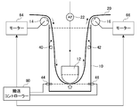
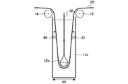
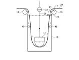
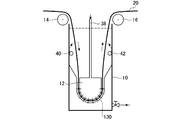
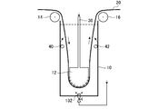
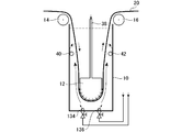
- the plating apparatus of the present embodiment is an apparatus that performs a plating process while transporting a resin film 20 such as a web-like polyimide film, and the direction perpendicular to the transport direction of the resin film 20.
- the so-called up-down conveyance system is adopted in which the film is continuously conveyed so as to be in the horizontal direction and takes a conveyance path that once descends and rises again inside the processing tank 10.
- bubbles that are generated in the plating solution and adhere to the surface of the resin film 20 by being shaken in the vertical direction instead of in the horizontal direction are formed in the plating solution.
- adverse effects due to bubbles can be minimized, and the occupation area of the entire production line can be reduced.
- the jet unit 12 is a member having a cylindrical shape on the bottom side and a rectangular shape on the upper side, and is formed by processing a resin such as PVC (polyvinyl chloride). Further, the jet unit 12 is provided in the width direction of the resin film 20 so as to have a dimension wider than the width of the resin film 20.
- the jet unit 12 is fixed to the processing tank 10 at the end in the width direction, but can also be detachable with respect to the processing tank 10, and can be moved in the processing tank 10 instead of being fixed. It is also possible to use a mechanism that is supported by being suspended from the upper part of the processing tank 10.
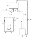
- a plating solution supply pipe 38 is connected to the jet unit 12, and the plating solution supplied through the plating solution supply pipe 38 is jetted from the jet unit 12 into the processing tank 10 with a predetermined liquid pressure.
- a jet unit 12 for conveying the resin film 20 in a non-contact manner is connected to the lower end of the plating solution supply pipe 38, but the head tank 18 is connected to the upper end of the plating solution supply pipe 38 more than the processing tank 10. It is arranged at a high position.
- the head tank 18 is a tank that temporarily stores the plating solution supplied by the pump 24 and supplies it to the jet unit 12, and pulsation of the plating solution resulting from the operation of the pump 24 is supplied to the jet unit 12. Can be suppressed.
- a series of mutation behaviors by this alkaline wet modification method is that when a polyimide resin is treated with an alkaline aqueous solution, a part of its surface is hydrolyzed and a part of the imide ring is cleaved, resulting in an amide group and a carboxyl group. Generate. This generated carboxyl group is easy to exchange cation ions, so that metal ions can be adsorbed.
- a conductive metal seed layer is formed on the surface of the resin film thus modified with a hydrophilic surface in advance by plating with a conductive metal such as Ni or an alloy thereof by an electroless plating method.
- the resin film 20 is fed by non-contact conveyance using the jet unit 12 using the plating apparatus according to the present embodiment.
- a conductive nickel seed layer having a thickness of about 10 to 300 nm may be formed on both surfaces, and Ni alloys such as Ni—P, Ni—B, and Ni—Cu may be used. Can be mentioned.
- the resin film wet processing apparatus of the present invention is arranged between the pretreatment process and the post-treatment process for forming the copper layer, and is premised on a continuous supply of a web-like resin film. If the problem such as film peeling does not occur, the resin film once wound after the pretreatment process can be supplied, and the resin film can be wound once before the posttreatment process.
- the conveyance can be stabilized.
- palladium on the plating deposition surface falls and the resin film 20 on the jet side.
- the plating film thickness on the surface becomes thin, and a difference in film thickness from the plating film thickness on the back surface of the resin film without jet discharge occurs, so that the front and back are not evenly plated. Therefore, in the plating apparatus of the present embodiment, the amount of ejection is limited, for example, the jet flow from the hole 15 of the jet unit 12 is 100 liters per minute, preferably 75 liters per minute, more preferably 50 liters per minute. Liters or less.
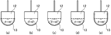
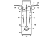
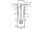
- the lower half of the jet unit 12 of the plating apparatus of this embodiment has a cylindrical shape, and is configured to discharge the plating solution from the center through holes 15 formed radially on the peripheral surface 13.
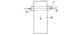
- the distribution of the holes 15 in the cross section obtained by cutting the jet unit 12 in the film transport direction determines the jet angle of the jet unit 12.
- the jet angle ⁇ of the jet unit 12 is 180 degrees
- the jet angle ⁇ of the jet unit 12 is 90 degrees
- the jet angle ⁇ of the jet unit 12 is 120 degrees.
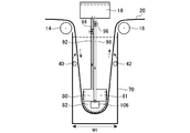
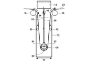
- the plating apparatus of the present embodiment shown in FIG. 10 has a treatment tank 70 having a relatively narrow span W1, and a jet unit 81 disposed therein includes a first chamber 80 disposed on the upper side of the unit. , And a second chamber 82 disposed below the unit.
- the first chamber 80 and the second chamber 82 are connected to the head tank 18 via independent plating solution supply pipes 92 and 96 without communicating with each other.
- the first chamber 80 is connected to the head tank 18 via a plating solution supply pipe 92 and a valve 94.
- the second chamber 82 is connected to the head tank 18 via a plating solution supply pipe 96 and a valve 98.
- the first chamber 80 has holes for ejecting the plating solution in the upper half of the jet unit 81, and the jet can be discharged from these holes in the horizontal direction.
- the second chamber 82 has a hole for ejecting the plating solution in the lower half of the jet unit 81, and can discharge the jet radially along the peripheral surface of the jet unit 81.
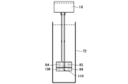
- the rudder member 108 controls the flow direction of the plating solution flowing into the second chamber 86 of the jet unit 85 from the end of the plating solution supply pipe 96 according to the direction of the rudder member 108. Therefore, when the resin film 20 is tilted, the tilt can be corrected by operating the rudder member 108.
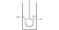
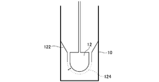
- U-shaped guide portions 120, 122, 124, and 126 are formed on the bottom side of the transport path as shown in FIGS.
- a U-shaped guide portion 120 shown in FIG. 21 has a U shape having a shape along the peripheral surface of the jet unit 12, and the jet unit inlet and outlet are formed by the upward flow of the liquid ejected from the jet unit. Is effectively prevented from disturbing the position of the film, so that reliable and stable film conveyance is performed.
- the U-shaped guide portion 122 shown in FIG. 22 has a hole 124 on the bottom side or has a mesh structure, and allows the liquid to enter and exit from the vicinity of the film and the outside of the guide 122 through the hole 124.
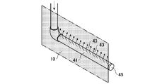
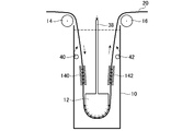
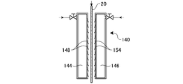
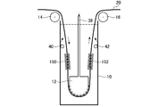
- the liquid flow of the outer unit of the side jet plates 140, 142, 150, 152 is made equal to the front and back, and the plating film thickness is made uniform. be able to. That is, since there is a jet from the jet unit 12 inside the film, the jet from the side jet plate is at least good.
- the side jet plate has been described as a type sandwiching the film, a side jet plate arranged only on one surface of the film may be provided.
- the conveyance state of the resin film may be monitored, and the side jet plate may be moved or the pressure of the plating solution output from the jet plate may be changed so as to perform stable film conveyance. .
Landscapes
- Chemical & Material Sciences (AREA)
- Engineering & Computer Science (AREA)
- Metallurgy (AREA)
- Chemical Kinetics & Catalysis (AREA)
- Materials Engineering (AREA)
- Mechanical Engineering (AREA)
- General Chemical & Material Sciences (AREA)
- Organic Chemistry (AREA)
- Manufacturing & Machinery (AREA)
- Microelectronics & Electronic Packaging (AREA)
- Inorganic Chemistry (AREA)
- Chemically Coating (AREA)
- Electroplating Methods And Accessories (AREA)
- Manufacturing Of Printed Wiring (AREA)
- Processing And Handling Of Plastics And Other Materials For Molding In General (AREA)
Abstract
Priority Applications (7)
| Application Number | Priority Date | Filing Date | Title |
|---|---|---|---|
| KR1020187019946A KR102516327B1 (ko) | 2016-01-12 | 2016-01-12 | 수지 필름의 습식 처리 장치 |
| JP2017561057A JP6626129B2 (ja) | 2016-01-12 | 2016-01-12 | 樹脂フィルムの湿式処理装置 |
| US16/068,996 US10640875B2 (en) | 2016-01-12 | 2016-01-12 | Wet type processing apparatus for resin film |
| PCT/JP2016/000126 WO2017122229A1 (fr) | 2016-01-12 | 2016-01-12 | Appareil de traitement de film de résine en voie humide |
| CN201680078470.7A CN108699696B (zh) | 2016-01-12 | 2016-01-12 | 树脂薄膜的湿式处理装置 |
| MYPI2018702423A MY193815A (en) | 2016-01-12 | 2016-01-12 | Wet type processing apparatus for resin film |
| TW105117753A TWI605153B (zh) | 2016-01-12 | 2016-06-04 | 樹脂薄膜的濕式處理裝置 |
Applications Claiming Priority (1)
| Application Number | Priority Date | Filing Date | Title |
|---|---|---|---|
| PCT/JP2016/000126 WO2017122229A1 (fr) | 2016-01-12 | 2016-01-12 | Appareil de traitement de film de résine en voie humide |
Publications (1)
| Publication Number | Publication Date |
|---|---|
| WO2017122229A1 true WO2017122229A1 (fr) | 2017-07-20 |
Family
ID=59312072
Family Applications (1)
| Application Number | Title | Priority Date | Filing Date |
|---|---|---|---|
| PCT/JP2016/000126 Ceased WO2017122229A1 (fr) | 2016-01-12 | 2016-01-12 | Appareil de traitement de film de résine en voie humide |
Country Status (7)
| Country | Link |
|---|---|
| US (1) | US10640875B2 (fr) |
| JP (1) | JP6626129B2 (fr) |
| KR (1) | KR102516327B1 (fr) |
| CN (1) | CN108699696B (fr) |
| MY (1) | MY193815A (fr) |
| TW (1) | TWI605153B (fr) |
| WO (1) | WO2017122229A1 (fr) |
Families Citing this family (3)
| Publication number | Priority date | Publication date | Assignee | Title |
|---|---|---|---|---|
| JP3220470U (ja) * | 2018-12-26 | 2019-03-07 | 株式会社Jcu | 樹脂フィルムの湿式処理装置 |
| CN111093323B (zh) * | 2019-12-12 | 2021-04-09 | 住井科技(深圳)有限公司 | 一种电路基板及其制备方法 |
| US11673158B1 (en) * | 2022-02-16 | 2023-06-13 | Jon Kyle Lavender | Method and apparatus for coating a drinking straw |
Citations (7)
| Publication number | Priority date | Publication date | Assignee | Title |
|---|---|---|---|---|
| JPS4858105U (fr) * | 1971-11-05 | 1973-07-24 | ||
| JPS59118653A (ja) * | 1982-12-25 | 1984-07-09 | Sumitomo Metal Ind Ltd | ストリツプの蛇行防止方法 |
| JP2003198097A (ja) * | 2001-12-28 | 2003-07-11 | Seiko Epson Corp | 配線基板の製造方法及び製造装置 |
| JP2008163407A (ja) * | 2006-12-28 | 2008-07-17 | Fujifilm Corp | めっき装置、液中ロール、およびフィルムのめっき方法 |
| JP2009099541A (ja) * | 2007-09-28 | 2009-05-07 | Fujifilm Corp | 導電性材料の製造方法及び導電性材料の製造装置 |
| JP2011174125A (ja) * | 2010-02-24 | 2011-09-08 | Panasonic Corp | 湿式処理装置 |
| JP2015048532A (ja) * | 2013-08-30 | 2015-03-16 | 佳冠電子股▲ふん▼有限公司 | フレキシブルプリント回路基板を製造するめっき設備 |
Family Cites Families (12)
| Publication number | Priority date | Publication date | Assignee | Title |
|---|---|---|---|---|
| LU53772A1 (fr) | 1967-05-30 | 1969-03-20 | ||
| JPS5513423Y2 (fr) * | 1974-12-18 | 1980-03-26 | ||
| US4269138A (en) * | 1979-04-23 | 1981-05-26 | Western Electric Company, Inc. | Apparatus for distributing liquid over a surface |
| US4349589A (en) * | 1979-04-23 | 1982-09-14 | Western Electric Co., Inc. | Method for distributing liquid over a surface |
| DE3903783A1 (de) * | 1989-02-09 | 1990-08-16 | Hauni Werke Koerber & Co Kg | Vorrichtung zum foerdern eines flachen gegenstandes |
| FI890785A7 (fi) * | 1989-02-17 | 1990-08-18 | Valmet Paper Machinery Inc | System av undertrycksmunstycken avsett foer behandling av roerliga aemnesbanor. |
| DE4033642A1 (de) * | 1990-10-23 | 1992-04-30 | Hoechst Ag | Leitvorrichtung zum fuehren, aus- und/oder umlenken einer materialbahn |
| JPH05320928A (ja) * | 1992-05-15 | 1993-12-07 | Hitachi Chem Co Ltd | 成形品の無電解めっき液及びめっき法 |
| JP4031586B2 (ja) * | 1999-02-25 | 2008-01-09 | Jfeスチール株式会社 | 帯状材の進行方向変更装置 |
| JP3805267B2 (ja) * | 2002-03-05 | 2006-08-02 | 富士写真フイルム株式会社 | 搬送方向転換装置 |
| JP4841996B2 (ja) * | 2006-03-31 | 2011-12-21 | 富士フイルム株式会社 | 洗浄装置、めっき被膜付きフィルムの製造装置、洗浄方法及びめっき被膜付きフィルムの製造方法 |
| JP5385625B2 (ja) | 2008-12-08 | 2014-01-08 | 株式会社Jcu | 2層フレキシブル銅張積層基材及びその製造方法 |
-
2016
- 2016-01-12 WO PCT/JP2016/000126 patent/WO2017122229A1/fr not_active Ceased
- 2016-01-12 CN CN201680078470.7A patent/CN108699696B/zh active Active
- 2016-01-12 KR KR1020187019946A patent/KR102516327B1/ko active Active
- 2016-01-12 MY MYPI2018702423A patent/MY193815A/en unknown
- 2016-01-12 US US16/068,996 patent/US10640875B2/en active Active
- 2016-01-12 JP JP2017561057A patent/JP6626129B2/ja active Active
- 2016-06-04 TW TW105117753A patent/TWI605153B/zh active
Patent Citations (7)
| Publication number | Priority date | Publication date | Assignee | Title |
|---|---|---|---|---|
| JPS4858105U (fr) * | 1971-11-05 | 1973-07-24 | ||
| JPS59118653A (ja) * | 1982-12-25 | 1984-07-09 | Sumitomo Metal Ind Ltd | ストリツプの蛇行防止方法 |
| JP2003198097A (ja) * | 2001-12-28 | 2003-07-11 | Seiko Epson Corp | 配線基板の製造方法及び製造装置 |
| JP2008163407A (ja) * | 2006-12-28 | 2008-07-17 | Fujifilm Corp | めっき装置、液中ロール、およびフィルムのめっき方法 |
| JP2009099541A (ja) * | 2007-09-28 | 2009-05-07 | Fujifilm Corp | 導電性材料の製造方法及び導電性材料の製造装置 |
| JP2011174125A (ja) * | 2010-02-24 | 2011-09-08 | Panasonic Corp | 湿式処理装置 |
| JP2015048532A (ja) * | 2013-08-30 | 2015-03-16 | 佳冠電子股▲ふん▼有限公司 | フレキシブルプリント回路基板を製造するめっき設備 |
Also Published As
| Publication number | Publication date |
|---|---|
| TW201725282A (zh) | 2017-07-16 |
| TWI605153B (zh) | 2017-11-11 |
| JPWO2017122229A1 (ja) | 2018-11-01 |
| MY193815A (en) | 2022-10-27 |
| CN108699696B (zh) | 2020-11-17 |
| US20190024238A1 (en) | 2019-01-24 |
| KR20180101391A (ko) | 2018-09-12 |
| KR102516327B1 (ko) | 2023-03-30 |
| JP6626129B2 (ja) | 2019-12-25 |
| CN108699696A (zh) | 2018-10-23 |
| US10640875B2 (en) | 2020-05-05 |
Similar Documents
| Publication | Publication Date | Title |
|---|---|---|
| JP6626129B2 (ja) | 樹脂フィルムの湿式処理装置 | |
| US8377252B2 (en) | Apparatus for spraying etchant onto printed circuit board | |
| JPWO2012176883A1 (ja) | 金属箔の製造方法及び製造装置 | |
| JPH0881799A (ja) | 電解めっき方法、電解めっき装置、電解めっき用ラック | |
| KR101403055B1 (ko) | 인쇄회로기판의 에칭방법 및 에칭장치 | |
| HK1260780B (en) | Resin film wet treatment apparatus | |
| HK1260780A1 (en) | Resin film wet treatment apparatus | |
| JP6465011B2 (ja) | 長尺フィルムの真空成膜装置 | |
| JP4424073B2 (ja) | エッチング装置および回路基板の製造方法 | |
| JP6972019B2 (ja) | 樹脂フィルム処理装置 | |
| KR20110067402A (ko) | 기판 도금 장치 | |
| CN207210538U (zh) | 卷对卷非接触式胶体金属化学镀设备 | |
| JP3062081B2 (ja) | 流体処理装置 | |
| JP6252401B2 (ja) | 成膜方法及びそれを用いた金属膜付樹脂フィルムの製造方法 | |
| JP3220470U (ja) | 樹脂フィルムの湿式処理装置 | |
| TWM536674U (zh) | 可撓性基板之水平連續式化學電鍍設備 | |
| TWI580817B (zh) | Flexible continuous chemical plating method and apparatus for flexible substrate | |
| JPH0575236A (ja) | 金属張り積層板のエツチング装置 | |
| CN1638603B (zh) | 在通过式处理设备中处理平坦物体的方法与装置 | |
| HK40023701B (en) | Wet processing device for resin film | |
| CN221621224U (zh) | 一种放线机构及焊线机 | |
| HK40010249A (en) | Resin film treatment device | |
| JP2016108573A (ja) | めっき処理装置及びめっき処理方法 | |
| JP4479226B2 (ja) | プリント配線板の製造装置 | |
| JP2017155286A (ja) | ロールツーロール処理装置及び処理方法 |
Legal Events
| Date | Code | Title | Description |
|---|---|---|---|
| 121 | Ep: the epo has been informed by wipo that ep was designated in this application |
Ref document number: 16884834 Country of ref document: EP Kind code of ref document: A1 |
|
| WWE | Wipo information: entry into national phase |
Ref document number: 2017561057 Country of ref document: JP |
|
| ENP | Entry into the national phase |
Ref document number: 20187019946 Country of ref document: KR Kind code of ref document: A |
|
| NENP | Non-entry into the national phase |
Ref country code: DE |
|
| 122 | Ep: pct application non-entry in european phase |
Ref document number: 16884834 Country of ref document: EP Kind code of ref document: A1 |