WO2017122579A1 - Circuit d'alimentation électrique à pont complet déphasé - Google Patents
Circuit d'alimentation électrique à pont complet déphasé Download PDFInfo
- Publication number
- WO2017122579A1 WO2017122579A1 PCT/JP2017/000190 JP2017000190W WO2017122579A1 WO 2017122579 A1 WO2017122579 A1 WO 2017122579A1 JP 2017000190 W JP2017000190 W JP 2017000190W WO 2017122579 A1 WO2017122579 A1 WO 2017122579A1
- Authority
- WO
- WIPO (PCT)
- Prior art keywords
- terminal
- circuit
- inductor
- switch element
- capacitor
- Prior art date
- Legal status (The legal status is an assumption and is not a legal conclusion. Google has not performed a legal analysis and makes no representation as to the accuracy of the status listed.)
- Ceased
Links
Images


Classifications
-
- H—ELECTRICITY
- H02—GENERATION; CONVERSION OR DISTRIBUTION OF ELECTRIC POWER
- H02M—APPARATUS FOR CONVERSION BETWEEN AC AND AC, BETWEEN AC AND DC, OR BETWEEN DC AND DC, AND FOR USE WITH MAINS OR SIMILAR POWER SUPPLY SYSTEMS; CONVERSION OF DC OR AC INPUT POWER INTO SURGE OUTPUT POWER; CONTROL OR REGULATION THEREOF
- H02M3/00—Conversion of DC power input into DC power output
- H02M3/22—Conversion of DC power input into DC power output with intermediate conversion into AC
- H02M3/24—Conversion of DC power input into DC power output with intermediate conversion into AC by static converters
- H02M3/28—Conversion of DC power input into DC power output with intermediate conversion into AC by static converters using discharge tubes with control electrode or semiconductor devices with control electrode to produce the intermediate AC
-
- H—ELECTRICITY
- H02—GENERATION; CONVERSION OR DISTRIBUTION OF ELECTRIC POWER
- H02M—APPARATUS FOR CONVERSION BETWEEN AC AND AC, BETWEEN AC AND DC, OR BETWEEN DC AND DC, AND FOR USE WITH MAINS OR SIMILAR POWER SUPPLY SYSTEMS; CONVERSION OF DC OR AC INPUT POWER INTO SURGE OUTPUT POWER; CONTROL OR REGULATION THEREOF
- H02M3/00—Conversion of DC power input into DC power output
- H02M3/22—Conversion of DC power input into DC power output with intermediate conversion into AC
- H02M3/24—Conversion of DC power input into DC power output with intermediate conversion into AC by static converters
- H02M3/28—Conversion of DC power input into DC power output with intermediate conversion into AC by static converters using discharge tubes with control electrode or semiconductor devices with control electrode to produce the intermediate AC
- H02M3/325—Conversion of DC power input into DC power output with intermediate conversion into AC by static converters using discharge tubes with control electrode or semiconductor devices with control electrode to produce the intermediate AC using devices of a triode or a transistor type requiring continuous application of a control signal
- H02M3/335—Conversion of DC power input into DC power output with intermediate conversion into AC by static converters using discharge tubes with control electrode or semiconductor devices with control electrode to produce the intermediate AC using devices of a triode or a transistor type requiring continuous application of a control signal using semiconductor devices only
Definitions
- the present invention relates to a phase shift type full bridge type power supply circuit.
- a return inductor has been added to the bridge circuit.
- Switching loss is suppressed.
- the switching loss of the switch element is suppressed by using the resonance characteristics of the LC resonance circuit composed of the return inductor and the capacitor of the bridge circuit (the parasitic capacitance of the switch element or the capacitor connected in parallel to the switch element). is doing.
- a phase shift type full bridge type power supply circuit capable of suppressing the loss of the transformer itself is known. See, for example, US Pat.
- the clamp diode can suppress the influence of the recovery surge voltage due to the return inductor to the rectifier diode of the rectifier circuit, but cannot suppress the recovery surge voltage due to the transformer leakage inductor. Since a transformer has a leakage inductor due to its structure, a recovery surge voltage is generated by the leakage inductor in the rectifier diode of the rectifier circuit. Therefore, conventionally, in order to suppress the recovery surge voltage, the rated voltage of the rectifier diode is increased in accordance with the recovery surge voltage. However, when the rated voltage of the rectifier diode is increased, the performance of the rectifier diode is degraded, and thus the recovery surge voltage is increased. In addition, the price of rectifier diodes will increase.
- An object according to one aspect of the present invention is to provide a phase shift type full bridge type power supply circuit that suppresses a recovery surge voltage due to a leakage inductor of a transformer.
- a phase shift type full bridge type power supply circuit includes a bridge circuit, a recovery surge protection circuit, a recovery surge suppression circuit, a transformer, and a rectifier circuit.
- the bridge circuit includes first to fourth switch elements connected in a full bridge type.
- the recovery surge protection circuit has first and second rectifying elements and is connected in parallel to the bridge circuit.
- one terminal of the inductor is connected to the anode terminal of the first rectifier element and the cathode terminal of the second rectifier element, and the other terminal of the inductor is one terminal of the third switch element.
- the fourth switch element is connected to one terminal of the fourth switch element, and a capacitor is connected in parallel to the inductor.
- the transformer has a primary winding and a secondary winding, and one terminal of the primary winding is connected to one terminal of the first switch element and one terminal of the second switch element. The other terminal of is connected to one terminal of the inductor.
- the rectifier circuit is connected to the secondary side of the transformer, and rectifies the AC voltage output from the transformer using the third and fourth rectifier elements.
- the control circuit controls driving and stopping of the first to fourth switch elements.
- the capacitor starts charging when the first and fourth switching elements are driven, and ends charging after the recovery of the fourth rectifying element, or the capacitor is driven when the second and third switching elements are driven. Charging is started, and charging ends after recovery of the third rectifying element occurs.
- FIG. 1 is a diagram showing an embodiment of a phase shift type full bridge type power supply circuit 1.
- the phase shift type full bridge type power supply circuit 1 includes a control circuit 2, an input capacitor C0, a bridge circuit, a recovery surge protection circuit 3 (clamp diode), a recovery surge suppression circuit 4, a transformer T, a rectifier circuit 5, and a smoothing circuit 6. ing.
- the phase shift type full bridge type power supply circuit 1 is, for example, a DC-DC converter that converts a DC input voltage Vin applied from a DC input power supply 7 into a DC output voltage Vout and drives a load 8.
- the control circuit 2 drives (ON: conduction) and stops (OFF: interruption) the switch elements Q1 to Q4 constituting the bridge circuit by control signals SQ1 to SQ4 output from a control terminal provided in the control circuit 2.
- the control circuit 2 includes, for example, a circuit configured using a CPU (Central Processing Unit), a multi-core CPU, a programmable device (FPGA (Field Programmable Gate Array), PLD (Programmable Logic Device), etc.), and a switching element Q1.
- CPU Central Processing Unit
- FPGA Field Programmable Gate Array
- PLD Programmable Logic Device
- the capacitor C0 is connected between the primary high voltage line HL1 connected to the positive terminal of the DC input power supply 7 and the primary low voltage line LL1 connected to the negative terminal of the DC input power supply 7.
- the bridge circuit has switch elements Q1 to Q4 (first to fourth switch elements) connected in a full bridge type.
- switch elements Q1 to Q4 MOSFETs (Metal / Oxide / Semiconductor / Field / Effect / Transistor), IGBTs (Insulated / Gate / Bipolor / Transistor), or the like may be used.
- MOSFETs Metal / Oxide / Semiconductor / Field / Effect / Transistor
- IGBTs Insulated / Gate / Bipolor / Transistor
- drain terminal (the other terminal) of the switch element Q1 and the drain terminal (the other terminal) of the switch element Q3 are connected, and the source terminal (the other terminal) of the switch element Q2 and the source terminal of the switch element Q4 (the other terminal) Terminal).
- capacitor C1 and the diode D1 are connected in parallel to the switch element Q1
- the capacitor C2 and the diode D2 are connected in parallel to the switch element Q2
- the capacitor C3 and the diode D3 are connected in parallel to the switch element Q3, and the switch element Q4
- a capacitor C4 and a diode D4 are connected in parallel.
- parasitic capacitors of the switch elements Q1 to Q4 may be used for the capacitors C1 to C4
- parasitic diodes of the switch elements Q1 to Q4 may be used for the diodes D1 to D4.
- gate terminals of the switch elements Q1 to Q4 are connected to the control terminal of the control circuit 2, and the switch elements Q1 to Q4 are controlled by the control signals SQ1 to SQ4 output from the control terminal.
- the recovery surge protection circuit 3 includes diodes D5 and D6 (first and second rectifying elements).
- the recovery surge protection circuit 3 is generated in the diodes D7 and D8 (third and fourth rectifier elements) of the rectifier circuit 5 connected to the secondary side of the transformer T by adding the inductor La (reflux inductor). Suppresses recovery surge voltage.
- the cathode terminal of the diode D5 is connected to the primary high-voltage line HL1, the drain terminal of the switch element Q1, and the drain terminal of the switch element Q3, the anode terminal of the diode D5 and the cathode terminal of the diode D6 are connected, and the anode of the diode D6
- the terminals are connected to the primary low-voltage line LL1, the source terminal of the switch element Q2, and the source terminal of the switch element Q4.
- one terminal of the inductor La is connected to the anode terminal of the diode D5 and the cathode terminal of the diode D6, and the other terminal of the inductor La is the source terminal of the switch element Q3 and the drain of the switch element Q4.
- the capacitor Ca is connected in parallel to the inductor La.
- the inductor La is an inductor provided to realize the ZVS of the switch elements Q1 to Q4, and configures an LC resonance circuit together with the capacitors C1 to C4 to use the resonance characteristics, thereby switching loss of the switch elements Q1 to Q4. Suppress.
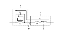
- the circuit in which the capacitor Ca is connected in parallel to the inductor La is a circuit that suppresses the recovery surge voltage generated in the diodes D7 and D8 of the rectifier circuit 5 connected to the secondary side of the transformer T by the leakage inductor L1 of the transformer T. It is. That is, the current I L flowing through the inductor La, and diode D7, current flows through the primary winding 9 of the transformer T to D8 recovery upon occurrence of I T (load current + recovery current), a by causing charged in the capacitor Ca, trans
- This circuit reduces the input voltage (2 ⁇ Vin / N) applied to the secondary windings 10a and 10b of T and suppresses the recovery surge voltage generated by the leakage inductor L1 of the transformer T.
- N is a turn ratio of the primary winding 9 and the secondary windings 10a and 10b of the transformer T, and is N: 1: 1.
- the transformer T has a primary winding 9 and secondary windings 10a and 10b.
- One terminal of the primary winding 9 is connected to the source terminal of the switch element Q1 and the drain terminal of the switch element Q2, and the other terminal of the primary winding 9 is connected to one terminal of the inductor La.
- One terminal of each of the secondary windings 10a and 10b is connected to each other at a midpoint (center tap).
- the rectifier circuit 5 is connected to the secondary side of the transformer T, and rectifies and outputs the AC voltage output from the transformer T using the diodes D7 and D8.
- the other terminal of the secondary winding 10a is connected to the cathode terminal of the diode D7
- the other terminal of the secondary winding 10b is connected to the cathode terminal of the diode D8, and the middle point is one of the inductors L0 of the smoothing circuit 6.
- the anode terminals of the diodes D7 and D8 are connected to the secondary low voltage line LL2.
- the diodes D7 and D8 may be MOSFETs. However, when a MOSFET is used, it is preferable to drive the MOSFET itself in synchronization with a period during which the parasitic diode of the MOSFET is conductive.
- the smoothing circuit 6 has an inductor L0 and a capacitor C5.
- the smoothing circuit 6 smoothes the voltage rectified by the rectifying circuit 5 and outputs a DC output voltage Vout.
- power is supplied to the load 8.
- the other terminal of the inductor L0 is connected to one terminal of the capacitor C5 and the secondary high voltage line HL2, and the other terminal of the capacitor C5 is connected to the secondary low voltage line LL2.
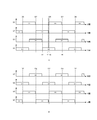
- FIG. 2A is a diagram showing the switching timing (driving (on) and stopping) when the switching elements Q1 and Q2 are in the leading phase.
- FIG. 3 is a diagram showing a current flow of the recovery surge suppression circuit 4.
- the recovery surge voltage of the diode D8 has a form in which the resonance voltage due to the parasitic capacitance of the leakage inductor L1 and the diode D8 is superimposed around the voltage 2 ⁇ Vin / N applied to the secondary windings 10a and 10b of the transformer T. . Therefore, when there is no capacitor Ca as in the conventional phase shift type full bridge type power supply circuit, a recovery surge voltage exceeding the rated voltage of the diode D8 is applied as shown in FIGS.
- FIG. 4 is a diagram illustrating a waveform when a recovery surge of the diode D8 of the rectifier circuit 5 occurs.
- the voltage V T2 of the secondary windings 10a and 10b of the transformer T is 2 ⁇ Vin even if the switch elements Q1 and Q4 are driven at the time ta shown in FIGS. Not lower than / N. Therefore, when the recovery surge occurrence time t1 of the diode D8 is reached, the recovery surge voltage is superimposed around the voltage 2 ⁇ Vin / N and exceeds the rated voltage of the diode D8.
- the capacitor Ca starts charging when the switch elements Q1 and Q4 are driven and the recovery surge voltage of the diode D8 is terminated after the recovery surge is generated, thereby suppressing the recovery surge voltage.
- the elements Q2 and Q3 are driven. That is, when the switch elements Q2 and Q3 are driven at t4 in FIG. 2, the capacitor Ca can suppress the recovery surge voltage by starting charging and ending charging after the recovery surge of the diode D7 occurs. .
- the capacitor Ca starts charging, the voltage at the measurement point TP in FIG. 1 approaches 0 [V] from the DC input voltage Vin, contrary to E in FIG.
- FIG. 2 is a diagram illustrating switching timing (driving (on) and stopping) when the switching elements Q1 and Q2 are in a delayed phase.
- the rated voltage of the diodes D7 and D8 can be lowered by suppressing the recovery surge voltage, the forward voltage (on-time voltage drop) can be reduced and the loss can be reduced. In addition, the prices of the diodes D7 and D8 are reduced.
Landscapes
- Engineering & Computer Science (AREA)
- Power Engineering (AREA)
- Dc-Dc Converters (AREA)
Abstract
La présente invention concerne un circuit d'alimentation électrique à pont complet déphasé qui est équipé : d'un circuit à pont ; d'un circuit de protection contre les surtensions de récupération (3) connecté en parallèle au circuit à pont ; d'un circuit de suppression de surtension de récupération (4), une borne d'un inducteur (La) étant connectée à l'anode d'un premier élément de redressement (D5) et la cathode d'un deuxième de redressement (D6), et l'autre borne de l'inducteur à une borne d'un troisième élément commutateur (Q3) et une borne d'un quatrième élément commutateur (Q4), et un condensateur (Ca) étant connecté en parallèle à l'inducteur ; et d'un circuit de redressement (5) qui possède un troisième élément de redressement (D7) et un quatrième élément de redressement (D8). Le condensateur est chargé lorsqu'un premier élément commutateur (Q1) et le quatrième élément commutateur (Q4) sont excités, et la charge se termine après qu'une surtension de récupération du quatrième élément de redressement est générée ; ou, le condensateur est chargé lorsque le deuxième élément commutateur (Q2) et le troisième élément commutateur (Q3) sont excités, et la charge se termine après qu'une surtension de récupération du troisième élément de redressement est générée.
Applications Claiming Priority (2)
| Application Number | Priority Date | Filing Date | Title |
|---|---|---|---|
| JP2016-003374 | 2016-01-12 | ||
| JP2016003374A JP6485366B2 (ja) | 2016-01-12 | 2016-01-12 | 位相シフト方式フルブリッジ型電源回路 |
Publications (1)
| Publication Number | Publication Date |
|---|---|
| WO2017122579A1 true WO2017122579A1 (fr) | 2017-07-20 |
Family
ID=59312047
Family Applications (1)
| Application Number | Title | Priority Date | Filing Date |
|---|---|---|---|
| PCT/JP2017/000190 Ceased WO2017122579A1 (fr) | 2016-01-12 | 2017-01-06 | Circuit d'alimentation électrique à pont complet déphasé |
Country Status (2)
| Country | Link |
|---|---|
| JP (1) | JP6485366B2 (fr) |
| WO (1) | WO2017122579A1 (fr) |
Families Citing this family (2)
| Publication number | Priority date | Publication date | Assignee | Title |
|---|---|---|---|---|
| US11239745B2 (en) * | 2018-04-11 | 2022-02-01 | Aerojet Rocketdyne, Inc | Power converter including a recirculating snubber |
| JP7230738B2 (ja) | 2019-08-09 | 2023-03-01 | 株式会社オートネットワーク技術研究所 | 複合部品 |
Citations (3)
| Publication number | Priority date | Publication date | Assignee | Title |
|---|---|---|---|---|
| WO2007000830A1 (fr) * | 2005-06-29 | 2007-01-04 | Murata Manufacturing Co., Ltd. | Convertisseur cc-cc |
| JP2008187801A (ja) * | 2007-01-29 | 2008-08-14 | Tdk Corp | スイッチング電源装置 |
| WO2015118631A1 (fr) * | 2014-02-05 | 2015-08-13 | 三菱電機株式会社 | Chargeur véhiculaire et procédé de suppression des surtensions d'un chargeur embarqué véhiculaire |
-
2016
- 2016-01-12 JP JP2016003374A patent/JP6485366B2/ja active Active
-
2017
- 2017-01-06 WO PCT/JP2017/000190 patent/WO2017122579A1/fr not_active Ceased
Patent Citations (3)
| Publication number | Priority date | Publication date | Assignee | Title |
|---|---|---|---|---|
| WO2007000830A1 (fr) * | 2005-06-29 | 2007-01-04 | Murata Manufacturing Co., Ltd. | Convertisseur cc-cc |
| JP2008187801A (ja) * | 2007-01-29 | 2008-08-14 | Tdk Corp | スイッチング電源装置 |
| WO2015118631A1 (fr) * | 2014-02-05 | 2015-08-13 | 三菱電機株式会社 | Chargeur véhiculaire et procédé de suppression des surtensions d'un chargeur embarqué véhiculaire |
Also Published As
| Publication number | Publication date |
|---|---|
| JP6485366B2 (ja) | 2019-03-20 |
| JP2017127051A (ja) | 2017-07-20 |
Similar Documents
| Publication | Publication Date | Title |
|---|---|---|
| US9190911B2 (en) | Auxiliary resonant apparatus for LLC converters | |
| US9124190B2 (en) | Isolated switched mode power supply | |
| US9350260B2 (en) | Startup method and system for resonant converters | |
| US20150124487A1 (en) | Adjustable Resonant Apparatus for Power Converters | |
| JP6241334B2 (ja) | 電流共振型dcdcコンバータ | |
| CN105684287A (zh) | 用于谐振转换器的栅驱动装置 | |
| JP5644125B2 (ja) | 直流−直流変換回路の起動方法 | |
| US8064228B2 (en) | Power supply apparatus with current-sharing function | |
| JP2014143911A (ja) | コンバーター | |
| US9564819B2 (en) | Switching power supply circuit | |
| US6999325B2 (en) | Current/voltage converter arrangement | |
| JP2015042080A (ja) | スイッチング電源装置 | |
| US9748851B2 (en) | Switching power supply apparatus with snubber circuit | |
| JP4410599B2 (ja) | スイッチング電源装置 | |
| US9263959B2 (en) | Forward converter with self-driven BJT synchronous rectifier | |
| JP4110477B2 (ja) | Dc−dcコンバータ | |
| KR20160101808A (ko) | 풀브리지 dc-dc 컨버터 | |
| JP5516055B2 (ja) | 電力変換装置 | |
| KR20150070898A (ko) | 직류-직류 컨버터 및 이의 스위칭 방법 | |
| JP6458235B2 (ja) | スイッチング電源装置 | |
| JP6485366B2 (ja) | 位相シフト方式フルブリッジ型電源回路 | |
| US11356029B2 (en) | Rectifying circuit and switched-mode power supply incorporating rectifying circuit | |
| JP6129687B2 (ja) | スイッチング電源装置 | |
| JPH1118426A (ja) | スイッチング電源回路 | |
| JP2006191706A (ja) | 直流変換装置 |
Legal Events
| Date | Code | Title | Description |
|---|---|---|---|
| 121 | Ep: the epo has been informed by wipo that ep was designated in this application |
Ref document number: 17738334 Country of ref document: EP Kind code of ref document: A1 |
|
| NENP | Non-entry into the national phase |
Ref country code: DE |
|
| 122 | Ep: pct application non-entry in european phase |
Ref document number: 17738334 Country of ref document: EP Kind code of ref document: A1 |