WO2017126325A1 - Feuille de câblage étirable et feuille de capteur tactile étirable - Google Patents
Feuille de câblage étirable et feuille de capteur tactile étirable Download PDFInfo
- Publication number
- WO2017126325A1 WO2017126325A1 PCT/JP2017/000133 JP2017000133W WO2017126325A1 WO 2017126325 A1 WO2017126325 A1 WO 2017126325A1 JP 2017000133 W JP2017000133 W JP 2017000133W WO 2017126325 A1 WO2017126325 A1 WO 2017126325A1
- Authority
- WO
- WIPO (PCT)
- Prior art keywords
- sheet
- stretchable
- elastomer sheet
- elastomer
- shape
- Prior art date
- Legal status (The legal status is an assumption and is not a legal conclusion. Google has not performed a legal analysis and makes no representation as to the accuracy of the status listed.)
- Ceased
Links
Images

Classifications
-
- B—PERFORMING OPERATIONS; TRANSPORTING
- B32—LAYERED PRODUCTS
- B32B—LAYERED PRODUCTS, i.e. PRODUCTS BUILT-UP OF STRATA OF FLAT OR NON-FLAT, e.g. CELLULAR OR HONEYCOMB, FORM
- B32B5/00—Layered products characterised by the non- homogeneity or physical structure, i.e. comprising a fibrous, filamentary, particulate or foam layer; Layered products characterised by having a layer differing constitutionally or physically in different parts
- B32B5/22—Layered products characterised by the non- homogeneity or physical structure, i.e. comprising a fibrous, filamentary, particulate or foam layer; Layered products characterised by having a layer differing constitutionally or physically in different parts characterised by the presence of two or more layers which are next to each other and are fibrous, filamentary, formed of particles or foamed
- B32B5/24—Layered products characterised by the non- homogeneity or physical structure, i.e. comprising a fibrous, filamentary, particulate or foam layer; Layered products characterised by having a layer differing constitutionally or physically in different parts characterised by the presence of two or more layers which are next to each other and are fibrous, filamentary, formed of particles or foamed one layer being a fibrous or filamentary layer
-
- H—ELECTRICITY
- H05—ELECTRIC TECHNIQUES NOT OTHERWISE PROVIDED FOR
- H05K—PRINTED CIRCUITS; CASINGS OR CONSTRUCTIONAL DETAILS OF ELECTRIC APPARATUS; MANUFACTURE OF ASSEMBLAGES OF ELECTRICAL COMPONENTS
- H05K1/00—Printed circuits
- H05K1/02—Details
- H05K1/0277—Bendability or stretchability details
- H05K1/0283—Stretchable printed circuits
-
- B—PERFORMING OPERATIONS; TRANSPORTING
- B32—LAYERED PRODUCTS
- B32B—LAYERED PRODUCTS, i.e. PRODUCTS BUILT-UP OF STRATA OF FLAT OR NON-FLAT, e.g. CELLULAR OR HONEYCOMB, FORM
- B32B25/00—Layered products comprising a layer of natural or synthetic rubber
- B32B25/10—Layered products comprising a layer of natural or synthetic rubber next to a fibrous or filamentary layer
-
- B—PERFORMING OPERATIONS; TRANSPORTING
- B32—LAYERED PRODUCTS
- B32B—LAYERED PRODUCTS, i.e. PRODUCTS BUILT-UP OF STRATA OF FLAT OR NON-FLAT, e.g. CELLULAR OR HONEYCOMB, FORM
- B32B7/00—Layered products characterised by the relation between layers; Layered products characterised by the relative orientation of features between layers, or by the relative values of a measurable parameter between layers, i.e. products comprising layers having different physical, chemical or physicochemical properties; Layered products characterised by the interconnection of layers
- B32B7/02—Physical, chemical or physicochemical properties
- B32B7/022—Mechanical properties
-
- G—PHYSICS
- G06—COMPUTING OR CALCULATING; COUNTING
- G06F—ELECTRIC DIGITAL DATA PROCESSING
- G06F3/00—Input arrangements for transferring data to be processed into a form capable of being handled by the computer; Output arrangements for transferring data from processing unit to output unit, e.g. interface arrangements
- G06F3/01—Input arrangements or combined input and output arrangements for interaction between user and computer
- G06F3/03—Arrangements for converting the position or the displacement of a member into a coded form
- G06F3/041—Digitisers, e.g. for touch screens or touch pads, characterised by the transducing means
-
- G—PHYSICS
- G06—COMPUTING OR CALCULATING; COUNTING
- G06F—ELECTRIC DIGITAL DATA PROCESSING
- G06F3/00—Input arrangements for transferring data to be processed into a form capable of being handled by the computer; Output arrangements for transferring data from processing unit to output unit, e.g. interface arrangements
- G06F3/01—Input arrangements or combined input and output arrangements for interaction between user and computer
- G06F3/03—Arrangements for converting the position or the displacement of a member into a coded form
- G06F3/041—Digitisers, e.g. for touch screens or touch pads, characterised by the transducing means
- G06F3/0416—Control or interface arrangements specially adapted for digitisers
- G06F3/04164—Connections between sensors and controllers, e.g. routing lines between electrodes and connection pads
-
- G—PHYSICS
- G06—COMPUTING OR CALCULATING; COUNTING
- G06F—ELECTRIC DIGITAL DATA PROCESSING
- G06F3/00—Input arrangements for transferring data to be processed into a form capable of being handled by the computer; Output arrangements for transferring data from processing unit to output unit, e.g. interface arrangements
- G06F3/01—Input arrangements or combined input and output arrangements for interaction between user and computer
- G06F3/03—Arrangements for converting the position or the displacement of a member into a coded form
- G06F3/041—Digitisers, e.g. for touch screens or touch pads, characterised by the transducing means
- G06F3/044—Digitisers, e.g. for touch screens or touch pads, characterised by the transducing means by capacitive means
- G06F3/0446—Digitisers, e.g. for touch screens or touch pads, characterised by the transducing means by capacitive means using a grid-like structure of electrodes in at least two directions, e.g. using row and column electrodes
-
- H—ELECTRICITY
- H01—ELECTRIC ELEMENTS
- H01B—CABLES; CONDUCTORS; INSULATORS; SELECTION OF MATERIALS FOR THEIR CONDUCTIVE, INSULATING OR DIELECTRIC PROPERTIES
- H01B7/00—Insulated conductors or cables characterised by their form
- H01B7/04—Flexible cables, conductors, or cords, e.g. trailing cables
-
- H—ELECTRICITY
- H05—ELECTRIC TECHNIQUES NOT OTHERWISE PROVIDED FOR
- H05K—PRINTED CIRCUITS; CASINGS OR CONSTRUCTIONAL DETAILS OF ELECTRIC APPARATUS; MANUFACTURE OF ASSEMBLAGES OF ELECTRICAL COMPONENTS
- H05K3/00—Apparatus or processes for manufacturing printed circuits
- H05K3/10—Apparatus or processes for manufacturing printed circuits in which conductive material is applied to the insulating support in such a manner as to form the desired conductive pattern
- H05K3/103—Apparatus or processes for manufacturing printed circuits in which conductive material is applied to the insulating support in such a manner as to form the desired conductive pattern by bonding or embedding conductive wires or strips
-
- B—PERFORMING OPERATIONS; TRANSPORTING
- B32—LAYERED PRODUCTS
- B32B—LAYERED PRODUCTS, i.e. PRODUCTS BUILT-UP OF STRATA OF FLAT OR NON-FLAT, e.g. CELLULAR OR HONEYCOMB, FORM
- B32B2457/00—Electrical equipment
- B32B2457/20—Displays, e.g. liquid crystal displays, plasma displays
- B32B2457/208—Touch screens
-
- G—PHYSICS
- G06—COMPUTING OR CALCULATING; COUNTING
- G06F—ELECTRIC DIGITAL DATA PROCESSING
- G06F2203/00—Indexing scheme relating to G06F3/00 - G06F3/048
- G06F2203/041—Indexing scheme relating to G06F3/041 - G06F3/045
- G06F2203/04102—Flexible digitiser, i.e. constructional details for allowing the whole digitising part of a device to be flexed or rolled like a sheet of paper
-
- H—ELECTRICITY
- H05—ELECTRIC TECHNIQUES NOT OTHERWISE PROVIDED FOR
- H05K—PRINTED CIRCUITS; CASINGS OR CONSTRUCTIONAL DETAILS OF ELECTRIC APPARATUS; MANUFACTURE OF ASSEMBLAGES OF ELECTRICAL COMPONENTS
- H05K2201/00—Indexing scheme relating to printed circuits covered by H05K1/00
- H05K2201/01—Dielectrics
- H05K2201/0104—Properties and characteristics in general
- H05K2201/0133—Elastomeric or compliant polymer
-
- H—ELECTRICITY
- H05—ELECTRIC TECHNIQUES NOT OTHERWISE PROVIDED FOR
- H05K—PRINTED CIRCUITS; CASINGS OR CONSTRUCTIONAL DETAILS OF ELECTRIC APPARATUS; MANUFACTURE OF ASSEMBLAGES OF ELECTRICAL COMPONENTS
- H05K2201/00—Indexing scheme relating to printed circuits covered by H05K1/00
- H05K2201/10—Details of components or other objects attached to or integrated in a printed circuit board
- H05K2201/10007—Types of components
- H05K2201/10151—Sensor
-
- H—ELECTRICITY
- H05—ELECTRIC TECHNIQUES NOT OTHERWISE PROVIDED FOR
- H05K—PRINTED CIRCUITS; CASINGS OR CONSTRUCTIONAL DETAILS OF ELECTRIC APPARATUS; MANUFACTURE OF ASSEMBLAGES OF ELECTRICAL COMPONENTS
- H05K2201/00—Indexing scheme relating to printed circuits covered by H05K1/00
- H05K2201/10—Details of components or other objects attached to or integrated in a printed circuit board
- H05K2201/10227—Other objects, e.g. metallic pieces
- H05K2201/10287—Metal wires as connectors or conductors
-
- H—ELECTRICITY
- H05—ELECTRIC TECHNIQUES NOT OTHERWISE PROVIDED FOR
- H05K—PRINTED CIRCUITS; CASINGS OR CONSTRUCTIONAL DETAILS OF ELECTRIC APPARATUS; MANUFACTURE OF ASSEMBLAGES OF ELECTRICAL COMPONENTS
- H05K2203/00—Indexing scheme relating to apparatus or processes for manufacturing printed circuits covered by H05K3/00
- H05K2203/01—Tools for processing; Objects used during processing
- H05K2203/0104—Tools for processing; Objects used during processing for patterning or coating
- H05K2203/0143—Using a roller; Specific shape thereof; Providing locally adhesive portions thereon
-
- H—ELECTRICITY
- H05—ELECTRIC TECHNIQUES NOT OTHERWISE PROVIDED FOR
- H05K—PRINTED CIRCUITS; CASINGS OR CONSTRUCTIONAL DETAILS OF ELECTRIC APPARATUS; MANUFACTURE OF ASSEMBLAGES OF ELECTRICAL COMPONENTS
- H05K3/00—Apparatus or processes for manufacturing printed circuits
- H05K3/0011—Working of insulating substrates or insulating layers
- H05K3/0014—Shaping of the substrate, e.g. by moulding
Definitions
- the present invention relates to a stretchable wiring sheet and a stretchable touch sensor sheet excellent in stretchability, in which a conductive wire is sandwiched between two stretchable elastomer sheets.
- Stretchable wiring sheets for example, antennas and wiring for RFID devices that require flexibility, wiring for motion analysis sensors in sports science, clothes-type heart rate / electrocardiogram monitors, wiring sheets for robot movable parts, and commands to computers
- touch sensor sheets for bending sensors and wiring sheets for bending sensors to be mounted on fingers, elbow joints, and knee joints for remote control of a robot.
- Such a stretchable wiring sheet is required to have excellent stretchability and a small change in resistance value due to stretching.
- the present invention solves the above-mentioned problems in the prior art, can be produced easily and at low cost, has high flexibility and durability, and has a high stretchable wiring sheet having a small resistance value change due to stretching and It is an object to provide an elastic touch sensor sheet.
- the cross-sectional shape of the cross section is circular or elliptical between the elastic first elastomer sheet and the elastic second elastomer sheet bonded to the first elastomer sheet.
- the conductive wire plastically deformed into a wave shape that is periodically curved along the longitudinal direction, and the height direction of the wave shape wave is the first elastomer sheet and
- the stretchable wiring sheet is sandwiched in a state along the in-plane direction of the opposing surface of the second elastomer sheet.
- the conductive wire includes a metal structure composed of crystal grains having an elongated shape in a longitudinal section.
- ⁇ 3> The stretchable wiring sheet according to any one of ⁇ 1> to ⁇ 2>, wherein the lead wire has a diameter of 50 ⁇ m at most.
- ⁇ 4> The stretchable wiring sheet according to any one of ⁇ 1> to ⁇ 3>, wherein the Young's modulus of the conductive wire is at least 150 GPa.
- ⁇ 5> The stretchable wiring sheet according to any one of ⁇ 1> to ⁇ 4>, wherein the wave height in the wave shape is 20 ⁇ m to 5 mm.
- the ratio of A / B is 0.05 to 0.5.
- the stretchable wiring sheet according to any one of ⁇ 1> to ⁇ 5>.
- the cross-sectional shape of the cross section is circular or elliptical.
- the conductive wire plastically deformed into a wave shape that is periodically curved along the longitudinal direction, and the height direction of the wave shape wave is the first elastomer sheet and Arranged in a state along the in-plane direction of the opposing surface of the second elastomer sheet, the first elastomer sheet and the second elastomer sheet are formed of a transparent material, and a plurality of the conductive wires are arranged in parallel.
- the above-mentioned problems in the prior art can be solved, and can be manufactured easily and at low cost, and is highly flexible and durable, and has a high elasticity that has a small resistance change due to expansion and contraction.
- a wiring sheet and a stretchable touch sensor sheet can be provided.
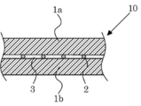
- FIGS. 1 (a) and 1 (b) A stretchable wiring sheet 10 according to an embodiment of the present invention will be described with reference to FIGS. 1 (a) and 1 (b).
- 1A is an explanatory view showing the sheet upper surface of the stretchable wiring sheet
- FIG. 1B is a sectional view showing a sheet cross section of the stretchable sheet.
- a stretchable wiring sheet 10 is composed of a stretchable first elastomer sheet 1a and a stretchable second adhesive bonded to the first elastomer sheet 1a. Elastomer sheet 1b and a conductor 2 sandwiched between the first elastomer sheet 1a and the second elastomer sheet 1b.
- the first elastomer sheet 1a and the second elastomer sheet 1b are not particularly limited as long as they elastically deform and expand and contract, and can be appropriately selected according to the purpose, and are formed of a known elastomer material.
- a sheet can be used, and examples thereof include natural rubber, diene rubber, non-diene rubber, urethane elastomer, styrene elastomer, and silicon elastomer.
- the elastomer sheet 1a and the second elastomer sheet 1b are required to have transparency.
- a sheet formed of a known transparent elastomer material can be used as the first elastomer sheet 1a and the second elastomer sheet 1b.
- a known urethane elastomer sheet or acrylic elastomer is used as the first elastomer sheet 1a and the second elastomer sheet 1b.
- a sheet or a silicon-based elastomer sheet can be used.
- the term “transparency” indicates that the visible light transmittance is 50% or more.
- the stretchable wiring sheet 10 can be made highly stretchable, so that it is large, 50% (natural length 1.5 times or more), more preferably 300% (4 times the natural length) or more, and particularly preferably 500% (6 times the natural length) or more.
- limit elongation ratio indicates an elongation ratio at which breakage occurs when the sheet is stretched.
- the lower limit of the thickness of the first elastomer sheet 1a and the second elastomer sheet 1b is not particularly limited and depends on the forming material, but is preferably 5 ⁇ m. When the thickness is less than 5 ⁇ m, the shape of the corrugated wire appears clearly on the film surface and may be easily recognized. Moreover, there is no restriction
- the pressure-sensitive adhesive layer 3 is formed on at least one facing surface of these sheets and these sheets are bonded together.
- the pressure-sensitive adhesive layer 3 is suitably used so that physical properties such as flexibility and stretchability after curing do not hinder the physical properties such as flexibility and stretchability of the first elastomer sheet 1a and the second elastomer sheet 1b.
- the material to be selected include a known rubber-based adhesive, urethane-based adhesive, acrylic-based adhesive, and silicon-based adhesive.
- the adhesive strength of the adhesive layer 3 is not particularly limited, but is preferably at least 0.5 N / cm to 10 N / cm. If the adhesive strength is less than 0.5 N / cm, the elastomer sheet and the conductive wire 2 may be peeled off during expansion and contraction, and transparency may be lost. If it exceeds 10 N / cm, the load on the wiring during expansion and contraction increases. There is a risk of disconnection.
- the cross-sectional shape of the conducting wire 2 is a circular shape, an elliptical shape, or a track shape, and the circular shape is optimal among them.
- stress concentration occurs in the angular treatment part, and in contrast to the rectangular cross-section of the conductive wire, the conductor 2 has a curved corner, so an external force is applied in the bending direction. At this time, stress concentration is less likely to occur, and the risk of disconnection can be reduced. Therefore, the durability which was excellent in the stretchable wiring sheet 10 can be provided by using such a conducting wire 2.
- a cross section means the surface cut
- the conducting wire 2 is plastically deformed into a wave shape that is periodically curved along the longitudinal direction, and the wave height direction of the wave shape is the first elastomer sheet 1a and the second elastomer sheet. It is clamped between both sheets in a state along the in-plane direction of the facing surface of 1b.
- the conducting wire 2 By arranging the conducting wire 2 between the first elastomer sheet 1a and the second elastomer sheet 1b in such a state, the highly flexible stretchable wiring sheet 10 having high flexibility is formed. That is, by using the linear conductive wire 2 without using a circuit board with poor flexibility, the conductive wire 2 can easily follow the shape changes of the first elastomer sheet 1a and the second elastomer sheet 1b.
- the stretchable wiring sheet 10 is provided with excellent flexibility and stretchability. Moreover, in this conducting wire 2, the length of the path
- unloading indicates a state in which the elastic wiring sheet 10 is not subjected to a shape change such as stretching or bending.
- a wire diameter of the conducting wire 2 is 50 micrometers at most, it is more preferable that it is 25 micrometers, and it is 12 micrometers. Particularly preferred.
- the wire diameter in case the cross-sectional shape of the conducting wire 2 is other than circular shape the diameter in the position where length becomes the longest in the cross-sectional shape corresponds. Further, the lower limit of the wire diameter of the conducting wire 2 is about 1 ⁇ m.
- the conducting wire 2 is not particularly limited, but preferably includes a metal structure composed of crystal grains that are elongated in a longitudinal section.
- a metal structure composed of crystal grains that are elongated in a longitudinal section.
- the strength and fatigue resistance of the conductive wire 2 itself are improved, and as a result, the durability of the stretchable wiring sheet 10 can be further improved.
- limiting in particular as a formation method of such conducting wire 2 The formation method by plastic processing, such as a well-known wire drawing processing and rolling processing, can be mentioned, Depending on the condition of the said plastic working, the conducting wire 2 Even when the forming material is copper, the tensile strength can be about 400 MPa.
- the wire diameter of the conducting wire 2 is set to be extremely thin as described above. Therefore, it is necessary to select the material and set the wavy shape so that the conductive wire 2 does not break when a shape change such as stretching or bending is applied to the stretchable wiring sheet 10.
- the Young's modulus (longitudinal elastic modulus) of the conducting wire 2 is preferably at least 150 GPa from the viewpoint of improving the flexibility and durability of the conducting wire 2.
- the upper limit of the Young's modulus (longitudinal elastic modulus) is about 500 GPa.
- the Young's modulus (longitudinal elastic modulus) can be calculated by conducting a tensile test on the conducting wire 2, obtaining a stress-strain diagram, and determining the slope of the straight line portion in the stress-strain diagram.
- the A / B ratio is not particularly limited, but 0 .05 to 0.5 is preferable. That is, if the A / B ratio is less than 0.05, distortion at the curved portion may increase and disconnection may occur, and if it exceeds 0.5, it is difficult to form a periodic wave shape. Sometimes.
- a / D The ratio is 3 to 100, more preferably 5 to 30, so that stress concentration hardly occurs even when an external force is applied in the bending direction, and the risk of disconnection can be reduced. That is, if the A / D ratio is less than 3, the risk of breakage increases due to an increase in bending stress. Sometimes.
- the wave height in the wavy shape is not particularly limited, but is preferably 20 ⁇ m to 5 mm. That is, if the wave height is less than 20 ⁇ m, the conductor 2 may be substantially rod-shaped, and the extension range of the stretchable wiring sheet 10 may be narrowed. If it exceeds 5 mm, the conductor 2 in the stretchable wiring sheet 10 is visually recognized. It becomes easy and the necessary transparency may not be obtained.
- the wavy waveform can be confirmed from the outside of the stretchable wiring sheet 10 using a known optical microscope, digital microscope, electron microscope, or X-ray microscope.
- the resistivity of the conductor 2 is not particularly limited and may be appropriately selected depending on the intended purpose.
- the resistivity is about 1.0 ⁇ 10 ⁇ 6 ⁇ ⁇ cm to 1.0 ⁇ 10 ⁇ 3 ⁇ ⁇ cm.
- the material for forming the conductive wire 2 is not particularly limited and can be appropriately selected in consideration of the above characteristics.
- a well-known metal wire, carbon fiber, etc. are mentioned.
- the metal wire about the thing with comparatively high resistivity like the said piano wire and the said SUS304 wire, the metal with low resistivity, such as copper and silver, can also be plated and used.
- one conductor 2 is arranged, but a plurality of conductors 2 can be arranged in parallel.
- the stretchable wiring sheet 10 configured as described above is flexible and durable, and has a small change in resistance value due to a shape change, and can be manufactured easily and at low cost.
- Wiring for RFID devices that require safety wiring for motion analysis sensors in sports science, wiring for heart rate and electrocardiogram monitors, wiring for robot moving parts, wiring for touch sensor panels for sending commands to computers, etc. It can be expected to be used in a wide range of fields as a wiring sheet used in the field.
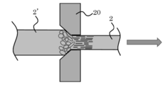
- the stretchable wiring sheet 10 A commercially available product may be used as the lead wire 2, but the strength and fatigue resistance of the lead wire 2 are improved by using the plastically processed material as described above, and thus the durability of the stretchable sheet 10. Can be improved. That is, as shown in FIG. 2, the heat-treated conductive wire forming material 2 ′ is drawn in the direction of the arrow by using a wire drawing die 20, so that random grains before processing are processed in the longitudinal direction after processing. It can be made into an elongated shape along the arrow direction in the figure, and the lead wire 2 can be formed so as to include a metal structure composed of crystal grains oriented in such a direction.
- FIG. 2 is explanatory drawing which shows the mode of a wire drawing process.
- layering that has been arranged in an arbitrary direction by conducting such wire drawing on a wire forming material containing a metal structure called pearlite structure after patenting (heat treatment)
- the ferrite and cementite of this form a fibrous metal structure arranged in the longitudinal direction.
- a metal structure in which fine needle-like or rod-like crystal grains are arranged in the longitudinal direction is obtained. .
- the tensile strength and the fatigue resistance are improved as the workability (area reduction ratio) represented by the following formula (1) is increased.
- the degree of processing of the conductive wire 2 is preferably 50% or more, more preferably 90% or more, and particularly preferably 95% or more.
- the upper limit of the workability is about 99%. If the workability exceeds the limit range (about 99%), the tensile strength and fatigue resistance are significantly lowered.
- d0 in said Formula (1) shows the diameter in the initial stage before letting the dice
- the final diameter of the formed conducting wire is shown.
- wire drawing has been described as an example, it is constituted by crystal grains that are elongated along the longitudinal direction by appropriately adjusting the direction in which pressure is applied also by other plastic processing such as rolling. It is possible to form a conductive wire including a metallic structure.
- said elongate shape the above-mentioned fiber shape, needle shape, and rod shape are included, and all the shapes elongated in one direction are included.
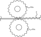
- FIG. 3 is explanatory drawing which shows a mode that a linear conducting wire is processed into a wave shape.
- the stretchable wiring sheet 10 is simply bonded to the first elastomer sheet 1a and the second elastomer sheet 1b with the conductive wire 2 plastically deformed so as to have the wavy shape in between. It can be manufactured easily and at low cost.
- a linear conductive wire is processed into the wavy shape, but instead of this method, a coiled conductive wire is processed into the wavy shape. Also good. That is, after extending a coil-shaped conducting wire to such an extent that the coil wires do not overlap each other, it is introduced into a rolling roller or the like and rolled from above and below to obtain the wavy-shaped conducting wire 2.
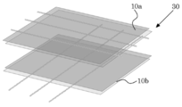
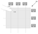
- FIG. 4A is an explanatory diagram illustrating a configuration example of the stretchable touch sensor sheet.
- the stretchable touch sensor sheet 30 is configured using two stretchable wiring sheets of the present invention. That is, the stretchable touch sensor sheet 30 has a transverse cross section between the stretchable first elastomer sheet and the stretchable second elastomer sheet that is bonded to face the first elastomer sheet.
- the cross-sectional shape is any one of a circular shape, an elliptical shape, and a track shape, and the lead wire plastically deformed into a wavy shape that is periodically curved along the longitudinal direction has a wave height of the wavy shape.
- the direction is arranged in a state along the in-plane direction of the opposing surfaces of the first elastomer sheet and the second elastomer sheet, and the first elastomer sheet and the second elastomer sheet are formed of a transparent material,
- Two stretchable wiring sheets 10a and 10b formed by arranging a plurality of conductive wires are arranged to face each other in a state in which the wiring directions of the conductive wires are orthogonal to each other.
- the stretchable touch sensor sheet 30 configured as described above is resistant to any shape change in the extending direction and the bending direction, and therefore flexibly deforms and follows the curved surface even when the installation location is a curved surface. In addition, it can be expected to exhibit excellent durability even when placed on a curved surface.
- the stretchable touch sensor sheet 30 can be used as a conductive sheet for a touch sensor such as a known resistance change type touch sensor or a capacitance type touch sensor.
- FIG. 4B shows a configuration example of a capacitive touch sensor.
- a capacitance change detection circuit is connected to one end portion of each conducting wire in an energized state and arranged in a vertical and horizontal matrix, and the elastic touch sensor sheet 30 of the touch operation is provided. Detect capacitance change.
- one conductor is configured as one detection line. However, when it is difficult to obtain an optimum resistance value for detection, one capacitance change is made for a plurality of conductors.
- a detection circuit can be connected to form one detection line.
- the material of the conductive wire is selected so that a change in resistance value during stretching is 5% or less. Moreover, it is preferable that the resistance value per unit length of one detection line is designed to be 100 ⁇ / cm or less. On the other hand, when the stretchable touch sensor sheet 30 is used for the capacitive touch sensor, it is preferable to select the material of the conductive wire so that the change in resistance value during stretching is 30% or less. Moreover, it is preferable that the resistance value per unit length of one detection line is designed to be 500 ⁇ / cm or less.
- the first elastomer sheet constituting the stretchable touch sensor sheet 30 in consideration of the visibility of dirt on the touch surface and the visibility of the image on the display when viewed through the touch sensor.
- the second elastomer sheet is required to have a transparency with a visible light transmittance of 50% or more in a state of being opposed to each other.
- the haze value (cloudiness value) of the stretchable touch sensor sheet 30 is preferably as small as possible (for example, 3%) from the viewpoint of transparency, and is preferably 60% at most. This haze value is measured by irradiating the sheet with visible light and measuring the ratio of diffuse transmitted light to total transmitted light.
- the haze value can be adjusted by the wire diameter of the conducting wire, the interval at which the conducting wires are arranged in parallel, and the like.
- the relationship between the wire diameter of the conducting wire and the distance to the touch sensor and the visibility is shown in Table 1 below.
- ⁇ indicates that it cannot be visually recognized by subjective evaluation
- ⁇ indicates that it can barely be visually recognized
- x indicates that it can be visually recognized.
- the wire diameter of the conducting wire is preferably 12 ⁇ m or less.
- the wire diameter of the conducting wire may be about 40 ⁇ m or less.
- the haze value is easily obtained when the interval at which the conducting wires are arranged in parallel is about 100 ⁇ m to 10 mm.
- the number of bending resistances when the radius of curvature of the wavy shape of the conductive wire is 1 mm is 100,000 times or more.
- the stretch rate is 50% or more and the bending resistance is 100,000 times. The above is preferable.
- the elongation rate is 60% or more and the resistance change rate of the conductor is 5% or less.
Landscapes
- Engineering & Computer Science (AREA)
- Theoretical Computer Science (AREA)
- General Engineering & Computer Science (AREA)
- Human Computer Interaction (AREA)
- Physics & Mathematics (AREA)
- General Physics & Mathematics (AREA)
- Microelectronics & Electronic Packaging (AREA)
- Mechanical Engineering (AREA)
- Computer Networks & Wireless Communication (AREA)
- Manufacturing & Machinery (AREA)
- Laminated Bodies (AREA)
- Insulated Conductors (AREA)
- Structure Of Printed Boards (AREA)
- Non-Insulated Conductors (AREA)
Abstract
Priority Applications (3)
| Application Number | Priority Date | Filing Date | Title |
|---|---|---|---|
| US16/070,580 US11259408B2 (en) | 2016-01-19 | 2017-01-05 | Stretchable wiring sheet and stretchable touch sensor sheet |
| JP2017562498A JP6901408B2 (ja) | 2016-01-19 | 2017-01-05 | 伸縮性配線シート及び伸縮性タッチセンサシート |
| EP17741205.3A EP3407686A4 (fr) | 2016-01-19 | 2017-01-05 | Feuille de câblage étirable et feuille de capteur tactile étirable |
Applications Claiming Priority (2)
| Application Number | Priority Date | Filing Date | Title |
|---|---|---|---|
| JP2016-007844 | 2016-01-19 | ||
| JP2016007844 | 2016-01-19 |
Publications (1)
| Publication Number | Publication Date |
|---|---|
| WO2017126325A1 true WO2017126325A1 (fr) | 2017-07-27 |
Family
ID=59361727
Family Applications (1)
| Application Number | Title | Priority Date | Filing Date |
|---|---|---|---|
| PCT/JP2017/000133 Ceased WO2017126325A1 (fr) | 2016-01-19 | 2017-01-05 | Feuille de câblage étirable et feuille de capteur tactile étirable |
Country Status (5)
| Country | Link |
|---|---|
| US (1) | US11259408B2 (fr) |
| EP (1) | EP3407686A4 (fr) |
| JP (1) | JP6901408B2 (fr) |
| TW (1) | TWI630850B (fr) |
| WO (1) | WO2017126325A1 (fr) |
Cited By (2)
| Publication number | Priority date | Publication date | Assignee | Title |
|---|---|---|---|---|
| KR20210013498A (ko) * | 2019-07-26 | 2021-02-04 | 인하대학교 산학협력단 | 응력 감소를 위한 기판 |
| CN119197638A (zh) * | 2024-09-20 | 2024-12-27 | 国网湖北省电力有限公司黄石供电公司 | 一种架设高压电缆智能监测方法及系统 |
Families Citing this family (4)
| Publication number | Priority date | Publication date | Assignee | Title |
|---|---|---|---|---|
| WO2020105206A1 (fr) * | 2018-11-22 | 2020-05-28 | 株式会社村田製作所 | Carte de circuit imprimé souple, et procédé pour la fabrication d'une carte de circuit imprimé souple |
| KR102706332B1 (ko) * | 2018-12-26 | 2024-09-11 | 엘지디스플레이 주식회사 | 터치 패널 및 이를 포함하는 스트레쳐블 표시장치 |
| CN210670181U (zh) * | 2020-01-21 | 2020-06-02 | 湃瑞电子科技(苏州)有限公司 | 一种装置及其触控屏和手机 |
| CN115684722A (zh) * | 2022-09-06 | 2023-02-03 | 无锡宝通智能物联科技有限公司 | 输送带感知层电极及其制作方法及应用 |
Citations (11)
| Publication number | Priority date | Publication date | Assignee | Title |
|---|---|---|---|---|
| JPH08201785A (ja) * | 1995-01-31 | 1996-08-09 | Teijin Ltd | 透明導電性フィルム |
| JP2005191113A (ja) * | 2003-12-24 | 2005-07-14 | Kyocera Corp | 配線基板及び電気装置並びにその製造方法 |
| WO2009102077A1 (fr) | 2008-02-11 | 2009-08-20 | The University Of Tokyo | Composition de caoutchouc à nanotube de carbone, câblage, pâte électroconductrice, circuit électronique et procédé de fabrication de la composition de caoutchouc à nanotube de carbone |
| JP2011034822A (ja) | 2009-08-03 | 2011-02-17 | Tokai Rubber Ind Ltd | 配線体接続構造体およびその製造方法 |
| JP2013084842A (ja) * | 2011-10-12 | 2013-05-09 | Fujitsu Ltd | 配線構造及びその製造方法 |
| JP2013089910A (ja) * | 2011-10-21 | 2013-05-13 | Fujikura Ltd | フレキシブルプリント基板及びその製造方法 |
| JP2013187308A (ja) | 2012-03-07 | 2013-09-19 | Nippon Mektron Ltd | 伸縮性フレキシブル回路基板 |
| JP2013187380A (ja) | 2012-03-08 | 2013-09-19 | Nippon Mektron Ltd | 伸縮性フレキシブル回路基板およびその製造方法 |
| JP2013206080A (ja) | 2012-03-28 | 2013-10-07 | Toppan Forms Co Ltd | 非接触型データ受送信体 |
| JP2015018494A (ja) * | 2013-07-12 | 2015-01-29 | 富士フイルム株式会社 | 配線基板 |
| JP2015197382A (ja) * | 2014-04-01 | 2015-11-09 | バンドー化学株式会社 | 静電容量型センサ、及び歪み計測装置 |
Family Cites Families (14)
| Publication number | Priority date | Publication date | Assignee | Title |
|---|---|---|---|---|
| JP3384398B2 (ja) * | 2000-05-25 | 2003-03-10 | セイコーエプソン株式会社 | 液晶装置、その製造方法および電子機器 |
| KR100548114B1 (ko) | 2000-12-21 | 2006-02-02 | 가부시키가이샤 히타치세이사쿠쇼 | 땜납 박 및 반도체 장치 및 전자 장치 |
| US7019734B2 (en) * | 2002-07-17 | 2006-03-28 | 3M Innovative Properties Company | Resistive touch sensor having microstructured conductive layer |
| US7491892B2 (en) * | 2003-03-28 | 2009-02-17 | Princeton University | Stretchable and elastic interconnects |
| TWI339087B (en) | 2007-04-18 | 2011-03-11 | Ind Tech Res Inst | Stretchable flexible printed circuit (fpc) and fabricating method thereof |
| WO2009057637A1 (fr) * | 2007-10-31 | 2009-05-07 | Sumitomo Metal Mining Co., Ltd. | Film conducteur transparent flexible et dispositif fonctionnel flexible l'utilisant |
| TWI370714B (en) | 2008-01-09 | 2012-08-11 | Ind Tech Res Inst | Circuit structure and menufacturing method thereof |
| TW201005609A (en) | 2008-07-22 | 2010-02-01 | Chi Hsin Electronics Corp | Touch panel |
| JP2013084571A (ja) * | 2011-09-29 | 2013-05-09 | Fujifilm Corp | 透明導電性塗布膜、透明導電性インク、及びそれらを用いたタッチパネル |
| WO2013063445A2 (fr) * | 2011-10-28 | 2013-05-02 | President And Fellows Of Harvard College | Accéléromètres et capteurs tactiles basé sur de papier, capacitifs |
| US9601557B2 (en) | 2012-11-16 | 2017-03-21 | Apple Inc. | Flexible display |
| JP2014173065A (ja) * | 2013-03-12 | 2014-09-22 | Nitto Denko Corp | 粘着剤、粘着剤層、粘着シート、及びタッチパネル |
| JP2015045623A (ja) | 2013-08-29 | 2015-03-12 | バンドー化学株式会社 | 静電容量型センサシート及び静電容量型センサ |
| KR20160139320A (ko) * | 2015-05-27 | 2016-12-07 | 엘지전자 주식회사 | 변형 가능한 디스플레이 장치 및 그의 동작 방법 |
-
2017
- 2017-01-05 US US16/070,580 patent/US11259408B2/en active Active
- 2017-01-05 EP EP17741205.3A patent/EP3407686A4/fr not_active Withdrawn
- 2017-01-05 WO PCT/JP2017/000133 patent/WO2017126325A1/fr not_active Ceased
- 2017-01-05 JP JP2017562498A patent/JP6901408B2/ja active Active
- 2017-01-18 TW TW106101635A patent/TWI630850B/zh active
Patent Citations (11)
| Publication number | Priority date | Publication date | Assignee | Title |
|---|---|---|---|---|
| JPH08201785A (ja) * | 1995-01-31 | 1996-08-09 | Teijin Ltd | 透明導電性フィルム |
| JP2005191113A (ja) * | 2003-12-24 | 2005-07-14 | Kyocera Corp | 配線基板及び電気装置並びにその製造方法 |
| WO2009102077A1 (fr) | 2008-02-11 | 2009-08-20 | The University Of Tokyo | Composition de caoutchouc à nanotube de carbone, câblage, pâte électroconductrice, circuit électronique et procédé de fabrication de la composition de caoutchouc à nanotube de carbone |
| JP2011034822A (ja) | 2009-08-03 | 2011-02-17 | Tokai Rubber Ind Ltd | 配線体接続構造体およびその製造方法 |
| JP2013084842A (ja) * | 2011-10-12 | 2013-05-09 | Fujitsu Ltd | 配線構造及びその製造方法 |
| JP2013089910A (ja) * | 2011-10-21 | 2013-05-13 | Fujikura Ltd | フレキシブルプリント基板及びその製造方法 |
| JP2013187308A (ja) | 2012-03-07 | 2013-09-19 | Nippon Mektron Ltd | 伸縮性フレキシブル回路基板 |
| JP2013187380A (ja) | 2012-03-08 | 2013-09-19 | Nippon Mektron Ltd | 伸縮性フレキシブル回路基板およびその製造方法 |
| JP2013206080A (ja) | 2012-03-28 | 2013-10-07 | Toppan Forms Co Ltd | 非接触型データ受送信体 |
| JP2015018494A (ja) * | 2013-07-12 | 2015-01-29 | 富士フイルム株式会社 | 配線基板 |
| JP2015197382A (ja) * | 2014-04-01 | 2015-11-09 | バンドー化学株式会社 | 静電容量型センサ、及び歪み計測装置 |
Non-Patent Citations (1)
| Title |
|---|
| See also references of EP3407686A4 |
Cited By (3)
| Publication number | Priority date | Publication date | Assignee | Title |
|---|---|---|---|---|
| KR20210013498A (ko) * | 2019-07-26 | 2021-02-04 | 인하대학교 산학협력단 | 응력 감소를 위한 기판 |
| KR102364739B1 (ko) | 2019-07-26 | 2022-02-21 | 인하대학교 산학협력단 | 응력 감소를 위한 기판 |
| CN119197638A (zh) * | 2024-09-20 | 2024-12-27 | 国网湖北省电力有限公司黄石供电公司 | 一种架设高压电缆智能监测方法及系统 |
Also Published As
| Publication number | Publication date |
|---|---|
| JP6901408B2 (ja) | 2021-07-14 |
| JPWO2017126325A1 (ja) | 2019-02-14 |
| EP3407686A4 (fr) | 2019-08-21 |
| EP3407686A1 (fr) | 2018-11-28 |
| TWI630850B (zh) | 2018-07-21 |
| US11259408B2 (en) | 2022-02-22 |
| TW201729653A (zh) | 2017-08-16 |
| US20200396832A1 (en) | 2020-12-17 |
Similar Documents
| Publication | Publication Date | Title |
|---|---|---|
| JP6901408B2 (ja) | 伸縮性配線シート及び伸縮性タッチセンサシート | |
| TWI620663B (zh) | 伸縮性配線片材以及其製造方法及製造裝置、伸縮性觸碰感測片 | |
| JP6666806B2 (ja) | 伸縮性配線シート及びその製造方法、伸縮性タッチセンサシート | |
| Gonzalez et al. | Design of metal interconnects for stretchable electronic circuits | |
| US9814134B2 (en) | Elastic flexible substrate and manufacturing method thereof | |
| JP6377241B2 (ja) | 高伸縮性配線及びその製造方法、製造装置 | |
| KR20180061003A (ko) | 전도성 유연 소자 | |
| CN112435589B (zh) | 显示面板和显示终端 | |
| JP7252529B2 (ja) | 伸縮配線部材 | |
| KR20200020429A (ko) | 픽셀형 압력센서 및 그의 제조방법 | |
| Li et al. | A stretchable knitted interconnect for three-dimensional curvilinear surfaces | |
| US10393599B2 (en) | Deformable apparatus and method | |
| EP3063308A1 (fr) | Conducteur d'alliage à mémoire de forme résistant à la déformation plastique | |
| Zhilyaeva et al. | Tunable force sensor based on carbon nanotube fiber for fine mechanical and acoustic technologies | |
| US9486619B2 (en) | Interconnect devices, systems, and methods for bridging electronic devices | |
| CN106618637A (zh) | 穿戴式超声波感测装置 | |
| KR20180072953A (ko) | 정전용량형 압력센서 및 그의 제조방법 | |
| Hwang et al. | Signal-amplified stretchable PVDF kirigami sensor via neutral axis modification | |
| KR20200042576A (ko) | 웨어러블 디바이스용 신축성 전도체, 그 신축성 전도체를 이용한 연결장치, 유연전극, 전자소자 및 그 제조방법 | |
| JP2019075416A (ja) | 配線基板及び配線基板の製造方法 | |
| CN107437534A (zh) | 可拉伸电子系统 | |
| CN213339729U (zh) | 线缆和具有该线缆的电子设备 | |
| CN119509330A (zh) | 一种可测量应变方向及应变大小的三维柔性传感结构及其制备方法和应用 | |
| JP2017078703A (ja) | 変形測定装置 |
Legal Events
| Date | Code | Title | Description |
|---|---|---|---|
| 121 | Ep: the epo has been informed by wipo that ep was designated in this application |
Ref document number: 17741205 Country of ref document: EP Kind code of ref document: A1 |
|
| ENP | Entry into the national phase |
Ref document number: 2017562498 Country of ref document: JP Kind code of ref document: A |
|
| NENP | Non-entry into the national phase |
Ref country code: DE |
|
| WWE | Wipo information: entry into national phase |
Ref document number: 2017741205 Country of ref document: EP |
|
| ENP | Entry into the national phase |
Ref document number: 2017741205 Country of ref document: EP Effective date: 20180820 |