WO2017141663A1 - Dispositif de communication sans fil et son procédé de fabrication - Google Patents
Dispositif de communication sans fil et son procédé de fabrication Download PDFInfo
- Publication number
- WO2017141663A1 WO2017141663A1 PCT/JP2017/002888 JP2017002888W WO2017141663A1 WO 2017141663 A1 WO2017141663 A1 WO 2017141663A1 JP 2017002888 W JP2017002888 W JP 2017002888W WO 2017141663 A1 WO2017141663 A1 WO 2017141663A1
- Authority
- WO
- WIPO (PCT)
- Prior art keywords
- wireless communication
- communication device
- circuit board
- element block
- plating
- Prior art date
- Legal status (The legal status is an assumption and is not a legal conclusion. Google has not performed a legal analysis and makes no representation as to the accuracy of the status listed.)
- Ceased
Links
Images


Classifications
-
- G—PHYSICS
- G06—COMPUTING OR CALCULATING; COUNTING
- G06K—GRAPHICAL DATA READING; PRESENTATION OF DATA; RECORD CARRIERS; HANDLING RECORD CARRIERS
- G06K19/00—Record carriers for use with machines and with at least a part designed to carry digital markings
- G06K19/02—Record carriers for use with machines and with at least a part designed to carry digital markings characterised by the selection of materials, e.g. to avoid wear during transport through the machine
-
- G—PHYSICS
- G06—COMPUTING OR CALCULATING; COUNTING
- G06K—GRAPHICAL DATA READING; PRESENTATION OF DATA; RECORD CARRIERS; HANDLING RECORD CARRIERS
- G06K19/00—Record carriers for use with machines and with at least a part designed to carry digital markings
- G06K19/06—Record carriers for use with machines and with at least a part designed to carry digital markings characterised by the kind of the digital marking, e.g. shape, nature, code
- G06K19/067—Record carriers with conductive marks, printed circuits or semiconductor circuit elements, e.g. credit or identity cards also with resonating or responding marks without active components
- G06K19/07—Record carriers with conductive marks, printed circuits or semiconductor circuit elements, e.g. credit or identity cards also with resonating or responding marks without active components with integrated circuit chips
- G06K19/077—Constructional details, e.g. mounting of circuits in the carrier
-
- H—ELECTRICITY
- H01—ELECTRIC ELEMENTS
- H01P—WAVEGUIDES; RESONATORS, LINES, OR OTHER DEVICES OF THE WAVEGUIDE TYPE
- H01P11/00—Apparatus or processes specially adapted for manufacturing waveguides or resonators, lines, or other devices of the waveguide type
-
- H—ELECTRICITY
- H01—ELECTRIC ELEMENTS
- H01Q—ANTENNAS, i.e. RADIO AERIALS
- H01Q7/00—Loop antennas with a substantially uniform current distribution around the loop and having a directional radiation pattern in a plane perpendicular to the plane of the loop
-
- H—ELECTRICITY
- H05—ELECTRIC TECHNIQUES NOT OTHERWISE PROVIDED FOR
- H05K—PRINTED CIRCUITS; CASINGS OR CONSTRUCTIONAL DETAILS OF ELECTRIC APPARATUS; MANUFACTURE OF ASSEMBLAGES OF ELECTRICAL COMPONENTS
- H05K1/00—Printed circuits
- H05K1/02—Details
- H05K1/11—Printed elements for providing electric connections to or between printed circuits
-
- H—ELECTRICITY
- H05—ELECTRIC TECHNIQUES NOT OTHERWISE PROVIDED FOR
- H05K—PRINTED CIRCUITS; CASINGS OR CONSTRUCTIONAL DETAILS OF ELECTRIC APPARATUS; MANUFACTURE OF ASSEMBLAGES OF ELECTRICAL COMPONENTS
- H05K3/00—Apparatus or processes for manufacturing printed circuits
-
- H—ELECTRICITY
- H05—ELECTRIC TECHNIQUES NOT OTHERWISE PROVIDED FOR
- H05K—PRINTED CIRCUITS; CASINGS OR CONSTRUCTIONAL DETAILS OF ELECTRIC APPARATUS; MANUFACTURE OF ASSEMBLAGES OF ELECTRICAL COMPONENTS
- H05K3/00—Apparatus or processes for manufacturing printed circuits
- H05K3/10—Apparatus or processes for manufacturing printed circuits in which conductive material is applied to the insulating support in such a manner as to form the desired conductive pattern
- H05K3/18—Apparatus or processes for manufacturing printed circuits in which conductive material is applied to the insulating support in such a manner as to form the desired conductive pattern using precipitation techniques to apply the conductive material
-
- H—ELECTRICITY
- H10—SEMICONDUCTOR DEVICES; ELECTRIC SOLID-STATE DEVICES NOT OTHERWISE PROVIDED FOR
- H10W—GENERIC PACKAGES, INTERCONNECTIONS, CONNECTORS OR OTHER CONSTRUCTIONAL DETAILS OF DEVICES COVERED BY CLASS H10
- H10W74/00—Encapsulations, e.g. protective coatings
- H10W74/01—Manufacture or treatment
-
- H—ELECTRICITY
- H10—SEMICONDUCTOR DEVICES; ELECTRIC SOLID-STATE DEVICES NOT OTHERWISE PROVIDED FOR
- H10W—GENERIC PACKAGES, INTERCONNECTIONS, CONNECTORS OR OTHER CONSTRUCTIONAL DETAILS OF DEVICES COVERED BY CLASS H10
- H10W90/00—Package configurations
-
- H—ELECTRICITY
- H10—SEMICONDUCTOR DEVICES; ELECTRIC SOLID-STATE DEVICES NOT OTHERWISE PROVIDED FOR
- H10W—GENERIC PACKAGES, INTERCONNECTIONS, CONNECTORS OR OTHER CONSTRUCTIONAL DETAILS OF DEVICES COVERED BY CLASS H10
- H10W44/00—Electrical arrangements for controlling or matching impedance
- H10W44/20—Electrical arrangements for controlling or matching impedance at high-frequency [HF] or radio frequency [RF]
- H10W44/241—Electrical arrangements for controlling or matching impedance at high-frequency [HF] or radio frequency [RF] for passive devices or passive elements
- H10W44/248—Electrical arrangements for controlling or matching impedance at high-frequency [HF] or radio frequency [RF] for passive devices or passive elements for antennas
-
- H—ELECTRICITY
- H10—SEMICONDUCTOR DEVICES; ELECTRIC SOLID-STATE DEVICES NOT OTHERWISE PROVIDED FOR
- H10W—GENERIC PACKAGES, INTERCONNECTIONS, CONNECTORS OR OTHER CONSTRUCTIONAL DETAILS OF DEVICES COVERED BY CLASS H10
- H10W70/00—Package substrates; Interposers; Redistribution layers [RDL]
- H10W70/60—Insulating or insulated package substrates; Interposers; Redistribution layers
- H10W70/62—Insulating or insulated package substrates; Interposers; Redistribution layers characterised by their interconnections
- H10W70/63—Vias, e.g. via plugs
-
- H—ELECTRICITY
- H10—SEMICONDUCTOR DEVICES; ELECTRIC SOLID-STATE DEVICES NOT OTHERWISE PROVIDED FOR
- H10W—GENERIC PACKAGES, INTERCONNECTIONS, CONNECTORS OR OTHER CONSTRUCTIONAL DETAILS OF DEVICES COVERED BY CLASS H10
- H10W90/00—Package configurations
- H10W90/701—Package configurations characterised by the relative positions of pads or connectors relative to package parts
- H10W90/721—Package configurations characterised by the relative positions of pads or connectors relative to package parts of bump connectors
- H10W90/724—Package configurations characterised by the relative positions of pads or connectors relative to package parts of bump connectors between a chip and a stacked insulating package substrate, interposer or RDL
Definitions
- the present invention relates to a wireless communication device used in a short-range wireless communication apparatus including an RFID (Radio Frequency Identification) tag.
- RFID Radio Frequency Identification
- a coil antenna is formed by connecting a plurality of conductors such as a lower conductor, a side conductor, an upper conductor, and an interlayer conductor formed in an insulating layer.
- the present invention solves the above-described problems, and an object of the present invention is to provide a wireless communication device that can improve the connection reliability of a coil antenna, and a manufacturing method thereof.
- a method of manufacturing a wireless communication device of one aspect of the present invention includes: Preparing a circuit board comprising: an RFIC element mounted on the first surface; and an interlayer conductor extending from the first surface to a second surface opposite to the first surface and connected to the RFIC element; Covering at least the first surface of the circuit board with an element block; Providing a coiled conductor that goes around the circuit board and the element block, and forming a coil antenna connected to the RFIC element via the interlayer conductor; including.
- a wireless communication device of one embodiment of the present invention includes: A circuit board comprising: an RFIC element mounted on a first surface; and an interlayer conductor extending from the first surface to a second surface opposite to the first surface and connected to the RFIC element; An element block covering at least the first surface of the circuit board; A coil antenna connected to the RFIC element via the interlayer conductor and formed of a coiled conductor that goes around the circuit board and the element block; Is provided.
- the present invention it is possible to provide a wireless communication device capable of improving the connection reliability of a coil antenna and a method for manufacturing the same.
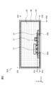
- FIG. 1 is a perspective view of a wireless communication device according to a first embodiment of the present invention.
- 1 is a schematic configuration diagram of a wireless communication device according to a first embodiment of the present invention.
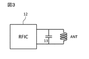
- 1 is a circuit diagram of a wireless communication device according to a first embodiment of the present invention.
- FIG. 3 is a perspective view of the wireless communication device according to the second embodiment of the present invention. Schematic configuration diagram of a wireless communication device according to a second embodiment of the present invention The figure which shows the manufacturing process of the radio
- FIG. 3 is a perspective view of a wireless communication device according to a third embodiment of the present invention.
- Partial enlarged view of a wireless communication device according to a third embodiment of the present invention Schematic configuration diagram of a wireless communication device according to a third embodiment of the present invention
- a perspective view of a wireless communication device according to a fourth embodiment of the present invention Schematic configuration diagram of a wireless communication device according to a fourth embodiment of the present invention The figure which shows the manufacturing process of the radio
- FIG. 4 The figure which shows the manufacturing process of the radio
- Schematic configuration diagram of a wireless communication device according to a fifth embodiment of the present invention A perspective view of an article with a wireless communication device according to a sixth embodiment of the present invention.
- wireless communication device of Embodiment 7 which concerns on this invention The figure which shows the manufacturing process of the radio
- a coil antenna is formed by connecting a plurality of conductors through a plurality of different processes. Since the plurality of conductors are formed and connected in different processes, an interface is formed at a place where the conductors are connected. The present inventors have found that the connection reliability of the coil antenna is reduced at this interface. Accordingly, the present inventors have reached the following invention in order to improve the connection reliability of the coil antenna.
- a method of manufacturing a wireless communication device of one aspect of the present invention includes: Preparing a circuit board comprising: an RFIC element mounted on the first surface; and an interlayer conductor extending from the first surface to a second surface opposite to the first surface and connected to the RFIC element; Covering at least the first surface of the circuit board with an element block; Providing a coiled conductor that goes around the circuit board and the element block, and forming a coil antenna connected to the RFIC element via the interlayer conductor; including.
- the coil antenna is formed by the coiled conductor that circulates around the circuit board and the element block, it is possible to manufacture a wireless communication device having a coil antenna with improved connection reliability.
- the step of covering the circuit board with the element block may embed the circuit board in the element block.
- the step of preparing the circuit board includes preparing a mother board in which a plurality of circuit boards are continuously provided,
- the step of covering the circuit board with the element block covers the mother substrate with the element block,
- the step of forming the coil antenna includes a plurality of coil-shaped conductors that circulate between the element block and the mother board, with a direction in which the plurality of circuit boards are continuous as a winding axis direction.
- the coiled conductor may be a plating pattern.
- a wireless communication device having a coil antenna whose connection reliability is improved by a plating pattern can be easily manufactured.
- the step of forming the coil antenna includes the step of activating the pattern formation region of the circuit board and the element block by laser processing and forming the plating pattern by forming a plating film in the pattern formation region. May be included.
- the step of forming the plating pattern may include a step of performing electrolytic plating.
- the plating pattern can be grown even thicker.
- the element block may include a plating core material.
- the plating pattern can be formed more easily by laser processing.
- the plating pattern can be formed more easily and at low cost by performing laser processing on the thick film layer.
- the coiled conductor may be a metal wire.
- Such a configuration can reduce the resistance of the coil antenna itself.
- the coiled conductor may be a spring material.
- a wireless communication device of one embodiment of the present invention includes: A circuit board comprising: an RFIC element mounted on a first surface; and an interlayer conductor extending from the first surface to a second surface opposite to the first surface and connected to the RFIC element; An element block covering at least the first surface of the circuit board; A coil antenna connected to the RFIC element via the interlayer conductor and formed of a coiled conductor that goes around the circuit board and the element block; Is provided.
- the coil antenna is formed by the coiled conductor that circulates around the circuit board and the element block, the connection reliability of the coil antenna can be improved.
- the circuit board may be embedded in the element block.
- the circuit board is not exposed to the outside of the element block, so that the heat resistance can be improved.
- the interlayer conductor may be a metal pin.
- the direct current resistance component can be made smaller than that of the sintered metal body or the conductor film, so that the loss due to the interlayer conductor can be reduced.
- the coiled conductor may be a plating pattern.
- Such a configuration can improve the connection reliability of the coil antenna.
- the coiled conductor may be a metal wire.
- Such a configuration can reduce the resistance of the coil antenna itself.
- the coiled conductor may be a spring material.
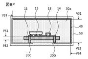
- FIG. 1 is a perspective view of a wireless communication device 10A according to the first embodiment of the present invention.
- the X-axis direction indicates the width direction of the wireless communication device 10A
- the Y-axis direction indicates the thickness direction of the wireless communication device 10A
- the Z-axis direction indicates the wireless communication device.
- the height direction of 10A is shown.
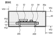
- FIG. 2 is a schematic configuration diagram of the wireless communication device 10A.
- the wireless communication device 10 ⁇ / b> A includes a circuit board 11, a body block 30 that covers the circuit board 11, and a coil antenna formed by a plating pattern 40 that goes around the circuit board 11 and the body block 30. And comprising.
- the plating pattern 40 is prevented from being oxidized from above the coil antenna, the impact resistance and heat resistance of the wireless communication device itself, Is formed with a protective layer 50 for improving moldability during resin embedding.
- the side surface of the circuit board 11 is exposed from the end surface in the Y-axis direction of the element block 30, this side surface may also be covered with the element block 30.
- the circuit board 11 has a first surface PS1, a second surface PS2 facing the first surface PS1, and four side surfaces connected to the first surface PS1 and the second surface PS2. It is a flat printed wiring board having a rectangular shape in plan view. As shown in FIG. 2, a wiring conductor pattern 14 is formed on the first surface PS ⁇ b> 1 of the circuit board 11. On the first surface PS ⁇ b> 1 of the circuit board 11, the RFIC element 12, the chip capacitor 13, and the like are mounted on the wiring conductor pattern 14.
- the circuit board 11 includes interlayer conductors 20A and 20B extending from the first surface PS1 to the second surface PS2, that is, in the Z-axis direction.
- the interlayer conductors 20 ⁇ / b> A and 20 ⁇ / b> B are electrically connected to the RFIC element 12 and the chip capacitor 13 through the wiring conductor pattern 14 and are also electrically connected to a coil antenna formed by the plating pattern 40.
- the circuit board 11 may be, for example, a glass epoxy board or a resin board, or may be a ceramic board formed with a thick film pattern.
- the wiring conductor pattern 14 is patterned, for example, by etching a copper foil.
- the RFIC element 12 is, for example, a packaged RFIC chip (bare chip) having input / output terminals.
- the RFIC chip is an IC chip on which an RF circuit, a memory circuit, a control circuit, etc. for an RFID system are mounted.
- the chip capacitor 13 is, for example, a multilayer ceramic chip component.
- the interlayer conductors 20A and 20B are, for example, metal columnar bodies such as through-hole conductors by plating or the like, sintered metal bodies by firing of conductive paste, or thin-film metal bodies by etching of conductive thin films.
- the element block 30 is made of a resin member that covers the first surface PS1 of the circuit board 11 and protects mounting components such as the RFIC element 12 mounted on the first surface PS1 of the circuit board 11. This resin member is also preferably a resin member having heat resistance against heat when the device is embedded in a resin molding.
- the element block 30 is a resin block, and is made of, for example, a resin member made of an epoxy resin or the like. As shown in FIG. 1, the element block 30 has a rectangular parallelepiped shape. Specifically, the element block 30 includes a first main surface VS1, a second main surface VS2 facing the first main surface VS1, and a first main surface VS1 and a second main surface VS2.
- the second main surface VS2 of the element body block 30 is flush with the second surface PS2 of the circuit board 11, as shown in FIG. That is, a part of the second main surface VS ⁇ b> 2 of the element block 30 is formed by the second surface PS ⁇ b> 2 of the circuit board 11.
- the coil antenna is formed by a plating pattern 40 that circulates the circuit board 11 and the element block 30 around the winding axis direction, that is, the Y-axis direction.
- the plating pattern 40 is not limited, for example, it is formed in a 6-turn rectangular helical shape.
- One end of the plating pattern 40 is connected to the interlayer conductor 20 ⁇ / b> A of the circuit board 11.
- the other end of the plating pattern 40 is connected to the interlayer conductor 20 ⁇ / b> B of the circuit board 11.
- the plating pattern 40 extends from the end portion of the interlayer conductor 20A on the second surface PS2 of the circuit board 11, circulates around the outer peripheral surface of the circuit board 11 and the element block 30, and the interlayer conductor of the second surface PS2 of the circuit board 11 Connected to the end of 20B. More specifically, the plating pattern 40 extends from the end portion of the interlayer conductor 20A and circulates in the order of the second main surface VS2, the first side surface VS3, the first main surface VS1, and the second side surface VS4 of the element block 30. , Connected to the end of the interlayer conductor 20B.
- the plating pattern 40 extends in the X-axis direction on the first main surface VS1 and the second main surface VS2, and extends in the Z-axis direction on the first side surface VS3 and the second side surface VS4.
- “extending in the X-axis direction” does not limit that the extending direction of the plating pattern 40 that circulates around the circuit board 11 and the element block 30 is parallel to the X-axis direction.
- the extending direction of 40 includes a direction extending substantially in the X-axis direction.
- “extending in the Z-axis direction” does not limit that the extending direction of the plating pattern 40 that goes around the circuit board 11 and the element block 30 is parallel to the Z-axis direction.
- the extending direction of 40 includes a direction extending substantially in the Z-axis direction.
- the plating pattern 40 is preferably made of a material having a small specific resistance mainly composed of nickel or copper. Moreover, you may have the multilayer structure which has 2nd plating films, such as tin or gold
- FIG. 3 is a circuit diagram of the wireless communication device 10A.
- a coil antenna ANT is connected to the RFIC element 12.
- a chip capacitor 13 is connected in parallel to the coil antenna ANT.
- An antenna resonance circuit having a resonance frequency in the HF band is configured by the coil antenna ANT, the chip capacitor 13, and the capacitance component of the RFIC element 12 itself. Accordingly, the wireless communication device 10A is configured as an HF band RFID tag.
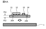
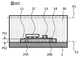
- FIGS. 4A to 4F are diagrams sequentially illustrating the manufacturing process of the wireless communication device 10A.
- a circuit board 11 is prepared in which an RFIC element 12 and a chip capacitor 13 are mounted on a wiring conductor pattern 14 provided on the first surface PS1 side, and interlayer conductors 20A and 20B are provided therein. To do.
- the circuit board 11 is arranged on the base 1 with the second surface PS2 side as a lower surface.
- An adhesive layer (not shown) is provided on the pedestal 1, and the second surface PS2 side of the circuit board 11 is in contact with the adhesive layer. That is, the circuit board 11 is fixed to the adhesive layer of the base 1.
- the adhesive layer is, for example, a resin having adhesiveness.
- the circuit board 11 on the pedestal 1 is covered with the element block 30.
- the element block 30 is formed, for example, by applying a liquid thermosetting resin on the pedestal 1 on which the circuit board 11 is disposed, and curing it by heat treatment.
- the element block 30 may be formed by covering a circuit board 11 with a semi-cured resin sheet and curing it.
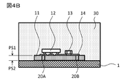
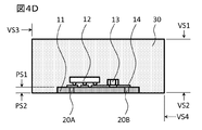
- the base 1 is removed, and the upper surface and the lower surface of the element block 30 are polished.
- the element block 30 is polished to predetermined polishing positions P1 and P2 by, for example, buffing or scribing.
- the upper surface of the element body block 30 is a surface on the first main surface VS1 side
- the lower surface of the element body block 30 is a surface on the second main surface VS2 side.
- the upper surface of the element block 30 is polished to a predetermined polishing position P1 so as to be flat. In addition, if the upper surface of the element block 30 is in a flat state before polishing, the polishing may not be performed.
- the lower surface of the element block 30 is polished together with the circuit board 11 to a predetermined polishing position P2. Further, by polishing the second surface PS2 of the circuit board 11, the end portions of the interlayer conductors 20A and 20B are exposed. When the lower surface of the element block 30 is polished, the entire base 1 may be polished without removing the base 1.
- the predetermined polishing positions P1, P2 may be determined based on the dimensions of the wireless communication device 10A to be manufactured.
- the upper and lower surfaces of the element block 30 can be flattened as shown in FIG. 4D.
- the size of the wireless communication device 10A can be adjusted by adjusting the predetermined polishing positions P1 and P2.
- the corners of the element block 30 are preferably chamfered. By chamfering the corners of the element block 30, laser processing and wiring pattern formation described later can be performed smoothly.
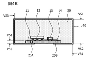
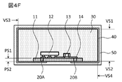
- a coil antenna is formed by a plating pattern 40 that circulates between the circuit board 11 and the element block 30 while being connected to the interlayer conductors 20A and 20B of the circuit board 11.
- the plating pattern 40 is formed using a processing technique such as MID (Molded Interconnect Device).
- the pattern formation region of the circuit board 11 and the element block 30 is activated by ablation by laser processing, and the plating pattern 40 is formed by forming a plating film in this pattern formation region. .
- the portion of the circuit board 11 and the element block 30 where the plating pattern 40 is to be formed is irradiated with laser.
- Laser irradiation is performed from the end of the interlayer conductor 20A exposed at the second surface PS2 of the circuit board 11 through the second main surface VS2, the first side surface VS3, the first main surface VS1, and the second side surface VS4 of the element block 30.
- the laser is irradiated while rotating around the element block 30 clockwise around the winding axis of the coil antenna, that is, the Y-axis direction (see FIG. 1).
- a plating pattern 40 is formed by forming a plating film on the portion irradiated with the laser.
- a coil antenna can be formed by performing electroless plating and forming the continuous plating pattern 40 in the laser irradiated part. Furthermore, electrolytic plating may be performed to increase the film thickness of the pattern.
- a protective layer 50 is formed on the surface of the circuit board 11 and the element block 30 from above the plating pattern 40.
- the protective layer 50 is provided to protect the coil antenna.
- the protective layer 50 is a protective resin film for preventing oxidation of the plating pattern 40, impact resistance and heat resistance of the wireless communication device itself, and improving moldability at the time of resin embedding. It is a solder resist film.
- the wireless communication device 10A is manufactured by performing the steps shown in FIGS. 4A to 4F. These steps may be processing steps of individual wireless communication devices, but in the present embodiment, processing is performed in a collective substrate state in which a plurality of wireless communication devices are assembled.
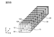
- 5A and 5B show a manufacturing process of the wireless communication device 10A using a rod-shaped aggregate substrate.
- a mother board 90 on which a plurality of circuit boards 11 are continuously provided in a row is fixed on the base 1.
- the mother board 90 the plurality of circuit boards 11 are provided in a row continuously in the Y-axis direction.
- the plurality of circuit boards 11 may be independent.
- the mother substrate 90 fixed on the base 1 is covered with the element block 30.
- the base 1 is removed, and the upper and lower surfaces of the element block 30 are flattened by surface polishing.
- the pattern formation region is irradiated with laser.
- the laser irradiation is performed while circulating around the mother substrate 90 with the direction in which the plurality of circuit boards 11 are continuous, that is, the Y-axis direction as an axial direction.
- electroless plating is performed to form a plurality of plating patterns 40 in the laser irradiated portion.
- a plurality of coil antennas connected to each of the plurality of circuit boards 11 are formed by the plurality of plating patterns 40 that circulate around the mother substrate 90 and the element block 30 around the winding axis.
- the substrate is produced in a collective substrate state in which a plurality of wireless communication devices 10A are connected in the winding axis direction, that is, the Y-axis direction.
- the collective substrate is cut in a direction intersecting the winding axis direction, that is, in the X-axis direction or the Z-axis direction in FIG. Divide into pieces. Accordingly, the individual wireless communication device 10A is acquired from the collective substrate.
- the coil antenna is formed by the plating pattern 40 that goes around the circuit board 11 and the element block 30.
- wireless communication devices is not formed by connecting a some conductor, generation
- the coil antenna has a rectangular cross-sectional shape when viewed from the Y-axis direction.
- stress due to heat or impact is likely to be applied to the four corners, but at least the patterns including the four corners are continuous with the same material. Therefore, the risk of disconnection at this portion can be greatly reduced.
- the wireless communication device 10A when the wireless communication device 10A is embedded in a resin molded article, the reliability of the wireless communication device 10A is not impaired even if the wireless communication device 10A comes into contact with a resin having a high temperature (for example, 300 ° C. or higher instantaneously) that flows during injection molding. . That is, the wireless communication device 10A has excellent heat resistance.
- a resin having a high temperature for example, 300 ° C. or higher instantaneously
- the first surface PS1 side of the circuit board 11 is covered with the element block 30. That is, a surface mount component such as an RFIC element or a chip capacitor which is a semiconductor integrated circuit element is surrounded by the circuit board and the element block. For this reason, since the surface mounted chip components such as the RFIC element 12 and the chip capacitor 13 are protected by the circuit board 11 and the element block 30, the heat resistance can be further improved.
- the opening of the coil antenna can be utilized to the maximum extent. For this reason, it is possible to increase the communication distance with the communication partner while reducing the size of the wireless communication device 10A itself.
- the RFIC element 12 is not exposed to the outside of the radio communication device 10A, and the radio communication device 10A can be prevented from being enlarged by mounting the RFIC element 12 outside.
- the RFIC element 12 is mounted on the circuit board 11 and the element body of the coil antenna is a resin block, that is, the support member of the RFIC element 12 and the support member of the coil antenna are separate members, the circuit board 11 and An optimum member can be selected for each element block 30.
- the amount of expensive printed wiring board (circuit board 11) used can be suppressed, and the cost can be reduced by using an inexpensive resin block.
- the coil antenna can be reduced in size. Can do.
- the resin block is dominant in physical properties such as heat resistance, strength, and magnetic permeability. Therefore, the material of the resin block can be selected according to the use of the wireless communication device 10A, and the wireless communication device 10A having physical characteristics suitable for various uses can be created.
- the volume ratio of the resin block is preferably 5 times or more the volume of the printed wiring board.
- the first surface PS1 and two side surfaces of the resin block (element block 30) facing the first side surface VS3 and the second side surface VS4 are embedded in the resin block.
- the second surface PS2 and the other two side surfaces are exposed from the resin block.
- the first surface PS1 of the circuit board 11 and a part of the surface other than the first surface PS1 are embedded in the resin block, and the other surface is resin. It is preferably exposed from the block. More preferably, the second surface PS2 of the circuit board 11 and a part (one surface) of the side surfaces of the circuit board 11 are exposed from the resin block, but the other surface is embedded in the resin block. Is preferred.
- the coil antenna can be formed by the plating pattern 40 that goes around the circuit board 11 and the element block 30.
- the plating pattern 40 is formed using the same material and the same process, it is possible to suppress the occurrence of an interface caused by connecting different conductors in the coil antenna.
- wireless communication devices which have a coil antenna which improved connection reliability can be manufactured.
- the coil antenna is formed by the plating pattern 40 on the outer peripheral surfaces of the circuit board 11 and the element block 30, the coil antenna can be easily formed.
- the coil antenna can be formed by activating the pattern formation region of the circuit board 11 and the element block 30 by ablation by laser processing such as MID and performing electroless plating on the pattern formation region. In such a method, the coil antenna can be easily formed without performing a complicated process such as connecting a plurality of conductors in order to form the coil antenna.
- the mother board 90 provided with a plurality of circuit boards 11, that is, when a wireless communication device is manufactured by dividing an assembly board, the plurality of wireless communication devices 10A can be manufactured more easily and efficiently.
- the example in which the plating pattern 40 for forming the coil antenna is formed by forming a plating film using laser processing has been described, but is not limited thereto.
- the plating pattern 40 may be formed by plating the entire circumference of the circuit board 11 and the element block 30 and then patterning using an exposure / development technique.
- the element block 30 may include a magnetic powder such as ferrite powder. According to this configuration, since the element block 30 has magnetism, the overall size required to obtain a coil antenna having a predetermined inductance can be reduced.
- the element block 30 may be a powder compact formed by compacting metal magnetic powder through a resin or the like. With such a configuration, the inductance can be increased, so that the device can be further downsized.
- Embodiment 1 although the structure provided with the protective layer 50 was demonstrated about 10 A of radio
- the protective layer 50 may be provided as necessary.
- the interlayer conductors 20A and 20B have been described with respect to the configuration provided inside the circuit board 11, but the present invention is not limited to this.
- the interlayer conductors 20A and 20B may be provided on the side surface of the circuit board 10, for example.
- the plating pattern 40 forming the coil antenna has been described as being formed in a rectangular helical shape (that is, the main body is formed in a rectangular parallelepiped shape), the present invention is not limited to this.
- the plating pattern 40 may be a shape having a plurality of turns in the Y-axis direction, and may be, for example, a round shape or a semicircular shape according to the cross-sectional shape of the main body of the wireless communication device. Also, the number of turns is not limited.
- the laser irradiation may be performed while rotating the element block 30.
- the plating pattern 40 is an example of a coil antenna.
- the coil antenna only needs to be formed of a coiled conductor, and may be formed of a conductor such as a metal wire or a spring material, for example.
- the coiled conductor is preferably a conductor having no interface.
- the coiled conductor is preferably, for example, one continuous conductor.
- FIG. 6 is a perspective view of the wireless communication device according to the second embodiment of the present invention.
- FIG. 7 shows a schematic configuration of the wireless communication device according to the second embodiment.
- differences from the first embodiment will be mainly described.
- the same or equivalent components as those in the first embodiment will be described with the same reference numerals.
- descriptions overlapping with those in the first embodiment are omitted.
- the wireless communication device 10B according to the second embodiment is different from the first embodiment in that the interlayer conductors 20C and 20D are formed of metal pins and the circuit board 11 is the second main block of the element block 30.
- the difference is that the circuit board 11 is disposed away from the surface VS2, that is, the entire circumference of the circuit board 11 is embedded in the element block 30.
- the element block 30a of the wireless communication device 10B according to the second embodiment is different from the first embodiment in that it includes a plating core material.
- the interlayer conductors 20C and 20D are, for example, columnar metal pins.
- the length in the longitudinal direction of the interlayer conductors 20C and 20D, that is, the length in the Z direction is longer than the thickness of the circuit board 11. Therefore, the interlayer conductors 20C and 20D protrude from the second surface PS2 of the circuit board 11 toward the second main surface VS2 of the element block 30. Thereby, since the circuit board 11 can be arrange
- the interlayer conductors 20C and 20D only need to be made of a conductive material, and may be made of a metal material such as Cu, for example.
- the element block 30a includes a plating core material.
- the plating core material is a member capable of exposing the plating core to a portion irradiated with laser by an LDS (Laser Direct Structuring) processing technique or the like.
- Examples of the plating core material include organic metals such as copper.
- the plating pattern 40 is formed by laser processing the element block 30a including the plating core material.
- FIGS. 8A to 8F are diagrams sequentially illustrating manufacturing steps of the wireless communication device 10B.
- an RFIC element 12 and a chip capacitor 13 are mounted on the first surface PS1 side, and a circuit board 11 provided with interlayer conductors 20C and 20D protruding outward from the second surface PS2 is prepared.
- the circuit board 11 is arranged on the base 1 with the second surface PS2 side as a lower surface.
- An adhesive layer (not shown) is provided on the pedestal 1, and the end portions of the interlayer conductors 20C and 20D protruding from the second surface PS2 side of the circuit board 11 are in contact with the adhesive layer. That is, the interlayer conductors 20 ⁇ / b> C and 20 ⁇ / b> D of the circuit board 11 are fixed to the adhesive layer of the base 1.
- the circuit board 11 on the base 1 is covered with the element block 30a.
- the element block 30a is formed, for example, by applying a liquid thermosetting resin on the pedestal 1 on which the circuit board 11 is disposed, and curing it by heat treatment.
- the element block 30a may be formed by covering a circuit board 11 with a semi-cured resin sheet and curing it.
- the base 1 is removed, and the upper surface and the lower surface of the element block 30a are subjected to surface polishing.
- the element block 30a is polished to predetermined polishing positions P1 and P2 by, for example, buffing or scribing.
- the upper surface of the element block 30a is a surface on the first main surface VS1 side
- the lower surface of the element block 30a is a surface on the second main surface VS2 side.
- the upper surface of the element block 30a is polished to a predetermined polishing position P1 so as to be flat.
- the upper surface of the element block 30a may not be polished if it is in a flat state before polishing.
- the lower surface of the element block 30a is polished to a predetermined polishing position P2.
- the end portions of the interlayer conductors 20C and 20D are exposed.
- the entire pedestal 1 may be polished without removing the pedestal 1.
- the predetermined polishing positions P1, P2 may be determined based on the dimensions of the wireless communication device 10A to be manufactured.
- the upper and lower surfaces of the element block 30a can be flattened as shown in FIG. 8D.
- the dimensions of the wireless communication device 10B can be adjusted by adjusting the predetermined polishing positions P1, P2.
- base_body block 30a may be chamfered. By chamfering the corners of the element block 30a, laser processing described later can be performed smoothly.
- a coil antenna is formed by a plating pattern 40 that is connected to the interlayer conductors 20C and 20D of the circuit board 11 and goes around the circuit board 11 and the element block 30.
- the plating pattern 40 is formed using a processing technique such as LDS, for example.
- the circuit board 11 is not exposed to the outside of the element block 30a, and the element block 30a includes a plating core material. Therefore, the plating pattern 40 is formed using the LDS processing technique. Can be formed. Hereinafter, formation of the plating pattern 40 using the LDS processing technique will be described.
- a portion where the plating pattern 40 is to be formed is irradiated with laser.
- laser irradiation is performed from the end of the interlayer conductor 20C exposed to the second main surface VS2 of the element block 30a, from the second main surface VS2, the first side surface VS3, the first main surface VS1, and the second main surface VS2.
- the process is performed to the end of the interlayer conductor 20D exposed to the second main surface VS2 by circling the side surface VS4.
- the plating core material contained in the element block 30a is activated, and the plating core material is exposed on the surface of the element block 30a.
- a plating film is grown using the exposed plating core material as a core.
- the film formed on the surface of the element block 30a is grown to be thicker by performing electrolytic plating or the like. In this way, the plating pattern 40 can be selectively formed on the outer periphery of the element block 30a.
- a protective layer 50 is formed on the surface of the element block 30a from above the coil antenna.
- the protective layer 50 is provided to protect the coil antenna.
- the protective layer 50 is a protective resin film for preventing oxidation, and is, for example, a solder resist film of an insulating material.
- the wireless communication device 10B is manufactured by performing the steps shown in FIGS. 8A to 8F. Further, the wireless communication device 10B may be manufactured using a collective substrate, as in the first embodiment.
- the wireless communication device 10B according to Embodiment 2 uses metal pins for the interlayer conductors 20C and 20D.
- the direct current resistance component can be made smaller than that of a conductive metal film such as a sintered metal body obtained by firing a conductive paste or a thin film metal body obtained by etching a conductive thin film. The loss due to can be reduced.
- the element block 30a includes a plating core material.
- the plating pattern 40 can be easily formed on the outer peripheral surface of the element block 30a using the LDS processing technique. That is, the coil antenna can be formed more easily.
- the plating pattern 40 since the second surface PS2 of the circuit board 11 is exposed outside the element block 30, the plating pattern 40 is formed on the second surface PS2 of the circuit board 11 by the LDS processing technique. It ’s difficult.
- the plating pattern 40 need not be formed on the second surface PS2 of the circuit board 11. For this reason, in Embodiment 2, since the plating pattern 40 can be formed using the LDS processing technique, the coil antenna can be easily formed.
- the circuit board 11 is not exposed to the outside of the element block 30a, that is, is embedded, the heat resistance can be further improved.
- the circuit board 11 on which the RFIC element 12 is mounted is separated from the surface of the element block 30a. For this reason, when a resin molded product such as plastic containing the wireless communication device 10B is manufactured by injection molding, the heat of the resin at the time of injection molding is hardly transmitted to the circuit board 11. Therefore, according to the wireless communication device 10B, it is possible to reduce the risk of solder splash and the like.
- the magnetic field formed by the coil antenna becomes stronger as it is closer to the coil antenna.
- the wireless communication device 10B by arranging the circuit board 11 away from the coil antenna, the influence of the magnetic field that the circuit board 11 receives from the coil antenna can be reduced.
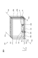
- FIG. 9 is a perspective view of the wireless communication device according to the third embodiment of the present invention.
- FIG. 10 shows a partially enlarged view of the wireless communication device according to the third embodiment of the present invention.
- FIG. 11 shows a schematic configuration of the wireless communication device according to the third embodiment.
- differences from the first embodiment will be mainly described.
- the same or equivalent components as those in the first embodiment will be described with the same reference numerals.
- descriptions overlapping with those in the first embodiment are omitted.
- the wireless communication device 10C is provided with a wiring pattern 40a and a through-hole plating 41 for forming a coil antenna on the circuit board 11a in advance as compared with the first embodiment. It is different in point.
- the third embodiment is also different from the first embodiment in that the element block 30a includes a plating nucleus material and that the LC resonance circuit is configured using the chip capacitors 15 and 16.
- the circuit board 11a has dimensions in the X-axis direction and Y-axis direction equal to the dimensions of the element block 30a, and constitutes the bottom of the wireless communication device 10C.
- the circuit board 11a is provided with a wiring pattern 40a connected to the interlayer conductors 20A and 20B on the second surface PS2.
- the wiring pattern 40a forms a part of the coil antenna and is formed of a plating pattern.
- the circuit board 11a is provided with through-hole plating 41 on the third surface PS3 and the fourth surface PS4 connected to the first surface PS1 and the second surface PS2.
- the through-hole plating 41 connects the wiring pattern 40a on the second surface PS2 of the circuit board 11a and the plating pattern 40b of the element block 30a. That is, as shown in FIG. 11, in the wireless communication device 10C, a coil antenna is formed by the wiring pattern 40a, the through-hole plating 41, and the plating pattern 40b.
- the chip capacitors 15 and 16 constitute a wireless IC element 12 and an LC resonance circuit and a matching circuit for adjusting the frequency.
- the chip capacitors 15 and 16 are used for coarse or fine adjustment of the frequency.
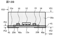
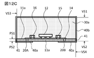
- FIGS. 12A to 12C are diagrams sequentially illustrating manufacturing steps of the wireless communication device 10C. Note that in the method for manufacturing the wireless communication device 10C according to the third embodiment, the description of the same parts as those in the first and second embodiments is omitted.
- a circuit board 11a is prepared.
- a wiring conductor pattern 14 is formed on the first surface PS1 side of the circuit board 11a, and the RFIC element 12 and the chip capacitors 15 and 16 are mounted on the wiring conductor pattern 14.
- a wiring pattern 40a connected to the interlayer conductors 20A and 20B is formed on the second surface PS2 side of the circuit board 11a.
- a through-hole plating 41 connected to the wiring pattern 40a is formed on the third surface PS3 and the fourth surface PS4 side of the circuit board 11a.
- the wiring pattern 40a is formed of, for example, a plating layer (plating pattern).
- the first surface PS1 side of the circuit board 11a is covered with the element block 30a.
- the element block 30a is formed, for example, by applying a liquid thermosetting resin to the first surface PS1 of the circuit board 11a and curing it by heat treatment.
- the element block 30a may be formed by covering and curing a semi-cured resin sheet on the first surface PS1 of the circuit board 11.
- the upper surface of the element block 30a is planarized by surface polishing.
- base_body block 30a may be chamfered. By chamfering the corner a of the element block 30, laser processing described later can be performed smoothly.
- a plating pattern 40b is formed on the element block 30a.
- the plating pattern 40b is connected to the through-hole plating 41 of the circuit board 11a.
- a coil antenna can be formed by the wiring pattern 40a of the circuit board 11a, the through-hole plating 41, and the plating pattern 40b of the element block 30a.
- the plating pattern 40b is formed using a processing technique such as LDS or MID, for example.
- the plating pattern 40b is formed using the LDS processing technique.
- a continuous plating film on the surface of the wiring pattern 40a and the through-hole conductor 41 and the plating pattern 40b of the circuit board 11a by further performing electrolytic plating.
- the connection reliability between the through-hole conductor 41 and the plating pattern 40b can be improved, and the DC resistance value of the coil antenna can be reduced.
- the wireless communication device 10C is manufactured by performing the steps shown in FIGS. 12A to 12C. Also, the wireless communication device 10C may be manufactured using a collective substrate, as in the first and second embodiments.
- the coil antenna can be easily formed using the LDS processing technique even when the circuit board 11a forms the bottom of the device.
- the time for forming the coil antenna can be shortened.
- the present invention is not limited to this.
- FIG. 13 is a perspective view of the wireless communication device according to the fourth embodiment of the present invention.
- FIG. 14 shows a schematic configuration of the wireless communication device according to the fourth embodiment.
- differences from the first embodiment will be mainly described.
- the same or equivalent components as those in the first embodiment will be described with the same reference numerals.
- descriptions overlapping with those in the first embodiment are omitted.
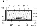
- the wireless communication device 10D has a thick film layer 60 containing plating nuclei coated on the outer peripheral surfaces of the circuit board 11b and the element block 30 as compared with the first embodiment. Is different.
- the fourth embodiment is also different from the first embodiment in that an antenna resonant circuit is configured using the chip capacitors 15 and 16.
- the circuit board 11b has dimensions in the X-axis direction and the Y-axis direction equal to the dimensions of the element block 30, and constitutes the bottom of the wireless communication device 10D.
- the outer surfaces of the circuit board 11b and the element block 30 are coated with a thick film layer 60 containing plating nuclei. More specifically, as shown in FIG. 14, the thick film layer 60 including the plating nucleus includes the second surface PS2 of the circuit board 11b, the first main surface VS1, the second main surface VS2, and the first surface of the element block 30.
- the side surface VS3 and the second side surface VS4 are coated.
- the wireless communication device 10D forms the plating pattern 40 in the pattern formation region by irradiating the thick film layer 60 including the plating nucleus coated on the outer periphery of the circuit board 11b and the element block 30 with a laser.
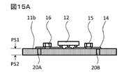
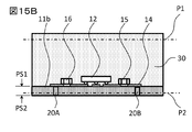
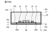
- FIGS. 15A to 15D are diagrams sequentially illustrating the manufacturing process of the wireless communication device 10D. Note that in the method for manufacturing the wireless communication device 10D according to the fourth embodiment, the description of the same parts as those in the first embodiment is omitted.
- a circuit board 11b is prepared.
- a wiring conductor pattern 14 is formed on the first surface PS1 side of the circuit board 11b, and the RFIC element 12 and the chip capacitors 15 and 16 are mounted on the wiring conductor pattern 14.
- Interlayer conductors 20A and 20B extending from the first surface PS1 to the second surface PS2 are provided inside the circuit board 11b.
- the first surface PS1 side of the circuit board 11b is covered with the element block 30.
- the upper surface of the element block 30 is flattened by surface polishing to a predetermined polishing position P1.
- the second surface PS2 of the circuit board 11b is subjected to surface polishing to a predetermined polishing position P2, thereby exposing the end portions of the interlayer conductors 20A and 20B.
- the corners of the element block 30 may be chamfered. By chamfering the corners of the element block 30, laser processing to be described later can be performed smoothly.
- the outer periphery of the circuit board 11b and the element block 30 is coated with a thick film layer 60 containing plating nuclei.
- the thick film layer 60 including the plating nucleus includes the second surface PS2 of the circuit board 11b, the first main surface VS1, the second main surface VS2, the first side surface VS3, and the second side surface VS4 of the element block 30. Coated.
- a coil antenna is formed by forming a plating pattern 40 by laser processing the thick film layer 60 containing plating nuclei.
- the plating pattern is formed using the LDS processing technique.
- the plating nucleus is exposed to the outer surface, and the plating film is grown from the exposed plating nucleus.
- the pattern formation region is a portion where the coil antenna, that is, the plating pattern 40 is to be formed. Thereafter, the plating pattern 40 is formed by thickening the plating film by performing electrolytic plating.
- the protective layer 50 may be formed on the surface of the circuit board 11a and the element block 30a.
- the wireless communication device 10D is manufactured by performing the steps shown in FIGS. 15A to 15D. Further, the wireless communication device 10D may be manufactured using a collective substrate, as in the first and second embodiments.
- the wireless communication device 10D according to Embodiment 4 can provide the following effects.
- the coil An antenna can be easily formed.
- a coil antenna can be formed at a lower cost compared to an element block including a plating core material.
- the thick film layer 60 including the plating nucleus only needs to be coated on the portion where the plating pattern 40 is formed.
- the thick film layer 60 including the plating nucleus may be partially coated on each surface of the element block 30.
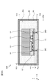
- FIG. 16 shows a schematic configuration of the wireless communication device according to the fifth embodiment.
- differences from the second embodiment will be mainly described.
- the same or equivalent components as those in the second embodiment will be described with the same reference numerals.
- descriptions overlapping with those in the second embodiment are omitted.
- the wireless communication device 10E according to the fifth embodiment is different from the second embodiment in that it includes a sealing resin layer 17 and a magnetic block 18.
- the sealing resin layer 17 is formed on the first surface PS ⁇ b> 1 side of the circuit board 11, and the magnetic block 18 is disposed on the sealing resin layer 17. .
- the circuit board 11, the sealing resin layer 17, and the magnetic block 18 are embedded in the element block 30 and disposed inside the coil antenna.
- the sealing resin layer 17 seals surface mounted components such as the RFIC 12 and the chip capacitor 13 mounted on the first surface PS1 of the circuit board 11.
- the sealing resin layer 17 is made of, for example, a thermosetting resin such as an epoxy resin.
- the magnetic body block 18 is disposed on the sealing resin layer 17.
- the magnetic body block 18 has a rectangular parallelepiped shape, and is made of, for example, ferrite.
- the magnetic block 18 is disposed inside the coil antenna and acts as a magnetic core (magnetic core) for the coil antenna.
- the wireless communication device 10E according to Embodiment 5 can provide the following effects.
- the surface-mounted component on the first surface PS1 side of the circuit board 11 is sealed with the sealing resin layer 17, and the magnetic block 18 is placed on the sealing resin layer 17. It is arranged.
- the magnetic body block 18 is arrange
- the surface mount component can be protected by sealing the surface mount component mounted on the first surface PS1 side of the circuit board 11 with the sealing resin layer 17. it can.
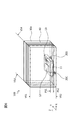
- FIG. 17 is a perspective view of article 100 with a wireless communication device according to the sixth embodiment.
- the article 100 with a wireless communication device is a resin molded body 101 with a built-in wireless communication device, for example, a toy such as a miniature car made by resin molding.
- the wireless communication device-equipped article 100 includes the wireless communication device 10A according to the first embodiment as a wireless communication device.
- the wireless communication device-equipped article 100 can be formed, for example, by injection molding a molding resin such as an epoxy resin in a state where the wireless communication device 10A is fixed in the mold for the resin molded product.
- the wireless communication device 10 ⁇ / b> A is embedded in the resin molded body 101 and is not exposed to the outside of the article 100.
- the wireless communication device 10A is embedded in the bottom of a toy.
- the bottom of the toy corresponds to the vicinity of the top surface of the RFID-tagged article 301 from the viewpoint of FIG.
- the winding axis of the coil antenna of the wireless communication device 10A faces the normal direction with respect to the bottom surface of a toy such as a miniature car. Therefore, the reader / writer device communicates with the wireless communication device 10A by making the bottom surface of the toy face the reading unit of the reader / writer device. Thus, the reader / writer device or the host device connected to the reader / writer device performs a predetermined process.
- the wireless communication device 10A in which the surface on which the surface mounting component is mounted on the circuit board 11 is covered with the element block 30 is used.
- a mounting component such as an RFIC element is sandwiched between the circuit board 11 and the element block 30, and it is wireless with respect to an injection molding resin that flows with high heat when the resin molding 101 is injection molded.
- the solder connection portion of the surface mount chip component in the communication device 10 ⁇ / b> A is protected by the element block 30. Therefore, according to the article 100 with the wireless communication device, excellent electrical characteristics and heat resistance that can be communicated by a reader / writer device or the like are high, and the reliability is high.
- Embodiment 6 although the article
- an article provided with the wireless communication device of Embodiments 2 to 5 may be used.
- the article 100 with the wireless communication device may be, for example, a container or tableware in which the wireless communication device 10A is embedded by resin molding. It is particularly suitable for articles that are exposed to high temperatures for disinfection and the like.
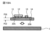
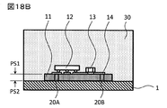
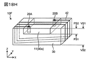
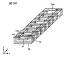
- FIGS. 18A to 18I are diagrams sequentially illustrating manufacturing steps of the wireless communication device 10F. Note that in the method for manufacturing the wireless communication device 10F according to the seventh embodiment, the description of the same parts as those in the first to sixth embodiments is omitted. 18A to 18I, the RFIC element 12 and the like mounted on the circuit board 11 are not shown for ease of explanation.
- the coil antenna is formed by winding metal wire 42 around element block 30 as compared with the first to fifth embodiments.
- the point of formation is different. That is, the wireless communication device 10F according to the seventh embodiment is different from the first to fifth embodiments in that the coil antenna is formed of the metal wire 42.
- a circuit board 11 is prepared in which an RFIC element 12 and a chip capacitor 13 are mounted on a wiring conductor pattern 14 provided on the first surface PS1 side, and interlayer conductors 20A and 20B are provided therein. To do.
- the circuit board 11 is arranged on the base 1 with the second surface PS2 side as a lower surface.
- An adhesive layer (not shown) is provided on the pedestal 1, and the second surface PS2 side of the circuit board 11 is in contact with the adhesive layer. That is, the circuit board 11 is fixed to the adhesive layer of the base 1.
- the circuit board 11 on the pedestal 1 is covered with the element block 30.
- the element block 30 is formed, for example, by applying a liquid thermosetting resin on the pedestal 1 on which the circuit board 11 is disposed, and curing it by heat treatment.
- the element block 30 may be formed by covering a circuit board 11 with a semi-cured resin sheet and curing it.
- the base 1 is removed, and the upper surface and the lower surface of the element block 30 are subjected to surface polishing.
- the element block 30 is polished to predetermined polishing positions P1 and P2 by, for example, buffing or scribing.
- the upper and lower surfaces of the element block 30 can be planarized as shown in FIG. 18D.
- wireless communication device 10F can also be adjusted by adjusting the predetermined grinding
- FIG. 18E shows the appearance of the resulting product created in the manufacturing process of FIG. 18D.
- the first main surface VS1 that is the lower surface of the element block 30 and the second surface PS2 of the circuit board 11 are formed on the same plane.
- the end surfaces of the interlayer conductors 20A and 20B are exposed on the second surface PS2 of the circuit board 11.
- one end of the metal wire 42 is attached to the end surface of the interlayer conductor 20A exposed on the second surface PS2 of the circuit board 11 by welding or the like.
- the metal wire 42 for example, a copper wire or the like can be used.
- the metal wire 42 is wound around the element block 30.
- a metal wire 42 circulates around the element block 30 around the Y-axis direction to form a rectangular helical coil antenna.
- the element block 30 may be formed with a groove in which at least a part of the metal wire 42 enters at a portion around which the metal wire 42 is wound.
- the metal wire 42 is wound around the element block 30 to form a coil antenna, and then the other end of the metal wire 42 is attached to the end face of the interlayer conductor 20B by welding or the like.
- the metal wire 42 is wound around the element block 30 in a three-turn rectangular helical shape, but is not limited thereto.
- the number of turns, the coil shape, and the like may be changed according to, for example, the shape of the wireless communication device 10F, that is, the shape of the element block 30 serving as the base substrate.
- FIG. 18I description is made using one circuit board 11 for ease of explanation, but in the seventh embodiment, as shown in FIG. 18I, a plurality of circuit boards 11 are arranged in a line.
- the wireless communication device 10F is manufactured using the mother substrate 90a provided continuously. Specifically, the mother substrate 90a fixed on the base 1 is covered with the element block 30 (see FIGS. 18A to 18B). Next, the upper and lower surfaces of the element block 30 are flattened (see FIGS. 18C to 18E). By winding metal wires 42 around the respective circuit boards 11 of the mother board 90a (see FIGS. 18F to 18H), coil antennas corresponding to the respective circuit boards 11 are formed around the element block 30 (see FIG. 18). 18I).
- the mother board 90a when used, as shown in FIG. 18I, a collective board in which a plurality of wireless communication devices 10F are connected in the winding axis direction, that is, the Y-axis direction is produced.
- the collective substrate After forming a protective layer on the outer periphery of the collective substrate, the collective substrate is cut in a direction intersecting the winding axis direction, that is, in the X-axis direction or the Z-axis direction in FIG. Is divided into pieces.
- the individual wireless communication device 10F is acquired from the collective substrate.
- the element block 30 for example, a resin block made of an epoxy resin or the like is used.
- the resin block preferably contains a magnetic filler such as ferrite powder or metal magnetic powder.
- a magnetic filler such as ferrite powder or metal magnetic powder.
- the wireless communication device 10F according to Embodiment 7 can provide the following effects.
- the resistance of the coil antenna itself can be reduced by forming the coil antenna with the metal wire 42 as compared with the case where the coil antenna is formed with the plating pattern. .
- the metal wire 42 straddles the circuit board 11 and the element block 30 and is wound around the element block 30. Therefore, the circuit board 11 is fixed to the element block 30 by the metal wire 42. be able to. Thereby, the metal wire 42 can prevent the circuit board 11 from falling off the element block 30.
- the metal wire 42 may be, for example, a metal wire (covered wire) covered with an insulating film.
- Embodiment 7 although the example which manufactures several radio
- the manufacturing method of the seventh embodiment may be used to manufacture one wireless communication device 10F.
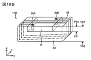
- FIGS. 19A and 19B are diagrams sequentially illustrating the manufacturing process of the wireless communication device 10G. Note that in the method for manufacturing the wireless communication device 10G according to the eighth embodiment, the description of the same parts as those in the first to seventh embodiments is omitted. 19 and 19B, illustration of the RFIC element 12 and the like mounted on the circuit board 11 is omitted for ease of explanation.
- the coil antenna is formed by attaching the spring material 43 to the element block 30 as compared with the seventh embodiment.
- the point is different. That is, the wireless communication device 10G according to the eighth embodiment is different from the seventh embodiment in that the coil antenna is formed of the spring material 43.
- the manufacturing method of the wireless communication device 10G according to the eighth embodiment is the same as the manufacturing method of the wireless communication device 10F according to the seventh embodiment shown in FIGS.
- a spring material 43 formed in a rectangular helical shape is attached to the element block 30 (see FIG. 18E) in which the circuit board 11 is embedded. Specifically, the spring member 43 is fitted into the element block 30 so that the element block 30 enters the inner region of the spring member 43.
- one end of the spring material 43 is welded to the end surface of the interlayer conductor 20A or connected using a conductive material such as solder. Further, the other end of the spring material 43 is welded to the end face of the interlayer conductor 20B, or is connected using a conductive material such as solder.
- the coil antenna is formed by the spring material 43 having spring properties.
- a plurality of wireless communication devices 10G may be manufactured using the mother substrate 90b.
- a groove into which the spring material 43 enters may be provided around the element block 30. Thereby, positioning of the spring material 43 can be performed easily.
- a resin block containing a magnetic filler such as ferrite powder or metal magnetic powder may be used as the element block 30.
- the wireless communication device 10G according to Embodiment 8 can provide the following effects.
- the wireless communication device 10G by forming the coil antenna with the spring material 43, the resistance of the coil antenna itself can be reduced as compared with the case where the coil antenna is formed with a plating pattern. .
- the spring material 43 is a metal having spring properties, the shape of the coil antenna can be maintained.
- the spring material 43 can be easily attached by deforming it.
- the spring member 43 returns to its original shape, so that the shape of the coil antenna can be maintained.
- the present invention is useful for a wireless communication device and can improve the connection reliability of a coil antenna.
Landscapes
- Engineering & Computer Science (AREA)
- Microelectronics & Electronic Packaging (AREA)
- Manufacturing & Machinery (AREA)
- Physics & Mathematics (AREA)
- General Physics & Mathematics (AREA)
- Theoretical Computer Science (AREA)
- Computer Hardware Design (AREA)
- Details Of Aerials (AREA)
Abstract
Afin d'augmenter la fiabilité de connexion dans des antennes à cadre, l'invention porte sur un procédé de fabrication de dispositifs de communication sans fil qui comprend : une étape à laquelle une carte de circuit imprimé est préparée qui comprend un élément à circuit intégré radiofréquence (RFIC) monté sur une première surface et un conducteur inter-couche connecté à l'élément RFIC et s'étendant de la première surface à une deuxième surface en regard de la première surface ; une étape à laquelle au moins la première surface de la carte de circuit imprimé est recouverte d'un bloc d'élément ; et une étape à laquelle un conducteur en forme de bobine entourant la carte de circuit imprimé et le bloc d'élément et connecté à une partie terminale du conducteur inter-couche est utilisé et une antenne à cadre connectée à l'élément RFIC par l'intermédiaire du conducteur inter-couche est formée.
Priority Applications (1)
| Application Number | Priority Date | Filing Date | Title |
|---|---|---|---|
| JP2017526613A JP6187728B1 (ja) | 2016-02-17 | 2017-01-27 | 無線通信デバイス、及びその製造方法 |
Applications Claiming Priority (2)
| Application Number | Priority Date | Filing Date | Title |
|---|---|---|---|
| JP2016-028171 | 2016-02-17 | ||
| JP2016028171 | 2016-02-17 |
Publications (1)
| Publication Number | Publication Date |
|---|---|
| WO2017141663A1 true WO2017141663A1 (fr) | 2017-08-24 |
Family
ID=59625028
Family Applications (1)
| Application Number | Title | Priority Date | Filing Date |
|---|---|---|---|
| PCT/JP2017/002888 Ceased WO2017141663A1 (fr) | 2016-02-17 | 2017-01-27 | Dispositif de communication sans fil et son procédé de fabrication |
Country Status (2)
| Country | Link |
|---|---|
| JP (1) | JP6187728B1 (fr) |
| WO (1) | WO2017141663A1 (fr) |
Cited By (5)
| Publication number | Priority date | Publication date | Assignee | Title |
|---|---|---|---|---|
| CN112599515A (zh) * | 2019-10-02 | 2021-04-02 | 安靠科技新加坡控股私人有限公司 | 半导体装置以及制造半导体装置的方法 |
| JP2021117004A (ja) * | 2020-01-22 | 2021-08-10 | 株式会社東芝 | チップパッケージ |
| JP2021145120A (ja) * | 2020-03-12 | 2021-09-24 | 住友ベークライト株式会社 | 電子装置 |
| WO2022074983A1 (fr) * | 2020-10-05 | 2022-04-14 | ローム株式会社 | Composant de circuit et dispositif à semi-conducteur |
| JPWO2024106370A1 (fr) * | 2022-11-14 | 2024-05-23 |
Citations (5)
| Publication number | Priority date | Publication date | Assignee | Title |
|---|---|---|---|---|
| JP2006333403A (ja) * | 2005-05-30 | 2006-12-07 | Hitachi Ltd | 無線icタグ、及び無線icタグの製造方法 |
| JP2007280343A (ja) * | 2006-02-10 | 2007-10-25 | Fujitsu Ltd | Rfidタグの製造方法およびrfidタグ |
| WO2010119854A1 (fr) * | 2009-04-14 | 2010-10-21 | 株式会社村田製作所 | Composant pour dispositif de ci sans fil et dispositif de ci sans fil |
| JP2011211748A (ja) * | 2008-02-27 | 2011-10-20 | Mitsubishi Electric Corp | Rfidタグ |
| JP5477459B2 (ja) * | 2010-03-12 | 2014-04-23 | 株式会社村田製作所 | 無線通信デバイス及び金属製物品 |
-
2017
- 2017-01-27 WO PCT/JP2017/002888 patent/WO2017141663A1/fr not_active Ceased
- 2017-01-27 JP JP2017526613A patent/JP6187728B1/ja active Active
Patent Citations (5)
| Publication number | Priority date | Publication date | Assignee | Title |
|---|---|---|---|---|
| JP2006333403A (ja) * | 2005-05-30 | 2006-12-07 | Hitachi Ltd | 無線icタグ、及び無線icタグの製造方法 |
| JP2007280343A (ja) * | 2006-02-10 | 2007-10-25 | Fujitsu Ltd | Rfidタグの製造方法およびrfidタグ |
| JP2011211748A (ja) * | 2008-02-27 | 2011-10-20 | Mitsubishi Electric Corp | Rfidタグ |
| WO2010119854A1 (fr) * | 2009-04-14 | 2010-10-21 | 株式会社村田製作所 | Composant pour dispositif de ci sans fil et dispositif de ci sans fil |
| JP5477459B2 (ja) * | 2010-03-12 | 2014-04-23 | 株式会社村田製作所 | 無線通信デバイス及び金属製物品 |
Cited By (11)
| Publication number | Priority date | Publication date | Assignee | Title |
|---|---|---|---|---|
| CN112599515A (zh) * | 2019-10-02 | 2021-04-02 | 安靠科技新加坡控股私人有限公司 | 半导体装置以及制造半导体装置的方法 |
| JP2021117004A (ja) * | 2020-01-22 | 2021-08-10 | 株式会社東芝 | チップパッケージ |
| JP7596070B2 (ja) | 2020-01-22 | 2024-12-09 | 株式会社東芝 | チップパッケージ |
| JP2021145120A (ja) * | 2020-03-12 | 2021-09-24 | 住友ベークライト株式会社 | 電子装置 |
| JP7562989B2 (ja) | 2020-03-12 | 2024-10-08 | 住友ベークライト株式会社 | 電子装置 |
| WO2022074983A1 (fr) * | 2020-10-05 | 2022-04-14 | ローム株式会社 | Composant de circuit et dispositif à semi-conducteur |
| JPWO2022074983A1 (fr) * | 2020-10-05 | 2022-04-14 | ||
| JP7747648B2 (ja) | 2020-10-05 | 2025-10-01 | ローム株式会社 | 回路部品および半導体装置 |
| JPWO2024106370A1 (fr) * | 2022-11-14 | 2024-05-23 | ||
| WO2024106370A1 (fr) * | 2022-11-14 | 2024-05-23 | 株式会社村田製作所 | Module rfid |
| JP7733359B2 (ja) | 2022-11-14 | 2025-09-03 | 株式会社村田製作所 | Rfidモジュール |
Also Published As
| Publication number | Publication date |
|---|---|
| JP6187728B1 (ja) | 2017-08-30 |
| JPWO2017141663A1 (ja) | 2018-02-22 |
Similar Documents
| Publication | Publication Date | Title |
|---|---|---|
| US10784929B2 (en) | Wireless IC device | |
| JP6187728B1 (ja) | 無線通信デバイス、及びその製造方法 | |
| US9490062B2 (en) | Chip electronic component | |
| JP6222319B2 (ja) | 無線icデバイス、それを備えた樹脂成型体、それを備えた通信端末装置 | |
| CN106373709B (zh) | 模块基板 | |
| US10122068B2 (en) | Wireless IC device, molded resin article, and method for manufacturing coil antenna | |
| JP6648830B2 (ja) | コイルモジュール | |
| JP6222398B2 (ja) | 無線icデバイス、それを備えた樹脂成型体、それを備えた通信端末装置、及びその製造方法 | |
| JP2010028351A (ja) | ブースターアンテナ及び非接触情報媒体 | |
| WO2017141771A1 (fr) | Dispositif de communication sans fil, procédé de production associé et corps moulé en résine | |
| JP6160796B1 (ja) | 無線通信デバイス及びその製造方法、並びに、樹脂成型体 | |
| WO2017141597A1 (fr) | Dispositif de communications sans fil, procédé pour sa production, et corps moulé en résine | |
| JP6135837B1 (ja) | 無線通信デバイス及びその製造方法、並びに、樹脂成型体 | |
| WO2017145505A1 (fr) | Dispositif à ci sans fil et procédé de fabrication de dispositif à ci sans fil |
Legal Events
| Date | Code | Title | Description |
|---|---|---|---|
| ENP | Entry into the national phase |
Ref document number: 2017526613 Country of ref document: JP Kind code of ref document: A |
|
| 121 | Ep: the epo has been informed by wipo that ep was designated in this application |
Ref document number: 17752926 Country of ref document: EP Kind code of ref document: A1 |
|
| NENP | Non-entry into the national phase |
Ref country code: DE |
|
| 122 | Ep: pct application non-entry in european phase |
Ref document number: 17752926 Country of ref document: EP Kind code of ref document: A1 |