WO2017145808A1 - Procédé de planarisation pour substrats semi-conducteurs au moyen d'une composition contenant du silicium - Google Patents
Procédé de planarisation pour substrats semi-conducteurs au moyen d'une composition contenant du silicium Download PDFInfo
- Publication number
- WO2017145808A1 WO2017145808A1 PCT/JP2017/004918 JP2017004918W WO2017145808A1 WO 2017145808 A1 WO2017145808 A1 WO 2017145808A1 JP 2017004918 W JP2017004918 W JP 2017004918W WO 2017145808 A1 WO2017145808 A1 WO 2017145808A1
- Authority
- WO
- WIPO (PCT)
- Prior art keywords
- group
- polysiloxane
- coating
- methyl
- mol
- Prior art date
- Legal status (The legal status is an assumption and is not a legal conclusion. Google has not performed a legal analysis and makes no representation as to the accuracy of the status listed.)
- Ceased
Links
Images


Classifications
-
- H—ELECTRICITY
- H10—SEMICONDUCTOR DEVICES; ELECTRIC SOLID-STATE DEVICES NOT OTHERWISE PROVIDED FOR
- H10P—GENERIC PROCESSES OR APPARATUS FOR THE MANUFACTURE OR TREATMENT OF DEVICES COVERED BY CLASS H10
- H10P76/00—Manufacture or treatment of masks on semiconductor bodies, e.g. by lithography or photolithography
- H10P76/20—Manufacture or treatment of masks on semiconductor bodies, e.g. by lithography or photolithography of masks comprising organic materials
- H10P76/204—Manufacture or treatment of masks on semiconductor bodies, e.g. by lithography or photolithography of masks comprising organic materials of organic photoresist masks
- H10P76/2041—Photolithographic processes
-
- C—CHEMISTRY; METALLURGY
- C09—DYES; PAINTS; POLISHES; NATURAL RESINS; ADHESIVES; COMPOSITIONS NOT OTHERWISE PROVIDED FOR; APPLICATIONS OF MATERIALS NOT OTHERWISE PROVIDED FOR
- C09D—COATING COMPOSITIONS, e.g. PAINTS, VARNISHES OR LACQUERS; FILLING PASTES; CHEMICAL PAINT OR INK REMOVERS; INKS; CORRECTING FLUIDS; WOODSTAINS; PASTES OR SOLIDS FOR COLOURING OR PRINTING; USE OF MATERIALS THEREFOR
- C09D183/00—Coating compositions based on macromolecular compounds obtained by reactions forming in the main chain of the macromolecule a linkage containing silicon, with or without sulfur, nitrogen, oxygen, or carbon only; Coating compositions based on derivatives of such polymers
- C09D183/04—Polysiloxanes
- C09D183/06—Polysiloxanes containing silicon bound to oxygen-containing groups
-
- B—PERFORMING OPERATIONS; TRANSPORTING
- B05—SPRAYING OR ATOMISING IN GENERAL; APPLYING FLUENT MATERIALS TO SURFACES, IN GENERAL
- B05D—PROCESSES FOR APPLYING FLUENT MATERIALS TO SURFACES, IN GENERAL
- B05D7/00—Processes, other than flocking, specially adapted for applying liquids or other fluent materials to particular surfaces or for applying particular liquids or other fluent materials
- B05D7/24—Processes, other than flocking, specially adapted for applying liquids or other fluent materials to particular surfaces or for applying particular liquids or other fluent materials for applying particular liquids or other fluent materials
-
- C—CHEMISTRY; METALLURGY
- C09—DYES; PAINTS; POLISHES; NATURAL RESINS; ADHESIVES; COMPOSITIONS NOT OTHERWISE PROVIDED FOR; APPLICATIONS OF MATERIALS NOT OTHERWISE PROVIDED FOR
- C09D—COATING COMPOSITIONS, e.g. PAINTS, VARNISHES OR LACQUERS; FILLING PASTES; CHEMICAL PAINT OR INK REMOVERS; INKS; CORRECTING FLUIDS; WOODSTAINS; PASTES OR SOLIDS FOR COLOURING OR PRINTING; USE OF MATERIALS THEREFOR
- C09D183/00—Coating compositions based on macromolecular compounds obtained by reactions forming in the main chain of the macromolecule a linkage containing silicon, with or without sulfur, nitrogen, oxygen, or carbon only; Coating compositions based on derivatives of such polymers
- C09D183/04—Polysiloxanes
- C09D183/08—Polysiloxanes containing silicon bound to organic groups containing atoms other than carbon, hydrogen, and oxygen
-
- G—PHYSICS
- G03—PHOTOGRAPHY; CINEMATOGRAPHY; ANALOGOUS TECHNIQUES USING WAVES OTHER THAN OPTICAL WAVES; ELECTROGRAPHY; HOLOGRAPHY
- G03F—PHOTOMECHANICAL PRODUCTION OF TEXTURED OR PATTERNED SURFACES, e.g. FOR PRINTING, FOR PROCESSING OF SEMICONDUCTOR DEVICES; MATERIALS THEREFOR; ORIGINALS THEREFOR; APPARATUS SPECIALLY ADAPTED THEREFOR
- G03F7/00—Photomechanical, e.g. photolithographic, production of textured or patterned surfaces, e.g. printing surfaces; Materials therefor, e.g. comprising photoresists; Apparatus specially adapted therefor
- G03F7/004—Photosensitive materials
- G03F7/09—Photosensitive materials characterised by structural details, e.g. supports, auxiliary layers
- G03F7/11—Photosensitive materials characterised by structural details, e.g. supports, auxiliary layers having cover layers or intermediate layers, e.g. subbing layers
-
- G—PHYSICS
- G03—PHOTOGRAPHY; CINEMATOGRAPHY; ANALOGOUS TECHNIQUES USING WAVES OTHER THAN OPTICAL WAVES; ELECTROGRAPHY; HOLOGRAPHY
- G03F—PHOTOMECHANICAL PRODUCTION OF TEXTURED OR PATTERNED SURFACES, e.g. FOR PRINTING, FOR PROCESSING OF SEMICONDUCTOR DEVICES; MATERIALS THEREFOR; ORIGINALS THEREFOR; APPARATUS SPECIALLY ADAPTED THEREFOR
- G03F7/00—Photomechanical, e.g. photolithographic, production of textured or patterned surfaces, e.g. printing surfaces; Materials therefor, e.g. comprising photoresists; Apparatus specially adapted therefor
- G03F7/16—Coating processes; Apparatus therefor
-
- G—PHYSICS
- G03—PHOTOGRAPHY; CINEMATOGRAPHY; ANALOGOUS TECHNIQUES USING WAVES OTHER THAN OPTICAL WAVES; ELECTROGRAPHY; HOLOGRAPHY
- G03F—PHOTOMECHANICAL PRODUCTION OF TEXTURED OR PATTERNED SURFACES, e.g. FOR PRINTING, FOR PROCESSING OF SEMICONDUCTOR DEVICES; MATERIALS THEREFOR; ORIGINALS THEREFOR; APPARATUS SPECIALLY ADAPTED THEREFOR
- G03F7/00—Photomechanical, e.g. photolithographic, production of textured or patterned surfaces, e.g. printing surfaces; Materials therefor, e.g. comprising photoresists; Apparatus specially adapted therefor
- G03F7/26—Processing photosensitive materials; Apparatus therefor
- G03F7/38—Treatment before imagewise removal, e.g. prebaking
-
- H—ELECTRICITY
- H10—SEMICONDUCTOR DEVICES; ELECTRIC SOLID-STATE DEVICES NOT OTHERWISE PROVIDED FOR
- H10P—GENERIC PROCESSES OR APPARATUS FOR THE MANUFACTURE OR TREATMENT OF DEVICES COVERED BY CLASS H10
- H10P14/00—Formation of materials, e.g. in the shape of layers or pillars
- H10P14/60—Formation of materials, e.g. in the shape of layers or pillars of insulating materials
- H10P14/63—Formation of materials, e.g. in the shape of layers or pillars of insulating materials characterised by the formation processes
- H10P14/6326—Deposition processes
- H10P14/6342—Liquid deposition, e.g. spin-coating, sol-gel techniques or spray coating
-
- H—ELECTRICITY
- H10—SEMICONDUCTOR DEVICES; ELECTRIC SOLID-STATE DEVICES NOT OTHERWISE PROVIDED FOR
- H10P—GENERIC PROCESSES OR APPARATUS FOR THE MANUFACTURE OR TREATMENT OF DEVICES COVERED BY CLASS H10
- H10P14/00—Formation of materials, e.g. in the shape of layers or pillars
- H10P14/60—Formation of materials, e.g. in the shape of layers or pillars of insulating materials
- H10P14/66—Formation of materials, e.g. in the shape of layers or pillars of insulating materials characterised by the type of materials
- H10P14/668—Formation of materials, e.g. in the shape of layers or pillars of insulating materials characterised by the type of materials the materials being characterised by the deposition precursor materials
- H10P14/6681—Formation of materials, e.g. in the shape of layers or pillars of insulating materials characterised by the type of materials the materials being characterised by the deposition precursor materials the precursor containing a compound comprising Si
- H10P14/6682—Formation of materials, e.g. in the shape of layers or pillars of insulating materials characterised by the type of materials the materials being characterised by the deposition precursor materials the precursor containing a compound comprising Si the compound being a silane, e.g. disilane, methylsilane or chlorosilane
-
- H—ELECTRICITY
- H10—SEMICONDUCTOR DEVICES; ELECTRIC SOLID-STATE DEVICES NOT OTHERWISE PROVIDED FOR
- H10P—GENERIC PROCESSES OR APPARATUS FOR THE MANUFACTURE OR TREATMENT OF DEVICES COVERED BY CLASS H10
- H10P14/00—Formation of materials, e.g. in the shape of layers or pillars
- H10P14/60—Formation of materials, e.g. in the shape of layers or pillars of insulating materials
- H10P14/69—Inorganic materials
- H10P14/692—Inorganic materials composed of oxides, glassy oxides or oxide-based glasses
- H10P14/6921—Inorganic materials composed of oxides, glassy oxides or oxide-based glasses containing silicon
- H10P14/6922—Inorganic materials composed of oxides, glassy oxides or oxide-based glasses containing silicon the material containing Si, O and at least one of H, N, C, F or other non-metal elements, e.g. SiOC, SiOC:H or SiONC
-
- H—ELECTRICITY
- H10—SEMICONDUCTOR DEVICES; ELECTRIC SOLID-STATE DEVICES NOT OTHERWISE PROVIDED FOR
- H10P—GENERIC PROCESSES OR APPARATUS FOR THE MANUFACTURE OR TREATMENT OF DEVICES COVERED BY CLASS H10
- H10P76/00—Manufacture or treatment of masks on semiconductor bodies, e.g. by lithography or photolithography
- H10P76/40—Manufacture or treatment of masks on semiconductor bodies, e.g. by lithography or photolithography of masks comprising inorganic materials
- H10P76/405—Manufacture or treatment of masks on semiconductor bodies, e.g. by lithography or photolithography of masks comprising inorganic materials characterised by their composition, e.g. multilayer masks
-
- H—ELECTRICITY
- H10—SEMICONDUCTOR DEVICES; ELECTRIC SOLID-STATE DEVICES NOT OTHERWISE PROVIDED FOR
- H10P—GENERIC PROCESSES OR APPARATUS FOR THE MANUFACTURE OR TREATMENT OF DEVICES COVERED BY CLASS H10
- H10P76/00—Manufacture or treatment of masks on semiconductor bodies, e.g. by lithography or photolithography
- H10P76/40—Manufacture or treatment of masks on semiconductor bodies, e.g. by lithography or photolithography of masks comprising inorganic materials
- H10P76/408—Manufacture or treatment of masks on semiconductor bodies, e.g. by lithography or photolithography of masks comprising inorganic materials characterised by their sizes, orientations, dispositions, behaviours or shapes
- H10P76/4085—Manufacture or treatment of masks on semiconductor bodies, e.g. by lithography or photolithography of masks comprising inorganic materials characterised by their sizes, orientations, dispositions, behaviours or shapes characterised by the processes involved to create the masks
-
- H—ELECTRICITY
- H10—SEMICONDUCTOR DEVICES; ELECTRIC SOLID-STATE DEVICES NOT OTHERWISE PROVIDED FOR
- H10P—GENERIC PROCESSES OR APPARATUS FOR THE MANUFACTURE OR TREATMENT OF DEVICES COVERED BY CLASS H10
- H10P95/00—Generic processes or apparatus for manufacture or treatments not covered by the other groups of this subclass
- H10P95/06—Planarisation of inorganic insulating materials
- H10P95/062—Planarisation of inorganic insulating materials involving a dielectric removal step
- H10P95/064—Planarisation of inorganic insulating materials involving a dielectric removal step the removal being chemical etching
-
- C—CHEMISTRY; METALLURGY
- C08—ORGANIC MACROMOLECULAR COMPOUNDS; THEIR PREPARATION OR CHEMICAL WORKING-UP; COMPOSITIONS BASED THEREON
- C08G—MACROMOLECULAR COMPOUNDS OBTAINED OTHERWISE THAN BY REACTIONS ONLY INVOLVING UNSATURATED CARBON-TO-CARBON BONDS
- C08G77/00—Macromolecular compounds obtained by reactions forming a linkage containing silicon with or without sulfur, nitrogen, oxygen or carbon in the main chain of the macromolecule
- C08G77/04—Polysiloxanes
- C08G77/12—Polysiloxanes containing silicon bound to hydrogen
-
- C—CHEMISTRY; METALLURGY
- C08—ORGANIC MACROMOLECULAR COMPOUNDS; THEIR PREPARATION OR CHEMICAL WORKING-UP; COMPOSITIONS BASED THEREON
- C08G—MACROMOLECULAR COMPOUNDS OBTAINED OTHERWISE THAN BY REACTIONS ONLY INVOLVING UNSATURATED CARBON-TO-CARBON BONDS
- C08G77/00—Macromolecular compounds obtained by reactions forming a linkage containing silicon with or without sulfur, nitrogen, oxygen or carbon in the main chain of the macromolecule
- C08G77/04—Polysiloxanes
- C08G77/14—Polysiloxanes containing silicon bound to oxygen-containing groups
- C08G77/16—Polysiloxanes containing silicon bound to oxygen-containing groups to hydroxyl groups
-
- C—CHEMISTRY; METALLURGY
- C08—ORGANIC MACROMOLECULAR COMPOUNDS; THEIR PREPARATION OR CHEMICAL WORKING-UP; COMPOSITIONS BASED THEREON
- C08G—MACROMOLECULAR COMPOUNDS OBTAINED OTHERWISE THAN BY REACTIONS ONLY INVOLVING UNSATURATED CARBON-TO-CARBON BONDS
- C08G77/00—Macromolecular compounds obtained by reactions forming a linkage containing silicon with or without sulfur, nitrogen, oxygen or carbon in the main chain of the macromolecule
- C08G77/04—Polysiloxanes
- C08G77/14—Polysiloxanes containing silicon bound to oxygen-containing groups
- C08G77/18—Polysiloxanes containing silicon bound to oxygen-containing groups to alkoxy or aryloxy groups
-
- C—CHEMISTRY; METALLURGY
- C08—ORGANIC MACROMOLECULAR COMPOUNDS; THEIR PREPARATION OR CHEMICAL WORKING-UP; COMPOSITIONS BASED THEREON
- C08G—MACROMOLECULAR COMPOUNDS OBTAINED OTHERWISE THAN BY REACTIONS ONLY INVOLVING UNSATURATED CARBON-TO-CARBON BONDS
- C08G77/00—Macromolecular compounds obtained by reactions forming a linkage containing silicon with or without sulfur, nitrogen, oxygen or carbon in the main chain of the macromolecule
- C08G77/04—Polysiloxanes
- C08G77/22—Polysiloxanes containing silicon bound to organic groups containing atoms other than carbon, hydrogen and oxygen
- C08G77/28—Polysiloxanes containing silicon bound to organic groups containing atoms other than carbon, hydrogen and oxygen sulfur-containing groups
-
- C—CHEMISTRY; METALLURGY
- C08—ORGANIC MACROMOLECULAR COMPOUNDS; THEIR PREPARATION OR CHEMICAL WORKING-UP; COMPOSITIONS BASED THEREON
- C08G—MACROMOLECULAR COMPOUNDS OBTAINED OTHERWISE THAN BY REACTIONS ONLY INVOLVING UNSATURATED CARBON-TO-CARBON BONDS
- C08G77/00—Macromolecular compounds obtained by reactions forming a linkage containing silicon with or without sulfur, nitrogen, oxygen or carbon in the main chain of the macromolecule
- C08G77/48—Macromolecular compounds obtained by reactions forming a linkage containing silicon with or without sulfur, nitrogen, oxygen or carbon in the main chain of the macromolecule in which at least two but not all the silicon atoms are connected by linkages other than oxygen atoms
- C08G77/50—Macromolecular compounds obtained by reactions forming a linkage containing silicon with or without sulfur, nitrogen, oxygen or carbon in the main chain of the macromolecule in which at least two but not all the silicon atoms are connected by linkages other than oxygen atoms by carbon linkages
Definitions
- the present invention relates to a method for flatly coating a semiconductor substrate using a silicon-containing composition. More specifically, the present invention is particularly suitable for forming a flat film having a good coverage with respect to a resist pattern formed on a substrate to be processed and having a difference in height and density of the resist pattern. Regarding the method.
- a technique for forming a fine pattern on a substrate and etching the substrate in accordance with this pattern to process the substrate is widely used in the field of semiconductor manufacturing.
- a pattern inversion method as one of the pattern forming techniques.
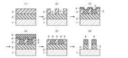
- a resist pattern is formed on the semiconductor substrate, and the resist pattern is covered with a silicon coating solution.
- the silicon-based coating liquid is filled between the resist patterns, and then baked to form a coating film.
- the upper part of the silicon-containing coating is etched back with a fluorine-based gas to expose the upper part of the resist pattern, and the gas is changed to remove the resist pattern with an oxygen-based etching gas.
- a silicon-based pattern derived from the film remains and the pattern is inverted.
- the reverse pattern is transferred to form a pattern on the substrate.
- a material using a polysiloxane and an ether solvent obtained by cohydrolysis of a silane having a group or an aryl group and tetraethoxysilane see Patent Document 1.
- the present invention uses a specific silicon-containing composition that can be satisfactorily embedded between resist patterns with respect to a stepped substrate having a difference in height or density in a resist pattern formed on a substrate to be processed, and steps according to a specific procedure.
- a method for flatly coating a substrate is provided.
- the present invention includes the following. [1] A first step of forming a first polysiloxane coating film by applying and baking a first coating polysiloxane composition containing a first coating polysiloxane on a stepped substrate, and further a first polysiloxane coating.
- a second step of forming a second polysiloxane coating film by applying and baking a second coating polysiloxane composition containing a second coating polysiloxane different from the first coating polysiloxane on the coating film A process for producing a polysiloxane-coated substrate manufactured through The iso-dense bias of the second polysiloxane coating film is 50 nm or less, Hydrolysis condensation of a hydrolyzable silane raw material containing the first hydrolyzable silane having 4 hydrolyzable groups per molecule in a proportion of 0 to 100 mol% in all silanes.
- the first coating polysiloxane is Formula (1): (In Formula (1), R 1 represents an alkyl group, an aryl group, a halogenated alkyl group, a halogenated aryl group, an alkoxyaryl group, an alkenyl group, or an epoxy group, an acryloyl group, a methacryloyl group, a mercapto group, or a cyano group.
- R 2 represents an alkoxy group, an acyloxy group, or a halogen group
- a represents an integer of 0 to 2.
- the second coating polysiloxane has the formula (1): (In Formula (1), R 1 represents an alkyl group, an aryl group, a halogenated alkyl group, a halogenated aryl group, an alkoxyaryl group, an alkenyl group, or an epoxy group, an acryloyl group, a methacryloyl group, a mercapto group, or a cyano
- a hydrolyzable silane represented by R 2 is an alkoxy group, an acyloxy group, or a halogen group, and a is 1.
- the second coating polysiloxane is 100 to 50 mol%, preferably 95 to 50 mol% of a hydrolyzable silane represented by the above formula (1) and a being 1;
- the hydrolyzable silane represented by the above formula (1) and a being 2 is 0 to 50 mol%, preferably 5 to 50 mol%.
- the second coating polysiloxane is a modified polysiloxane capped with a silanol group of a polysiloxane obtained by hydrolyzing and condensing a hydrolyzable silane raw material, the modified polysiloxane having a silanol group with respect to an Si atom.
- the modified polysiloxane has the formula (1): (In Formula (1), R 1 represents an alkyl group, an aryl group, a halogenated alkyl group, a halogenated aryl group, an alkoxyaryl group, an alkenyl group, or an epoxy group, an acryloyl group, a methacryloyl group, a mercapto group, or a cyano group. R 2 represents an alkoxy group, an acyloxy group, or a halogen group, and a is 0 to 100 mol of hydrolyzable silane.
- a method of planarizing a polysiloxane film on a stepped substrate [7] A first step of forming a first polysiloxane coating film by applying and baking a first coating polysiloxane composition containing a first coating polysiloxane on an organic pattern substrate, and further for the first coating A second polysiloxane coating film is formed by applying and baking a second coating polysiloxane composition on a first polysiloxane coating film containing a second coating polysiloxane different from the polysiloxane.
- a method for manufacturing a semiconductor device comprising: a step of etching back a polysiloxane-coated substrate manufactured through the steps to expose an organic pattern; and a step of etching and removing the organic pattern to invert the pattern.
- the coating polysiloxane composition of the present invention is coated on the patterned organic underlayer film without mixing with the patterned organic underlayer film formed on the substrate to be processed. It is possible to embed (fill) well between the patterns. In the present invention, by using a specific low silanol / low viscosity material, it becomes possible to embed a flat pattern without any difference in film thickness in various patterns.
- the coating polysiloxane composition is cured to form a polysiloxane composition film, and a flat surface can be formed later by etching back by etching (gas etching).
- the organic underlayer film can be removed by ashing (ashing treatment)
- the pattern of the organic underlayer film can be reversed to the pattern of the polysiloxane composition film formed by filling the coating polysiloxane composition.
- the substrate to be processed can be processed by these reversal patterns.
- the pattern can be reversed using a stepped substrate having a larger aspect ratio than the photoresist pattern on the substrate to be processed, and as a result, a reversed pattern having a high aspect ratio can be obtained.
- an organic underlayer film having a large aspect ratio can be embedded between patterns, coating with a specific polysiloxane composition is effective.
- a method of embedding (filling) a polysiloxane composition between photoresist patterns is difficult to perform ashing or the like because an organic film exists in the lower layer, and may be performed by gas etching. Many.
- the organic underlayer film on the substrate to be processed or on the oxide film can be reversed with the polysiloxane composition, it is cured after embedding the polysiloxane composition. The pattern can be easily reversed by the ashing process.
- the step can be completely flattened, and the super flatness of the coating film can be realized.
- a high etch resistance material for the first application not only the flatness of the coating film can be improved, but also high etching resistance can be realized.
- flattening is a coated coating in which a portion where a resist pattern exists (line portion) and a portion where a pattern does not exist (space portion) are present on the top when applied to a resist pattern. This means that there is little difference in film thickness.
- step difference board said to this invention, the wafer for semiconductor devices or a MEMS device is mentioned, for example.
- the semiconductor device manufacturing method including the method for planarizing a semiconductor substrate of the present invention usually includes a step (1) of applying a resist on the substrate, a step (2) of exposing and developing the resist, and a resist pattern during or after development.
- the step (3) is performed on the stepped substrate, The first step of applying and baking the first coating polysiloxane composition containing the first coating polysiloxane to form the first polysiloxane coating film, and the first polysiloxane coating film on the first polysiloxane coating film, A second step of forming a second polysiloxane coating film by applying and baking a second coating polysiloxane composition containing a second coating polysiloxane different from the coating polysiloxane Than is.
- the composition is coated on a resist pattern having a rough and dense
- the photoresist used in the step (1) is not particularly limited as long as it is sensitive to light used for exposure. Either a negative photoresist or a positive photoresist can be used.
- a positive photoresist comprising a novolac resin and 1,2-naphthoquinonediazide sulfonic acid ester, a chemically amplified photoresist comprising a binder having a group that decomposes with an acid to increase the alkali dissolution rate and a photoacid generator, an acid
- a chemically amplified photoresist comprising a low-molecular compound that decomposes to increase the alkali dissolution rate of the photoresist, an alkali-soluble binder, and a photoacid generator, and a binder having a group that decomposes with an acid to increase the alkali dissolution rate
- Examples include trade name APEX-E manufactured by Shipley, trade name PAR710 manufactured by Sumitomo Chemical Co., Ltd., and trade name SEPR430 manufactured by Shin-Etsu Chemical Co., Ltd. Also, for example, Proc. SPIE, Vol. 3999, 330-334 (2000), Proc. SPIE, Vol. 3999, 357-364 (2000), Proc. SPIE, Vol. 3999, 365-374 (2000), and fluorine-containing polymer-based photoresists.
- Chemically amplified resist comprising a binder having a group that decomposes with an acid generator and an acid to change the alkali dissolution rate, a low molecular weight compound that decomposes with an alkali-soluble binder, an acid generator and an acid to change the alkali dissolution rate of the resist
- a chemically amplified resist comprising: a binder having a group that decomposes with an acid generator and an acid to change the alkali dissolution rate; and a chemically amplified resist comprising a low-molecular compound that decomposes with an acid to change the alkali dissolution rate of the resist,
- non-chemically amplified resists composed of a binder having a group that changes the alkali dissolution rate by being decomposed by an electron beam and non-chemically amplified resists composed of a binder having a portion that is cut by an electron beam to change the alkali dis
- the resist solution is applied and then subjected to a baking temperature of 70 to 150 ° C. and a baking time of 0.5 to 5 minutes.
- the resist film thickness is obtained in the range of 10 to 1000 nm.
- the resist solution, the developer, and the coating materials shown below can be coated by spin coating, dipping, spraying, or the like, but the spin coating method is particularly preferable.
- the resist is exposed through a predetermined mask.
- a KrF excimer laser (wavelength 248 nm), an ArF excimer laser (wavelength 193 nm), EUV light (wavelength 13.5 nm), an electron beam, or the like can be used.
- post-exposure heating PEB: Post Exposure Bake
- the post-exposure heating is appropriately selected from a heating temperature of 70 ° C. to 150 ° C. and a heating time of 0.3 to 10 minutes.
- a step (1-1) of forming a resist underlayer film on the substrate can be included.
- the resist underlayer film has antireflection and organic hard mask functions.
- the formation of the resist in the step (1) can be performed by a step (1-1) in which a resist underlayer film is formed on the semiconductor substrate and a resist is formed thereon.
- a resist underlayer film is formed on a semiconductor substrate, a silicon hard mask is formed thereon, and a resist can be formed thereon.
- the resist underlayer film used in the above step (1-1) is for preventing irregular reflection during exposure of the upper layer resist, and is used for the purpose of improving adhesion with the resist.
- an acrylic resin or the like A novolac resin can be used.
- the resist underlayer film can form a film having a thickness of 1 to 1,000 nm on the semiconductor substrate.
- the resist underlayer film used in the above step (1-1) is a hard mask using an organic resin, and a material having a high carbon content and a low hydrogen content is used.
- a material having a high carbon content and a low hydrogen content is used.
- polyvinyl naphthalene resin, carbazole novolak resin, phenol novolak resin, naphthol novolak resin, and the like can be given. These can form a film with a film thickness of 5 to 1,000 nm on a semiconductor substrate.
- As the silicon hard mask used in the above step (1-1) polysiloxane obtained by hydrolyzing hydrolyzable silane can be used.
- polysiloxane obtained by hydrolyzing tetraethoxysilane, methyltrimethoxysilane, and phenyltriethoxysilane can be exemplified. These can form a film with a film thickness of 5 to 200 nm on the resist underlayer film.
- Step (2) exposure is performed through a predetermined mask.
- a KrF excimer laser (wavelength 248 nm), an ArF excimer laser (wavelength 193 nm), EUV (wavelength 13.5 nm), or the like can be used.
- post-exposure bake can be performed as necessary.
- the post-exposure heating is performed under conditions appropriately selected from a heating temperature of 70 ° C. to 150 ° C. and a heating time of 0.3 to 10 minutes.
- development is performed with a developer.
- a developer for example, when a positive photoresist is used, the exposed portion of the photoresist is removed, and a photoresist pattern is formed.
- Developers include aqueous solutions of alkali metal hydroxides such as potassium hydroxide and sodium hydroxide, aqueous solutions of quaternary ammonium hydroxides such as tetramethylammonium hydroxide, tetraethylammonium hydroxide and choline, ethanolamine, propylamine, An alkaline aqueous solution such as an aqueous amine solution such as ethylenediamine can be mentioned as an example. Further, a surfactant or the like can be added to these developers.
- the development conditions are appropriately selected from a temperature of 5 to 50 ° C. and a time of 10 to 600 seconds.
- an organic solvent can be used as the developer.
- development is performed with a developer (solvent). As a result, for example, when a positive photoresist is used, the unexposed portion of the photoresist is removed, and a photoresist pattern is formed.
- Developers include, for example, methyl acetate, butyl acetate, ethyl acetate, isopropyl acetate, amyl acetate, isoamyl acetate, ethyl methoxyacetate, ethyl ethoxy acetate, propylene glycol monomethyl ether acetate, ethylene glycol monoethyl ether acetate, ethylene glycol monopropyl Ether acetate, ethylene glycol monobutyl ether acetate, ethylene glycol monophenyl ether acetate, diethylene glycol monomethyl ether acetate, diethylene glycol monopropyl ether acetate, diethylene glycol monoethyl ether acetate, diethylene glycol monophenyl ether acetate, diethylene glycol monobutyl ether acetate, diethylene glycol Monoethyl ether acetate, 2-methoxybutyl acetate, 3-methoxybutyl acetate,
- a first polysiloxane coating film is prepared by applying and baking a first coating polysiloxane composition containing a first coating polysiloxane to a resist during or after development.
- a second coating polysiloxane composition containing a second coating polysiloxane different from the first coating polysiloxane is applied and baked to produce a second polysiloxane coating film.
- a polysiloxane composition film is formed in which the resist pattern is filled with the composition.
- the applied coating polysiloxane composition is fired at a heating temperature of 50 to 180 ° C. for 0.5 to 5 minutes, respectively.
- the iso-dense bias of the second polysiloxane coating film is 50 nm or less.
- the iso-dense bias of the second polysiloxane coating film is a portion having the smallest length from the interface on the side in contact with the film of the stepped substrate to the interface on the side of the second polysiloxane coating film in contact with the air. And the difference in film thickness from the largest part.
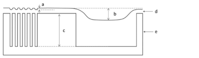
- the length b shown in FIG. 15 is the Iso-dense bias.
- a is the recess depth of the polysiloxane coating film at the center of the dense space portion
- b is the recess depth of the polysiloxane coating film at the center of the open space portion
- c is used.
- the depth of the initial space in the step substrate, d is a polysiloxane coating film, and e is the step substrate.
- the stepped substrate can be an organic pattern (photoresist pattern, resist underlayer film (coating type, vapor deposition type) pattern functioning as an etching mask for the lower semiconductor substrate, a pattern formed by nanoimprinting, etc.).
- a step (3-1) of exposing the surface of the resist pattern (for example, an organic pattern) by etching back the coating film surface can be included.
- the resist pattern surface and the coating composition surface coincide with each other, and only the resist component is removed from the difference in the gas etching rate between the resist pattern and the coating composition. Will remain, resulting in pattern inversion.
- the resist pattern is exposed by a gas (for example, a fluorine-based gas) that can remove the coating composition.
- step (4) the resist pattern is removed by etching to reverse the pattern.
- dry etching is performed using tetrafluoromethane, perfluorocyclobutane (C 4 F 8 ), perfluoropropane (C 3 F 8 ), trifluoromethane, carbon monoxide, argon, oxygen, nitrogen, sulfur hexafluoride. , Gas such as difluoromethane, nitrogen trifluoride and chlorine trifluoride.
- dry etching is preferably performed with an oxygen-based gas.
- a reverse pattern (reversal pattern) is formed by the polymer for pattern reversal formation (polysiloxane obtained by hydrolyzing and condensing hydrolyzable silane) contained in the coating composition.
- First coating polysiloxane composition comprising first coating polysiloxane
- First coating polysiloxane composition comprising first coating polysiloxane used in the first step of the method for producing a polysiloxane coated substrate according to the present invention Is described below.
- the first coating polysiloxane composition containing the first coating polysiloxane is applied on the patterned organic underlayer film, and at that time, partially on the upper surface of the organic underlayer film
- the silicon hard mask may remain. This is because the polysiloxane composition for the first coating later exposes the upper surface of the organic underlayer film by etchback, so that the polysiloxane for coating and the silicon hard mask are simultaneously removed by etchback.
- the polysiloxane for the first coating usually contains a hydrolysis condensate of a hydrolyzable silane raw material.
- the hydrolyzable silane raw material can contain one or more silanes.
- This hydrolyzable silane is a hydrolyzable condensate of a hydrolyzable silane raw material containing a first hydrolyzable silane having 4 hydrolyzable groups per molecule in a ratio of 0 to 100 mol% in all silanes. More preferably, the proportion of the first hydrolyzable silane having 4 hydrolyzable groups per molecule in the total silane is 0 to 50 mol%, and the total silane has 3 or 2 hydrolysates per molecule.
- a hydrolyzable condensate of a hydrolyzable silane raw material containing the first hydrolyzable silane having a decomposable group in a ratio of 50 (over) to 100 mol% is included.
- the hydrolyzable silane has the formula (1): (In Formula (1), R 1 represents an alkyl group, an aryl group, a halogenated alkyl group, a halogenated aryl group, an alkoxyaryl group, an alkenyl group, or an epoxy group, an acryloyl group, a methacryloyl group, a mercapto group, or a cyano group. And an organic group having an Si—C bond to a silicon atom, R 2 represents an alkoxy group, an acyloxy group, or a halogen group, and a represents an integer of 0 to 2. .
- hydrolyzable silane raw material 0 to 50 mol% of hydrolyzable silane in which a is 0 in formula (1) and a is 1 or 2 in formula (1) in all silanes.
- a certain hydrolyzable silane is contained in a proportion of 50 (over) to 100 mol%.
- the polysiloxane composition for the first coating of the present invention includes a hydrolysis condensate of a hydrolyzable silane raw material as represented by the above formula (1) and a solvent.
- a hydrolysis condensate of a hydrolyzable silane raw material as represented by the above formula (1)
- a solvent for example, acid, water, alcohol, curing catalyst, acid generator, other organic polymer, light-absorbing compound, surfactant and the like can be included.
- the solid content in the first coating polysiloxane composition of the present invention is, for example, 0.1 to 50% by mass, 0.1 to 30% by mass, 0.1 to 25% by mass, 0.5 to 20.0% by mass. Or 1.0 to 10.0% by mass.
- the solid content is obtained by removing the solvent component from all components of the first coating polysiloxane composition.
- the proportion of the hydrolyzable silane, its hydrolyzate, and its hydrolysis condensate in the solid content is 20% by mass or more, for example, 50 to 100% by mass, 60 to 99% by mass, 70 to 99% by mass. It is.
- the concentration of the hydrolyzable silane, its hydrolyzate, and its hydrolysis condensate (polysiloxane) in the composition is 0.5 to 20.0% by mass.
- the coating composition since the coating composition is used after exposure of the resist, the resist is exposed through a mask and filled with the composition during or after development.
- the hydrolyzable silane, its hydrolyzate, and its hydrolysis condensate have a resin component different from that of the resist.
- a new pattern is formed by the hydrolyzed condensate (polysiloxane) filled by selectively removing the resist by dry etching by selecting the gas type.
- hydrolyzable silane, its hydrolyzate, and its hydrolysis condensate can also be used as a mixture thereof. It can be used as a condensate obtained by hydrolyzing a hydrolyzable silane and condensing the obtained hydrolyzate.
- a hydrolysis-condensation product a partial hydrolysis product or a silane compound in which hydrolysis is not completely completed are mixed with the hydrolysis-condensation product, and the mixture can also be used.
- This condensate is a polymer having a polysiloxane structure.
- alkyl group examples include straight-chain or branched alkyl groups having 1 to 10 carbon atoms, such as methyl group, ethyl group, n-propyl group, i-propyl group, n-butyl group, i- Butyl, s-butyl, t-butyl, n-pentyl, 1-methyl-n-butyl, 2-methyl-n-butyl, 3-methyl-n-butyl, 1,1-dimethyl -N-propyl group, 1,2-dimethyl-n-propyl group, 2,2-dimethyl-n-propyl group, 1-ethyl-n-propyl group, n-hexyl, 1-methyl-n-pentyl group, 2-methyl-n-pentyl group, 3-methyl-n-pentyl group, 4-methyl-n-pentyl group, 1,1-dimethyl-n-butyl group, 1,2-dimethyl-n-butyl group, 1,2-
- Cyclic alkyl groups can also be used.
- examples of the cyclic alkyl group having 1 to 10 carbon atoms include cyclopropyl group, cyclobutyl group, 1-methyl-cyclopropyl group, 2-methyl-cyclopropyl group, cyclopentyl group, 1 -Methyl-cyclobutyl group, 2-methyl-cyclobutyl group, 3-methyl-cyclobutyl group, 1,2-dimethyl-cyclopropyl group, 2,3-dimethyl-cyclopropyl group, 1-ethyl-cyclopropyl group, 2- Ethyl-cyclopropyl group, cyclohexyl group, 1-methyl-cyclopentyl group, 2-methyl-cyclopentyl group, 3-methyl-cyclopentyl group, 1-ethyl-cyclobutyl group, 2-ethyl-cyclobutyl group, 3-ethyl-cyclobutyl group 1,2-dimethyl-cyclobutyl group
- alkenyl group examples include alkenyl groups having 2 to 10 carbon atoms such as ethenyl group, 1-propenyl group, 2-propenyl group, 1-methyl-1-ethenyl group, 1-butenyl group and 2-butenyl group.
- aryl group examples include aryl groups having 6 to 20 carbon atoms, such as a phenyl group, o-methylphenyl group, m-methylphenyl group, p-methylphenyl group, o-chlorophenyl group, m- Chlorphenyl group, p-chlorophenyl group, o-fluorophenyl group, p-mercaptophenyl group, o-methoxyphenyl group, p-methoxyphenyl group, p-aminophenyl group, p-cyanophenyl group, ⁇ -naphthyl group , ⁇ -naphthyl group, o-biphenylyl group, m-biphenylyl group, p-biphenylyl group, 1-anthryl group, 2-anthryl group, 9-anthryl group, 1-phenanthryl group, 2-phenanthryl group, 3-phenanthryl group,
- Typical organic groups having the above epoxy group include glycidoxymethyl, glycidoxyethyl, glycidoxypropyl, glycidoxybutyl, epoxycyclohexyl and the like.
- Typical organic groups having the acryloyl group include acryloylmethyl, acryloylethyl, acryloylpropyl and the like.
- Typical organic groups having the methacryloyl group include methacryloylmethyl, methacryloylethyl, methacryloylpropyl and the like.
- Typical examples of the organic group having the mercapto group include ethyl mercapto, butyl mercapto, hexyl mercapto, octyl mercapto and the like.
- Typical organic groups having the cyano group include cyanoethyl, cyanopropyl and the like.
- alkoxy group examples include an alkoxy group having a linear, branched or cyclic alkyl portion having 1 to 20 carbon atoms, such as a methoxy group, an ethoxy group, an n-propoxy group, an i-propoxy group, n -Butoxy group, i-butoxy group, s-butoxy group, t-butoxy group, n-pentyloxy group, 1-methyl-n-butoxy group, 2-methyl-n-butoxy group, 3-methyl-n-butoxy group 1,1-dimethyl-n-propoxy group, 1,2-dimethyl-n-propoxy group, 2,2-dimethyl-n-propoxy group, 1-ethyl-n-propoxy group, n-hexyloxy group, 1- Methyl-n-pentyloxy group, 2-methyl-n-pentyloxy group, 3-methyl-n-pentyloxy group, 4-methyl-n-pentyloxy group, 1,1-dimethyl-n
- acyloxy group examples include the acyloxy groups having 2 to 20 carbon atoms, such as methylcarbonyloxy group, ethylcarbonyloxy group, n-propylcarbonyloxy group, i-propylcarbonyloxy group, n-butyl.
- halogen group examples include fluorine, chlorine, bromine and iodine.
- groups described above also apply to the alkyl group, aryl group, alkoxy group, and halogen group portion in the halogenated alkyl group, halogenated aryl group, and alkoxyaryl group.
- R 1 is preferably a methyl group, or a phenyl group which may be substituted with a halogen group or an alkoxy group.
- the hydrolyzable silane raw material containing 100% by weight of the hydrolyzable silane represented by the formula (1) (wherein a is 1 to 2) in all silanes.
- a coating polysiloxane composition containing a decomposition condensate and a crosslinkable compound having 2 to 6 methoxymethyl groups per molecule can be used.
- the crosslinkable compound having 2 to 6 methoxymethyl groups per molecule include melamine type, substituted urea type, and polymer type thereof.
- a cross-linking agent having a cross-linking substituent, methoxymethylated glycoluril, butoxymethylated glycoluril, methoxymethylated melamine, butoxymethylated melamine, methoxymethylated benzoguanamine, butoxymethylated benzoguanamine, methoxymethylated urea , Butoxymethylated urea, methoxymethylated thiourea, or methoxymethylated thiourea.
- the condensate of these compounds can also be used.
- the addition amount of the crosslinking agent varies depending on the coating solvent used, the base substrate used, the required solution viscosity, the required film shape, etc., but is 0.001 to 80% by mass, preferably based on the total solid content. 0.01 to 50% by mass, more preferably 0.05 to 40% by mass.
- p-toluenesulfonic acid as a catalyst for promoting the crosslinking reaction, p-toluenesulfonic acid, trifluoromethanesulfonic acid, pyridinium p-toluenesulfonic acid, salicylic acid, sulfosalicylic acid, citric acid, benzoic acid, hydroxybenzoic acid, naphthalenecarboxylic acid Acidic compounds such as acids or / and thermal acid generators such as 2,4,4,6-tetrabromocyclohexadienone, benzoin tosylate, 2-nitrobenzyl tosylate, and other organic sulfonic acid alkyl esters may be added. I can do it.
- the blending amount is 0.0001 to 20% by mass, preferably 0.0005 to 10% by mass, preferably 0.01 to 3% by mass, based on the total solid content.
- hydrolysis condensate polysiloxane
- the hydrolyzable condensate (polyorganosiloxane) of the hydrolyzable silane raw material can obtain a condensate having a weight average molecular weight of 1,000 to 1,000,000, or 1,000 to 100,000. These molecular weights are molecular weights obtained in terms of polystyrene by GPC analysis.
- GPC measurement conditions are, for example, GPC apparatus (trade name HLC-8220 GPC, manufactured by Tosoh Corporation), GPC column (trade names Shodex KF803L, KF802, KF801, Showa Denko), column temperature is 40 ° C., eluent (elution solvent) Is tetrahydrofuran, the flow rate (flow rate) is 1.0 ml / min, and the standard sample is polystyrene (made by Showa Denko KK).
- hydrolysis of the alkoxysilyl group, acyloxysilyl group, or halogenated silyl group 0.5 to 100 mol, preferably 1 to 10 mol of water is used per mol of the hydrolyzable group.
- a hydrolysis catalyst can be used for hydrolysis, it can also be performed without using a hydrolysis catalyst.
- 0.001 to 10 mol, preferably 0.001 to 1 mol of the hydrolysis catalyst can be used per mol of the hydrolyzable group.
- the reaction temperature during the hydrolysis and condensation is usually 20 to 110 ° C. Hydrolysis may be performed completely or partially. That is, a hydrolyzate or a monomer may remain in the hydrolysis condensate.
- a catalyst can be used for hydrolysis and condensation.
- An acid or a base can be used as the hydrolysis catalyst.
- the hydrolysis catalyst include metal chelate compounds, organic acids, inorganic acids, organic bases, and inorganic bases.
- Examples of the metal chelate compound as the hydrolysis catalyst include triethoxy mono (acetylacetonato) titanium, tri-n-propoxy mono (acetylacetonato) titanium, tri-i-propoxy mono (acetylacetonato) titanium, tri -N-Butoxy mono (acetylacetonato) titanium, tri-sec-butoxy mono (acetylacetonato) titanium, tri-t-butoxy mono (acetylacetonato) titanium, diethoxy bis (acetylacetonato) titanium , Di-n-propoxy bis (acetylacetonato) titanium, di-i-propoxy bis (acetylacetonato) titanium, di-n-butoxy bis (acetylacetonato) titanium, di-sec-butoxy bis (Acetylacetonate) titanium, di-t Butoxy bis (acetylacetonato) titanium, monoethoxy tris (acetylacetonato) titanium
- Organic acids as hydrolysis catalysts are, for example, acetic acid, propionic acid, butanoic acid, pentanoic acid, hexanoic acid, heptanoic acid, octanoic acid, nonanoic acid, decanoic acid, oxalic acid, maleic acid, methylmalonic acid, adipic acid, sebacin Acid, gallic acid, butyric acid, merit acid, arachidonic acid, 2-ethylhexanoic acid, oleic acid, stearic acid, linoleic acid, linolenic acid, salicylic acid, benzoic acid, p-aminobenzoic acid, p-toluenesulfonic acid, benzenesulfone Examples include acid, monochloroacetic acid, dichloroacetic acid, trichloroacetic acid, trifluoroacetic acid, formic acid, malonic acid, sulfonic acid, phthal
- Examples of the inorganic acid as the hydrolysis catalyst include hydrochloric acid, nitric acid, sulfuric acid, hydrofluoric acid, phosphoric acid and the like.
- Organic bases as hydrolysis catalysts include, for example, pyridine, pyrrole, piperazine, pyrrolidine, piperidine, picoline, trimethylamine, triethylamine, monoethanolamine, diethanolamine, dimethylmonoethanolamine, monomethyldiethanolamine, triethanolamine, diazabicyclooctane, diazine.
- Examples include zabicyclononane, diazabicycloundecene, and tetramethylammonium hydroxide.
- the inorganic base include ammonia, sodium hydroxide, potassium hydroxide, barium hydroxide, calcium hydroxide and the like. Of these catalysts, metal chelate compounds, organic acids, and inorganic acids are preferred, and these may be used alone or in combination of two or more.
- organic solvent used in the hydrolysis examples include n-pentane, i-pentane, n-hexane, i-hexane, n-heptane, i-heptane, 2,2,4-trimethylpentane, n-octane, i- Aliphatic hydrocarbon solvents such as octane, cyclohexane and methylcyclohexane; benzene, toluene, xylene, ethylbenzene, trimethylbenzene, methylethylbenzene, n-propylbenzene, i-propylbenzene, diethylbenzene, i-butylbenzene, triethylbenzene, di -Aromatic hydrocarbon solvents such as i-propyl benzene, n-amyl naphthalene, trimethylbenzene; methanol, ethanol, n-
- acetone methyl ethyl ketone, methyl-n-propyl ketone, methyl-n-butyl ketone, diethyl ketone, methyl-i-butyl ketone, methyl-n-pentyl ketone, ethyl-n-butyl ketone, methyl-n-hexyl ketone, di- Ketone solvents such as i-butyl ketone, trimethylnonanone, cyclohexanone, methylcyclohexanone, 2,4-pentanedione, acetonylacetone, diacetone alcohol, acetophenone, and fenchon are preferred from the viewpoint of storage stability of the solution.
- Second coating polysiloxane composition containing second coating polysiloxane The second coating polysiloxane composition containing the second coating polysiloxane used in the first step of the method for producing a polysiloxane coated substrate according to the present invention Is described below.
- the second coating polysiloxane is different from the first coating polysiloxane.
- the second coating polysiloxane contains silanol groups in a proportion of 30 mol% or less with respect to Si atoms, and has a weight average molecular weight of 1,000 to 50,000.
- the proportion of silanol groups can be 5-30 mol%, or 10-30 mol%, or 5-20 mol%, or 10-20 mol%.
- the second coating polysiloxane has the formula (1): (In Formula (1), R 1 represents an alkyl group, an aryl group, a halogenated alkyl group, a halogenated aryl group, an alkoxyaryl group, an alkenyl group, or an epoxy group, an acryloyl group, a methacryloyl group, a mercapto group, or a cyano group.
- a hydrolyzable silane represented by R 2 is an alkoxy group, an acyloxy group, or a halogen group, and a is 1. Contains hydrolysis condensate of raw material.
- alkyl groups, aryl groups, halogenated alkyl groups, halogenated aryl groups, alkoxyaryl groups, alkenyl groups, epoxy groups, acryloyl groups, methacryloyl groups, mercapto groups, cyano groups, alkoxy groups, acyloxy groups, halogen groups, etc. Is as described in the above item “2. First coating polysiloxane composition containing first coating polysiloxane”.
- the polysiloxane for the second coating contains a hydrolyzed condensate of the hydrolyzable silane raw material represented by the above formula (1), and in all the silanes, the a in formula (1) is 1
- the decomposable silane is 100 to 50 mol%, more preferably 95 to 50 mol%
- the hydrolyzable silane in which a is 2 in the formula (1) is 0 to 50 mol%, more preferably 5 to 50 mol%.
- the hydrolyzable silane in which a is 1 in the formula (1) is 95 to 70 mol%
- the hydrolyzable silane in which a is 2 in the formula (1) is 5 to 30 mol%. Including.
- the second coating polysiloxane is a modified polysiloxane having capped silanol groups of polysiloxane obtained by hydrolysis and condensation of a hydrolyzable silane raw material.
- the modified polysiloxane has a ratio of silanol groups to Si atoms of 30 mol% or less, more preferably 20 mol% or less.
- the modified polysiloxane has the formula (1): (In Formula (1), R 1 represents an alkyl group, an aryl group, a halogenated alkyl group, a halogenated aryl group, an alkoxyaryl group, an alkenyl group, or an epoxy group, an acryloyl group, a methacryloyl group, a mercapto group, or a cyano group. R 2 represents an alkoxy group, an acyloxy group, or a halogen group, and a is 0 to 100 mol of hydrolyzable silane.
- hydrolysis condensate of silane raw material More preferably 1 to 100 mol%, and a hydrolyzable silane in which a is 1 in a proportion of 0 to 100 mol%, more preferably 0 to 99 mol%.
- the modified polysiloxane which prepared the ratio of the silanol group by making the silanol group and alcohol in polysiloxane react can be used.
- a silanol group is capped with an alcohol, and a monohydric alcohol can be used as the alcohol.
- These alcohols having 3 to 10 carbon atoms, and branched alcohols can be preferably used rather than linear alcohols.
- 4-methyl-2-pentanol, 1-methoxy-2-propanol, 2-propanol and the like can be used.
- the polysiloxane is contacted with alcohol as a capping agent and reacted at a temperature of 110 to 160 ° C., for example, 150 ° C. for 0.1 to 48 hours, for example, 24 hours to obtain a modified polysiloxane having capped silanol groups.
- the capping agent alcohol can be used as a solvent in the composition applied to the resist pattern.
- the above-mentioned polysiloxane hydrolysis condensate
- a partial hydrolysis product or a silane compound in which hydrolysis is not completely completed are mixed with the hydrolysis-condensation product, and the mixture can also be used.
- This condensate is a polymer having a polysiloxane structure.
- a polysiloxane obtained by hydrolyzing a hydrolyzable silane and condensing it can be dehydrated with an alcohol and an acid, and synthesized using an apparatus that removes generated water from the reaction system.
- an organic acid having an acid dissociation constant (pka) of ⁇ 1 to 5, preferably 4 to 5 can be used.
- the acid can be exemplified by trifluoroacetic acid, maleic acid, benzoic acid, isobutyric acid, acetic acid, etc., among which benzoic acid, isobutyric acid, acetic acid, and the like.
- the acid is preferably an acid having a boiling point of 70 to 160 ° C. Examples thereof include trifluoroacetic acid, isobutyric acid, acetic acid and the like.
- the acid preferably has an acid dissociation constant (pka) of 4 to 5 or a boiling point of 70 to 160 ° C. and has any physical property. That is, those having low acidity or those having high acidity but low boiling point can be used.
- any property can be utilized from the properties of acid dissociation constant and boiling point, but acetic acid having both properties can be preferably used.
- the polysiloxane before modification may be a hydrolytic condensate obtained by hydrolyzing and condensing at least one hydrolyzable silane selected from the group consisting of formula (1).
- the coating polysiloxane composition of the present invention can contain a curing catalyst.
- the curing catalyst functions as a curing catalyst when a coating film containing polyorganosiloxane composed of a hydrolysis condensate is heated and cured.
- ammonium salts, phosphines, phosphonium salts, and sulfonium salts can be used.
- the formula (D-1) (Wherein m represents an integer of 2 to 11, n represents an integer of 2 to 3, R 21 represents an alkyl group or an aryl group, and Y ⁇ represents an anion.)
- the formula (D-7) (Wherein, R 31, R 32, R 33, and R 34 represents an alkyl group or an aryl group, P is a phosphorus atom, Y - represents an anion, and R 31, R 32, R 33 , and R 34 Are each bonded to a phosphorus atom by a CP bond).
- the formula (D-8) (However, R 35 , R 36 , and R 37 are alkyl groups or aryl groups, S is a sulfur atom, Y ⁇ is an anion, and R 35 , R 36 , and R 37 are CS bonds, respectively. And a tertiary sulfonium salt which is bonded to a sulfur atom.
- the compound of the above formula (D-1) is a quaternary ammonium salt derived from an amine, m represents an integer of 2 to 11, and n represents an integer of 2 to 3.
- R 21 of this quaternary ammonium salt represents an alkyl group or aryl group having 1 to 18 carbon atoms, preferably 2 to 10 carbon atoms, such as a linear alkyl group such as an ethyl group, a propyl group or a butyl group, a benzyl group, or the like. Cyclohexyl group, cyclohexylmethyl group, dicyclopentadienyl group and the like.
- Anions (Y ⁇ ) include halogen ions such as chlorine ions (Cl ⁇ ), bromine ions (Br ⁇ ), iodine ions (I ⁇ ), carboxylates (—COO—), sulfonates (—SO 3 —). And acid groups such as alcoholate (—O—).
- the compound of the above formula (D-2) is a quaternary ammonium salt represented by R 22 R 23 R 24 R 25 N + Y ⁇ .
- R 22 , R 23 , R 24 and R 25 are an alkyl group or aryl group having 1 to 18 carbon atoms, or a silane compound bonded to a silicon atom by a Si—C bond.
- Anions (Y ⁇ ) include halogen ions such as chlorine ions (Cl ⁇ ), bromine ions (Br ⁇ ), iodine ions (I ⁇ ), carboxylates (—COO—), sulfonates (—SO 3 —), An acid group such as alcoholate (—O—) can be mentioned.
- This quaternary ammonium salt can be obtained commercially, for example, tetramethylammonium acetate, tetrabutylammonium acetate, triethylbenzylammonium chloride, triethylbenzylammonium bromide, trioctylmethylammonium chloride, tributylbenzyl chloride. Examples include ammonium and trimethylbenzylammonium chloride.
- the compound of the above formula (D-3) is a quaternary ammonium salt derived from 1-substituted imidazole
- R 26 and R 27 are an alkyl group or aryl group having 1 to 18 carbon atoms
- R 26 And the total number of carbon atoms of R 27 is preferably 7 or more.
- R 26 can be exemplified by methyl group, ethyl group, propyl group, phenyl group and benzyl group
- R 27 can be exemplified by benzyl group, octyl group and octadecyl group.
- Anions (Y ⁇ ) include halogen ions such as chlorine ions (Cl ⁇ ), bromine ions (Br ⁇ ), iodine ions (I ⁇ ), carboxylates (—COO—), sulfonates (—SO 3 —), An acid group such as alcoholate (—O—) can be mentioned.
- This compound can be obtained as a commercial product.
- imidazole compounds such as 1-methylimidazole and 1-benzylimidazole are reacted with alkyl halides and aryl halides such as benzyl bromide and methyl bromide. Can be manufactured.
- the compound of the above formula (D-4) is a quaternary ammonium salt derived from pyridine
- R 28 is an alkyl or aryl group having 1 to 18 carbon atoms, preferably 4 to 18 carbon atoms,
- Anions (Y ⁇ ) include halogen ions such as chlorine ions (Cl ⁇ ), bromine ions (Br ⁇ ), iodine ions (I ⁇ ), carboxylates (—COO—), sulfonates (—SO 3 —),
- An acid group such as alcoholate (—O—) can be mentioned.
- this compound can be obtained as a commercial product, it is produced, for example, by reacting pyridine with an alkyl halide such as lauryl chloride, benzyl chloride, benzyl bromide, methyl bromide, octyl bromide, or an aryl halide. I can do it.
- alkyl halide such as lauryl chloride, benzyl chloride, benzyl bromide, methyl bromide, octyl bromide, or an aryl halide.
- alkyl halide such as lauryl chloride, benzyl chloride, benzyl bromide, methyl bromide, octyl bromide, or an aryl halide.
- alkyl halide such as lauryl chloride, benzyl chloride, benzyl bromide, methyl bromide, octyl bromide, or an aryl halide.
- the compound of the above formula (D-5) is a quaternary ammonium salt derived from a substituted pyridine represented by picoline and the like, and R 29 is an alkyl group having 1 to 18 carbon atoms, preferably 4 to 18 carbon atoms.
- the aryl group include a methyl group, an octyl group, a lauryl group, and a benzyl group.
- R 30 is an alkyl group having 1 to 18 carbon atoms or an aryl group. For example, in the case of quaternary ammonium derived from picoline, R 30 is a methyl group.
- Anions (Y ⁇ ) include halogen ions such as chlorine ions (Cl ⁇ ), bromine ions (Br ⁇ ), iodine ions (I ⁇ ), carboxylates (—COO—), sulfonates (—SO 3 —), An acid group such as alcoholate (—O—) can be mentioned.
- This compound can also be obtained as a commercial product. For example, a substituted pyridine such as picoline is reacted with an alkyl halide such as methyl bromide, octyl bromide, lauryl chloride, benzyl chloride or benzyl bromide, or an aryl halide. Can be manufactured. Examples of this compound include N-benzylpicolinium chloride, N-benzylpicolinium bromide, N-laurylpicolinium chloride and the like.
- the compound of the above formula (D-6) is a tertiary ammonium salt derived from an amine, m represents an integer of 2 to 11, and n represents an integer of 2 to 3.
- Anions (Y ⁇ ) include halogen ions such as chlorine ions (Cl ⁇ ), bromine ions (Br ⁇ ), iodine ions (I ⁇ ), carboxylates (—COO—), sulfonates (—SO 3 —). And acid groups such as alcoholate (—O—). It can be produced by reacting an amine with a weak acid such as carboxylic acid or phenol. Examples of the carboxylic acid include formic acid and acetic acid.
- the anion (Y ⁇ ) When formic acid is used, the anion (Y ⁇ ) is (HCOO—), and when acetic acid is used, the anion (Y ⁇ ) is (CH 3 COO). -). When phenol is used, the anion (Y ⁇ ) is (C 6 H 5 O—).
- the compound of the above formula (D-7) is a quaternary phosphonium salt having a structure of R 31 R 32 R 33 R 34 P + Y — .
- R 31 , R 32 , R 33 , and R 34 are an alkyl group or aryl group having 1 to 18 carbon atoms, or a silane compound bonded to a silicon atom through a Si—C bond, preferably R 31 to R Among the four substituents of 34 , three are phenyl groups or substituted phenyl groups, and examples thereof include phenyl groups and tolyl groups, and the remaining one is an alkyl group having 1 to 18 carbon atoms, A silane compound bonded to a silicon atom by an aryl group or Si—C bond.
- Anions (Y ⁇ ) include halogen ions such as chlorine ions (Cl ⁇ ), bromine ions (Br ⁇ ), iodine ions (I ⁇ ), carboxylates (—COO—), sulfonates (—SO 3 —). And acid groups such as alcoholate (—O—).
- This compound can be obtained as a commercial product, for example, a halogenated tetraalkylphosphonium such as tetra-n-butylphosphonium halide, tetra-n-propylphosphonium halide, or a trialkylbenzyl halide such as triethylbenzylphosphonium halide.
- Triphenylmonoalkylphosphonium halides such as phosphonium, triphenylmethylphosphonium halide, triphenylethylphosphonium halide, triphenylbenzylphosphonium halide, tetraphenylphosphonium halide, tritolylmonoarylphosphonium halide, or tritolyl monohalogenate Examples thereof include alkylphosphonium (the halogen atom is a chlorine atom or a bromine atom).
- halogens such as triphenylmonoalkylphosphonium halides such as triphenylmethylphosphonium halide, triphenylethylphosphonium halide, triphenylmonoarylphosphonium halides such as triphenylbenzylphosphonium halide, and halogens such as tritolylmonophenylphosphonium halide.
- Preferred is a tolylyl monoarylphosphonium halide, or a tolyl monoalkylphosphonium halide such as a tolyl monomethylphosphonium halide (the halogen atom is a chlorine atom or a bromine atom).
- the phosphines include methylphosphine, ethylphosphine, propylphosphine, isopropylphosphine, isobutylphosphine, phenylphosphine and other first phosphine, dimethylphosphine, diethylphosphine, diisopropylphosphine, diisoamylphosphine, diphenylphosphine and other second phosphine.
- tertiary phosphines such as trimethylphosphine, triethylphosphine, triphenylphosphine, methyldiphenylphosphine and dimethylphenylphosphine.
- the compound of the above formula (D-8) is a tertiary sulfonium salt having a structure of R 35 R 36 R 37 S + Y — .
- R 35 , R 36 , and R 37 are alkyl or aryl groups having 1 to 18 carbon atoms, or silane compounds bonded to silicon atoms through Si—C bonds, preferably 4 of R 35 to R 37 .
- Three of the substituents are phenyl groups or substituted phenyl groups, and examples thereof include phenyl groups and tolyl groups, and the remaining one is an alkyl group having 1 to 18 carbon atoms or an aryl group. It is.
- Anions (Y ⁇ ) include halogen ions such as chlorine ions (Cl ⁇ ), bromine ions (Br ⁇ ), iodine ions (I ⁇ ), carboxylates (—COO—), sulfonates (—SO 3 —). And acid groups such as alcoholate (—O—), maleate anion, and nitrate anion.
- This compound is available as a commercial product.
- halogenated tetraalkylsulfonium such as tri-n-butylsulfonium halide and tri-n-propylsulfonium halide
- trialkylbenzyl halide such as diethylbenzylsulfonium halide.
- Halogenated diphenylmonoalkylsulfonium such as sulfonium, halogenated diphenylmethylsulfonium, halogenated diphenylethylsulfonium, halogenated triphenylsulfonium, (halogen atom is chlorine or bromine atom), tri-n-butylsulfonium carboxylate, tri-n- Tetraalkylphosphonium carboxylates such as propylsulfonium carboxylate and trialkylbenzines such as diethylbenzylsulfonium carboxylate Sulfonium carboxylate, diphenylmethyl sulfonium carboxylate, diphenyl monoalkyl sulfonium carboxylate, triphenylsulfonium carboxylate such as diphenylethyl sulfonium carboxylate. Further, triphenylsulfonium halide and triphenylsulfonium carboxylate can
- a nitrogen-containing silane compound can be added as a curing catalyst.
- the nitrogen-containing silane compound include imidazole ring-containing silane compounds such as N- (3-triethoxysilylpropyl) -4,5-dihydroimidazole.
- the curing catalyst is 0.01 to 10 parts by mass, or 0.01 to 5 parts by mass, or 0.01 to 3 parts by mass with respect to 100 parts by mass of the polyorganosiloxane.
- the nitrogen-containing silane compound is particularly preferable.
- Hydrolyzable silane is hydrolyzed using a catalyst in a solvent to condense, and the resulting hydrolyzed condensate (polymer) simultaneously removes by-product alcohol, used hydrolysis catalyst, and water by distillation under reduced pressure. be able to.
- the acid and base catalyst used for hydrolysis can be removed by neutralization or ion exchange.
- An organic acid, water, alcohol, or a combination thereof can be added to the coating polysiloxane composition of the present invention in order to stabilize the coating polysiloxane composition containing the hydrolysis condensate.
- organic acid examples include oxalic acid, malonic acid, methylmalonic acid, succinic acid, maleic acid, malic acid, tartaric acid, phthalic acid, citric acid, glutaric acid, citric acid, lactic acid, and salicylic acid. Of these, oxalic acid and maleic acid are preferred.
- the organic acid to be added is 0.1 to 5.0 parts by mass with respect to 100 parts by mass of the condensate (polyorganosiloxane). Further, pure water, ultrapure water, ion-exchanged water or the like can be used as the water to be added, and the addition amount can be 1 to 20 parts by mass with respect to 100 parts by mass of the coating polysiloxane composition.
- alcohol to add what is easy to be scattered by the heating after application
- coating is preferable, for example, methanol, ethanol, propanol, isopropanol, a butanol etc. are mentioned.
- the added alcohol can be 1 to 20 parts by mass with respect to 100 parts by mass of the resist underlayer film forming composition.
- the coating polysiloxane composition may contain one or more selected from the group consisting of water, acid, and a curing catalyst.
- the coating polysiloxane composition of the present invention can contain an organic polymer compound, a photoacid generator, a surfactant, and the like, if necessary, in addition to the above components.
- the dry etching rate (amount of decrease in film thickness per unit time), attenuation coefficient, refractive index, etc. of the resist underlayer film formed from the coating polysiloxane composition of the present invention are adjusted. be able to.
- Examples of the photoacid generator contained in the coating polysiloxane composition of the present invention include onium salt compounds, sulfonimide compounds, and disulfonyldiazomethane compounds.
- Examples of onium salt compounds include diphenyliodonium hexafluorophosphate, diphenyliodonium trifluoromethanesulfonate, diphenyliodonium nonafluoronormalbutanesulfonate, diphenyliodonium perfluoronormaloctanesulfonate, diphenyliodoniumcamphorsulfonate, bis (4-tert-butylphenyl) iodoniumcamphor.
- Iodonium salt compounds such as sulfonate and bis (4-tert-butylphenyl) iodonium trifluoromethanesulfonate, and triphenylsulfonium hexafluoroantimonate, triphenylsulfonium nonafluoronormal butane sulfonate, triphenylsulfonium camphorsulfonate and triphenylsulfone Sulfonium salt compounds such as trifluoromethane sulfonate and the like.
- sulfonimide compounds include N- (trifluoromethanesulfonyloxy) succinimide, N- (nonafluoronormalbutanesulfonyloxy) succinimide, N- (camphorsulfonyloxy) succinimide and N- (trifluoromethanesulfonyloxy) naphthalimide. Can be mentioned.
- disulfonyldiazomethane compound examples include bis (trifluoromethylsulfonyl) diazomethane, bis (cyclohexylsulfonyl) diazomethane, bis (phenylsulfonyl) diazomethane, bis (p-toluenesulfonyl) diazomethane, and bis (2,4-dimethylbenzenesulfonyl). And diazomethane, and methylsulfonyl-p-toluenesulfonyldiazomethane.
- the ratio is 0.01 to 15 parts by mass, or 0.1 to 10 parts by mass, or 0.5 with respect to 100 parts by mass of the condensate (polyorganosiloxane). ⁇ 1 part by mass.
- the surfactant is effective in suppressing the occurrence of pinholes and installations when the coating polysiloxane composition of the present invention is applied to a substrate.
- the surfactant contained in the coating polysiloxane composition of the present invention include polyoxyethylene alkyl ethers such as polyoxyethylene lauryl ether, polyoxyethylene stearyl ether, polyoxyethylene cetyl ether, and polyoxyethylene oleyl ether.
- surfactants may be used alone or in combination of two or more.
- the ratio is 0.0001 to 5 parts by mass, or 0.001 to 1 part by mass, or 0.01 to 1 with respect to 100 parts by mass of the condensate (polyorganosiloxane). Part by mass.
- a rheology adjusting agent, an adhesion aid and the like can be added to the coating polysiloxane composition of the present invention.
- the rheology modifier is effective for improving the fluidity of the underlayer film forming composition.
- the adhesion aid is effective for improving the adhesion between the semiconductor substrate or resist and the lower layer film.
- any solvent can be used as long as it can dissolve the solid content.
- solvents include methyl cellosolve acetate, ethyl cellosolve acetate, propylene glycol, propylene glycol monomethyl ether, propylene glycol monoethyl ether, methyl isobutyl carbinol, propylene glycol monobutyl ether, propylene glycol monomethyl ether acetate, propylene glycol mono Ether ether acetate, propylene glycol monopropyl ether acetate, propylene glycol monobutyl ether acetate, toluene, xylene, methyl ethyl ketone, cyclopentanone, cyclohexanone, ethyl 2-hydroxypropionate, ethyl 2-hydroxy-2-methylpropionate, ethyl ethoxyacetate , Ethyl hydroxya
- reaction solution is cooled to room temperature, 100 g of 4-methyl-2-pentanol is added to the reaction solution, and acetone, water, hydrochloric acid, and ethanol as a reaction byproduct are distilled off from the reaction solution under reduced pressure and concentrated.
- a methyl isobutyl carbinol solution of a cohydrolyzed condensate (polymer) was obtained. Solid content concentration was adjusted so that it might become 13 mass% in conversion of the solid residue in 140 degreeC. 20 mg of acetic acid was added to 15 g of the prepared polymer solution. The flask was transferred to an oil bath adjusted to 150 ° C., and reacted for 48 hours under heating and reflux.
- the weight average molecular weight Mw by GPC was 5,300 in terms of polystyrene.
- the obtained polysiloxane was a polysiloxane in which a part of silanol groups was capped with 4-methyl-2-pentanol.
- reaction solution is cooled to room temperature, 19 g of propylene glycol monomethyl ether acetate is added to the reaction solution, and acetone, water, acetic acid, and ethanol as a reaction byproduct are distilled off from the reaction solution under reduced pressure and concentrated to obtain a cohydrolyzate.
- a propylene glycol monomethyl ether acetate solution of the decomposition condensate (polymer) was obtained.
- the solid content concentration was adjusted to 30% by mass in terms of solid residue at 140 ° C.
- 15 g of the prepared polymer solution was transferred to a 100 ml flask and reacted in an oil bath adjusted to 100 ° C. for 12 hours.
- the weight average molecular weight Mw by GPC was 10,000 in terms of polystyrene.
- reaction solution was cooled to room temperature and transferred to a 500 ml separatory funnel.
- separatory funnel To the separatory funnel were added 100 g of ethyl acetate, 34 g of 6N hydrochloric acid and 68 g of ultrapure water, and a liquid separation operation was performed to obtain an ethyl acetate layer.
- 68 g of ultrapure water was added for washing. The washing operation was further repeated once, and the resulting ethyl acetate layer was concentrated under reduced pressure using an evaporator.
- the solid content concentration of the obtained hydrolyzed condensate (polymer) in the ethyl acetate solution was adjusted to 20% by mass in terms of solid residue at 140 ° C.
- the weight average molecular weight Mw by GPC was 4,000 in terms of polystyrene.
- reaction solution is cooled to room temperature, 100 g of 4-methyl-2-pentanol is added to the reaction solution, and acetone, water, hydrochloric acid, and ethanol as a reaction byproduct are distilled off from the reaction solution under reduced pressure and concentrated.
- a 4-methyl-2-pentanol solution of the cohydrolyzed condensate (polymer) was obtained. Solid content concentration was adjusted so that it might become 13 mass% in conversion of the solid residue in 140 degreeC.
- the weight average molecular weight Mw by GPC was 1,400 in terms of polystyrene.
- the silanol group ratio in the polymer was calculated by 1 H NMR. The measurement was performed using JNM-ECA500 (manufactured by JEOL). First, when the integration ratio of the chemical shift values (0.0-0.6 ppm) of methyl protons of triethoxymethylsilane or dimethyldiethoxysilane is taken as a reference, the silanol group is detected as a broad peak at 5-7 ppm. . By comparing the integration ratio of 5-7 ppm, the ratio (mol%) of silanol groups to one Si atom in the polymer was calculated.
- a chemical shift derived from a silane monomer structure other than silanol groups may be detected at 5-7 ppm, so that many silanol groups may be detected apparently. Since the compounding ratio of triethoxymethylsilane or dimethyldiethoxysilane to other constituent silane monomers is already existing, it is detected at 5-7ppm of constituent silane monomers from the integral ratio of triethoxymethylsilane or dimethyldiethoxysilane methyl protons. The integration ratio of the monomer-derived peaks can be estimated.
- the net silanol amount was calculated by subtracting the integral ratio of the constituent silane monomers as described above.
- the amount of silanol of each synthesis example polymer and commercially available polysilsesquioxane resin (product name: SR-13H (manufactured by Konishi Chemical Co., Ltd., Example A4)) calculated by the above method was as follows.
- maleic acid is MA
- N- (3-triethoxysilylpropyl) -4,5-dihydroimidazole is IMIDTEOS
- 4-methyl-2-pentanol is MIBC
- propylene glycol monomethyl ether acetate is PGMEA
- propylene glycol Monoethyl ether was abbreviated as PGEE
- propylene glycol monomethyl ether as PGME
- ultrapure water DIW. Each addition amount was shown in parts by mass.
- the evaluation results using the coating solution of the present invention are shown below.
- the coating polysiloxane compositions in Examples A1 to A4 and Comparative Example A1 were evaluated for planarization as follows. The evaluation results are shown in Table 2.
- the coating polysiloxane compositions of Examples A1 to A4 and Comparative Example A1 were coated on a stepped substrate having a groove depth of 220 nm and a width of 800 nm using a spin coater under the conditions of a rotation speed of 1500 rpm and 60 seconds. Then, it was dried on a hot plate at 110 ° C. for 1 minute to form a polysiloxane coating film.
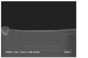
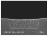
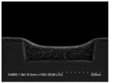
- the thickness of the polysiloxane coating film was 90 nm. Subsequently, about the obtained polysiloxane coating film, the cross-sectional shape was observed by cross-sectional SEM, and planarization property was evaluated. A groove pattern having a depth of 220 nm and a width of 800 nm is observed, and the film thickness (that is, the length from the interface on the side in contact with the silicon substrate film to the interface on the side in contact with the air of the polysiloxane coating film) is measured with respect to the groove bottom. The film thickness difference between the smallest part and the largest part was measured and the film thickness difference was calculated. The smaller the film thickness difference, the better the flatness.
- the SEM photographs used for the evaluation are shown in FIGS.
- each of the coating polysiloxane compositions of Examples A1 to A3 was applied onto the obtained first polysiloxane coating film, and then dried on a hot plate at 110 ° C. for 1 minute, whereby Comparative Example A1.
- a laminated film formed of two layers of the first polysiloxane coating film and the second polysiloxane coating film of any of Examples A1 to A3 was formed.
- the film thickness of the second polysiloxane coating film was 90 nm
- the film thickness of the laminated film was 180 nm in total with the film thickness of 90 nm of the first polysiloxane coating film of Comparative Example A1 previously applied.
- the cross-sectional shape was observed by cross-sectional SEM, and planarization property was evaluated.
- a groove pattern having a depth of 220 nm and a width of 800 nm was observed, and the film thickness (that is, the length from the interface on the side in contact with the silicon substrate film to the interface on the side in contact with the atmosphere of the second polysiloxane coating film)
- the film thickness difference between the smallest and largest parts was measured and the film thickness difference was calculated. The smaller the film thickness difference, the better the flatness.
- SEM photographs used for the evaluation are shown in FIGS.
- a general acrylic photo-nanoimprint resist was used as the nano-nanoimprint resist. It spin-coated on the quartz substrate, and baked for 1 minute with a 100 degreeC hotplate, and obtained the film for optical nanoimprint.
- NM-0801HB manufactured by Myeongchang Mechanism Co., Ltd.
- the mold used was made of silicon, and the pattern dimension was 500 nm.
- the mold is immersed in Optool (registered trademark) HD (manufactured by Daikin Industries, Ltd.) in advance, treated for 2 hours using a high-temperature and high-humidity device with a temperature of 90 ° C and a humidity of 90RH%, rinsed with pure water, and then air What was dried with was used.
- Optool registered trademark
- HD manufactured by Daikin Industries, Ltd.
- the optical nanoimprinting apparatus was installed in an optical nanoimprinting apparatus with a silicon mold adhered to the optical nanoimprinting coating film.
- Optical nanoimprint is always performed at 23 ° C. under conditions of a) pressurization up to 1,000 N over 10 seconds, b) exposure at 500 mJ / cm 2 using a high-pressure mercury lamp, c) pressure removal over 10 seconds, d) mold And the substrate were separated and released.
- the cross-sectional shape was observed by cross-sectional SEM, and planarization property was evaluated.
- Measure the film thickness that is, the film thickness of the shortest part and the largest part of the length of the polysiloxane coating film from the interface in contact with the quartz substrate film to the interface in contact with the atmosphere of the polysiloxane coating film. It was calculated and the flatness was evaluated as better as the film thickness difference was smaller.
- reaction solution is cooled to room temperature, 100 g of 4-methyl-2-pentanol is added to the reaction solution, and acetone, water, hydrochloric acid, and ethanol as a reaction byproduct are distilled off from the reaction solution under reduced pressure and concentrated.
- a 4-methyl-2-pentanol solution of a cohydrolyzed condensate (polysiloxane) was obtained. Solid content concentration was adjusted so that it might become 13 mass% in conversion of the solid residue in 140 degreeC. 20 mg of acetic acid was added to 15 g of the prepared polymer solution. The flask was transferred to an oil bath adjusted to 150 ° C., and reacted for 24 hours under heating and reflux.
- the weight average molecular weight Mw by GPC was 3,700 in terms of polystyrene.
- the obtained polysiloxane was a polysiloxane in which a part of silanol groups was capped with 4-methyl-2-pentanol.
- reaction solution is cooled to room temperature, 100 g of 4-methyl-2-pentanol is added to the reaction solution, and acetone, water, hydrochloric acid, and ethanol as a reaction byproduct are distilled off from the reaction solution under reduced pressure and concentrated.
- a methyl isobutyl carbinol solution of a cohydrolyzed condensate (polysiloxane) was obtained. Solid content concentration was adjusted so that it might become 13 mass% in conversion of the solid residue in 140 degreeC. 20 mg of acetic acid was added to 15 g of the prepared polymer solution. The flask was transferred to an oil bath adjusted to 150 ° C., and reacted for 48 hours under heating and reflux.
- the weight average molecular weight Mw by GPC was 5,300 in terms of polystyrene.
- the obtained polysiloxane was a polysiloxane in which a part of silanol groups was capped with 4-methyl-2-pentanol.
- reaction solution is cooled to room temperature, 100 g of 2-propanol is added to the reaction solution, acetone, water and hydrochloric acid, and ethanol as a reaction byproduct are distilled off from the reaction solution under reduced pressure and concentrated to perform cohydrolytic condensation.
- a 2-propanol solution of the product (polysiloxane) was obtained. Solid content concentration was adjusted so that it might become 13 mass% in conversion of the solid residue in 140 degreeC. 20 mg of acetic acid was added to 15 g of the prepared polymer solution. The flask was transferred to an oil bath adjusted to 150 ° C. and reacted for 12 hours under heating and reflux. The weight average molecular weight Mw by GPC was 6,000 in terms of polystyrene.
- the obtained polysiloxane was a polysiloxane in which a part of silanol groups was capped with 2-propanol.
- reaction solution is cooled to room temperature, 100 g of 1-methoxy-2-propanol is added to the reaction solution, acetone, water and hydrochloric acid, and ethanol as a reaction byproduct are distilled off from the reaction solution under reduced pressure and concentrated.
- a 1-methoxy-2-propanol solution of the cohydrolyzed condensate (polysiloxane) was obtained. Solid content concentration was adjusted so that it might become 13 mass% in conversion of the solid residue in 140 degreeC. 20 mg of acetic acid was added to 15 g of the prepared polymer solution. The flask was transferred to an oil bath adjusted to 150 ° C. and reacted for 12 hours under heating and reflux.
- the weight average molecular weight Mw by GPC was 4,000 in terms of polystyrene.
- the obtained polysiloxane was a polysiloxane in which a part of silanol groups was capped with 1-methoxy-2-propanol.
- reaction solution is cooled to room temperature, 100 g of 4-methyl-2-pentanol is added to the reaction solution, and acetone, water, hydrochloric acid, and ethanol as a reaction byproduct are distilled off from the reaction solution under reduced pressure and concentrated.
- a 4-methyl-2-pentanol solution of a cohydrolyzed condensate (polysiloxane) was obtained. Solid content concentration was adjusted so that it might become 13 mass% in conversion of the solid residue in 140 degreeC.
- the weight average molecular weight Mw by GPC was 1,400 in terms of polystyrene.
- the obtained polysiloxane was a polysiloxane in which a part of silanol groups was capped with 4-methyl-2-pentanol.
- the polymer solutions obtained in Synthesis Examples B1 to B4 and Comparative Synthesis Example B1 were diluted with 1-methoxy-2-propanol, 2-propanol or 1-methoxy-2-propanol to obtain a coating solution.
- the polymer content shown in Table 5 is not a polymer solution but a solid content obtained by removing the solvent from the polymer solution. The content ratio of each component is expressed in parts by mass.
- 4-methyl-2-pentanol, 2-propanol, and 1-methoxy-2-propanol are abbreviated as MIBC, IPA, and PGME, respectively.
- the evaluation results using the coating solution of the present invention are shown below. [Flatability of coating liquid (Evaluation of flatness on Si substrate)]
- the coating polysiloxane compositions in Examples B1 to B4 and Comparative Example B1 were evaluated for planarization as follows. The evaluation results are shown in Table 6.
- a groove pattern having a depth of 220 nm and a width of 800 nm is observed, and the film thickness, that is, the shortest part and the largest part of the length from the interface on the side in contact with the substrate film to the interface on the side in contact with the atmosphere of the polysiloxane coating film
- the film thickness at the location was measured, the film thickness difference was calculated, and the smaller the film thickness difference, the better the flatness.
- SEM photographs used for the evaluation are shown in FIGS.
- the mold is immersed in Optool (registered trademark) HD (manufactured by Daikin Industries, Ltd.) in advance, treated for 2 hours using a high-temperature and high-humidity device with a temperature of 90 ° C and a humidity of 90RH%, rinsed with pure water, and then air What was dried with was used.
- Optool registered trademark
- HD manufactured by Daikin Industries, Ltd.
- the silicon nanomold was adhered to the coating film for optical nanoimprinting, and the optical nanoimprinting apparatus was installed.
- Optical nanoimprint is always performed at 23 ° C. under conditions of a) pressurization up to 1,000 N over 10 seconds, b) exposure at 500 mJ / cm 2 using a high-pressure mercury lamp, c) pressure removal over 10 seconds, d)
- the mold and the substrate were separated and released in a sequence.
- the coating polysiloxane compositions in Examples B1 to B4 and Comparative Example B1 were evaluated for planarization as follows. The evaluation results are shown in Table 7.
- Each of the coating polysiloxane compositions of Examples B1 to B4 and Comparative Example B1 (coating composition) was applied onto the nanoimprint substrate using a spin coater under the conditions of a rotation speed of 1,500 rpm and 60 seconds. Then, it was dried on a hot plate at 110 ° C. for 1 minute to form a polysiloxane coating film with a coating polysiloxane composition (coating composition).
- the film thickness of the polysiloxane coating film by the coating polysiloxane composition was 120 nm.
- the cross-sectional shape was observed by cross-sectional SEM, and planarization property was evaluated.
- Measure the film thickness that is, the film thickness of the shortest part and the largest part of the length from the interface on the side in contact with the substrate film to the interface on the side in contact with the air of the polysiloxane coating film, and calculate the film thickness difference The smaller the film thickness difference, the better the flatness.
- Examples B1 to B4 a flat film having a film thickness difference of 30 nm or less, for example, about 5 to 30 nm can be formed.
Landscapes
- Chemical & Material Sciences (AREA)
- Engineering & Computer Science (AREA)
- Life Sciences & Earth Sciences (AREA)
- Wood Science & Technology (AREA)
- Chemical Kinetics & Catalysis (AREA)
- Materials Engineering (AREA)
- Organic Chemistry (AREA)
- General Physics & Mathematics (AREA)
- Physics & Mathematics (AREA)
- Architecture (AREA)
- Structural Engineering (AREA)
- Materials For Photolithography (AREA)
- Silicon Polymers (AREA)
- General Chemical & Material Sciences (AREA)
- Photosensitive Polymer And Photoresist Processing (AREA)
- Drying Of Semiconductors (AREA)
- Formation Of Insulating Films (AREA)
- Exposure Of Semiconductors, Excluding Electron Or Ion Beam Exposure (AREA)
Abstract
Priority Applications (4)
| Application Number | Priority Date | Filing Date | Title |
|---|---|---|---|
| JP2018501578A JP6835062B2 (ja) | 2016-02-24 | 2017-02-10 | シリコン含有組成物を用いた半導体基板の平坦化方法 |
| CN201780013335.9A CN108885997B (zh) | 2016-02-24 | 2017-02-10 | 使用了含硅组合物的半导体基板的平坦化方法 |
| US16/082,189 US10910220B2 (en) | 2016-02-24 | 2017-02-10 | Planarization method for a semiconductor substrate using a silicon-containing composition |
| KR1020187024381A KR102830156B1 (ko) | 2016-02-24 | 2017-02-10 | 실리콘 함유 조성물을 이용한 반도체 기판의 평탄화방법 |
Applications Claiming Priority (2)
| Application Number | Priority Date | Filing Date | Title |
|---|---|---|---|
| JP2016-033393 | 2016-02-24 | ||
| JP2016033393 | 2016-02-24 |
Publications (1)
| Publication Number | Publication Date |
|---|---|
| WO2017145808A1 true WO2017145808A1 (fr) | 2017-08-31 |
Family
ID=59686551
Family Applications (1)
| Application Number | Title | Priority Date | Filing Date |
|---|---|---|---|
| PCT/JP2017/004918 Ceased WO2017145808A1 (fr) | 2016-02-24 | 2017-02-10 | Procédé de planarisation pour substrats semi-conducteurs au moyen d'une composition contenant du silicium |
Country Status (6)
| Country | Link |
|---|---|
| US (1) | US10910220B2 (fr) |
| JP (1) | JP6835062B2 (fr) |
| KR (1) | KR102830156B1 (fr) |
| CN (1) | CN108885997B (fr) |
| TW (1) | TWI707400B (fr) |
| WO (1) | WO2017145808A1 (fr) |
Cited By (4)
| Publication number | Priority date | Publication date | Assignee | Title |
|---|---|---|---|---|
| JPWO2017043344A1 (ja) * | 2015-09-09 | 2018-07-19 | 日産化学工業株式会社 | シリコン含有平坦化性パターン反転用被覆剤 |
| WO2019126156A1 (fr) * | 2017-12-19 | 2019-06-27 | Honeywell International Inc. | Procédés, films et compositions de planarisation diélectrique à base de polysiloxane résistant à la fissuration |
| TWI690774B (zh) * | 2018-01-30 | 2020-04-11 | 日商旭化成股份有限公司 | 感光性樹脂積層體及抗蝕劑圖案之製造方法 |
| JP2020096168A (ja) * | 2018-09-21 | 2020-06-18 | 日産化学株式会社 | 固体撮像素子用平坦化膜形成樹脂組成物 |
Families Citing this family (5)
| Publication number | Priority date | Publication date | Assignee | Title |
|---|---|---|---|---|
| CN108699389B (zh) * | 2016-02-24 | 2020-10-27 | 日产化学株式会社 | 含有硅的图案反转用被覆剂 |
| CN113631281B (zh) * | 2019-02-14 | 2023-08-25 | 陶氏东丽株式会社 | 有机聚硅氧烷固化物膜、其用途、制备方法及制备装置 |
| US11656550B2 (en) | 2020-09-01 | 2023-05-23 | Tokyo Electron Limited | Controlling semiconductor film thickness |
| US12325046B2 (en) * | 2022-06-28 | 2025-06-10 | Canon Kabushiki Kaisha | Superstrate including a body and layers and methods of forming and using the same |
| FI131619B1 (en) * | 2022-10-12 | 2025-08-08 | Pibond Oy | Thin films with low dielectric constant, method for producing the same and use thereof |
Citations (6)
| Publication number | Priority date | Publication date | Assignee | Title |
|---|---|---|---|---|
| JPH01313942A (ja) * | 1988-06-14 | 1989-12-19 | Fujitsu Ltd | 半導体装置 |
| JPH10229079A (ja) * | 1996-12-20 | 1998-08-25 | Dow Corning Corp | 基材上にコーティングを形成する方法 |
| JPH10237307A (ja) * | 1997-02-24 | 1998-09-08 | Toray Dow Corning Silicone Co Ltd | シリカ薄膜形成用組成物およびシリカ薄膜の形成方法 |
| JPH113888A (ja) * | 1997-05-28 | 1999-01-06 | Texas Instr Inc <Ti> | 集積回路誘電体及び方法 |
| JPH11311865A (ja) * | 1998-03-23 | 1999-11-09 | Toshiba Corp | 段差をもった基板上の高精度レジストパターニング方法 |
| JP2001343757A (ja) * | 2000-03-28 | 2001-12-14 | Toshiba Corp | レジストパターンの形成方法 |
Family Cites Families (10)
| Publication number | Priority date | Publication date | Assignee | Title |
|---|---|---|---|---|
| EP0860462A3 (fr) | 1997-02-24 | 1999-04-21 | Dow Corning Toray Silicone Company Limited | Composition et procédé pour la formation d'un film mince de silice |
| US6008540A (en) | 1997-05-28 | 1999-12-28 | Texas Instruments Incorporated | Integrated circuit dielectric and method |
| US20100178620A1 (en) | 2007-05-21 | 2010-07-15 | Jsr Corporation | Inverted pattern forming method and resin composition |
| JP5365809B2 (ja) * | 2008-02-18 | 2013-12-11 | 日産化学工業株式会社 | 環状アミノ基を有するシリコン含有レジスト下層膜形成組成物 |
| JP5438958B2 (ja) | 2008-12-24 | 2014-03-12 | 東京応化工業株式会社 | パターン形成方法および反転パターン形成用材料 |
| JP5282920B2 (ja) * | 2009-04-24 | 2013-09-04 | 日産化学工業株式会社 | パターン反転膜形成用組成物及び反転パターン形成方法 |
| KR101674703B1 (ko) * | 2009-10-30 | 2016-11-09 | 제이에스알 가부시끼가이샤 | 반전 패턴 형성 방법 및 폴리실록산 수지 조성물 |
| JP5997041B2 (ja) * | 2012-12-26 | 2016-09-21 | 東京応化工業株式会社 | 感光性樹脂組成物 |
| JP5842841B2 (ja) * | 2013-02-18 | 2016-01-13 | 信越化学工業株式会社 | パターン形成方法 |
| JP6480691B2 (ja) * | 2013-10-21 | 2019-03-13 | アーゼッド・エレクトロニック・マテリアルズ(ルクセンブルグ)ソシエテ・ア・レスポンサビリテ・リミテ | ケイ素含有熱または光硬化性組成物 |
-
2017
- 2017-02-10 WO PCT/JP2017/004918 patent/WO2017145808A1/fr not_active Ceased
- 2017-02-10 TW TW106104491A patent/TWI707400B/zh active
- 2017-02-10 KR KR1020187024381A patent/KR102830156B1/ko active Active
- 2017-02-10 JP JP2018501578A patent/JP6835062B2/ja active Active
- 2017-02-10 US US16/082,189 patent/US10910220B2/en active Active
- 2017-02-10 CN CN201780013335.9A patent/CN108885997B/zh active Active
Patent Citations (6)
| Publication number | Priority date | Publication date | Assignee | Title |
|---|---|---|---|---|
| JPH01313942A (ja) * | 1988-06-14 | 1989-12-19 | Fujitsu Ltd | 半導体装置 |
| JPH10229079A (ja) * | 1996-12-20 | 1998-08-25 | Dow Corning Corp | 基材上にコーティングを形成する方法 |
| JPH10237307A (ja) * | 1997-02-24 | 1998-09-08 | Toray Dow Corning Silicone Co Ltd | シリカ薄膜形成用組成物およびシリカ薄膜の形成方法 |
| JPH113888A (ja) * | 1997-05-28 | 1999-01-06 | Texas Instr Inc <Ti> | 集積回路誘電体及び方法 |
| JPH11311865A (ja) * | 1998-03-23 | 1999-11-09 | Toshiba Corp | 段差をもった基板上の高精度レジストパターニング方法 |
| JP2001343757A (ja) * | 2000-03-28 | 2001-12-14 | Toshiba Corp | レジストパターンの形成方法 |
Cited By (6)
| Publication number | Priority date | Publication date | Assignee | Title |
|---|---|---|---|---|
| JPWO2017043344A1 (ja) * | 2015-09-09 | 2018-07-19 | 日産化学工業株式会社 | シリコン含有平坦化性パターン反転用被覆剤 |
| WO2019126156A1 (fr) * | 2017-12-19 | 2019-06-27 | Honeywell International Inc. | Procédés, films et compositions de planarisation diélectrique à base de polysiloxane résistant à la fissuration |
| US11015082B2 (en) | 2017-12-19 | 2021-05-25 | Honeywell International Inc. | Crack-resistant polysiloxane dielectric planarizing compositions, methods and films |
| TWI690774B (zh) * | 2018-01-30 | 2020-04-11 | 日商旭化成股份有限公司 | 感光性樹脂積層體及抗蝕劑圖案之製造方法 |
| JP2020096168A (ja) * | 2018-09-21 | 2020-06-18 | 日産化学株式会社 | 固体撮像素子用平坦化膜形成樹脂組成物 |
| JP7319588B2 (ja) | 2018-09-21 | 2023-08-02 | 日産化学株式会社 | 固体撮像素子用平坦化膜形成樹脂組成物 |
Also Published As
| Publication number | Publication date |
|---|---|
| CN108885997A (zh) | 2018-11-23 |
| US20190051518A1 (en) | 2019-02-14 |
| TWI707400B (zh) | 2020-10-11 |
| KR102830156B1 (ko) | 2025-07-07 |
| JP6835062B2 (ja) | 2021-02-24 |
| JPWO2017145808A1 (ja) | 2018-12-13 |
| TW201802944A (zh) | 2018-01-16 |
| KR20180118636A (ko) | 2018-10-31 |
| CN108885997B (zh) | 2023-06-02 |
| US10910220B2 (en) | 2021-02-02 |
Similar Documents
| Publication | Publication Date | Title |
|---|---|---|
| KR102426414B1 (ko) | Soc 패턴 상에서의 패턴반전을 위한 피복용 조성물 | |
| KR102830156B1 (ko) | 실리콘 함유 조성물을 이용한 반도체 기판의 평탄화방법 | |
| US12084592B2 (en) | Coating composition for pattern inversion | |
| JP7157392B2 (ja) | アルカリ性現像液可溶性シリコン含有レジスト下層膜形成組成物 | |
| WO2020138092A1 (fr) | Procédé d'amélioration de la résistance à la gravure d'un film de sous-couche de réserve par prétraitement à l'aide de gaz hydrogène | |
| JP6738049B2 (ja) | シリコン含有平坦化性パターン反転用被覆剤 | |
| JP7143763B2 (ja) | シリコン含有パターン反転用被覆剤 | |
| WO2017043635A1 (fr) | Composition de revêtement de motif de réserve comprenant du polysiloxane contenant un groupe vinyle ou un groupe (méth)acryloxy | |
| JP2020027841A (ja) | 光または電子線に応答するパターン反転組成物およびそれを用いたパターン形成方法 |
Legal Events
| Date | Code | Title | Description |
|---|---|---|---|
| ENP | Entry into the national phase |
Ref document number: 2018501578 Country of ref document: JP Kind code of ref document: A |
|
| ENP | Entry into the national phase |
Ref document number: 20187024381 Country of ref document: KR Kind code of ref document: A |
|
| NENP | Non-entry into the national phase |
Ref country code: DE |
|
| 121 | Ep: the epo has been informed by wipo that ep was designated in this application |
Ref document number: 17756249 Country of ref document: EP Kind code of ref document: A1 |
|
| 122 | Ep: pct application non-entry in european phase |
Ref document number: 17756249 Country of ref document: EP Kind code of ref document: A1 |