WO2017154171A1 - Dispositif d'acquisition d'image et procédé d'acquisition d'image - Google Patents
Dispositif d'acquisition d'image et procédé d'acquisition d'image Download PDFInfo
- Publication number
- WO2017154171A1 WO2017154171A1 PCT/JP2016/057578 JP2016057578W WO2017154171A1 WO 2017154171 A1 WO2017154171 A1 WO 2017154171A1 JP 2016057578 W JP2016057578 W JP 2016057578W WO 2017154171 A1 WO2017154171 A1 WO 2017154171A1
- Authority
- WO
- WIPO (PCT)
- Prior art keywords
- signal
- control unit
- light
- image acquisition
- periodic signal
- Prior art date
- Legal status (The legal status is an assumption and is not a legal conclusion. Google has not performed a legal analysis and makes no representation as to the accuracy of the status listed.)
- Ceased
Links
Images



Classifications
-
- G—PHYSICS
- G01—MEASURING; TESTING
- G01N—INVESTIGATING OR ANALYSING MATERIALS BY DETERMINING THEIR CHEMICAL OR PHYSICAL PROPERTIES
- G01N21/00—Investigating or analysing materials by the use of optical means, i.e. using sub-millimetre waves, infrared, visible or ultraviolet light
- G01N21/62—Systems in which the material investigated is excited whereby it emits light or causes a change in wavelength of the incident light
- G01N21/63—Systems in which the material investigated is excited whereby it emits light or causes a change in wavelength of the incident light optically excited
- G01N21/64—Fluorescence; Phosphorescence
-
- G—PHYSICS
- G01—MEASURING; TESTING
- G01N—INVESTIGATING OR ANALYSING MATERIALS BY DETERMINING THEIR CHEMICAL OR PHYSICAL PROPERTIES
- G01N21/00—Investigating or analysing materials by the use of optical means, i.e. using sub-millimetre waves, infrared, visible or ultraviolet light
- G01N21/62—Systems in which the material investigated is excited whereby it emits light or causes a change in wavelength of the incident light
- G01N21/63—Systems in which the material investigated is excited whereby it emits light or causes a change in wavelength of the incident light optically excited
- G01N21/64—Fluorescence; Phosphorescence
- G01N21/645—Specially adapted constructive features of fluorimeters
- G01N21/6456—Spatial resolved fluorescence measurements; Imaging
- G01N21/6458—Fluorescence microscopy
-
- G—PHYSICS
- G02—OPTICS
- G02B—OPTICAL ELEMENTS, SYSTEMS OR APPARATUS
- G02B21/00—Microscopes
-
- G—PHYSICS
- G02—OPTICS
- G02B—OPTICAL ELEMENTS, SYSTEMS OR APPARATUS
- G02B21/00—Microscopes
- G02B21/0004—Microscopes specially adapted for specific applications
- G02B21/002—Scanning microscopes
- G02B21/0024—Confocal scanning microscopes (CSOMs) or confocal "macroscopes"; Accessories which are not restricted to use with CSOMs, e.g. sample holders
- G02B21/0052—Optical details of the image generation
- G02B21/0076—Optical details of the image generation arrangements using fluorescence or luminescence
-
- G—PHYSICS
- G02—OPTICS
- G02B—OPTICAL ELEMENTS, SYSTEMS OR APPARATUS
- G02B21/00—Microscopes
- G02B21/0004—Microscopes specially adapted for specific applications
- G02B21/002—Scanning microscopes
- G02B21/0024—Confocal scanning microscopes (CSOMs) or confocal "macroscopes"; Accessories which are not restricted to use with CSOMs, e.g. sample holders
- G02B21/008—Details of detection or image processing, including general computer control
-
- G—PHYSICS
- G01—MEASURING; TESTING
- G01N—INVESTIGATING OR ANALYSING MATERIALS BY DETERMINING THEIR CHEMICAL OR PHYSICAL PROPERTIES
- G01N21/00—Investigating or analysing materials by the use of optical means, i.e. using sub-millimetre waves, infrared, visible or ultraviolet light
- G01N21/62—Systems in which the material investigated is excited whereby it emits light or causes a change in wavelength of the incident light
- G01N21/63—Systems in which the material investigated is excited whereby it emits light or causes a change in wavelength of the incident light optically excited
- G01N21/64—Fluorescence; Phosphorescence
- G01N21/645—Specially adapted constructive features of fluorimeters
- G01N2021/6463—Optics
Definitions
- the present invention relates to an image acquisition device and an image acquisition method.
- the present invention has been made in view of the above-described circumstances, and an image acquisition apparatus and an image acquisition method capable of obtaining necessary sensitivity in a shorter exposure time compared to the case of using a lock-in amplifier. The purpose is to provide.
- a scanning unit that scans illumination light emitted from a light source, and the illumination light that is scanned by the scanning unit is collected on a sample, while signal light generated at each scanning position of the sample
- An optical system that collects the light, a detector that detects the signal light collected by the optical system and generates a detection signal, a signal control unit that generates a periodic signal repeated at a predetermined period, and the signal
- a light control unit that temporally controls the position or intensity of the illumination light according to the periodic signal generated by the control unit, and the detection signal generated by the detector according to the periodic signal generated by the signal control unit
- a calculation unit that processes the frequency of the detection signal by the period of the periodic signal generated by the signal control unit, and before the shift by the frequency shift unit.
- a detection signal which is an image acquisition device comprising an integrator for integrating an integer multiple of the integration time period of the periodic signal.
- each scanning position of the sample is irradiated via the optical system, and the signal light generated at each scanning position is collected by the optical system. Lighted. The collected signal light is detected by a detector to generate a detection signal, and the generated detection signal is processed in the arithmetic unit.
- the light control unit controls the irradiation position and intensity of the illumination light on the sample in accordance with the periodic signal generated by the signal control unit.
- the signal control unit generates the frequency of the detection signal generated by the detector. After being shifted by the frequency shift means by the period of the periodic signal, the integrator is integrated with an integration time that is an integral multiple of the period of the periodic signal in the integrator. Thereby, arbitrary signals can be separated and extracted from the detection signals detected in the mixed state.
- a lock-in amplifier is not used for signal separation and extraction, and an integrator that operates according to a periodic signal generated by the signal control unit is used.
- the required refresh rate is no longer necessary, and a signal with the required sensitivity is extracted with a shorter exposure time, and the extracted signal is applied to each scanning position, whereby an image of the sample can be acquired.
- the light control unit may alternately switch the position or intensity of the illumination light between two states according to the periodic signal.
- the signal control unit is configured to link the other two with reference to the periodic signal input to any one of the light control unit, the frequency shift unit, and the integrator. The phase of the periodic signal input to the other two may be adjusted.
- the said signal control part may be provided in either the said light control part, the said frequency shift means, and the said integrator.
- an A / D converter for digitizing the detection signal is provided, the frequency shift means assigns a digital code to the detection signal according to the periodic signal, and the integrator performs digital integration. May be.
- the A / D converter may have an offset adjustment function.
- the resolution of the detection signal can be improved by the A / D converter having the offset function.
- the illumination light is irradiated to the sample via a plurality of paths, and at least one of the light control unit, the signal control unit, and the calculation unit is configured so that each of the route passing through the path A plurality may be provided corresponding to the illumination light.
- a modulation step for temporally controlling the position or intensity of illumination light emitted from a light source according to a periodic signal repeated at a predetermined cycle, and the illumination light controlled in the modulation step A scanning step for scanning the sample, a detection step for detecting a signal light generated at each scanning position of the illumination light scanned in the scanning step to generate a detection signal, and the detection signal generated in the detection step A frequency shift step that shifts the frequency of the periodic signal by the period of the periodic signal, and an integration step that integrates the detection signal shifted by the frequency shift step with an integral time that is an integral multiple of the period of the periodic signal. It is an acquisition method.
- FIG. 4 is a diagram illustrating detection signals after integration. It is a block diagram which shows the image acquisition method which concerns on one Embodiment of this invention. It is a block diagram which shows the 1st modification of the image acquisition apparatus of FIG. It is a block diagram which shows the 2nd modification of the image acquisition apparatus of FIG. It is a block diagram which shows the 3rd modification of the image acquisition apparatus of FIG. It is a block diagram which shows the 4th modification of the image acquisition apparatus of FIG. It is a block diagram which shows the 5th modification of the image acquisition apparatus of FIG.
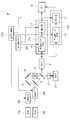
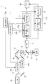
- the image acquisition apparatus 1 is a confocal microscope, and includes a light source 2 that emits laser light (illumination light), and a light control unit 3 that temporally modulates the position of the laser light from the light source 2. It has.
- the image acquisition apparatus 1 also collects a scanner (scanning unit) 4 that scans the laser beam temporally modulated by the light control unit 3 two-dimensionally and the laser beam scanned by the scanner 4 on the sample A.
- an objective lens (optical system) 5 that condenses the fluorescence generated at the irradiation position of the laser beam on the sample A is provided.
- the image acquisition device 1 also has a dichroic mirror 6 that separates the fluorescent light collected by the objective lens 5 and returned via the scanner 4 from the optical path of the laser light, and a position optically conjugate with the focal position of the objective lens 5.
- a pinhole 7 is provided, and a detector (PMT: photomultiplier tube) 8 that detects the fluorescence that has passed through the pinhole 7 and generates a detection signal.
- PMT photomultiplier tube
- the image acquisition apparatus 1 includes a calculation unit 9 that processes the detection signal generated by the detector 8 and an image processing unit (PC: personal computer) that generates an image based on the detection signal processed by the calculation unit 9. ) 10. Further, the light control unit 3 and the calculation unit 9 are connected to a signal control unit 11 that generates a predetermined periodic signal for synchronizing them.
- PC personal computer
- the light control unit 3 includes a first beam splitter 12 that branches the laser light from the light source 2 into two optical paths L1 and L2, and the optical paths L1 and L2 that are branched by the first beam splitter 12.
- a first beam splitter 12 that branches the laser light from the light source 2 into two optical paths L1 and L2, and the optical paths L1 and L2 that are branched by the first beam splitter 12.
- AOM acousto-optic modulators
- second beam splitter 14 for multiplexing the laser beams modulated by the acousto-optic modulators 13a and 13b.
- reference numeral 15 denotes a mirror for constituting an optical path.
- One optical path L1 is set so that the optical axis is shifted by the mirror 15 and the two laser beams combined by the second beam splitter 14 are incident on the scanner 4 at different angles.
- the laser beam that has passed through one optical path L1 is condensed at a position on the sample A that is optically non-conjugated with the pinhole 7.
- the laser beam that has passed through the other optical path L2 is condensed at a position on the sample A that is optically conjugate with the pinhole 7.
- the two acousto-optic modulators 13a and 13b operate exclusively according to the periodic signal output from the signal control unit 11.
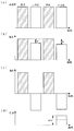
- the laser light emitted from the light source 2 is a timing at which the intensity of the laser light passing through the two optical paths L1 and L2 is inverted by operating the two acousto-optic modulators 13a and 13b in synchronization with the periodic signal.
- FIG. 2 (a) the laser beam focused on the conjugate position and the laser beam focused on the non-conjugated position are alternately generated as shown in FIG.
- the two states with different laser light positions can be switched alternately in time.
- the calculation unit 9 includes an A / D converter (not shown), a frequency shift unit 16, and an integrator 17.
- the detection signal detected by the detector 8 is converted into a digital signal by an A / D converter and then input to the frequency shift means 16.
- the frequency shift means 16 shifts the frequency of the detection signal generated by the detector 8 by the period of the periodic signal generated by the signal control unit 11.
- the frequency shift means 16 is a digital frequency shift means that assigns a sign at a timing synchronized with a periodic signal, but may be a method of assigning positive or negative by a switch in an electric circuit, but is not limited thereto. Is not to be done.
- the integrator 17 integrates the output from the frequency shift means 16 with an integration time that is an integral multiple of the period of the periodic signal generated by the signal control unit 11. In the example shown in FIG. 2, integration is performed with an integration time twice as long as the period of the periodic signal.
- the output from the integrator 17 is shown in FIG. Thereby, only the fluorescence generated by subtracting the out-of-focus fluorescence from the fluorescence obtained by mixing the fluorescence generated at the focal position of the objective lens 5 and the out-of-focus fluorescence generated outside the focus, that is, the fluorescence generated at the focal position of the objective lens 5 only. Can be calculated.
- the image processing unit 10 generates a fluorescence image of the sample A by associating the fluorescence intensity output from the calculation unit 9 with the scanning position information by the scanner 4 when the fluorescence is detected. Yes. Since the fluorescence intensity output from the calculation unit 9 does not include the intensity of the out-of-focus fluorescence, a clear fluorescence image with little noise can be acquired.
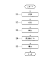
- the image acquisition method according to the present embodiment is modulated by a modulation step S1 that temporally modulates the position of the laser light emitted from the light source 2 in accordance with a periodic signal generated at a predetermined period generated by the signal control unit 11.
- a scanning step S2 for scanning the sample A with the laser beam by the scanner 4 a detection step S3 for generating a detection signal by detecting fluorescence generated at each scanning position of the scanned laser beam, and a detection signal
- the frequency shift step S4 for shifting the frequency by the period of the periodic signal generated by the signal control unit 11, and the shifted detection signal are integrated with an integral time that is an integral multiple of the period of the periodic signal generated by the signal control unit 11. Integration step S5.
- the arithmetic unit 9 demodulates the fluorescence generated from the focal position of the objective lens 5 by the frequency shift means 16 and the integrator 17. Therefore, the refresh rate required when using the lock-in amplifier is unnecessary, and there is an advantage that a fluorescent image having a necessary sensitivity can be acquired with a short exposure time. On the contrary, there is an advantage that a sufficiently bright fluorescent image can be acquired by performing exposure with an exposure time for obtaining a fluorescent image having a necessary sensitivity by a lock-in amplifier.
- the present invention is not limited to this.
- the signal control unit 11 uses a periodic signal input to any one of the light control unit 3, the frequency shift unit 16, and the integrator 17 as a reference, and inputs the other two to interlock with the other two. You may have the phase adjustment function which adjusts the phase of a signal.
- the signal control unit 11 is described as a separate device from the light control unit 3, the frequency shift unit 16, and the integrator 17, but instead, the signal control unit 11 includes the light control unit 3, the frequency shift unit, and the frequency shift unit 16. Any one of the means 16 and the integrator 17 may be provided.
- the signal control unit 11 is provided in the light control unit 3, and the light control unit 3 is controlled by a periodic signal generated by itself, and the frequency shift means 16 and the integrator are controlled by the periodic signal generated by the light control unit 3. 17 may be controlled.
- a digital frequency shifter is adopted as the frequency shift means 16 of the arithmetic unit 9 and a digital integrator is adopted as the integrator 17. Since code assignment is performed by software after A / D conversion, there is an advantage that frequency shift can be performed without changing hardware even if the waveform of the signal changes.
- a multiplier made of an analog circuit may be adopted as the frequency shift means 16 and an integrator made of an analog circuit may be adopted as the integrator 17.
- an integrator made of an analog circuit may be adopted as the integrator 17.
- the frequency shift means 16 a multiplier made of an analog circuit may be adopted, an A / D converter for converting the output of the multiplier into a digital signal may be provided, and a digital integrator may be adopted.
- the A / D converter that converts the detection signal detected by the detector 8 into a digital signal is preferably provided with an offset adjustment function.
- the acoustooptic modulators 13a and 13b are used as the light control unit 3 has been exemplified.
- a combination with a plate or the like may be used.
- the laser light source itself may be directly controlled.
- a device that changes the direction of laser light such as an acousto-optic polarizer or an electro-optic polarizer, may be employed.
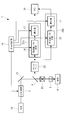
- the light source 18 is a laser light source that emits an ultrashort pulse laser beam
- the dichroic mirror 6 that branches fluorescence from the optical path of the ultrashort pulse laser beam is disposed between the objective lens 5 and the scanner 4.
- the pinhole 7 provided in FIG. 1 is excluded.
- two laser light sources (light sources) 19a and 19b that emit ultra-short pulse laser beams having different wavelengths, and ultra-short pulse laser beams from the laser light sources 19a and 19b, respectively, have different patterns.
- Two light control units 20a and 20b to modulate, two calculation units 21a and 21b that demodulate desired fluorescence from detected fluorescence, and two pairs of light control units 20a and 20b and calculation units 21a and 21b are different.
- Two signal controllers 22a and 22b for supplying periodic signals are provided. Thereby, two fluorescence signals can be acquired simultaneously.
- two pairs of signal control units 22a and 22b, light control units 20a and 20b, and arithmetic units 21a and 21b are provided, three or more pairs may be provided instead.
- only two calculation units 21 a and 21 b are provided, and the single light control unit 3 and the two pairs of calculation units 21 a and 21 b are synchronized by a periodic signal from the single signal control unit 11. May be activated.
- a multi-point scanner such as a Nipou disk is employed as the scanner 22, and a sensor array is employed as the detector 23.
- Two arithmetic units 21a and 21b are provided corresponding to the laser light passing through a plurality of optical paths branched by the Nipkow disk.
- the light modulation controls the light source intensity, switches the saturation / non-saturation of the focused fluorescence, and images the difference between the saturation / non-saturation, thereby improving resolution.
- two pairs of light sources 19a and 19b and light control units 20a and 20b are provided, and two light control units 20a and 20b and a single calculation unit 9 are connected to a single signal control unit 11.
- an SRS (Stimulated Raman Scattering) microscope that uses the vibration of the molecules of the sample A generated by the frequency difference when two types of laser beams having different frequencies are superimposed and irradiated onto the sample A is used. It can be applied to a nonlinear microscope.
- the two light sources 19a and 19b are laser light sources that emit ultrashort pulse laser beams having different wavelengths, respectively, and the periodic signal to the arithmetic unit 9 modulates one of the ultrashort pulse laser beams.
- the light control unit 20a Synchronized with the periodic signal to.
- a single laser light source 24 that emits an ultrashort pulse laser beam is adopted, and the two beams branched by the beam splitter 12 are used.
- the light control units 20a and 20b may be arranged on the two optical paths L1 and L2, respectively.
- two laser light sources 19a and 19b that emit an ultrashort pulse laser beam having the same wavelength may be employed.
Landscapes
- Physics & Mathematics (AREA)
- Chemical & Material Sciences (AREA)
- Analytical Chemistry (AREA)
- General Physics & Mathematics (AREA)
- Health & Medical Sciences (AREA)
- Optics & Photonics (AREA)
- Biochemistry (AREA)
- Life Sciences & Earth Sciences (AREA)
- Nuclear Medicine, Radiotherapy & Molecular Imaging (AREA)
- General Health & Medical Sciences (AREA)
- Immunology (AREA)
- Pathology (AREA)
- Engineering & Computer Science (AREA)
- Computer Vision & Pattern Recognition (AREA)
- General Engineering & Computer Science (AREA)
- Microscoopes, Condenser (AREA)
- Investigating, Analyzing Materials By Fluorescence Or Luminescence (AREA)
Abstract
Dans le but d'obtenir la sensibilité nécessaire dans un temps d'exposition plus court que lorsqu'un amplificateur de verrouillage est utilisé, le dispositif d'acquisition d'image (1) selon la présente invention comprend une unité de balayage (4) pour balayer avec une lumière d'éclairage émise par une source de lumière (2), un système optique (5) pour condenser la lumière d'éclairage balayée sur un échantillon (A) tout en condensant également une lumière de signal générée dans chaque position de balayage de l'échantillon (A), un détecteur (8) pour détecter la lumière de signal condensée et générer un signal de détection, une unité de commande de signal (11) pour générer un signal périodique répété à une période prédéterminée, une unité de commande de lumière (3) pour commander temporellement la position ou l'intensité de la lumière d'éclairage conformément au signal périodique généré, et une unité de calcul (9) pour traiter le signal de détection généré par le détecteur (8) conformément au signal périodique généré, l'unité de calcul (9) comprenant un moyen de décalage de fréquence (16) pour décaler la fréquence du signal de détection d'une période du signal périodique, et un intégrateur (17) pour intégrer le signal de détection décalé pendant un temps d'intégrale qui est un multiple entier de la période du signal périodique.
Priority Applications (3)
| Application Number | Priority Date | Filing Date | Title |
|---|---|---|---|
| JP2018503945A JP6599539B2 (ja) | 2016-03-10 | 2016-03-10 | 画像取得装置および画像取得方法 |
| PCT/JP2016/057578 WO2017154171A1 (fr) | 2016-03-10 | 2016-03-10 | Dispositif d'acquisition d'image et procédé d'acquisition d'image |
| US16/102,840 US10261299B2 (en) | 2016-03-10 | 2018-08-14 | Image-acquisition apparatus and image-acquisition method |
Applications Claiming Priority (1)
| Application Number | Priority Date | Filing Date | Title |
|---|---|---|---|
| PCT/JP2016/057578 WO2017154171A1 (fr) | 2016-03-10 | 2016-03-10 | Dispositif d'acquisition d'image et procédé d'acquisition d'image |
Related Child Applications (1)
| Application Number | Title | Priority Date | Filing Date |
|---|---|---|---|
| US16/102,840 Continuation US10261299B2 (en) | 2016-03-10 | 2018-08-14 | Image-acquisition apparatus and image-acquisition method |
Publications (1)
| Publication Number | Publication Date |
|---|---|
| WO2017154171A1 true WO2017154171A1 (fr) | 2017-09-14 |
Family
ID=59789280
Family Applications (1)
| Application Number | Title | Priority Date | Filing Date |
|---|---|---|---|
| PCT/JP2016/057578 Ceased WO2017154171A1 (fr) | 2016-03-10 | 2016-03-10 | Dispositif d'acquisition d'image et procédé d'acquisition d'image |
Country Status (3)
| Country | Link |
|---|---|
| US (1) | US10261299B2 (fr) |
| JP (1) | JP6599539B2 (fr) |
| WO (1) | WO2017154171A1 (fr) |
Cited By (1)
| Publication number | Priority date | Publication date | Assignee | Title |
|---|---|---|---|---|
| JP2024510596A (ja) * | 2021-03-11 | 2024-03-08 | ザ・トラスティーズ・オブ・コロンビア・ユニバーシティ・イン・ザ・シティ・オブ・ニューヨーク | 掃引共焦点配置平面励起(scape)顕微鏡法 |
Families Citing this family (1)
| Publication number | Priority date | Publication date | Assignee | Title |
|---|---|---|---|---|
| US12248133B2 (en) * | 2021-01-22 | 2025-03-11 | The Hong Kong University Of Science And Technology | Methods and apparatus for in vivo high resolution multiphoton microscopy |
Citations (3)
| Publication number | Priority date | Publication date | Assignee | Title |
|---|---|---|---|---|
| JP2011199939A (ja) * | 2010-03-17 | 2011-10-06 | Hitachi Ltd | 電力変換装置および電力変換装置の制御方法 |
| JP2014120862A (ja) * | 2012-12-14 | 2014-06-30 | Sony Corp | 通信装置 |
| WO2015163261A1 (fr) * | 2014-04-24 | 2015-10-29 | オリンパス株式会社 | Microscope et procédé d'observation microscopique |
Family Cites Families (17)
| Publication number | Priority date | Publication date | Assignee | Title |
|---|---|---|---|---|
| GB0200819D0 (en) * | 2002-01-15 | 2002-03-06 | Cole Polytechnique Federale De | Microscopy imaging apparatus and method for generating an image |
| WO2006061947A1 (fr) | 2004-12-08 | 2006-06-15 | Osaka University | Microscope a fluorescence et procede d’observation |
| JP5448353B2 (ja) * | 2007-05-02 | 2014-03-19 | キヤノン株式会社 | 光干渉断層計を用いた画像形成方法、及び光干渉断層装置 |
| US8111455B2 (en) | 2007-11-26 | 2012-02-07 | Olympus Corporation | Light source apparatus and laser scanning microscope |
| JP5231154B2 (ja) | 2007-11-26 | 2013-07-10 | オリンパス株式会社 | レーザ走査型顕微鏡 |
| DE102008059328A1 (de) * | 2008-11-27 | 2010-06-02 | Carl Zeiss Microimaging Gmbh | Auflösungsgesteigerte Mikroskopie |
| US8531677B2 (en) * | 2010-05-27 | 2013-09-10 | Corning Incorporated | Frequency-shifting interferometer with selective data processing |
| DE102010047237B4 (de) | 2010-08-13 | 2021-07-01 | Leica Microsystems Cms Gmbh | Verfahren zum Trennen von Detektionssignalen im Strahlengang einer optischen Einrichtung |
| JP5412394B2 (ja) * | 2010-09-30 | 2014-02-12 | オリンパス株式会社 | 標本観察装置 |
| US9506749B2 (en) * | 2010-11-15 | 2016-11-29 | Seikowave, Inc. | Structured light 3-D measurement module and system for illuminating an area-under-test using a fixed-pattern optic |
| WO2012121357A1 (fr) | 2011-03-04 | 2012-09-13 | Canon Kabushiki Kaisha | Appareil de détection de diffusion raman stimulée |
| WO2012153495A1 (fr) * | 2011-05-06 | 2012-11-15 | 株式会社ニコン | Microscope à éclairage structuré et procédé de visualisation à éclairage structuré |
| JP2014038031A (ja) | 2012-08-16 | 2014-02-27 | Fujifilm Corp | ラマン散乱光測定装置および方法 |
| ES2581554T3 (es) * | 2012-09-10 | 2016-09-06 | Philips Lighting Holding B.V. | Sistema y método de detección de luz |
| JP6058477B2 (ja) * | 2013-06-14 | 2017-01-11 | 東芝メディカルシステムズ株式会社 | 磁気共鳴イメージング装置 |
| WO2015030202A1 (fr) | 2013-08-30 | 2015-03-05 | 国立大学法人電気通信大学 | Dispositif de mesure optique, procédé de mesure optique, et système d'imagerie microscopique |
| WO2017022096A1 (fr) | 2015-08-05 | 2017-02-09 | オリンパス株式会社 | Microscope et procédé d'acquisition d'image |
-
2016
- 2016-03-10 WO PCT/JP2016/057578 patent/WO2017154171A1/fr not_active Ceased
- 2016-03-10 JP JP2018503945A patent/JP6599539B2/ja not_active Expired - Fee Related
-
2018
- 2018-08-14 US US16/102,840 patent/US10261299B2/en not_active Expired - Fee Related
Patent Citations (3)
| Publication number | Priority date | Publication date | Assignee | Title |
|---|---|---|---|---|
| JP2011199939A (ja) * | 2010-03-17 | 2011-10-06 | Hitachi Ltd | 電力変換装置および電力変換装置の制御方法 |
| JP2014120862A (ja) * | 2012-12-14 | 2014-06-30 | Sony Corp | 通信装置 |
| WO2015163261A1 (fr) * | 2014-04-24 | 2015-10-29 | オリンパス株式会社 | Microscope et procédé d'observation microscopique |
Cited By (2)
| Publication number | Priority date | Publication date | Assignee | Title |
|---|---|---|---|---|
| JP2024510596A (ja) * | 2021-03-11 | 2024-03-08 | ザ・トラスティーズ・オブ・コロンビア・ユニバーシティ・イン・ザ・シティ・オブ・ニューヨーク | 掃引共焦点配置平面励起(scape)顕微鏡法 |
| JP7849055B2 (ja) | 2021-03-11 | 2026-04-21 | ザ・トラスティーズ・オブ・コロンビア・ユニバーシティ・イン・ザ・シティ・オブ・ニューヨーク | 掃引共焦点配置平面励起(scape)顕微鏡法 |
Also Published As
| Publication number | Publication date |
|---|---|
| US20190004302A1 (en) | 2019-01-03 |
| US10261299B2 (en) | 2019-04-16 |
| JPWO2017154171A1 (ja) | 2018-12-27 |
| JP6599539B2 (ja) | 2019-10-30 |
Similar Documents
| Publication | Publication Date | Title |
|---|---|---|
| US9356413B2 (en) | Laser source apparatus and laser microscope | |
| JP2015522850A (ja) | 光学顕微鏡およびその制御方法 | |
| JP6720165B2 (ja) | 画像取得装置および画像取得方法 | |
| US20080192128A1 (en) | Device and Method for Generating an Image of an Object | |
| JP6599539B2 (ja) | 画像取得装置および画像取得方法 | |
| EP3141942B1 (fr) | Microscope à laser et procédé de microscopie | |
| JP5179099B2 (ja) | 光刺激用照明装置および顕微鏡装置 | |
| JP2016038218A (ja) | 光学測定装置及び光学測定方法 | |
| US10942345B2 (en) | Image acquisition method and image acquisition device | |
| JP2005091895A (ja) | 走査型共焦点顕微鏡装置 | |
| JP6257156B2 (ja) | 顕微鏡装置 | |
| WO2017175374A1 (fr) | Dispositif d'acquisition d'image | |
| JP6777160B2 (ja) | 蛍光観察装置 | |
| JP5191352B2 (ja) | レーザ走査型顕微鏡 | |
| JP6065517B2 (ja) | 蛍光顕微鏡、蛍光検出方法、及び蛍光検出ユニット | |
| JP6673497B2 (ja) | 蛍光観察装置 | |
| JP2007232713A (ja) | 試料を高い空間分解能で検査するための方法 | |
| JP7268144B2 (ja) | 試料を走査する方法および装置 | |
| JP5831782B2 (ja) | 顕微鏡装置 | |
| JP2016033676A (ja) | 顕微鏡装置 | |
| JP2004219513A (ja) | レーザ顕微鏡 | |
| JPWO2018083772A1 (ja) | 顕微鏡システム | |
| JP5655434B2 (ja) | 観察装置及び観察方法 | |
| JP6643896B2 (ja) | 光パルス列同期装置、光学顕微鏡及び光パルス列同期方法 | |
| JP4468642B2 (ja) | 共焦点レーザ走査型顕微鏡装置及び試料情報記録方法 |
Legal Events
| Date | Code | Title | Description |
|---|---|---|---|
| WWE | Wipo information: entry into national phase |
Ref document number: 2018503945 Country of ref document: JP |
|
| NENP | Non-entry into the national phase |
Ref country code: DE |
|
| 121 | Ep: the epo has been informed by wipo that ep was designated in this application |
Ref document number: 16893500 Country of ref document: EP Kind code of ref document: A1 |
|
| 122 | Ep: pct application non-entry in european phase |
Ref document number: 16893500 Country of ref document: EP Kind code of ref document: A1 |