WO2017154404A1 - Dispositif optique à semi-conducteurs et procédé pour sa fabrication - Google Patents
Dispositif optique à semi-conducteurs et procédé pour sa fabrication Download PDFInfo
- Publication number
- WO2017154404A1 WO2017154404A1 PCT/JP2017/003190 JP2017003190W WO2017154404A1 WO 2017154404 A1 WO2017154404 A1 WO 2017154404A1 JP 2017003190 W JP2017003190 W JP 2017003190W WO 2017154404 A1 WO2017154404 A1 WO 2017154404A1
- Authority
- WO
- WIPO (PCT)
- Prior art keywords
- layer
- semiconductor
- wiring electrode
- semiconductor layer
- optical device
- Prior art date
- Legal status (The legal status is an assumption and is not a legal conclusion. Google has not performed a legal analysis and makes no representation as to the accuracy of the status listed.)
- Ceased
Links
Images

Classifications
-
- H—ELECTRICITY
- H10—SEMICONDUCTOR DEVICES; ELECTRIC SOLID-STATE DEVICES NOT OTHERWISE PROVIDED FOR
- H10H—INORGANIC LIGHT-EMITTING SEMICONDUCTOR DEVICES HAVING POTENTIAL BARRIERS
- H10H20/00—Individual inorganic light-emitting semiconductor devices having potential barriers, e.g. light-emitting diodes [LED]
- H10H20/80—Constructional details
- H10H20/83—Electrodes
- H10H20/831—Electrodes characterised by their shape
-
- H—ELECTRICITY
- H10—SEMICONDUCTOR DEVICES; ELECTRIC SOLID-STATE DEVICES NOT OTHERWISE PROVIDED FOR
- H10F—INORGANIC SEMICONDUCTOR DEVICES SENSITIVE TO INFRARED RADIATION, LIGHT, ELECTROMAGNETIC RADIATION OF SHORTER WAVELENGTH OR CORPUSCULAR RADIATION
- H10F30/00—Individual radiation-sensitive semiconductor devices in which radiation controls the flow of current through the devices, e.g. photodetectors
- H10F30/20—Individual radiation-sensitive semiconductor devices in which radiation controls the flow of current through the devices, e.g. photodetectors the devices having potential barriers, e.g. phototransistors
-
- H—ELECTRICITY
- H10—SEMICONDUCTOR DEVICES; ELECTRIC SOLID-STATE DEVICES NOT OTHERWISE PROVIDED FOR
- H10H—INORGANIC LIGHT-EMITTING SEMICONDUCTOR DEVICES HAVING POTENTIAL BARRIERS
- H10H20/00—Individual inorganic light-emitting semiconductor devices having potential barriers, e.g. light-emitting diodes [LED]
- H10H20/80—Constructional details
- H10H20/81—Bodies
- H10H20/819—Bodies characterised by their shape, e.g. curved or truncated substrates
-
- H—ELECTRICITY
- H10—SEMICONDUCTOR DEVICES; ELECTRIC SOLID-STATE DEVICES NOT OTHERWISE PROVIDED FOR
- H10H—INORGANIC LIGHT-EMITTING SEMICONDUCTOR DEVICES HAVING POTENTIAL BARRIERS
- H10H20/00—Individual inorganic light-emitting semiconductor devices having potential barriers, e.g. light-emitting diodes [LED]
- H10H20/80—Constructional details
- H10H20/81—Bodies
- H10H20/819—Bodies characterised by their shape, e.g. curved or truncated substrates
- H10H20/82—Roughened surfaces, e.g. at the interface between epitaxial layers
-
- H—ELECTRICITY
- H10—SEMICONDUCTOR DEVICES; ELECTRIC SOLID-STATE DEVICES NOT OTHERWISE PROVIDED FOR
- H10H—INORGANIC LIGHT-EMITTING SEMICONDUCTOR DEVICES HAVING POTENTIAL BARRIERS
- H10H20/00—Individual inorganic light-emitting semiconductor devices having potential barriers, e.g. light-emitting diodes [LED]
- H10H20/80—Constructional details
- H10H20/83—Electrodes
- H10H20/832—Electrodes characterised by their material
-
- H—ELECTRICITY
- H10—SEMICONDUCTOR DEVICES; ELECTRIC SOLID-STATE DEVICES NOT OTHERWISE PROVIDED FOR
- H10H—INORGANIC LIGHT-EMITTING SEMICONDUCTOR DEVICES HAVING POTENTIAL BARRIERS
- H10H20/00—Individual inorganic light-emitting semiconductor devices having potential barriers, e.g. light-emitting diodes [LED]
- H10H20/80—Constructional details
- H10H20/85—Packages
- H10H20/855—Optical field-shaping means, e.g. lenses
-
- H—ELECTRICITY
- H10—SEMICONDUCTOR DEVICES; ELECTRIC SOLID-STATE DEVICES NOT OTHERWISE PROVIDED FOR
- H10H—INORGANIC LIGHT-EMITTING SEMICONDUCTOR DEVICES HAVING POTENTIAL BARRIERS
- H10H20/00—Individual inorganic light-emitting semiconductor devices having potential barriers, e.g. light-emitting diodes [LED]
- H10H20/80—Constructional details
- H10H20/85—Packages
- H10H20/857—Interconnections, e.g. lead-frames, bond wires or solder balls
-
- H—ELECTRICITY
- H10—SEMICONDUCTOR DEVICES; ELECTRIC SOLID-STATE DEVICES NOT OTHERWISE PROVIDED FOR
- H10H—INORGANIC LIGHT-EMITTING SEMICONDUCTOR DEVICES HAVING POTENTIAL BARRIERS
- H10H20/00—Individual inorganic light-emitting semiconductor devices having potential barriers, e.g. light-emitting diodes [LED]
- H10H20/01—Manufacture or treatment
- H10H20/032—Manufacture or treatment of electrodes
-
- H—ELECTRICITY
- H10—SEMICONDUCTOR DEVICES; ELECTRIC SOLID-STATE DEVICES NOT OTHERWISE PROVIDED FOR
- H10H—INORGANIC LIGHT-EMITTING SEMICONDUCTOR DEVICES HAVING POTENTIAL BARRIERS
- H10H20/00—Individual inorganic light-emitting semiconductor devices having potential barriers, e.g. light-emitting diodes [LED]
- H10H20/01—Manufacture or treatment
- H10H20/036—Manufacture or treatment of packages
Definitions
- the present invention relates to a semiconductor optical device and a manufacturing method thereof.
- LED semiconductor light emitting element
- a light emitting semiconductor optical device As light-receiving semiconductor optical devices, semiconductor light-receiving elements that convert optical signals and optical energy into electrical signals, solar cells that convert optical energy such as sunlight into electrical energy, and the like are known.
- a current is passed through a pn junction to convert light into light energy to emit light.
- a technique for improving the light extraction efficiency of light emitted from the light emitting layer in the semiconductor layer is required.
- the light receiving type semiconductor light receiving element and the solar cell In order to improve the light collection efficiency or increase the sensitivity of the semiconductor light receiving element, and to improve the light conversion efficiency of the solar cell, a technology for improving the light capturing efficiency is required. As a technique for improving such light extraction efficiency or light capture efficiency, roughening of the light emitting surface and the light receiving surface is known.
- Patent Document 1 includes a light emitting layer and a surface layer that includes a Ga (1-x) Al x As layer (0 ⁇ x ⁇ 0.8) and extracts light emitted from the light emitting layer to the outside.
- a method for manufacturing a semiconductor light emitting device is disclosed in which a semiconductor laminate is immersed in an aqueous nitric acid solution to roughen the surface of the surface layer. According to the technique of Patent Document 1, it is possible to manufacture a semiconductor light emitting device with an increased light output by improving the light extraction efficiency from the inside of the semiconductor crystal.
- Patent Document 2 discloses an infrared sensor having an infrared transmission part and an infrared detection part in which the outer surface of the infrared transmission part is an uneven surface.
- a semiconductor light-emitting element is generally configured by electrically sandwiching a semiconductor laminate including an n-type semiconductor layer, a light-emitting layer (also referred to as an active layer) and a p-type semiconductor layer between a pair of electrode portions.
- a semiconductor light emitting element is disclosed in Patent Document 3. That is, a conductive support substrate, and a light emitting portion made of an InGaAlP-based semiconductor including a metal layer, an n-type cladding layer, an active layer, and a p-type cladding layer on the conductive support substrate, and a current on the light emitting portion.
- a first ohmic wiring electrode portion is formed between the metal layer and the light emitting portion.
- a pedestal electrode and a second ohmic wiring electrode part are provided on the light extraction surface, and a connection thin line pattern for electrically connecting the pedestal electrode and the second ohmic wiring electrode part is formed.
- the present inventor paid attention to the line width of the wiring electrode portion among the electrodes provided on the surface of the semiconductor layer in order to improve the light extraction efficiency and the light capture efficiency of the semiconductor optical device. This is because if the line width of the wiring electrode portion is made smaller than the conventionally used line width, the area shielded by the electrode portion is reduced, that is, if the semiconductor light emitting element is a light emitting semiconductor optical device, light emission is achieved. This is because it is thought that the light extraction efficiency can be improved because the light emission area on the surface increases.
- Patent Document 3 in a semiconductor light emitting device in which an intermediate electrode is formed between a metal layer and a light emitting portion, and a pad electrode and a wiring electrode portion are provided on the light emitting surface, a current is applied to the electrode peripheral portion of the light emitting surface.
- the present inventors thought that the light emission output at the electrode peripheral portion is large due to the concentration of light, and that the improvement effect of the light extraction efficiency by reducing the line width is remarkably large. Further, the present inventor has also considered that in a semiconductor light receiving element and a solar cell, which are light receiving type semiconductor optical devices, the light capturing efficiency can be improved by reducing the line width of the wiring electrode portion.
- an object of the present invention is to provide a semiconductor optical device having a light extraction efficiency or a light capturing efficiency superior to those of the prior art and having a reduced peeling rate of a wiring electrode portion, and a manufacturing method thereof.
- the present inventor diligently studied on how to solve the above problems, and in order to reduce the peeling rate of the wiring electrode part, pay attention to the structure of the wiring electrode part including the metal layer and provide a protective layer having an anti-peeling effect. I recalled that. And when this inventor earnestly examined, it discovered that the peeling rate of a wiring electrode part can be reduced significantly by providing a conductive hard film as a protective layer on a metal layer, and came to complete this invention. .
- the gist of the present invention is as follows.
- a semiconductor optical device in which a wiring electrode portion is provided on the surface of a semiconductor layer to be a light emitting surface or a light receiving surface, The line width of the wiring electrode portion is 2 ⁇ m or more and 5 ⁇ m or less, The wiring electrode portion has a metal layer on the semiconductor layer, and a conductive hard film on the metal layer, The semiconductor optical device characterized in that the conductive hard film has a hardness higher than that of the metal layer.
- the surface of the semiconductor layer includes a flat surface region and a rough surface region,
- the surface of the semiconductor layer at the junction center between the surface of the semiconductor layer and the wiring electrode portion is the flat surface region, and the gap is configured by the rough surface region.
- the conductive hard film is a nitride of one or more metal elements selected from the group consisting of Ti, Ta, Cr, W, Mo, and V. (1) to (6 The semiconductor optical device according to any one of the above.
- the semiconductor layer includes an n-type semiconductor layer, a light emitting layer, and a p-type semiconductor layer, and the surface is the surface of either the n-type semiconductor layer or the p-type semiconductor layer.
- a method of manufacturing a semiconductor optical device including a wiring electrode part forming step of forming a wiring electrode part on a surface of a semiconductor layer to be a light emitting surface or a light receiving surface,
- the line width of the wiring electrode portion is 2 ⁇ m or more and 5 ⁇ m or less
- the wiring electrode portion forming step includes a first step of forming a metal layer on the surface of the semiconductor layer and a second step of forming a conductive hard film on the metal layer.
- the surface of the semiconductor layer is wet-etched to roughen the surface of the semiconductor layer located below the peripheral edge of the wiring electrode portion and form the gap.
- the semiconductor having the light extraction efficiency or the light capturing efficiency superior to the conventional one and the wiring electrode portion peeling rate is reduced.
- An optical device and a manufacturing method thereof can be provided.
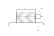
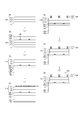
- FIG. 1 It is a schematic cross section which expands and shows the wiring electrode part of the semiconductor optical device 100 according to 1st Embodiment of this invention. It is a schematic diagram for explaining the line width W 1 herein.
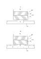
- (A), (B) is a schematic cross section which expands and shows the wiring electrode part of the semiconductor optical devices 200 and 200 'according to the one aspect
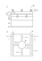
- (A) is a schematic cross-sectional view showing a semiconductor light emitting device 300 according to the second embodiment of the present invention, and (B) is a top view of the semiconductor light emitting device 300 shown in (A).
- (A) to (G) are schematic cross-sectional views showing an example of the manufacturing process of the semiconductor light emitting device 400 according to the third embodiment of the present invention. It is a microscope picture of an example of the semiconductor light-emitting device in an Example.
- the semiconductor optical device 100 As shown in FIG. 1, the semiconductor optical device 100 according to the first embodiment of the present invention is provided with a wiring electrode portion 120 on the surface of a semiconductor layer 110 serving as a light emitting surface or a light receiving surface.
- the line width W 1 of the wiring electrode part 120 is 2 ⁇ m or more and 5 ⁇ m or less, and this wiring electrode part 120 has a metal layer 121 on the semiconductor layer 110 and a conductive hard film 122 on the metal layer 121.
- the conductive hard film 122 is harder than the metal layer 121.
- the wiring pattern of the wiring electrode unit 120 is not limited at all. Like the wiring pattern of the wiring electrode portion 120 in the semiconductor light emitting element 300 described later with reference to FIG. 4B, the wiring pattern can be a polygonal line pattern. In addition, the wiring pattern of the wiring electrode unit 120 may be a comb-like pattern or a curved pattern, and the wiring pattern can be appropriately selected.
- the line width may be constant or may vary as long as it is within the range of 2 ⁇ m to 5 ⁇ m.
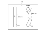
- the line width W 1 of the wiring electrode unit 120 in this specification is the line width of the wiring electrode unit 120 when the wiring electrode unit 120 is viewed from above and observed with a metal microscope or an electron microscope.
- the metal layer 121 and the conductive hard film 122 are not distinguished, and the maximum length in the width direction is used.
- the width direction of the line width W 1 as shown in FIG. 2, when viewed from the top surface of the semiconductor layer 110, the direction perpendicular to the extending direction of the wiring electrode part 120 is the width of the wiring electrode part 120 a direction, its length becomes the line width W 1.
- the line width in the length direction of the wiring of the wiring electrode part 120 is not constant, define the line width W 1 using the average value.
- the tangential direction at an arbitrary point is defined as the extending direction, and is further determined by the length in the normal direction at the arbitrary point. the width of the wiring electrode part 120 and the line width W 1.
- bent portion of the case of the broken line patterns e.g., multiple linear intersection or end points
- the line width W 1 can not be defined, from the line width in the present specification handled excluded.
- the metal layer 121 provided over the semiconductor layer 110 is a layer for forming good ohmic contact with the semiconductor layer 110, and the metal material of the metal layer 121 is appropriately selected depending on the semiconductor material of the semiconductor layer 110, the dopant, and the like. Selected.
- the metal layer 121 may have a stacked structure in which a plurality of metal materials are stacked, and may contain an alloy.
- the thickness of the metal layer 121 is generally in the range of 0.1 ⁇ m to 1 ⁇ m, and can be, for example, 0.6 to 0.9 ⁇ m.
- the metal layer 121 can form a desired wiring pattern by sequentially performing, for example, a photolithography method, an evaporation method, or a sputtering method.
- a conductive hard film 122 is provided on the metal layer 121.
- the conductive hard film 122 can also be formed with a desired wiring pattern on the metal layer 121 by sequentially performing, for example, a photolithography method, a vapor deposition method, or a sputtering method.
- the hardness of the conductive hard film 122 is higher than the hardness of the metal layer 121.
- the hardness in this specification is based on a measurement method based on the Vickers hardness defined by “JIS Z 2244 Vickers hardness test-test method—Japan Industrial Standards Committee, 2009”. It can be measured using a small hardness meter (MHA-400, manufactured by NEC).
- metal nitride can be used, and in particular, nitridation of one or more metal elements selected from the group consisting of Ti, Ta, Cr, W, Mo, and V. It can be a thing.
- metal nitrides include TiN, TaN, and WN. It is particularly preferable to use TiN having a Vickers hardness exceeding 1500 HV as the conductive hard film 122. TiN is hard and easy to handle because it is not only conductive but also has excellent wet etching characteristics.
- metal nitride instead of metal material as the material of the conductive hard film 122 is that, in the case of metal nitride, it is not only hard but also damaged without being deformed, so that the influence on local stress is made conductive. This is because the influence on the metal layer 121 can be reduced by keeping the hard film 122 damaged.
- the bonding width W 1 is 2 ⁇ m or more 5 ⁇ m or less
- the wiring electrode 120 since the bonding width between the surface of the semiconductor layer 110 (or the bonding area) is reduced, compared to when bonding width is large, It is considered that the bonding strength at the bonding surface is reduced.
- the conductive hard film 122 on the metal layer 121 peeling of the wiring electrode part 120 from the surface of the semiconductor layer 110 can be suppressed. The present inventor considers the reason that such peeling can be suppressed as follows.
- the peeling of the wiring electrode part 120 from the surface of the semiconductor layer 110 occurs when an external force in the lateral direction (transverse direction) is applied to the wiring electrode part.
- a lateral external force is generated at each stage of manufacturing, inspection, and shipment of the semiconductor optical device 100.
- a water flow for cleaning the semiconductor optical device 100, a blow (air flow) at the time of drying, adhesion to a transfer pressure-sensitive adhesive sheet, and the like can be mentioned.
- the conductive hard film 122 in this embodiment has higher hardness than the metal layer 121, the deformation of the metal layer 121 due to external force can be suppressed. Therefore, in order to reduce the force component in the direction necessary for the wiring electrode part 120 to peel from the applied external force, it is considered that the ratio of the wiring electrode part 120 that finally leads to peeling (that is, the peeling rate) is reduced. It is done.
- the peripheral portion of the wiring electrode portion 120 is not in close contact with the semiconductor layer 110, and the peripheral portion of the wiring electrode portion 120 is on the surface of the semiconductor layer 110 like a building eaves. Protrusively. If the wiring electrode part is not in close contact with the semiconductor layer 110 and has a gap, the wiring electrode part is likely to be deformed in the direction in which the force component in the direction necessary for peeling is increased if the above-described external force is present.
- the conductive hard film 122 inhibits the deformation of the wiring electrode part 120.
- the effect of the present invention that is, the suppression of peeling
- the conductive hard film 122 appears more remarkably in the semiconductor optical device 200 in which the above-described void exists.
- the “gap” between the semiconductor layer and the lower part of the periphery of the wiring electrode portion 120 is open to the outside (in other words, connected) in a direction away from the wiring electrode portion 120. It refers to a void (cavity), and voids where the space is closed are excluded.
- the thickness of the conductive hard film 122 is not limited, in order to obtain the above effect more reliably, the thickness of the conductive hard film 122 is preferably 0.4 ⁇ m or more and 1.7 ⁇ m or less, It is more preferably 0.7 ⁇ m or more and 1.5 ⁇ m or less, and most preferably 0.9 ⁇ m or more and 1.2 ⁇ m or less. This is because if the thickness is 0.4 ⁇ m or more, it is possible to reliably obtain a strength sufficient to inhibit the deformation of the wiring electrode portion 120 with respect to the external force described above.
- the conductive hard film 122 may cover the side surface of the metal layer 121, but the thickness in this case is defined by the height from the upper surface of the metal layer 121 to the upper end of the conductive hard film 122. .
- the surface of the semiconductor layer 110 may include a flat surface region F and a rough surface region R.
- the surface of the semiconductor layer 110 at the center of the junction between the surface of the semiconductor layer 110 and the wiring electrode portion 120 is a flat surface region F, and the above-described gap can be formed by the rough surface region R.
- the line width W 2 of the flat surface region F which is a bonding range between the surface of the semiconductor layer 110 and the wiring electrode unit 120, is smaller than the line width W 1 of the wiring electrode unit 120.
- a portion corresponding to [W 1 -W 2 ] is a portion where the wiring electrode portion 120 protrudes like the eaves of the building described above.
- the surface of the semiconductor layer 110 located below the peripheral edge of the wiring electrode portion 120 is a rough surface region R. That is, the surface of the semiconductor layer 110 becomes the rough surface region R in the void below the eaves at the peripheral edge of the wiring electrode portion 120.
- the line width W 1 is 2 ⁇ m or more and 5 ⁇ m or less, peeling is likely to occur. It can be remarkably suppressed.
- the gap extends to the lower part of the periphery of the metal layer 121 (that is, the metal layer It is preferable that a gap exists between the semiconductor layer 110 and the lower part of the peripheral edge 121).
- the rough surface region R of the semiconductor layer 110 extends below the periphery of the metal layer 121, for example, in order to improve the light emission output when the semiconductor optical device 100 is a light emitting element.
- region R can be confirmed by observing the cross section of the wiring electrode part 120 using a metal microscope or an electron microscope.
- the surface shape of the semiconductor layer 110 in the semiconductor optical device 200 ′ can be formed, for example, as follows. That is, first, the semiconductor layer 110 is formed by epitaxial growth by MOCVD or the like, then the metal layer 121 and the conductive hard film 122 are sequentially formed by photolithography, vapor deposition or sputtering, and the wiring electrode portion 120 is formed. Form. Thereafter, if the surface of the semiconductor layer 110 is dipped in nitric acid or the like and wet-etched, the surface of the semiconductor layer 110 infiltrates to the lower part of the peripheral portion of the wiring electrode portion 120 in addition to the exposed surface. R will be formed.
- region R provided in this way is only an example, and of course, a space
- the line width W 2 of the flat surface region F at the junction center portion between the wiring electrode portion 120 and the semiconductor layer 110 is 1.0 ⁇ m or more.
- the line width W 2 of the flat surface area F smaller than 0.5 ⁇ m than the line width W 1 of the wiring electrode part 120. That is, it is preferable that W 1 ⁇ W 2 ⁇ 0.5 ( ⁇ m). This is to increase the rough surface region R on the light emitting surface or the light receiving surface of the semiconductor optical device 200. From this viewpoint, it is more preferable that W 1 ⁇ W 2 ⁇ 1.0 ( ⁇ m).
- the semiconductor optical devices 100 and 200 can be applied to various uses.
- the semiconductor layer 110 includes a light emitting layer
- the semiconductor optical devices 100 and 200 can be semiconductor light emitting elements. More specifically, if the semiconductor layer 110 includes an n-type semiconductor layer, a light emitting layer, and a p-type semiconductor layer, and the surface of the semiconductor layer is the surface of either the n-type semiconductor layer or the p-type semiconductor layer.
- the semiconductor optical devices 100 and 200 function as semiconductor light emitting elements. If the semiconductor layer 110 includes a light receiving layer, the semiconductor optical devices 100 and 200 can be semiconductor light receiving elements or solar cells.
- the semiconductor optical device 100 may have a metal layer, an insulating layer, a reflective layer, a support substrate, and the like below the semiconductor layer 110 depending on the application.
- the method of manufacturing the semiconductor optical device 100 according to the first embodiment of the present invention includes a wiring electrode portion forming step of forming the wiring electrode portion 120 on the surface of the semiconductor layer 110 that becomes a light emitting surface or a light receiving surface.
- line width W 1 is not less 2 ⁇ m or 5 ⁇ m or less
- the wiring electrode forming step forms a first step of forming a metal layer 121 on the surface of the semiconductor layer 110, the conductive hard film 122 on the metal layer 121 A second step. It is preferable that after the wiring electrode portion forming step, a void forming step of forming a void between the lower part of the peripheral edge of the wiring electrode portion 120 and the semiconductor layer 110 is included.
- the surface of the semiconductor layer 110 is wet-etched to roughen the surface of the semiconductor layer 110 located below the peripheral edge of the wiring electrode portion 120 and to form the gap.
- the aforementioned rough surface region R can be formed.
- FIG. 4A is a cross-sectional view taken along the line II in FIG. 4B. Further, as described above, it is preferable to roughen the surface of the semiconductor layer 110 in the semiconductor optical device 200 in terms of improving the light emission efficiency, but the roughened region R is not shown in FIG. To do.
- a semiconductor light emitting device 300 includes a support substrate 180, a metal bonding layer 170 on the support substrate 180, and a metal bonding layer 170, as shown in FIGS.
- a wiring electrode part 120 including a metal layer 121 and a conductive hard film 122 provided on the surface of 111.
- the wiring electrode portion 120 is formed in the shape shown in FIG.
- a circular pad electrode 130 is provided at the center of the semiconductor light emitting device 300 on the n-type semiconductor layer 111 side.
- a lower electrode 190 may be provided on the back surface of the support substrate 180.
- the light extraction direction of the semiconductor light emitting device 300 is the wiring electrode portion 120 side (upward direction in FIG. 4A).
- Suitable materials for forming the support substrate 180 include, for example, semiconductor materials such as Si, GaAs, and Ge, metals such as Al and Cu, or alloy materials thereof, and preferably have a thickness of 100 to 300 ⁇ m. Have.
- a suitable material for forming the metal bonding layer 170 includes, for example, Au, and preferably has a thickness of 0.5 to 3.0 ⁇ m.
- the reflective layer 160 reflects the light emitted from the light emitting layer 112 toward the support substrate 180, thereby increasing the light extraction efficiency. It is desirable to have a high reflectivity with respect to the main wavelength of the light emitted from the light emitting layer 112, and it is preferable to have a reflectivity of 60% or more for light with a wavelength in the range of 300 to 1100 nm.
- a suitable material for forming the reflective layer 160 include gold (Au), aluminum (Al), silver (Ag), or an alloy containing the same as a constituent element, or a laminate thereof. It has a thickness of ⁇ 1000 nm. In general, gold (Au) or silver (Ag) has low adhesion to an insulator and easily peels off as it is.
- adhesion can be improved by interposing an adhesion layer such as Cr, Ti, or Mo.
- an adhesion layer such as Cr, Ti, or Mo.
- a thin layer of about 10 nm, for example, is used so as to transmit light.
- the ohmic electrode 140 is an electrode for forming a good ohmic contact with the p-type semiconductor layer 113.
- suitable materials constituting the ohmic electrode 140 include AuZn and AuBe, and preferably have a thickness of 100 to 500 nm.
- the insulating film 150 is not particularly limited as long as it is an insulating material that can transmit light emitted from the light emitting layer 112 and guide the light to the reflective layer 160. It is desirable to have a high transmittance with respect to the main wavelength of light emitted from the active layer, and it is preferable to have a transmittance of 80% or more for light with a wavelength in the range of 300 to 1100 nm. Suitable materials include, for example, SiN, SiO 2 and AlN, and preferably have a thickness of 100 to 500 nm.
- a suitable material for forming each layer of the semiconductor layer 110 includes a compound semiconductor, and for example, a III-V group compound semiconductor can be used.
- the III-V compound semiconductor for example, the n-type semiconductor layer 111 and the p-type semiconductor layer 113 can be made of an AlGaAs-based material, an AlGaInP-based material, an AlGaN-based material, or the like, respectively.
- the p-type impurity include Mg, Zn, and C
- examples of the n-type impurity include Si, Te, and Se.
- the light emitting layer 112 can be a single layer made of an AlGaAs-based material, an AlGaAsInP-based material, an AlGaN-based material, or a laminated structure such as a multiple quantum well. Any of these can be formed by epitaxial growth using a known method such as MOCVD.
- the emission wavelength can be in the range of 300-1100 nm.
- the thickness of each layer can be, for example, 1 to 10 ⁇ m for the n-type semiconductor layer 111, 10 to 500 nm for the light emitting layer 112, and 1 to 10 ⁇ m for the p-type semiconductor layer 113.
- the semiconductor layer 110 in which the light extraction surface side is an n-type semiconductor layer has been described so far. However, the present invention is not limited to this, and the order of p-type and n-type may be changed. Of course.
- the metal layer 121 and the conductive hard film 122 of the wiring electrode unit 120 are as described in the first embodiment.
- the metal layer 121 is an electrode for forming a good ohmic contact with the n-type semiconductor layer 111.
- a suitable material constituting such a metal layer 121 for example, AuGe, Ni, and Au are sequentially formed.
- An AuGe / Ni / Au electrode is mentioned, and preferably has a thickness of 100 to 1000 nm.
- the pad electrode 130 is a part where wire bonding is performed.
- the pad electrode 130 is provided in the central portion, but the position of the pad electrode 130 can be designed as appropriate in accordance with the wiring pattern of the wiring electrode portion 120.
- the conductive hard film 122 under the pad electrode and the conductive hard film 122 of the wiring electrode portion 120 can be formed simultaneously. In this case, although not shown, the conductive hard film 122 under the pad electrode is formed. And the height of the conductive hard film 122 of the wiring electrode portion are aligned.
- Suitable materials constituting the pad electrode 130 include Al and Au materials for fusion of Au wires on the uppermost surface, preferably a Ti / Au electrode in which Au is sequentially formed on Ti as an adhesion layer. .
- the Ti layer only needs to have a thickness that functions as an adhesion layer, and has a thickness of 50 to 200 nm.
- the Au layer preferably has a thickness of 1 to 3 ⁇ m.
- the lower electrode 190 is selected from materials that form an ohmic junction with the support substrate 180.
- materials that form an ohmic junction with the support substrate 180 For example, when n-type GaAs is selected as the support substrate, a laminate of AuGe / Ni / Au or the like can be selected.
- a metal substrate is used as the support substrate 180, a structure without a lower electrode can be selected.
- the light-transmitting insulating layer on the semiconductor layer 110 and the light-transmitting insulating layer are provided below the pad electrode 130 and between the semiconductor layer 110 and the conductive hard film 122. It is also preferable to provide an upper reflective layer.
- the translucent insulating layer functions as a current blocking layer. In this case, an opening is provided in the metal layer 121 below the pad electrode 130, and the metal layer 121 can be disposed so as to surround the light-transmitting insulating layer and the reflective layer.
- the light-transmitting insulating layer is preferably a material having a transmittance of 80% or more with respect to light having a wavelength in the range of 300 to 1100 nm.
- suitable materials include SiN, SiO 2 , and AlN. And preferably has a thickness of 100 to 500 nm.
- the reflective layer is preferable because it can reflect the light traveling from the light emitting layer 112 toward the pad electrode 130 to increase the light extraction efficiency.
- Suitable materials for forming the reflective layer include, for example, gold (Au) or a gold alloy material, platinum (Pt), aluminum (Al), silver (Ag) alone or an alloy containing the same as a constituent element, or a laminate thereof.
- Au gold
- Pt platinum
- Al aluminum
- Ag silver
- a Cr / Au electrode in which Au showing a reflectance of 90% or more in the same region is disposed through a thin adhesion layer of Cr is used.
- the Cr layer as the adhesion material has a thickness of 5 to 20 nm
- the Au layer as the reflection material has a thickness of 100 to 1000 nm.
- the light-transmitting insulating layer and the reflective layer can be formed by a photolithography method and a sputtering method, a plasma CVD method, an electron beam evaporation method, a resistance heating evaporation method, or the like.
- the film thickness measurement method in this specification is based on a stylus-type step gauge, and the five points in the wafer surface (in the case of the 3-inch substrate of the present embodiment, on the diagonal line passing through the wafer center, The average value of the measurement of 5 points at an equal distance with 2 points inside 1 cm from the two ends.
- a semiconductor layer 110 is formed on a growth substrate G such as a GaAs substrate.
- the semiconductor layer 110 is formed by epitaxially growing an n-type semiconductor layer 111, a light emitting layer 112, and a p-type semiconductor layer 113 made of the materials described above in this order, for example, by MOCVD.
- an ohmic electrode 140 having a predetermined pattern is formed on the semiconductor layer 110.
- a material as described above is deposited by resistance heating vapor deposition or electron beam vapor deposition, a resist pattern is formed by photolithography, and then etched to form a predetermined pattern, and then contact annealing (RTA: Rapid Thermal Annealing).
- RTA Rapid Thermal Annealing
- the insulating film 150 is formed over the semiconductor layer 110 where the ohmic electrode is not formed. This can be obtained, for example, by forming a material as described above by a plasma CVD method or a sputtering method.
- a resist pattern in which only ohmic electrodes are opened is formed by photolithography, and an opening for energization is formed in the insulating film by wet etching the insulating film with a predetermined etching solution.
- the reflective layer 160 is formed by, for example, sputtering.
- Au or the like is formed as a first metal bonding layer 170a (semiconductor layer side bonding layer) by a method such as vapor deposition.
- the substrate shown in (1) is bonded.
- the first metal bonding layer 170a and the second metal bonding layer 170b are bonded and heated, whereby the two substrates are bonded to each other at the metal bonding layer 170.
- the formation of the second metal bonding layer 170b on the support substrate 180 can be performed by a method similar to that for the first metal bonding layer 170a.
- the lower electrode 190 is formed on the support substrate 180 by depositing the above-described material by, for example, a sputtering method or an electron beam evaporation method.
- the lower electrode 190 may be formed after the pad electrode 130 described later is formed.
- the growth substrate G is ground and further etched to remove the growth substrate G.
- a metal layer 121 having a predetermined wiring pattern is formed on the semiconductor layer 110.
- a material as described above is formed by, for example, a resistance heating vapor deposition method, a resist pattern is formed by photolithography, etched to form a predetermined pattern, and then contact annealing (RTA: Rapid Thermal Annealing).
- RTA Rapid Thermal Annealing
- deposition by resistance heating is a method of vapor deposition by heating and evaporating a metal in a vacuum, and in order to heat the vapor deposition metal, a base of a high melting point material on which the vapor deposition metal is placed. It is a method of energizing (for example, a tungsten wire or a boat) to increase the temperature by heat generated by metal resistance.
- a conductive hard film 122 is formed on the metal layer 121.
- a resist pattern is formed by photolithography, and the conductive hard film 122 is formed by a sputtering method or the like.
- the pad electrode 130 may be formed at a predetermined position on the conductive hard film 122 by, for example, sputtering, electron beam evaporation, or evaporation by resistance heating. In this case, after the film formation, the conductive hard film and the pad electrode where the resist is left may be removed by lift-off.
- the surface of the semiconductor layer 110 is roughened by performing wet etching by dipping in nitric acid or the like.
- the line width W 2 of the above with reference to FIG. 3, can be adjusted kind of the etchant, the etching time or the like.
- an LED element using the semiconductor light emitting element 400 can be manufactured.
- the semiconductor light emitting elements 300 and 400 which are wafer bonded LED elements and the manufacturing method thereof have been described, but the present invention is limited to the wafer bonded LED elements. Absent.
- all of the above-described examples show examples of typical embodiments, and the present invention is not limited to these embodiments.
- the semiconductor light emitting elements 300 and 400 are only specific examples of the semiconductor optical devices 100 and 200, and those skilled in the art can apply the semiconductor optical devices 100 and 200 to semiconductor light receiving elements and solar cells. Naturally understood.
- a semiconductor light emitting device as a semiconductor optical device according to the present invention was manufactured by the method shown in FIG. First, an n-type semiconductor layer (thickness: 7.5 ⁇ m, AlGaAs material), a light-emitting layer (total thickness: 50 nm, AlGaInAs material) and a p-type semiconductor layer (thickness) are formed on a growth substrate made of a GaAs material by MOCVD. A semiconductor layer made of 2 ⁇ m AlGaAs material) was formed.
- AuZn (thickness: 200 nm) was formed on the p-type semiconductor layer by a resistance heating vapor deposition method, patterned by photolithography, and contact annealed at 420 ° C. to form an ohmic electrode. Thereafter, a transparent insulating film made of SiO 2 was formed by plasma CVD on the p-type semiconductor layer where the ohmic electrode was not formed. Thereafter, a reflective layer (thickness: 750 nm, Au material) was formed by electron beam evaporation. Furthermore, Ti / Au (thickness: 100 nm / 1 ⁇ m) was formed by vapor deposition as the semiconductor layer side bonding layer.
- an ohmic electrode (thickness: 200 nm, AuGe / Ni / Au material) is formed on one side of a support substrate made of a GaAs material by vapor deposition by resistance heating, and Ti / Au is used as a support substrate side bonding layer. (Thickness: 100 nm / 1 ⁇ m) was formed by electron beam evaporation. And the semiconductor layer side joining layer and the support substrate side joining layer were adhere
- an etching solution comprising ammonia, hydrogen peroxide solution, and water.
- a resist is formed on the n-type semiconductor layer exposed by removing the growth substrate at a position other than the wiring pattern of FIG. 4B by photolithography, and AuGe / Ni / Au (total thickness: 0. 0).
- the metal layer 121 having the wiring pattern shown in FIG. 4B was formed by lift-off for removing the resist.
- the line width of the metal layer 121 (that is, the line width W 1 of the wiring electrode portion) was set to 4.0 ⁇ m.
- a resist is formed again at a position other than the wiring pattern in FIG.
- a resist pattern was formed at a position other than the central portion of FIG. 4B by photolithography, and a pad electrode (thickness: 100 nm / 1.5 ⁇ m, Ti / Au material) was formed by an electron beam evaporation method. . And the pad electrode was formed using the lift-off method which removes a resist.
- a mesa pattern was formed by etching with a mixed solution of phosphoric acid and hydrogen peroxide solution.
- Invention Example 2 A semiconductor light emitting device according to Invention Example 2 was produced in the same manner as Invention Example 1, except that the thickness of the conductive hard film in Invention Example 1 was changed from 0.9 ⁇ m to 0.5 ⁇ m.
- Invention Example 3 A semiconductor light emitting device according to Invention Example 3 was produced in the same manner as Invention Example 1, except that the thickness of the conductive hard film in Invention Example 1 was changed from 0.9 ⁇ m to 1.5 ⁇ m.
- Comparative Example 1 A semiconductor light emitting device according to Comparative Example 1 was fabricated in the same manner as Invention Example 1 except that the thickness of the conductive hard film in Invention Example 1 was changed from 0.9 ⁇ m to 1.9 ⁇ m.
- Comparative Example 2 A semiconductor light emitting device according to Comparative Example 3 was produced in the same manner as in Invention Example 1 except that the conductive hard film formed in Invention Example 1 was not formed.
- Table 1 shows the manufacturing conditions of the above Invention Examples 1 to 3, Comparative Examples 1 and 2, and Conventional Examples 1 and 2. Table 1 also shows the evaluation results described later.
- FIG. 6 shows a photomicrograph of the semiconductor light emitting device of Example 1 that was determined not to peel.
- Comparative Example 2 can improve the light emission output, the wiring electrode portion has a high peeling rate and cannot withstand commercialization. Compared to Comparative Example 2, it was confirmed that the peeling rates could be reduced in Invention Examples 1 to 3 provided with a conductive hard film. In Comparative Example 1 in which the thickness of the conductive hard film was 1.9 ⁇ m, the peel rate was high as in Comparative Example 2. It is presumed that this is because the thickness of the wiring electrode portion is 0.8 ⁇ m, and the thickness of the conductive hard film is set to an extreme thickness that is twice or more.
- the present invention it is possible to provide a semiconductor optical device having a light extraction efficiency or light capturing efficiency superior to that of the prior art, and having a reduced peeling rate of the wiring electrode portion, and a manufacturing method thereof, which is useful.
- SYMBOLS 100, 200 Semiconductor optical device 300, 400 Semiconductor light emitting element 110 Semiconductor layer 111 N type semiconductor layer 112 Light emitting layer 113 P type semiconductor layer 120 Wiring electrode part 121 Metal layer 122 Conductive hard film 130 Pad electrode 140 Ohmic electrode 150 Insulating film 160 Reflective layer 170 Metal bonding layer 180 Support substrate 190 Lower electrode G Growth substrate F Flat surface region R Rough surface region
Landscapes
- Led Devices (AREA)
- Light Receiving Elements (AREA)
Abstract
L'invention concerne un dispositif optique à semi-conducteurs présentant un taux de pelage réduit d'une section d'électrode de câblage, tout en présentant un rendement d'extraction de lumière élevé ou un rendement d'admission de lumière élevé par comparaison avec des dispositifs conventionnels ; et un procédé pour la fabrication du dispositif à semi-conducteurs. La présente invention concerne un dispositif optique à semi-conducteurs dans lequel : une section d'électrode de câblage 120 est prévue sur la surface avant d'une couche conductrice 110, ladite surface avant étant prévue pour être une surface d'émission de lumière ou une surface de réception de lumière ; la largeur de ligne W1 de la section d'électrode de câblage 120 est comprise entre 2-5 µm ; la section d'électrode de câblage 120 présente une couche métallique 121 sur la couche semi-conductrice 110, et un film dur conducteur 122 sur la couche métallique 121 ; et le film dur conducteur 122 présente une dureté supérieure à celle de la couche métallique 121.<sb />
Priority Applications (2)
| Application Number | Priority Date | Filing Date | Title |
|---|---|---|---|
| US16/080,395 US10658543B2 (en) | 2016-03-11 | 2017-01-30 | Semiconductor optical device and method of manufacturing the same |
| CN201780016697.3A CN108780824B (zh) | 2016-03-11 | 2017-01-30 | 半导体光器件和其制造方法 |
Applications Claiming Priority (2)
| Application Number | Priority Date | Filing Date | Title |
|---|---|---|---|
| JP2016-048820 | 2016-03-11 | ||
| JP2016048820A JP6738169B2 (ja) | 2016-03-11 | 2016-03-11 | 半導体光デバイスおよびその製造方法 |
Publications (1)
| Publication Number | Publication Date |
|---|---|
| WO2017154404A1 true WO2017154404A1 (fr) | 2017-09-14 |
Family
ID=59789160
Family Applications (1)
| Application Number | Title | Priority Date | Filing Date |
|---|---|---|---|
| PCT/JP2017/003190 Ceased WO2017154404A1 (fr) | 2016-03-11 | 2017-01-30 | Dispositif optique à semi-conducteurs et procédé pour sa fabrication |
Country Status (4)
| Country | Link |
|---|---|
| US (1) | US10658543B2 (fr) |
| JP (1) | JP6738169B2 (fr) |
| CN (1) | CN108780824B (fr) |
| WO (1) | WO2017154404A1 (fr) |
Families Citing this family (2)
| Publication number | Priority date | Publication date | Assignee | Title |
|---|---|---|---|---|
| JP7138517B2 (ja) * | 2017-10-18 | 2022-09-16 | ローム株式会社 | 半導体発光装置 |
| JP7160781B2 (ja) * | 2019-10-31 | 2022-10-25 | Dowaエレクトロニクス株式会社 | 発光素子及びその製造方法 |
Citations (6)
| Publication number | Priority date | Publication date | Assignee | Title |
|---|---|---|---|---|
| JP2006245379A (ja) * | 2005-03-04 | 2006-09-14 | Stanley Electric Co Ltd | 半導体発光素子 |
| JP2008288548A (ja) * | 2007-04-16 | 2008-11-27 | Toyoda Gosei Co Ltd | 半導体発光素子 |
| JP2011066453A (ja) * | 2010-12-27 | 2011-03-31 | Toshiba Corp | 半導体発光素子及び半導体発光装置 |
| WO2012120894A1 (fr) * | 2011-03-10 | 2012-09-13 | Dowaエレクトロニクス株式会社 | Élément électroluminescent semi-conducteur, et procédé de fabrication associé |
| JP2013211595A (ja) * | 2007-12-28 | 2013-10-10 | Nichia Chem Ind Ltd | 半導体発光素子の製造方法 |
| JP2015204333A (ja) * | 2014-04-11 | 2015-11-16 | 豊田合成株式会社 | 半導体装置および半導体装置の製造方法 |
Family Cites Families (22)
| Publication number | Priority date | Publication date | Assignee | Title |
|---|---|---|---|---|
| US6066516A (en) * | 1995-06-26 | 2000-05-23 | Seiko Epson Corporation | Method for forming crystalline semiconductor layers, a method for fabricating thin film transistors, and method for fabricating solar cells and active matrix liquid crystal devices |
| JP2959493B2 (ja) * | 1996-10-25 | 1999-10-06 | サンケン電気株式会社 | 半導体発光素子 |
| JP2959503B2 (ja) * | 1997-01-10 | 1999-10-06 | サンケン電気株式会社 | 半導体発光素子 |
| JP3156756B2 (ja) * | 1997-01-10 | 2001-04-16 | サンケン電気株式会社 | 半導体発光素子 |
| JP3648397B2 (ja) * | 1998-12-28 | 2005-05-18 | シャープ株式会社 | 化合物半導体装置の電極構造 |
| JP3654059B2 (ja) | 1999-06-25 | 2005-06-02 | 松下電工株式会社 | 赤外線センサーの製造方法 |
| JP2003008055A (ja) * | 2001-06-20 | 2003-01-10 | Daido Steel Co Ltd | 半導体発光素子の製造方法 |
| JP4547933B2 (ja) * | 2003-02-19 | 2010-09-22 | 日亜化学工業株式会社 | 窒化物半導体素子 |
| JP4597653B2 (ja) * | 2004-12-16 | 2010-12-15 | 住友電工デバイス・イノベーション株式会社 | 半導体装置、それを備える半導体モジュールおよび半導体装置の製造方法。 |
| JP2006253298A (ja) * | 2005-03-09 | 2006-09-21 | Toshiba Corp | 半導体発光素子及び半導体発光装置 |
| JP4449919B2 (ja) * | 2006-02-16 | 2010-04-14 | 住友電気工業株式会社 | 発光装置の製造方法 |
| JP2007258326A (ja) | 2006-03-22 | 2007-10-04 | Matsushita Electric Ind Co Ltd | 発光素子 |
| JP5192163B2 (ja) * | 2007-03-23 | 2013-05-08 | 住友電工デバイス・イノベーション株式会社 | 半導体装置 |
| JP2011100829A (ja) | 2009-11-05 | 2011-05-19 | Toshiba Corp | 半導体発光装置の製造方法および半導体発光装置 |
| KR101014155B1 (ko) * | 2010-03-10 | 2011-02-10 | 엘지이노텍 주식회사 | 발광 소자, 발광 소자 제조방법 및 발광 소자 패키지 |
| JP5095785B2 (ja) * | 2010-08-09 | 2012-12-12 | 株式会社東芝 | 半導体発光素子及びその製造方法 |
| CN103222074B (zh) * | 2010-11-18 | 2016-06-01 | 首尔伟傲世有限公司 | 具有电极焊盘的发光二极管芯片 |
| JP4989773B1 (ja) * | 2011-05-16 | 2012-08-01 | 株式会社東芝 | 半導体発光素子 |
| US8884157B2 (en) * | 2012-05-11 | 2014-11-11 | Epistar Corporation | Method for manufacturing optoelectronic devices |
| EP2903007B1 (fr) * | 2012-09-25 | 2019-05-08 | National Institute of Advanced Industrial Science and Technology | Procédé de formation de motifs |
| JP6330125B2 (ja) * | 2013-11-28 | 2018-05-30 | 株式会社ムラカミ | 太陽電池の製造方法 |
| TWI710144B (zh) * | 2015-02-17 | 2020-11-11 | 新世紀光電股份有限公司 | 具布拉格反射鏡之發光二極體及其製造方法 |
-
2016
- 2016-03-11 JP JP2016048820A patent/JP6738169B2/ja active Active
-
2017
- 2017-01-30 WO PCT/JP2017/003190 patent/WO2017154404A1/fr not_active Ceased
- 2017-01-30 US US16/080,395 patent/US10658543B2/en active Active
- 2017-01-30 CN CN201780016697.3A patent/CN108780824B/zh active Active
Patent Citations (6)
| Publication number | Priority date | Publication date | Assignee | Title |
|---|---|---|---|---|
| JP2006245379A (ja) * | 2005-03-04 | 2006-09-14 | Stanley Electric Co Ltd | 半導体発光素子 |
| JP2008288548A (ja) * | 2007-04-16 | 2008-11-27 | Toyoda Gosei Co Ltd | 半導体発光素子 |
| JP2013211595A (ja) * | 2007-12-28 | 2013-10-10 | Nichia Chem Ind Ltd | 半導体発光素子の製造方法 |
| JP2011066453A (ja) * | 2010-12-27 | 2011-03-31 | Toshiba Corp | 半導体発光素子及び半導体発光装置 |
| WO2012120894A1 (fr) * | 2011-03-10 | 2012-09-13 | Dowaエレクトロニクス株式会社 | Élément électroluminescent semi-conducteur, et procédé de fabrication associé |
| JP2015204333A (ja) * | 2014-04-11 | 2015-11-16 | 豊田合成株式会社 | 半導体装置および半導体装置の製造方法 |
Also Published As
| Publication number | Publication date |
|---|---|
| US20190273182A1 (en) | 2019-09-05 |
| JP6738169B2 (ja) | 2020-08-12 |
| CN108780824B (zh) | 2021-09-24 |
| CN108780824A (zh) | 2018-11-09 |
| JP2017163111A (ja) | 2017-09-14 |
| US10658543B2 (en) | 2020-05-19 |
Similar Documents
| Publication | Publication Date | Title |
|---|---|---|
| JP5779642B2 (ja) | 半導体発光素子およびその製造方法 | |
| JP5883118B2 (ja) | オプトエレクトロニクス半導体チップ | |
| EP1821346A2 (fr) | Dispositif électroluminescent semi-conducteur et son procédé de fabrication | |
| JP5630384B2 (ja) | Iii族窒化物半導体発光素子の製造方法 | |
| JP5639626B2 (ja) | 半導体発光素子及び電極成膜方法 | |
| WO2010073883A1 (fr) | Elément électroluminescent semi-conducteur | |
| WO2011018942A1 (fr) | Elément électroluminescent semi-conducteur, dispositif électroluminescent semi-conducteur, procédé de production délément électroluminescent semi-conducteur, procédé de production de dispositif électroluminescent semi-conducteur, dispositif déclairage faisant appel au dispositif électroluminescent semi-conducteur, et appareil électronique | |
| KR101161897B1 (ko) | 질화물 반도체 소자 | |
| TWI222759B (en) | Light emitting diode and method for manufacturing the same | |
| WO2010071113A1 (fr) | Élément électroluminescent à semi-conducteur | |
| JP2004207508A (ja) | 発光素子及びその製造方法 | |
| JP2016134422A (ja) | 半導体発光素子およびその製造方法 | |
| JP6040769B2 (ja) | 発光素子及びその製造方法 | |
| CN102460743A (zh) | 发光半导体器件及其制造方法 | |
| JP6738169B2 (ja) | 半導体光デバイスおよびその製造方法 | |
| JP2012084779A (ja) | 半導体発光素子 | |
| US8785219B1 (en) | Optoelectronic semiconductor device and the manufacturing method thereof | |
| JP6119906B2 (ja) | 発光素子 | |
| JP2009094108A (ja) | GaN系LED素子の製造方法 | |
| CN114725263B (zh) | 一种低阻高反射欧姆接触电极及其制备方法 | |
| WO2005109530A1 (fr) | Dispositif électroluminescent semi-conducteur et procédé de fabrication dudit dispositif | |
| JP2012104730A (ja) | 半導体発光素子 | |
| TW202228306A (zh) | 紅外led元件 | |
| JP2024106499A (ja) | 赤外led素子 | |
| JP2012069683A (ja) | 発光素子 |
Legal Events
| Date | Code | Title | Description |
|---|---|---|---|
| NENP | Non-entry into the national phase |
Ref country code: DE |
|
| 121 | Ep: the epo has been informed by wipo that ep was designated in this application |
Ref document number: 17762750 Country of ref document: EP Kind code of ref document: A1 |
|
| 122 | Ep: pct application non-entry in european phase |
Ref document number: 17762750 Country of ref document: EP Kind code of ref document: A1 |