WO2017154541A1 - Réceptacle optique et module optique - Google Patents
Réceptacle optique et module optique Download PDFInfo
- Publication number
- WO2017154541A1 WO2017154541A1 PCT/JP2017/006138 JP2017006138W WO2017154541A1 WO 2017154541 A1 WO2017154541 A1 WO 2017154541A1 JP 2017006138 W JP2017006138 W JP 2017006138W WO 2017154541 A1 WO2017154541 A1 WO 2017154541A1
- Authority
- WO
- WIPO (PCT)
- Prior art keywords
- optical
- light
- optical receptacle
- receptacle
- emitted
- Prior art date
- Legal status (The legal status is an assumption and is not a legal conclusion. Google has not performed a legal analysis and makes no representation as to the accuracy of the status listed.)
- Ceased
Links
Images


Classifications
-
- G—PHYSICS
- G02—OPTICS
- G02B—OPTICAL ELEMENTS, SYSTEMS OR APPARATUS
- G02B6/00—Light guides; Structural details of arrangements comprising light guides and other optical elements, e.g. couplings
- G02B6/24—Coupling light guides
- G02B6/42—Coupling light guides with opto-electronic elements
- G02B6/4201—Packages, e.g. shape, construction, internal or external details
- G02B6/4204—Packages, e.g. shape, construction, internal or external details the coupling comprising intermediate optical elements, e.g. lenses, holograms
- G02B6/4206—Optical features
-
- G—PHYSICS
- G02—OPTICS
- G02B—OPTICAL ELEMENTS, SYSTEMS OR APPARATUS
- G02B6/00—Light guides; Structural details of arrangements comprising light guides and other optical elements, e.g. couplings
- G02B6/24—Coupling light guides
- G02B6/42—Coupling light guides with opto-electronic elements
-
- G—PHYSICS
- G02—OPTICS
- G02B—OPTICAL ELEMENTS, SYSTEMS OR APPARATUS
- G02B6/00—Light guides; Structural details of arrangements comprising light guides and other optical elements, e.g. couplings
- G02B6/24—Coupling light guides
- G02B6/42—Coupling light guides with opto-electronic elements
- G02B6/4201—Packages, e.g. shape, construction, internal or external details
- G02B6/4204—Packages, e.g. shape, construction, internal or external details the coupling comprising intermediate optical elements, e.g. lenses, holograms
- G02B6/4214—Packages, e.g. shape, construction, internal or external details the coupling comprising intermediate optical elements, e.g. lenses, holograms the intermediate optical element having redirecting reflective means, e.g. mirrors, prisms for deflecting the radiation from horizontal to down- or upward direction toward a device
-
- G—PHYSICS
- G02—OPTICS
- G02B—OPTICAL ELEMENTS, SYSTEMS OR APPARATUS
- G02B6/00—Light guides; Structural details of arrangements comprising light guides and other optical elements, e.g. couplings
- G02B6/24—Coupling light guides
- G02B6/42—Coupling light guides with opto-electronic elements
- G02B6/4201—Packages, e.g. shape, construction, internal or external details
- G02B6/4246—Bidirectionally operating package structures
Definitions
- the present invention relates to an optical receptacle and an optical module having the optical receptacle.
- an optical module including a photoelectric conversion element (light emitting element, light receiving element or both) is used for optical communication using an optical transmission body such as an optical fiber or an optical waveguide.
- an optical receptacle is used that is disposed between the photoelectric conversion element and the optical transmission body and optically couples the photoelectric conversion element and the end face of the optical transmission body.
- Optical modules include a transmission optical module having a transmission function, a reception optical module having a reception function, and a transmission / reception optical module having a transmission function and a reception function.
- an optical filter for attenuating the intensity of light emitted from the optical receptacle may be used (for example, see Patent Document 1).
- FIG. 1 is a cross-sectional view showing a configuration of an optical receptacle 1 described in Patent Document 1.
- An optical receptacle 1 described in Patent Document 1 includes an optical receptacle body 2 and an optical filter 3 (for example, an optical attenuation filter).
- the optical receptacle body 2 includes a lens surface 4 arranged in a line at equal intervals on the bottom surface of the optical receptacle body 2, and an optical surface 5 arranged on the opposite side of the lens surface 4. And have.
- the optical filter 3 is disposed on a part of the optical surface 5.
- a photoelectric conversion device having a plurality of light emitting elements and a plurality of light receiving elements is arranged on the lens surface 4 side, and a plurality of optical transmission bodies are arranged on the optical surface 5 side. Used in.
- the optical receptacle 1 described in Patent Document 1 since the optical filter 3 is disposed on the optical path of the light emitted from the light emitting element and incident on the optical transmission body, the optical receptacle 1 is emitted from the optical receptacle 1 toward the optical transmission body. The intensity of light can be attenuated.
- the optical receptacle 1 described in Patent Document 1 is optically applied to a portion that functions as an optical module for reception.
- the filter 3 may be applied, and the intensity of light emitted from the end face of the optical transmission body toward the optical receptacle 1 may be attenuated.
- a first object of the present invention is to provide an optical receptacle capable of appropriately attenuating only the intensity of light passing through a transmission portion even though it includes a transmission portion and a reception portion.
- the second object of the present invention is to provide an optical module having the optical receptacle.
- An optical receptacle according to the present invention is disposed between a photoelectric conversion device in which a light emitting element and a light receiving element are disposed on a substrate and a plurality of optical transmission bodies, and the light emitting element, the light receiving element, and the plurality of lights.
- a first optical receptacle for transmission disposed on the substrate so as to face the light emitting element, and a second side surface different from a surface facing the substrate, wherein the first or two or more first optical receptacles are disposed.
- a second optical receptacle for reception that has one or two or more second fitting portions fitted to the fitting portion and is disposed on the substrate so as to face the light receiving element; Incident light incident on the first optical receptacle.
- the proportion of the intensity of the outgoing light emitted from the first optical receptacle for degree of which is smaller than the ratio of the intensity of emitted light emitted from said second optical receptacle to the intensity of light incident on the second optical receptacle.
- An optical module includes a substrate, a photoelectric conversion device having a light emitting element and a light receiving element disposed on the substrate, and an optical receptacle according to the present invention, wherein the first optical receptacle is The second optical receptacle is disposed on the substrate so as to face the light emitting element, and the second optical receptacle is disposed on the substrate so as to face the light receiving element.
- the first optical receptacle and the first optical receptacle The two-light receptacle is connected to each other by fitting the first fitting portion and the second fitting portion.
- the transmission part and the reception part of the optical receptacle are manufactured separately, only the intensity of light passing through the transmission part is adequate even if the transmission part and the reception part are included. Can be attenuated.
- FIG. 1 is a cross-sectional view showing a configuration of an optical receptacle described in Patent Document 1.
- FIG. 2A and 2B are diagrams schematically showing the configuration of the optical module according to Embodiment 1.
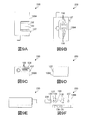
- FIG. 3A to 3F are diagrams showing the configuration of the optical receptacle according to the first embodiment.
- 4A to 4F are diagrams showing the configuration of the first optical receptacle according to Embodiment 1.
- FIG. 5A and 5B are diagrams showing the configuration of the light separating section of the first optical receptacle according to Embodiment 1.
- FIG. 6A to 6F are diagrams showing the configuration of the second optical receptacle according to the first embodiment.
- FIG. 7A and 7B are diagrams schematically illustrating the configuration of the optical module according to Embodiment 2.
- FIG. 8A to 8F are diagrams showing the configuration of the optical receptacle according to the second embodiment.
- 9A to 9F are diagrams showing the configuration of the first optical receptacle according to the second embodiment.
- FIGS. 2A and 2B are diagrams schematically showing the configuration of the optical module 100 according to Embodiment 1 of the present invention.
- 2A is a cross-sectional view taken along line AA in FIG. 3B described later
- FIG. 2B is a cross-sectional view taken along line BB in FIG. 3B described later.
- the cross section of the optical receptacle 120 is not hatched in order to show the optical path in the optical receptacle 120.
- the alternate long and short dash line indicates the optical axis of light
- the broken line indicates the outer diameter of light.
- the optical module 100 includes a photoelectric conversion device 110 and an optical receptacle 120.
- the optical module 100 according to the present embodiment is a transmission / reception optical module.
- FIG. 2A shows a part that functions as a transmission optical module
- FIG. 2B shows a part that functions as a reception optical module. Is shown.
- the optical module 100 is used in a state where the optical transmission body 150 is connected to the optical receptacle 120.
- the photoelectric conversion device 110 includes a substrate 111, a light emitting element 112, a detecting element 113, a light receiving element 114, and a control unit (not shown).
- the substrate 111 holds the light emitting element 112, the detecting element 113, the light receiving element 114, the control unit, and the optical receptacle 120.
- the substrate 111 is, for example, a glass composite substrate, a glass epoxy substrate, or a flexible sill substrate.
- the light emitting element 112 is disposed on the substrate 111.
- the light emitting element 112 is disposed in a portion that functions as an optical module for transmission.
- the number and position of the light emitting elements 112 are not particularly limited, and can be set as appropriate according to the application. In the present embodiment, four light emitting elements are arranged on the same straight line along a direction perpendicular to the paper surface of FIGS. 2A and 2B.
- the light emitting element emits laser light in a direction perpendicular to the surface of the substrate 111. More specifically, the light emitting element emits laser light from a light emitting surface (light emitting region).
- the number and position of the light emitting elements are not particularly limited.
- the light emitting element is, for example, a vertical cavity surface emitting laser (VCSEL).
- the detection element 113 is disposed on the substrate 111, and monitors the first emitted light L1 emitted from the light emitting surface (light emitting region) of the light emitting element 112. Specifically, the detection element 113 receives the monitor light Lm that is a part of the first emitted light emitted from the optical receptacle 120.
- the detection element 113 is, for example, a photodiode (PD).
- the number of detection elements 113 is not particularly limited, and can be set as appropriate according to the application. In the present embodiment, the number of detection elements 113 is the same as the number of light emitting elements, and is four. The four detection elements 113 are arranged at positions where the monitor light Lm on the substrate 111 can be received. Further, from the viewpoint of preventing the reflected light from the detection element 113 from returning into the optical receptacle 120 (first optical receptacle 130 described later), the optical axis of the monitor light Lm incident on the detection element 113 is You may incline with respect to a detection surface.
- the light receiving element 114 is disposed on the substrate 111.
- the light receiving element 114 is disposed in a portion that functions as a receiving optical module.
- the number and position of the light receiving elements 114 are not particularly limited, and can be set as appropriate according to the application. In the present embodiment, four light receiving elements 114 are arranged on the same straight line along a direction perpendicular to the paper surface of FIGS. 2A and 2B.
- the light receiving element 114 receives light (second emission light L2 described later) emitted from the end face of the optical transmission body 150 and passed through the inside of the optical receptacle 120 (second optical receptacle 140 described later). More specifically, the light receiving element 114 receives the second emitted light L2 at the light receiving surface (light receiving region).
- the light receiving element 114 is, for example, a photodiode (PD).
- control unit is disposed on the substrate 111 and is electrically connected to the light emitting element 112 and the detection element 113 via wiring.
- the control unit controls the output of the first emitted light L1 emitted from the light emitting element 112 based on the intensity or the light amount of the monitor light Lm received by the detection element 113.
- the optical receptacle 120 is disposed between the light emitting element 112 and the light receiving element 114 and the plurality of light transmission bodies 150, and the light receptacle 120 and the light receiving element 114 and the end faces of the plurality of light transmission bodies 150 are Each is optically coupled.
- the optical receptacle 120 receives the signal light Ls, which is a part of the first emitted light L1 emitted from the light emitting element 112, as the optical transmission body 150. The light is emitted toward the end face of.
- the optical receptacle 120 (second optical receptacle 140) emits the second emitted light L ⁇ b> 2 emitted from the end face of the optical transmission body 150 toward the light receiving element 114.
- the optical receptacle 120 will be described in detail separately, but here, the name of light in this specification will be described.
- 2A shows light (L1, Ls, and Lm) that passes through a portion that functions as an optical module for transmission
- FIG. 2B shows light (L2) that passes through a portion that functions as an optical module for reception. It is shown.
- the light emitted from the light emitting element 112 is referred to as “first emitted light L1”.
- the first emitted light L1 means light from the light emitting surface of the light emitting element 112 until it reaches a light separating unit 133 described later.
- a part of the first emitted light L1 which is separated by the light separation unit 133 and emitted from the optical receptacle 120 (first optical receptacle 130) toward the end face of the optical transmission body 150, is “ This is referred to as “signal light Ls”.
- the signal light Ls means light from the light separation unit 133 until it reaches the end face of the optical transmission body 150.
- the other part of the first emitted light L1 which is separated by the light separation unit 133 and emitted from the optical receptacle 120 (first optical receptacle 130) toward the detection element 113, is referred to as “monitor light Lm”. ". That is, the monitor light Lm means light from the light separation unit 133 until it reaches the detection element 113. Furthermore, the light emitted from the end face of the optical transmission body 150 is referred to as “second emitted light L2”. The second outgoing light L2 means light from the end face of the optical transmission body 150 to the light receiving surface of the light receiving element 114. The second emitted light L2 is also received light emitted from another optical module.
- the photoelectric conversion device 110 and the optical receptacle 120 are fixed to each other by known fixing means such as an adhesive (for example, heat / ultraviolet curable resin).
- the optical transmission body 150 is attached to the optical receptacle 120 through known attachment means in a state of being accommodated in a multi-core batch type connector.
- the type of the optical transmission body 150 is not particularly limited. Examples of types of the optical transmission body 150 include an optical fiber and an optical waveguide.
- the optical transmission body 150 is an optical fiber.
- the optical fiber may be a single mode method or a multi mode method.
- the number of optical transmission bodies 150 is not particularly limited, and can be changed as appropriate according to the application. In the present embodiment, the number of optical transmission bodies 150 is eight. Four eight optical transmission bodies 150 are arranged in each of a part functioning as a transmission optical module and a part functioning as a reception optical module of the optical module 100.
- FIGS. 3A to 3F are diagrams showing the configuration of the optical receptacle 120 according to the present embodiment.
- 3A is a plan view of the optical receptacle 120
- FIG. 3B is a bottom view
- FIG. 3C is a front view
- FIG. 3D is a rear view
- FIG. 3E is a left side view
- FIG. 3F is a right side view.
- the surface on the side to which the optical transmission body 150 is connected is described as the “front surface” of the optical receptacle 120.
- the optical receptacle 120 includes a first optical receptacle 130 for transmission and a second optical receptacle 140 for reception.
- the first optical receptacle 130 and the second optical receptacle 140 are connected to each other by fitting a first fitting portion 137 and a second fitting portion 144 described later.
- the first optical receptacle 130 is disposed on the substrate 111 so as to face the light emitting element 112 and the detection element 113.
- the first optical receptacle 130 causes the first emitted light L1 emitted from the light emitting element 112 to enter the first optical receptacle 130, and emits the signal light Ls and the monitor light Lm to the outside of the first optical receptacle 130.
- the second optical receptacle 140 is disposed on the substrate 111 so as to face the light receiving element 114.
- the second optical receptacle 140 causes the second emitted light L2 emitted from the end face of the optical transmission body 150 to enter the second optical receptacle 140, and causes the second emitted light L2 to be emitted outside the second optical receptacle 140.
- the intensity of the outgoing light emitted from the first optical receptacle 130 relative to the intensity of the incident light (first outgoing light L1 in this embodiment) incident on the first optical receptacle 130 (in this embodiment, the signal light Ls
- the first transmittance which is a ratio of the intensity and the total intensity of the monitor light Lm, is the second optical receptacle relative to the intensity of the incident light (second emitted light L2 in the present embodiment) incident on the second optical receptacle 140.
- 140 is smaller than the second transmittance, which is the ratio of the intensity of the emitted light emitted from 140 (in this embodiment, the second emitted light L2).
- the first optical receptacle 130 for transmission is configured to attenuate light compared to the second optical receptacle 140 for reception.
- the method for making the first transmittance smaller than the second transmittance is not particularly limited.
- the first optical receptacle 130 in order to make the first transmittance smaller than the second transmittance, is light that passes through the first optical receptacle 130 (the first outgoing light L1, the signal light Ls, and the monitor light).
- Lm is made of a material containing a light attenuating material for attenuating the intensity of Lm).
- the first transmittance is, for example, 40 to 50
- the second transmittance is, for example, 80 to 90.
- 1st optical receptacle 130 and 2nd optical receptacle 140 are formed using the material which has translucency with respect to the light of the wavelength used for optical communications.
- materials include transparent resins such as polyetherimide (PEI) and cyclic olefin resins.
- PEI polyetherimide
- the base resin which comprises the 1st optical receptacle 130 and the 2nd optical receptacle 140 is the same. .
- the linear expansion coefficients of the first optical receptacle 130 and the second optical receptacle 140 are the same, and a decrease in shape accuracy can be suppressed even when the optical module 100 is used at a high temperature.
- the material constituting the first optical receptacle 130 attenuates the intensity of the light (the first outgoing light L1, the monitor light Lm, and the signal light Ls) that passes through the first optical receptacle 130.
- a light attenuating material is added for the purpose.
- the light attenuating material include inorganic particles (such as carbon black and copper oxide) and organic dyes (phthalocyanine-based).
- the amount of the light attenuating material in the material constituting the first optical receptacle 130 is appropriately selected according to the type of the light attenuating material, the optical path length in the first optical receptacle 130, the type of the light emitting element 112, and the like.
- the material constituting the second optical receptacle 140 does not include the light attenuating material. However, if the material is less than the material constituting the first optical receptacle 130, the material including the light attenuating material is included. Also good.
- an antireflection film is preferably disposed on the surface of the second optical receptacle 140 for reception from the viewpoint of suppressing light reflection on the surface.
- the antireflection film may be disposed on the entire surface of the second optical receptacle 140, or an optical surface on which the second emitted light L2 emitted from the end face of the optical transmission body 150 is incident (in this embodiment, the fourth optical film It may be arranged only on the optical surface 141).
- the method for disposing the antireflection film on the surface of the second optical receptacle 140 is not particularly limited.
- an antireflection coating AR coating
- the material of the antireflection film include SiO 2 , TiO 2, and MgF 2 .
- the first optical receptacle 130 and the second optical receptacle 140 are small and it is difficult to assemble the optical module 100
- the first optical receptacle 130 and the second optical receptacle are used from the viewpoint of improving the assembling property of the optical module 100.
- the optical receptacle 120 is placed on the substrate 111 after connecting the 140 together.
- FIGS. 4A to 4F are diagrams showing the configuration of the first optical receptacle 130 according to the present embodiment.
- 4A is a plan view of the first optical receptacle 130
- FIG. 4B is a bottom view
- FIG. 4C is a front view
- FIG. 4D is a rear view
- FIG. 4E is a left side view
- FIG. 4F is a right side view.
- the first optical receptacle 130 is a substantially rectangular parallelepiped member.
- a first quadratic prism-shaped first recess 1301 that is open to the outside on the bottom surface is formed on the bottom surface of the first optical receptacle 130.
- the optical receptacle 120 On the top surface of the first optical receptacle 130 (the surface opposite to the surface (bottom surface) facing the substrate 111), a second recess 1302 having a substantially pentagonal prism shape that opens to the outside on the top surface and the right side surface (
- the optical receptacle 120 includes a “first concave portion” in the claims) and a third concave portion 1303 having a substantially pentagonal prism shape (referred to as “second concave portion” in the claims). It is formed continuously in the direction from the back to the front.
- a part of the inner surface of the second recess 1302 is the first reflecting surface 132, and a part of the inner surface of the third recess 1303 is a divided reflecting surface 133a (see FIG. 5A described later). .
- the second recess 1302 and the third recess 1303 are connected.
- the first optical receptacle 130 includes a first optical surface 131, a first reflective surface 132, a light separation unit 133, a transmission surface 134, a second optical surface 135, a third optical surface 136, and a first fitting portion 137.
- the first optical surface 131 causes the first outgoing light L1 emitted from the light emitting element 112 to enter the first optical receptacle 130. At this time, the first optical surface 131 causes the first outgoing light L1 emitted from the light emitting surface (light emitting region) of the light emitting element 112 to enter the first optical receptacle 130 while being refracted, and converts it into collimated light.
- the number of the first optical surfaces 131 is not particularly limited and can be appropriately selected according to the application. In the present embodiment, the number of first optical surfaces 131 is four. The four first optical surfaces 131 are disposed on the bottom surface of the first optical receptacle 130 so as to face the four light emitting elements 112, respectively.
- the shape of the first optical surface 131 is not particularly limited, and may be a flat surface or a curved surface.
- the first optical surface 131 is a convex lens surface that is convex toward the light emitting element 112.
- the planar view shape of the first optical surface 131 is a circular shape.
- the central axis of the first optical surface 131 is preferably perpendicular to the light emitting surface of the light emitting element 112 (and the surface of the substrate 111).
- the central axis of the first optical surface 131 preferably coincides with the optical axis of the first emitted light L1 emitted from the light emitting element 112.
- the first reflecting surface 132 reflects the first outgoing light L1 incident on the first optical surface 131 into the first optical receptacle 130 toward the second optical surface 135 side.
- the first reflecting surface 132 constitutes a part of the inner surface of the second recess 1302.
- the first reflecting surface 132 is inclined so as to approach the second optical surface 135 (the front surface of the first optical receptacle 130) from the bottom surface of the first optical receptacle 130 toward the top surface.
- the inclination angle of the first reflecting surface 132 is not particularly limited. In the present embodiment, the inclination angle of the first reflecting surface 132 is 45 ° with respect to the optical axis of the light incident on the first reflecting surface 132 (first emitted light L1).
- the shape of the 1st reflective surface 132 is not specifically limited, A plane may be sufficient and a curved surface may be sufficient.
- the shape of the first reflecting surface 132 is a plane. Incident light (first outgoing light L1) is incident on the first reflecting surface 132 at an incident angle larger than the critical angle.
- the light separation unit 133 enters the first optical receptacle 130 at the first optical surface 131 and reflects the first emitted light L1 reflected by the first reflecting surface 132 toward the detection element 113 and the light transmission body 150. Separated into signal light Ls traveling toward the end face.
- the light separation unit 133 is disposed on the optical path between the first optical surface 131 and the second optical surface 135.
- the light separation unit 133 constitutes a part of the inner surface of the third recess 1303.
- FIGS. 5A and 5B are diagrams showing the configuration of the light separation unit 133 of the first optical receptacle 130 according to the present embodiment.
- 5A is a partially enlarged sectional view of a region indicated by a broken line in FIG. 5A
- FIG. 5B is a partially enlarged sectional view showing an optical path of the first optical receptacle 130 in the vicinity of the light separating portion 133.
- FIG. 5B in order to show the optical path in the 1st optical receptacle 130, the hatching to the cross section of the 1st optical receptacle 130 is abbreviate
- the light separation unit 133 includes a plurality of divided reflection surfaces 133a, a plurality of divided transmission surfaces 133b, and a plurality of divided step surfaces 133c.
- the plurality of divided reflection surfaces 133a and the plurality of divided transmission surfaces 133b are alternately arranged along the inclination direction of the divided reflection surfaces 133a (see arrows shown in FIG. 5A).
- the split reflection surface 133a internally reflects a part of the first emitted light L1 toward the third optical surface 136 as monitor light Lm.
- the divided reflection surface 133a is an inclined surface with respect to the optical axis of the first outgoing light L1.
- the split reflection surface 133a is inclined so as to approach the second optical surface 135 (the front surface of the first optical receptacle 130) as it goes from the top surface to the bottom surface of the first optical receptacle 130.
- the inclination angle of the divided reflecting surface 133a is 45 ° with respect to the optical axis of the first outgoing light L1.
- segmentation reflective surface 133a is divided
- the plurality of divided reflection surfaces 133a are arranged on the same plane.
- the divided transmission surface 133b transmits a part of the first outgoing light L1 toward the second optical surface 135 as the signal light Ls.
- the divided transmission surface 133b is a surface perpendicular to the optical axis of the first outgoing light L1.
- the divided transmission surface 133b is divided in the inclination direction of the divided reflection surface 133a, and is arranged at a predetermined interval.
- the plurality of divided transmission surfaces 133b are arranged in parallel to each other.
- the divided step surface 133c is a surface parallel to the optical axis of the first outgoing light L1, and connects the divided reflection surface 133a and the divided transmission surface 133b.
- step difference surface 133c is also arrange
- the plurality of divided step surfaces 133c are arranged in parallel to each other.
- the divided reflection surface 133a, the divided step surface 133c, and the divided transmission surface 133b are arranged in this order along the direction from the top surface to the bottom surface.
- the smaller angle is 135 °.
- the smaller angle among the angles formed by the divided reflection surface 133a and the divided stepped surface 133c is also 135 °.
- a part of the first emitted light L1 reflected by the first reflecting surface 132 is incident on the split reflecting surface 133a at an incident angle larger than the critical angle.
- the split reflection surface 133a internally reflects a part of the first outgoing light L1 toward the third optical surface 136 (detection element 113) to generate the monitor light Lm.
- the remaining light of the first outgoing light L1 is incident on the divided transmission surface 133b.
- the divided transmission surface 133b transmits the remaining light of the first outgoing light L1, and generates the signal light Ls that travels toward the second optical surface 135 (the end surface of the optical transmission body 150).
- the divided transmission surface 133b is a surface perpendicular to the incident first outgoing light L1
- the signal light Ls is not refracted.
- the divided step surface 133c is formed in parallel with the incident direction of the first outgoing light L1, the first outgoing light L1 does not enter the divided step surface 133c.
- the light quantity ratio between the signal light Ls and the monitor light Lm is to obtain the monitor light Lm that can monitor the intensity and light quantity of the first emitted light L1 emitted from the light emitting element 112 while obtaining the signal light Ls having a desired light quantity. If possible, it is not particularly limited.
- the light amount ratio between the signal light Ls and the monitor light Lm is substantially the same as the area ratio between the divided transmission surface 133b and the divided reflection surface 133a when the light separation unit 133 is viewed from the first reflection surface 132 side.
- the light amount ratio between the signal light Ls and the monitor light Lm is the area ratio between the divided transmission surface 133b and the divided reflection surface 133a when the light separation unit 133 is viewed from the first reflection surface 132 side (in FIG. 5B). It can be adjusted by changing d1 and d2).
- signal light Ls: monitor light Lm 8: 2.
- the transmission surface 134 is separated by the light separation unit 133 and makes the signal light Ls emitted outside the first optical receptacle 130 enter the first optical receptacle 130 again.
- the transmission surface 134 constitutes a part of the inner surface of the third recess 1303.
- the transmission surface 134 is preferably a vertical surface with respect to the signal light Ls separated by the light separation unit 133. As a result, the signal light Ls traveling toward the end face of the optical transmission body 150 can be incident on the first optical receptacle 130 without being refracted. Further, the transmission surface 134 may be an inclined surface with respect to the optical axis of the signal light Ls separated by the light separation unit 133. In this case, the transmission surface 134 is inclined so as to approach the second optical surface 135 from the bottom surface of the first optical receptacle 130 toward the top surface.
- the inclination angle of the transmission surface 134 which is an inclined surface is not particularly limited, but is preferably an inclination angle corresponding to a punch taper for mold release in injection molding.
- the second optical surface 135 is a part of the first outgoing light L1 that has entered the first optical receptacle 130 at the first optical surface 131, and the signal light Ls that has passed through the first optical receptacle 130 is emitted as light. The light is emitted toward the end face of the transmission body 150. At this time, the second optical surface 135 causes the signal light Ls to converge and exit toward the end surface of the optical transmission body 150.
- the number of the second optical surfaces 135 is not particularly limited and can be appropriately selected according to the application. In the present embodiment, the number of second optical surfaces 135 is four. The four second optical surfaces 135 are arranged so as to face the end surfaces of the four optical transmission bodies 150 on the front surface of the first optical receptacle 130, respectively.
- the shape of the second optical surface 135 is not particularly limited, and may be a flat surface or a curved surface.
- the shape of the second optical surface 135 is a convex lens surface that is convex toward the end surface of the optical transmission body 150.
- the planar view shape of the second optical surface 135 is a circular shape.
- the central axis of the second optical surface 135 is preferably perpendicular to the end surface of the optical transmission body 150.
- the third optical surface 136 emits the monitor light Lm separated by the light separation unit 133 toward the detection element 113. At this time, the third optical surface 136 causes the monitor light Lm to converge and exit toward the detection element 113.
- the number of the third optical surfaces 136 is not particularly limited and may be appropriately selected according to the application. In the present embodiment, the number of the third optical surfaces 136 is four. The four third optical surfaces 136 are disposed on the bottom surface of the first optical receptacle 130 so as to face the four detection elements 113, respectively.
- the shape of the third optical surface 136 is not particularly limited, and may be a flat surface or a curved surface.
- the third optical surface 136 is a convex lens surface that is convex toward the detection element 113.
- the central axis of the third optical surface 136 is inclined with respect to the detection surface of the detection element 113 from the viewpoint of preventing the reflected light from the detection element 113 from returning into the first optical receptacle 130. It is preferable.
- the first fitting portion 137 is fitted to a second fitting portion 144 described later. Thereby, the first optical receptacle 130 and the second optical receptacle 140 are connected while being positioned with respect to each other.
- the first fitting portion 137 is a first side surface 1304 (right side surface in the present embodiment) that is different from the surface (bottom surface in the present embodiment) where the first optical receptacle 130 faces the substrate 111. It arrange
- the arrangement, shape, size, and number of the first fitting portions 137 are not particularly limited as long as the first optical receptacle 130 and the second optical receptacle 140 are appropriately connected.
- the arrangement of the second fitting portions 144, Each corresponds to shape, size and number.
- the number of the first fitting portions 137 is 1 or 2 or more.
- Examples of the shape of the first fitting portion 137 include a concave shape and a convex shape.
- Examples of the shape of the first fitting portion 137 in plan view include a circular shape, an elliptical shape, a quadrangular shape, and a polygonal shape.
- the first fitting portion 137 includes a columnar convex portion disposed on the front side of the first side surface 1304, and a columnar concave portion disposed on the back side of the first side surface 1304. Consists of.
- FIGS. 6A to 6F are diagrams showing the configuration of the second optical receptacle 140 according to the present embodiment.
- 6A is a plan view of the second optical receptacle 140
- FIG. 6B is a bottom view
- FIG. 6C is a front view
- FIG. 6D is a rear view
- FIG. 6E is a left side view
- FIG. 6F is a right side view.
- the second optical receptacle 140 is a substantially rectangular parallelepiped member.
- a substantially quadrangular prism-shaped fourth recess 1401 that opens to the outside on the bottom surface is formed on the bottom surface of the second optical receptacle 140.
- a fifth recess 1402 having a substantially pentagonal prism shape opened to the outside on the top surface and the left surface (patent) In the claims, it is referred to as a “third recess”).
- a part of the inner surface of the fifth recess 1402 is a second reflecting surface 142.
- the second optical receptacle 140 includes a fourth optical surface 141 (referred to as “third optical surface” in the claims), a second reflecting surface 142, and a fifth optical surface 143 (referred to as “ And a second fitting portion 144.
- the fourth optical surface 141 causes the second emitted light L2 emitted from the end surface of the optical transmission body 150 to enter the second optical receptacle 140. At this time, the fourth optical surface 141 causes the second outgoing light L2 emitted from the end face of the optical transmission body 150 to enter the second optical receptacle 140 while being refracted, and converts it into collimated light.
- the number of the fourth optical surfaces 141 is not particularly limited, and may be appropriately selected depending on the application. In the present embodiment, the number of the fourth optical surfaces 141 is four.
- the four fourth optical surfaces 141 are disposed on the front surface of the second optical receptacle 140 so as to face the end surfaces of the four optical transmission bodies 150, respectively.
- the shape of the fourth optical surface 141 is not particularly limited, and may be a flat surface or a curved surface.
- the shape of the fourth optical surface 141 is a convex lens surface that is convex toward the end surface of the optical transmission body 150.
- the planar view shape of the fourth optical surface 141 is a circular shape.
- the central axis of the fourth optical surface 141 is preferably perpendicular to the end surface of the optical transmission body 150. Further, it is preferable that the central axis of the fourth optical surface 141 coincides with the optical axis of the second emitted light L2 emitted from the end surface of the optical transmission body 150.
- the second reflecting surface 142 reflects the second outgoing light L2 incident on the fourth optical surface 141 into the second optical receptacle 140 toward the fifth optical surface 143.
- the second reflecting surface 142 constitutes a part of the inner surface of the fifth recess 1402.
- the second reflecting surface 142 is inclined so as to approach the fourth optical surface 141 (the front surface of the second optical receptacle 140) from the bottom surface of the second optical receptacle 140 toward the top surface.
- the inclination angle of the second reflecting surface 142 is not particularly limited. In the present embodiment, the inclination angle of the second reflecting surface 142 is 45 ° with respect to the optical axis of the light incident on the second reflecting surface 142 (second emitted light L2).
- the shape of the 2nd reflective surface 142 is not specifically limited, A plane may be sufficient and a curved surface may be sufficient.
- the shape of the second reflecting surface 142 is a plane. Incident light (second outgoing light L2) enters the second reflecting surface 142 at an incident angle larger than the critical angle.
- the fifth optical surface 143 enters the second optical receptacle 140 at the fourth optical surface 141, and emits the second outgoing light L2 passing through the inside of the second optical receptacle 140 toward the light receiving element 114. At this time, the fifth optical surface 143 causes the second emitted light L2 to converge toward the light receiving surface of the light receiving element 114 while being converged.
- the number of the fifth optical surfaces 143 is not particularly limited, and may be appropriately selected depending on the application. In the present embodiment, the number of the fifth optical surfaces 143 is four.
- the four fifth optical surfaces 143 are disposed on the bottom surface of the second optical receptacle 140 so as to face the four light receiving elements 114, respectively.
- the shape of the fifth optical surface 143 is not particularly limited, and may be a flat surface or a curved surface.
- the shape of the fifth optical surface 143 is a convex lens surface that is convex toward the light receiving element 114.
- the planar view shape of the fifth optical surface 143 is a circular shape.
- the central axis of the fifth optical surface 143 is preferably perpendicular to the light receiving surface of the light receiving element 114 (and the surface of the substrate 111).
- the second fitting portion 144 is fitted to the first fitting portion 137. Thereby, the first optical receptacle 130 and the second optical receptacle 140 are connected while being positioned with respect to each other.
- the second fitting portion 144 is a second side surface 1403 (the left side surface in the present embodiment) different from the surface (the bottom surface in the present embodiment) where the second optical receptacle 140 faces the substrate 111. It arrange
- the arrangement, shape, size, and number of the second fitting portions 144 are not particularly limited as long as the first optical receptacle 130 and the second optical receptacle 140 are appropriately connected, and the arrangement of the first fitting portions 137, Each corresponds to shape, size and number.
- the number of the second fitting portions 144 is 1 or 2 or more.
- Examples of the shape of the second fitting portion 144 include a concave shape and a convex shape.
- Examples of the shape of the second fitting portion 144 in plan view include a circular shape, an elliptical shape, a quadrangular shape, and a polygonal shape.
- the second fitting portion 144 includes a columnar concave portion disposed on the front side of the second side surface 1402 and a columnar convex portion disposed on the back side of the second side surface 1402. Consists of.
- the first outgoing light L1 emitted from the light emitting element 112 enters the first optical receptacle 130 at the first optical surface 131.
- the first emitted light L1 is converted into collimated light by the first optical surface 131.
- the first outgoing light L ⁇ b> 1 that has entered the first optical receptacle 130 by the first optical surface 131 is reflected by the first reflecting surface 132 toward the light separation unit 133.
- a part of the first outgoing light L1 that has reached the light separation unit 133 is internally reflected toward the third optical surface 136 by the split reflection surface 133a to become monitor light Lm.
- the monitor light Lm is emitted from the first optical receptacle 130 by the third optical surface 136 and reaches the detection surface of the detection element 113.
- the remaining portion of the first emitted light L1 that has reached the light separating portion 133 is emitted to the outside of the first optical receptacle 130 while being transmitted through the divided transmission surface 133b, and becomes the signal light Ls.
- the signal light Ls enters the first optical receptacle 130 again at the transmission surface 134 and reaches the second optical surface 135.
- the signal light Ls that has reached the second optical surface 135 is emitted from the first optical receptacle 130 by the second optical surface 135 and reaches the end surface of the optical transmission body 150. Since the material constituting the first optical receptacle 130 contains an optical attenuating material, the intensity of the first outgoing light L1, the signal light Ls, and the monitor light Lm is attenuated while passing through the first optical receptacle 130.
- the second outgoing light L2 emitted from the end face of the optical transmission body 150 enters the second optical receptacle 140 through the fourth optical surface 141.
- the second outgoing light L2 is converted into collimated light by the fourth optical surface 141.
- the second outgoing light L2 that has entered the second optical receptacle 140 at the fourth optical surface 141 is reflected toward the fifth optical surface 143 by the second reflecting surface 142.
- the second emitted light L2 that has reached the fifth optical surface 143 is emitted from the second optical receptacle 140 at the fifth optical surface 143 and reaches the light receiving element 114. Since the material constituting the second optical receptacle 140 does not contain a light attenuating material, the intensity of the second outgoing light L2 is hardly attenuated while passing through the second optical receptacle 140.
- the optical receptacle 120 attenuates the intensity of light passing through the portion functioning as the optical module for transmission, and the light emitting element 112, the light receiving element 114, and the plurality of optical transmission bodies.
- Each of the 150 end faces can be optically coupled appropriately.
- the optical receptacle 120 is connected to the first optical receptacle 130 for transmission that is coupled to each other via the fitting structure (the first fitting portion 137 and the second fitting portion 144). And a second optical receptacle 140 for reception.
- the first optical receptacle 130 and the second optical receptacle 140 may be manufactured separately.
- the first optical receptacle 130 is made of a material containing a light attenuating material
- the second optical receptacle 140 is made of a material not containing a light attenuating material.
- the fitting structure (the first fitting portion 137 and the second fitting portion 144)
- the combination of the first optical receptacle 130 and the second optical receptacle 140 which have different optical designs, can be used. It can be easily changed.
- the optical module 200 according to the second embodiment is different from the optical module 100 according to the first embodiment only in the configuration of the first optical receptacle 230 of the optical receptacle 220. More specifically, the first optical receptacle 230 according to the second embodiment is different from the first optical receptacle 130 according to the first embodiment only in that it further includes a light attenuation film 238. Therefore, the same components as those in the first embodiment are denoted by the same reference numerals and the description thereof is omitted.
- FIGS. 7A and 7B are diagrams schematically showing a configuration of the optical module 200 according to Embodiment 2 of the present invention.
- 7A is a cross-sectional view taken along line AA in FIG. 8B described later
- FIG. 7B is a cross-sectional view taken along line BB in FIG. 8B described later.
- hatching of the cross section of the optical receptacle 220 is omitted to show the optical path in the optical receptacle 220.
- the alternate long and short dash line indicates the optical axis of light
- the broken line indicates the outer diameter of light.
- the optical module 200 includes a photoelectric conversion device 110 and an optical receptacle 220.
- the optical module 200 according to the present embodiment is a transmission / reception optical module.
- FIG. 7A shows a part that functions as a transmission optical module
- FIG. 7B shows a part that functions as a reception optical module. Is shown.
- the optical module 200 is used in a state where the optical transmission body 150 is connected to the optical receptacle 220.
- FIGS. 8A to 8F are diagrams showing the configuration of the optical receptacle 220 according to the present embodiment.
- 8A is a plan view of the optical receptacle 220
- FIG. 8B is a bottom view
- FIG. 8C is a front view
- FIG. 8D is a rear view
- FIG. 8E is a left side view
- FIG. 8F is a right side view.
- the surface on the side to which the optical transmission body 150 is connected is described as the “front surface” of the optical receptacle 220.
- the optical receptacle 220 includes a first optical receptacle 230 for transmission and a second optical receptacle 140 for reception.
- the first optical receptacle 230 and the second optical receptacle 140 are connected to each other by fitting the first fitting portion 137 and the second fitting portion 144.
- the first optical receptacle 230 is disposed on the substrate 111 so as to face the light emitting element 112 and the detection element 113.
- the first optical receptacle 230 causes the first outgoing light L1 emitted from the light emitting element 112 to enter the first optical receptacle 230 and emits the signal light Ls and the monitor light Lm to the outside of the first optical receptacle 230.
- Outgoing light (in this embodiment, signal light Ls and monitor light) emitted from the first optical receptacle 230 with respect to the intensity of incident light (first outgoing light L1 in this embodiment) incident on the first optical receptacle 230
- the first transmittance which is a ratio of the intensity of Lm
- the first optical receptacle 230 in order to make the first transmittance smaller than the second transmittance, has an optical attenuation film 238 (described later) for attenuating the intensity of the transmitted light.
- 1st optical receptacle 230 is formed using the material which has translucency with respect to the light of the wavelength used for optical communication.
- materials include transparent resins such as polyetherimide (PEI) and cyclic olefin resins.
- PEI polyetherimide
- the base resin which comprises the 1st optical receptacle 230 and the 2nd optical receptacle 140 is the same. .
- the linear expansion coefficients of the first optical receptacle 230 and the second optical receptacle 140 become the same, and even when the optical module 200 is used at a high temperature, it is possible to suppress a decrease in shape accuracy.
- the material constituting the first optical receptacle 230 is added with an optical attenuating material for attenuating the intensity of the light (the first outgoing light L1, the monitor light Lm, and the signal light Ls) passing through the first optical receptacle 230. It may or may not be added.
- the light attenuating material include inorganic particles (such as carbon black and copper oxide) and organic dyes (phthalocyanine-based). The light attenuating material is not added to the material constituting the first optical receptacle 230 and the second optical receptacle 140 according to the present embodiment.
- the optical receptacle 220 is preferably disposed on the substrate 111 after connecting the 140 together.
- FIGS. 9A to 9F are diagrams showing the configuration of the first optical receptacle 230 according to the present embodiment.
- 9A is a plan view of the first optical receptacle 230
- FIG. 9B is a bottom view
- FIG. 9C is a front view
- FIG. 9D is a rear view
- FIG. 9E is a left side view
- FIG. 9F is a right side view.
- the first optical receptacle 230 includes a first optical surface 131, a first reflecting surface 132, a light separating portion 133, a transmitting surface 134, a second optical surface 135, a third optical surface 136, a first fitting portion 137, and a light attenuating film. 238.
- the light attenuating film 238 attenuates the intensity of transmitted light (in this embodiment, the signal light Ls).
- the light attenuating film 238 is emitted from the light incident on the first optical receptacle 230 (the first emitted light L1 incident on the first optical surface 131 or the signal light Ls incident on the transmission surface 134) or the first optical receptacle 230. It is arranged on the optical path of light (the signal light Ls emitted from the light separation unit 133 or the monitor light Lm emitted from the second optical surface 135), and attenuates the intensity of these lights.
- the light attenuation film 238 may be disposed on the entire surface of the first optical receptacle 230 or may be disposed only on the optical surface (the first optical surface 131 or the second optical surface 135). In the present embodiment, the light attenuation film 238 is disposed only on the second optical surface 135 and attenuates the intensity of the signal light Ls.
- the method for disposing the light attenuation film 238 on the surface of the first optical receptacle 230 is not particularly limited. For example, a light attenuation coating may be applied to the surface of the first optical receptacle 230. Examples of the material of the light attenuation film 238 include Cr, Ni alloy, and TiO 2 .
- optical path in optical module Next, the optical path in the optical module 200 will be described.
- the optical path of the portion that functions as a receiving optical module (second optical receptacle 140) is the portion that functions as the receiving optical module in the optical module 100 according to Embodiment 1 (second optical receptacle). 140), the description thereof is omitted.
- the first outgoing light L1 emitted from the light emitting element 112 enters the first optical receptacle 230 at the first optical surface 131.
- the first emitted light L1 is converted into collimated light by the first optical surface 131.
- the first outgoing light L ⁇ b> 1 that has entered the first optical receptacle 230 by the first optical surface 131 is reflected by the first reflecting surface 132 toward the light separation unit 133.
- a part of the first outgoing light L1 that has reached the light separation unit 133 is internally reflected toward the third optical surface 136 by the split reflection surface 133a to become monitor light Lm.
- the monitor light Lm is emitted from the first optical receptacle 230 by the third optical surface 136 and reaches the detection surface of the detection element 113.
- the remaining portion of the first emitted light L1 that has reached the light separating portion 133 is emitted to the outside of the first optical receptacle 230 while being transmitted through the divided transmission surface 133b, and becomes the signal light Ls.
- the signal light Ls enters the first optical receptacle 230 again at the transmission surface 134 and reaches the second optical surface 135.
- the signal light Ls that has reached the second optical surface 135 is emitted from the first optical receptacle 130 through the second optical surface 135, passes through the light attenuation film 238, and reaches the end surface of the optical transmission body 150. At this time, the intensity of the signal light Ls is attenuated by the light attenuation film 238 and reaches the end surface of the optical transmission body 150.
- the optical receptacle 220 attenuates the intensity of the light passing through the portion functioning as the transmission optical module, while the light emitting element 112, the light receiving element 114, and the plurality of optical transmission bodies.
- Each of the 150 end faces can be optically coupled appropriately.
- the optical receptacle 220 is connected to the first optical receptacle 230 for transmission that is connected to each other via the fitting structure (the first fitting portion 137 and the second fitting portion 144). And a second optical receptacle 140 for reception.
- the first optical receptacle 230 and the second optical receptacle 140 can be manufactured separately.
- the first optical receptacle 230 has an optical attenuation film 238, and the second optical receptacle 140 does not have an optical attenuation film.
- the fitting structure (the first fitting portion 137 and the second fitting portion 144)
- the combination of the first optical receptacle 230 and the second optical receptacle 140 that are subjected to different optical designs can be combined. It can be easily changed.
- the optical receptacle 220 includes a plurality of members including a first optical receptacle 230 for transmission and a second optical receptacle 140 for reception, and the number of parts is larger than that of a conventional optical receptacle made of one member. There are many. However, in the optical receptacle 220, the first optical receptacle 230 and the second optical receptacle 140 are separately manufactured, so that an attenuation coating can be applied only to the optical surface of the portion that functions as an optical module for transmission. Since there is no possibility of attenuation coating up to the optical surface of the portion functioning as the optical module for reception, the positional accuracy of the mask used for attenuation coating may not be high.
- the optical receptacles 120 and 220 in which the shapes of the first optical receptacles 130 and 230 and the second optical receptacle 140 are different from each other have been described.
- the optical receptacle according to the present invention is in this mode. It is not limited.
- the optical receptacle may have a first optical receptacle and a second optical receptacle having the same shape. Thereby, since the 1st optical receptacle and the 2nd optical receptacle can be manufactured using the same metallic mold, the cost of a metallic mold can be controlled.
- the first optical receptacles 130 and 230 further include one or more third fitting portions disposed on the third side surface facing the first side surface 1304 with the optical path of the first emitted light L1 interposed therebetween.
- the second optical receptacle 140 is disposed on the fourth side surface facing the second side surface 1403 across the optical path of the second emitted light L2, and has a shape that can be fitted to the third fitting portion. Or it further has two or more 4th fitting parts.
- the first optical receptacles 130 and 230 having the first reflecting surface 132, the light separating portion 133, the transmitting surface 134 and the third transmitting surface 136, and the second reflecting surface 142 are provided.
- the optical receptacles 120 and 220 having the two-optical receptacle 140 have been described, the optical receptacle according to the present invention is not limited to this aspect.
- the first optical receptacles 130 and 230 may not include the first reflection surface 132, the light separation unit 133, the transmission surface 134, and the third transmission surface 136
- the second optical receptacle 140 may include the second optical receptacle 140. It may not have a reflective surface.
- the first optical surface 131 and the second optical surface 135 are disposed on opposite sides of the first optical receptacles 130 and 230, and the fourth optical surface 141 and the fifth optical surface 143 are disposed on the second optical receptacle 140. Arranged on opposite sides.
- the first transmittance is defined as the outgoing light (first outgoing light L1) emitted from the first optical receptacles 130 and 230 with respect to the intensity of incident light (first outgoing light L1) incident on the first optical receptacles 130 and 230. ) Strength ratio.
- the first outgoing light L1 emitted from the light emitting element 112 enters the first optical receptacles 130 and 230 at the first optical surface 131. Thereafter, the light is emitted from the first optical receptacles 130 and 230 through the second optical surface 135 without being incident on the reflection surface 132, the light separation unit 133, and the light transmission surface 134, and reaches the end surface of the optical transmission body 150.
- the first emitted light L1 is also signal light emitted to another optical module.
- the second optical receptacle 140 functioning as an optical module for reception
- the second outgoing light L2 emitted from the end face of the optical transmission body 150 is incident on the second optical receptacle 140 at the fourth optical surface 141.
- the light is emitted from the second optical receptacle 140 by the fifth optical surface 143 without being reflected by the reflecting surface 142 and reaches the light receiving surface of the light receiving element 114.
- the photoelectric conversion device 110 does not have the detection element 113.
- a reflective film made of a thin film of a metal having a high light reflectivity may be formed on the first reflective surface 132, the divided reflective surface 133a, and the second reflective surface 142.
- a metal having a high light reflectivity for example, Al, Ag, Au, etc.
- optical receptacle and the optical module according to the present invention are useful for optical communication using, for example, an optical transmission body.
Landscapes
- Physics & Mathematics (AREA)
- General Physics & Mathematics (AREA)
- Optics & Photonics (AREA)
- Optical Couplings Of Light Guides (AREA)
Abstract
L'invention concerne un réceptacle optique ayant un premier réceptacle optique pour la transmission et un second réceptacle optique pour la réception. Le premier réceptacle optique comprend une première section de mise en prise et le second réceptacle optique comprend une seconde section de mise en prise qui met en prise la première section de mise en prise. Le rapport entre l'intensité de la lumière incidente qui est incidente sur le premier réceptacle optique et l'intensité de la lumière émise qui est émise depuis le premier réceptacle optique est inférieur au rapport entre l'intensité de la lumière incidente qui est incidente sur le second réceptacle optique et l'intensité de la lumière émise qui est émise depuis le second réceptacle optique.
Priority Applications (2)
| Application Number | Priority Date | Filing Date | Title |
|---|---|---|---|
| CN201780012584.6A CN108700720B (zh) | 2016-03-07 | 2017-02-20 | 光插座及光模块 |
| US16/083,010 US10739537B2 (en) | 2016-03-07 | 2017-02-20 | Optical receptacle and optical module |
Applications Claiming Priority (2)
| Application Number | Priority Date | Filing Date | Title |
|---|---|---|---|
| JP2016-043299 | 2016-03-07 | ||
| JP2016043299A JP2017161578A (ja) | 2016-03-07 | 2016-03-07 | 光レセプタクルおよび光モジュール |
Publications (1)
| Publication Number | Publication Date |
|---|---|
| WO2017154541A1 true WO2017154541A1 (fr) | 2017-09-14 |
Family
ID=59789385
Family Applications (1)
| Application Number | Title | Priority Date | Filing Date |
|---|---|---|---|
| PCT/JP2017/006138 Ceased WO2017154541A1 (fr) | 2016-03-07 | 2017-02-20 | Réceptacle optique et module optique |
Country Status (4)
| Country | Link |
|---|---|
| US (1) | US10739537B2 (fr) |
| JP (1) | JP2017161578A (fr) |
| CN (1) | CN108700720B (fr) |
| WO (1) | WO2017154541A1 (fr) |
Families Citing this family (2)
| Publication number | Priority date | Publication date | Assignee | Title |
|---|---|---|---|---|
| JP6943660B2 (ja) * | 2017-07-14 | 2021-10-06 | 株式会社エンプラス | 光レセプタクルおよび光モジュール |
| CN111175914A (zh) * | 2020-01-21 | 2020-05-19 | 长飞光纤光缆股份有限公司 | 一种收发合一透镜以及单通道有源光缆 |
Citations (3)
| Publication number | Priority date | Publication date | Assignee | Title |
|---|---|---|---|---|
| JPH07244230A (ja) * | 1994-03-04 | 1995-09-19 | Hitachi Cable Ltd | 光送受信器 |
| JP2007525722A (ja) * | 2004-03-03 | 2007-09-06 | フィニサー コーポレイション | 光制限素子を備える送信機および受信機用光学部品 |
| WO2014030563A1 (fr) * | 2012-08-23 | 2014-02-27 | 株式会社村田製作所 | Réceptacle, et module de transmission par fibre optique |
Family Cites Families (6)
| Publication number | Priority date | Publication date | Assignee | Title |
|---|---|---|---|---|
| US6959133B2 (en) * | 2004-01-06 | 2005-10-25 | Agilent Technologies, Inc. | Optical coupling module and method for forming the same |
| US7065106B2 (en) | 2004-03-03 | 2006-06-20 | Finisar Corporation | Transmitter optical sub-assembly with eye safety |
| US7325982B2 (en) | 2004-03-03 | 2008-02-05 | Finisar Corporation | Receiver optical subassembly with optical limiting element |
| JP4657136B2 (ja) | 2006-04-11 | 2011-03-23 | 株式会社エンプラス | 光送受信モジュール用ホルダ |
| JP5988130B2 (ja) | 2012-01-30 | 2016-09-07 | 株式会社エンプラス | レンズアレイの製造方法およびこれに用いるフィルム担持基板およびフィルム貼着用治具 |
| CN107407784B (zh) * | 2015-03-24 | 2021-10-22 | 申泰公司 | 具有纹理化表面的光学块 |
-
2016
- 2016-03-07 JP JP2016043299A patent/JP2017161578A/ja not_active Ceased
-
2017
- 2017-02-20 WO PCT/JP2017/006138 patent/WO2017154541A1/fr not_active Ceased
- 2017-02-20 US US16/083,010 patent/US10739537B2/en not_active Expired - Fee Related
- 2017-02-20 CN CN201780012584.6A patent/CN108700720B/zh not_active Expired - Fee Related
Patent Citations (3)
| Publication number | Priority date | Publication date | Assignee | Title |
|---|---|---|---|---|
| JPH07244230A (ja) * | 1994-03-04 | 1995-09-19 | Hitachi Cable Ltd | 光送受信器 |
| JP2007525722A (ja) * | 2004-03-03 | 2007-09-06 | フィニサー コーポレイション | 光制限素子を備える送信機および受信機用光学部品 |
| WO2014030563A1 (fr) * | 2012-08-23 | 2014-02-27 | 株式会社村田製作所 | Réceptacle, et module de transmission par fibre optique |
Also Published As
| Publication number | Publication date |
|---|---|
| CN108700720A (zh) | 2018-10-23 |
| CN108700720B (zh) | 2020-10-02 |
| US10739537B2 (en) | 2020-08-11 |
| JP2017161578A (ja) | 2017-09-14 |
| US20190094476A1 (en) | 2019-03-28 |
Similar Documents
| Publication | Publication Date | Title |
|---|---|---|
| US10416397B2 (en) | Optical receptacle, optical module, and method for manufacturing optical module | |
| WO2013140922A1 (fr) | Réceptacle optique et module optique équipé de ce dernier | |
| WO2016021384A1 (fr) | Réceptacle optique et module optique | |
| WO2019013313A1 (fr) | Réceptacle optique et module optique | |
| JP7150449B2 (ja) | 光レセプタクルおよび光モジュール | |
| JP7125309B2 (ja) | 光モジュール | |
| WO2016121613A1 (fr) | Réceptacle optique et module optique | |
| WO2017154540A1 (fr) | Réceptacle optique et module optique | |
| JP7197435B2 (ja) | 光レセプタクルおよび光モジュール | |
| US20210181439A1 (en) | Optical receptacle, optical module, and optical transmitter | |
| WO2017154541A1 (fr) | Réceptacle optique et module optique | |
| JP7204556B2 (ja) | 光レセプタクル、光モジュールおよび光モジュールの製造方法 | |
| CN112946833A (zh) | 光插座及光模块 | |
| JP7441698B2 (ja) | 光レセプタクルおよび光モジュール | |
| US10547391B2 (en) | Optical module | |
| WO2017154542A1 (fr) | Réceptacle optique et module optique | |
| TWI608263B (zh) | Optical socket and light module with it | |
| CN115144979A (zh) | 光插座及光模块 | |
| JP6649090B2 (ja) | 光レセプタクルおよび光モジュール | |
| WO2016031603A1 (fr) | Réceptacle optique et module d'éclairage | |
| JP7846518B2 (ja) | 光レセプタクルおよび光モジュール | |
| US11921332B2 (en) | Optical receptacle and optical module | |
| JP2020030331A (ja) | 光レセプタクルおよび光モジュール |
Legal Events
| Date | Code | Title | Description |
|---|---|---|---|
| NENP | Non-entry into the national phase |
Ref country code: DE |
|
| 121 | Ep: the epo has been informed by wipo that ep was designated in this application |
Ref document number: 17762884 Country of ref document: EP Kind code of ref document: A1 |
|
| 122 | Ep: pct application non-entry in european phase |
Ref document number: 17762884 Country of ref document: EP Kind code of ref document: A1 |