WO2017155007A1 - Instrument de ramification/couplage optique et module d'émission/réception optique - Google Patents
Instrument de ramification/couplage optique et module d'émission/réception optique Download PDFInfo
- Publication number
- WO2017155007A1 WO2017155007A1 PCT/JP2017/009345 JP2017009345W WO2017155007A1 WO 2017155007 A1 WO2017155007 A1 WO 2017155007A1 JP 2017009345 W JP2017009345 W JP 2017009345W WO 2017155007 A1 WO2017155007 A1 WO 2017155007A1
- Authority
- WO
- WIPO (PCT)
- Prior art keywords
- optical waveguide
- optical
- end side
- waveguide
- port
- Prior art date
- Legal status (The legal status is an assumption and is not a legal conclusion. Google has not performed a legal analysis and makes no representation as to the accuracy of the status listed.)
- Ceased
Links
Images


Classifications
-
- G—PHYSICS
- G02—OPTICS
- G02B—OPTICAL ELEMENTS, SYSTEMS OR APPARATUS
- G02B6/00—Light guides; Structural details of arrangements comprising light guides and other optical elements, e.g. couplings
- G02B6/10—Light guides; Structural details of arrangements comprising light guides and other optical elements, e.g. couplings of the optical waveguide type
- G02B6/12—Light guides; Structural details of arrangements comprising light guides and other optical elements, e.g. couplings of the optical waveguide type of the integrated circuit kind
- G02B6/13—Integrated optical circuits characterised by the manufacturing method
- G02B6/138—Integrated optical circuits characterised by the manufacturing method by using polymerisation
-
- G—PHYSICS
- G02—OPTICS
- G02B—OPTICAL ELEMENTS, SYSTEMS OR APPARATUS
- G02B6/00—Light guides; Structural details of arrangements comprising light guides and other optical elements, e.g. couplings
- G02B6/10—Light guides; Structural details of arrangements comprising light guides and other optical elements, e.g. couplings of the optical waveguide type
- G02B6/12—Light guides; Structural details of arrangements comprising light guides and other optical elements, e.g. couplings of the optical waveguide type of the integrated circuit kind
- G02B6/122—Basic optical elements, e.g. light-guiding paths
- G02B6/125—Bends, branchings or intersections
-
- G—PHYSICS
- G02—OPTICS
- G02B—OPTICAL ELEMENTS, SYSTEMS OR APPARATUS
- G02B6/00—Light guides; Structural details of arrangements comprising light guides and other optical elements, e.g. couplings
- G02B6/02—Optical fibres with cladding with or without a coating
- G02B6/036—Optical fibres with cladding with or without a coating core or cladding comprising multiple layers
- G02B6/03616—Optical fibres characterised both by the number of different refractive index layers around the central core segment, i.e. around the innermost high index core layer, and their relative refractive index difference
-
- G—PHYSICS
- G02—OPTICS
- G02B—OPTICAL ELEMENTS, SYSTEMS OR APPARATUS
- G02B6/00—Light guides; Structural details of arrangements comprising light guides and other optical elements, e.g. couplings
- G02B6/10—Light guides; Structural details of arrangements comprising light guides and other optical elements, e.g. couplings of the optical waveguide type
- G02B6/12—Light guides; Structural details of arrangements comprising light guides and other optical elements, e.g. couplings of the optical waveguide type of the integrated circuit kind
- G02B6/122—Basic optical elements, e.g. light-guiding paths
- G02B6/1221—Basic optical elements, e.g. light-guiding paths made from organic materials
-
- G—PHYSICS
- G02—OPTICS
- G02B—OPTICAL ELEMENTS, SYSTEMS OR APPARATUS
- G02B6/00—Light guides; Structural details of arrangements comprising light guides and other optical elements, e.g. couplings
- G02B6/10—Light guides; Structural details of arrangements comprising light guides and other optical elements, e.g. couplings of the optical waveguide type
- G02B6/12—Light guides; Structural details of arrangements comprising light guides and other optical elements, e.g. couplings of the optical waveguide type of the integrated circuit kind
- G02B6/13—Integrated optical circuits characterised by the manufacturing method
-
- G—PHYSICS
- G02—OPTICS
- G02B—OPTICAL ELEMENTS, SYSTEMS OR APPARATUS
- G02B6/00—Light guides; Structural details of arrangements comprising light guides and other optical elements, e.g. couplings
- G02B6/24—Coupling light guides
- G02B6/26—Optical coupling means
- G02B6/28—Optical coupling means having data bus means, i.e. plural waveguides interconnected and providing an inherently bidirectional system by mixing and splitting signals
-
- G—PHYSICS
- G02—OPTICS
- G02B—OPTICAL ELEMENTS, SYSTEMS OR APPARATUS
- G02B6/00—Light guides; Structural details of arrangements comprising light guides and other optical elements, e.g. couplings
- G02B6/24—Coupling light guides
- G02B6/26—Optical coupling means
- G02B6/30—Optical coupling means for use between fibre and thin-film device
-
- G—PHYSICS
- G02—OPTICS
- G02B—OPTICAL ELEMENTS, SYSTEMS OR APPARATUS
- G02B6/00—Light guides; Structural details of arrangements comprising light guides and other optical elements, e.g. couplings
- G02B6/24—Coupling light guides
- G02B6/42—Coupling light guides with opto-electronic elements
-
- G—PHYSICS
- G02—OPTICS
- G02B—OPTICAL ELEMENTS, SYSTEMS OR APPARATUS
- G02B6/00—Light guides; Structural details of arrangements comprising light guides and other optical elements, e.g. couplings
- G02B6/24—Coupling light guides
- G02B6/42—Coupling light guides with opto-electronic elements
- G02B6/4201—Packages, e.g. shape, construction, internal or external details
- G02B6/4204—Packages, e.g. shape, construction, internal or external details the coupling comprising intermediate optical elements, e.g. lenses, holograms
- G02B6/4214—Packages, e.g. shape, construction, internal or external details the coupling comprising intermediate optical elements, e.g. lenses, holograms the intermediate optical element having redirecting reflective means, e.g. mirrors, prisms for deflecting the radiation from horizontal to down- or upward direction toward a device
-
- G—PHYSICS
- G02—OPTICS
- G02B—OPTICAL ELEMENTS, SYSTEMS OR APPARATUS
- G02B6/00—Light guides; Structural details of arrangements comprising light guides and other optical elements, e.g. couplings
- G02B6/24—Coupling light guides
- G02B6/42—Coupling light guides with opto-electronic elements
- G02B6/43—Arrangements comprising a plurality of opto-electronic elements and associated optical interconnections
-
- G—PHYSICS
- G02—OPTICS
- G02B—OPTICAL ELEMENTS, SYSTEMS OR APPARATUS
- G02B6/00—Light guides; Structural details of arrangements comprising light guides and other optical elements, e.g. couplings
- G02B6/10—Light guides; Structural details of arrangements comprising light guides and other optical elements, e.g. couplings of the optical waveguide type
- G02B6/12—Light guides; Structural details of arrangements comprising light guides and other optical elements, e.g. couplings of the optical waveguide type of the integrated circuit kind
- G02B2006/12133—Functions
- G02B2006/1215—Splitter
Definitions
- the present invention relates to an optical branching coupler and an optical transmission / reception module that can be used as an optical branching unit or a coupler.
- Patent Document 1 for example, a hollow casing, three optical fibers connected to the wall surface of the casing, and the casing are supported in the casing
- an optical module that includes an optical filter (half mirror, WDM filter, etc.) and a cured product of a photo-curing resin filled in the casing.
- the light curable resin in the housing is cured by light irradiated from the optical fiber, and three cores are formed on both sides of the optical filter.
- Such a manufacturing technique is referred to as a self-forming waveguide technique.
- a clad made of a material having a refractive index smaller than those of the cores is formed so as to cover the three cores.
- the structure in the housing becomes complicated and the structure becomes relatively expensive.
- the two branched optical waveguide cores must be set at a specific angle, there is a possibility of increasing the size in the direction intersecting the optical axis.
- the optical transmission quality is caused by the fact that the light of one optical waveguide core is influenced by the other optical waveguide core in the vicinity of the joint of the two optical waveguide cores. There is a risk of lowering.
- the optical branching coupler of the present invention is provided with a first optical waveguide extending from one end side to the other end side, and extended from the same one end side to the other end side by another path. And a second optical waveguide having the other end joined to the other end of the first optical waveguide, and a cladding layer covering the periphery of the first optical waveguide and the second optical waveguide.
- the first and second optical waveguides are cured products of the same photocurable resin.
- the first optical waveguide extending from one end side to the other end side is extended by another path from the same one end side to the other end side, and the other end side
- the first optical waveguide Is a cured product of the first photo-curing resin
- the second optical waveguide is a cured product of the second photo-curing resin different from the first photo-curing resin
- the second optical waveguide is refracted.
- the refractive index is smaller than the refractive index of the first optical waveguide
- the refractive index of the cladding layer is smaller than the refractive index of the second optical waveguide.
- the optical branching coupler of the present invention can make an optical waveguide by inputting light during manufacturing.
- the waveguide can be self-aligned and connected to a plurality of optical axes that are not on the same straight line.
- the optical branching coupler can be configured without using optical components such as a filter and a lens.
- an optical branching coupler with improved optical transmission quality can be manufactured by a self-forming waveguide technique.
- the optical transmission quality can be further improved.
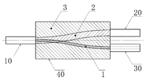
- FIG. 1 shows an example of an optical branching coupler according to the present invention.
- This optical branching coupler A is different from the first optical waveguide 1 extended from one end side (right end side according to FIG. 1) to the other end side (left end side according to FIG. 1) from the same one end side.
- a second optical waveguide 2 extending to the other end side of the path and joining the other end side to the other end side of the first optical waveguide 1, and the first optical waveguide 1 and the second optical waveguide
- the optical waveguide 2 is used as a core, and a cladding layer 3 covering the periphery of the core is provided.
- two-dot chain lines are the first port 10, the second port 20, and the third port 30 used when manufacturing the optical branching coupler A.
- 1st optical waveguide 1 and 2nd optical waveguide 2 are hardened
- the 2nd optical waveguide 2 can be comprised with the hardened
- the clad layer 3 can be comprised with the hardened
- the grad layer 3 can be made of a material having a lower refractive index than the second photo-curing resin such as a thermosetting resin.
- the second optical waveguide 2 does not necessarily need to be a cured product of the second photocured resin different from the first photocured resin, and may be a photocured product.
- the optical waveguide can be self-made by inputting light. it can.
- the waveguide can be self-aligned and connected to a plurality of optical axes that are not on the same straight line.
- the optical branching coupler can be configured without using optical components such as a filter and a lens.
- the first and second photo-curing resins may be photo-curing resins that are cured by light having a wavelength of 400 nm to 500 nm, for example, and may be used in a general self-forming waveguide technique.
- the clad layer 3 may be made of a material having a refractive index lower than that of the second photocurable resin, such as a photocurable resin that is cured by irradiation with ultraviolet rays.
- the first photocurable resin, the second photocurable resin, and the third photocurable resin are appropriately selected from, for example, the photocurable resins described in Patent Documents 1 and 2, and other known photocurable resins. Is possible.
- the refractive index n 2 of the second optical waveguide 2 is smaller than the refractive index n 1 of the first optical waveguide 1, and further, the cladding layer 3 refractive index n 3 of is smaller than the refractive indexes n 1, n 2 of the first optical waveguide 1 and the second waveguide 2.
- the second optical waveguide 2 acts to confine light in the first optical waveguide 1. Therefore, for example, when light is transmitted from the third port 30 through the first optical waveguide 1 to the first port 10, there is little light leakage to the second optical waveguide 2, and low loss and high quality. Optical transmission becomes possible.
- the ratio of the refractive indexes is represented by the following mathematical formula.
- n 1 : n 2 : n 3 about 1.54: about 1.52: about 1.45
- NA Numerical Aperture
- NA 12 , NA 13 , NA 23 can be calculated by the following formula.
- NA 12 (n 1 2 ⁇ n 2 2 ) 1/2
- NA 13 (n 1 2 -n 3 2 ) 1/2
- NA 23 (n 2 2 -n 3 2 ) 1/2
- the outer diameter of the first optical waveguide 1 is set smaller than the outer diameter of the second optical waveguide 2. As described above, when the outer diameter of the optical waveguide is set, for example, when light is transmitted by the thick second optical waveguide 2 from the first port 10 side toward the second port 20 side, the light is transmitted. Loss due to, for example, passing through the narrower first optical waveguide 1 can be reduced.
- the first optical waveguide 1 and the second optical waveguide 2 have a joint portion x on the other end side (the left end side in the drawing) and a substantially Y shape or a substantially V shape in which the opposite side is branched. Configured.
- the first optical waveguide 1 is contained in the second optical waveguide 2.
- the joint portion x is configured in a double core shape in which the second optical waveguide 2 covers the entire circumference of the first optical waveguide 1.
- the first port 10 is indicated by a solid line, but the optical branching coupler A according to the present invention may be configured such that the first port 10 is connected to the end portion of the junction part x The first port 10 may be omitted.
- the clad layer 3 has the first optical waveguide 1 and the second optical waveguide 2 as cores and covers the periphery of the core over the entire length in the longitudinal direction.
- the clad layer 3 can be formed in, for example, a cylindrical shape, a prismatic shape, or other three-dimensional shapes according to the inner surface shape of the container 40 described later.
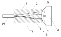
- the first port 10 the second port 20 separated from the first port 10 in the optical axis direction of the first port 10 (rightward in the illustrated example), and the second port 20 Covers the third port 30 that is arranged substantially parallel to the optical axis crossing direction (downward in the illustrated example) and the space between the second port 20 and the third port 30 and the first port 10.
- a container 40 that covers the space-side tip of each port is used.
- the first port 10, the second port 20, and the third port 30 are optical fibers having different core diameters.
- the core diameter of the first port 10 is c1
- the core diameter of the second port 20 is c2
- the core diameter of the third port 30 is c3
- the following relational expression is preferably satisfied.
- the container 40 is formed in a hollow three-dimensional shape that forms the outer surface shape of the cladding layer 3.
- the container 40 may be made of, for example, a hard material such as metal, hard synthetic resin, ceramic, or glass, and a window, an opening, or the like that transmits ultraviolet light is provided as necessary.
- a through-hole (not shown) that passes through the end portions of the second port 20 and the third port 30 is formed.
- a penetrating hole (not shown) that passes through the end portion of the first port 10 is provided on the other end side of the container 40.
- the wall of the container 40 is provided with an opening (not shown) for filling the first to third photo-curing resins and removing the uncured photo-curing resin.
- the optical branching coupler shown in FIG. 3 is manufactured by the self-forming waveguide technology using three fiber outgoing lights, and the low-loss coupler can be configured. It has become possible.
- the optical branching coupler A of the said structure comprises the optical transmission / reception module B shown in FIG. 4, for example.
- the transmission / reception module B in the illustrated example enters light into the optical branching coupler A to which the first port 10 is connected and the end face on the one end side (right end side in the illustrated example) of the first optical waveguide 1.
- the optical transceiver includes a light source unit 4 connected to the light source unit, a light receiving unit 5 connected to receive light from the end face on the one end side of the second optical waveguide 2, and a control circuit unit 6.
- the light source unit 4 is a light source device including a light emitting diode, a laser diode, and the like.
- the light receiving unit 5 is a light receiving device including a photodiode, a phototransistor, and the like.
- the light source unit 4 and the light receiving unit 5 are integrally supported by the control board 6.
- the control board 6 converts an electrical signal input from the outside into an optical signal and emits it from the light source unit 4 to the first optical waveguide 1, or an optical signal received from the second optical waveguide 2.
- This is an electronic circuit board having a circuit or the like for converting to an external output.
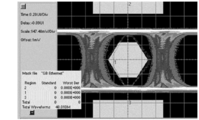
- a transceiver module B is connected to each of both ends of a 15 meter long SI-type 200/230 ⁇ m multimode fiber.
- the eye pattern was analyzed using a bit error rate tester (manufactured by Agilent Technologies (currently Keysight Technology) N4903A).
- FIG. 5 shows an eye pattern image when the transmission / reception module B having the optical branching coupler A is used.
- This eye pattern image has a plurality of overlapping waveforms at the same position (timing / voltage), indicating that the optical transmission quality is good.
- the inventors of the present application have made the refractive index of the second optical waveguide 2 smaller than the refractive index of the first optical waveguide 1, and the first optical waveguide 1 is changed to the second optical waveguide. It has been found that the optical transmission quality can be prevented from lowering due to the influence between the first optical waveguide 1 and the second optical waveguide 2 by making it thinner than 2, and the present invention has been completed.
- the angle between the first optical waveguide 1 and the second optical waveguide 2 can be reduced to, for example, about 0 to 10 °.
- the high optical transmission quality described above can be obtained. Therefore, the overall optical branching coupler A can be made thinner by reducing the dimension in the optical crossing direction.
- the optical branching coupler A is particularly suitable for constituting a pair of bidirectional communication devices, and can perform a gigabit class high-speed communication without a filter.
- the clad layer 3 made of a photo-curing resin is provided.
- the photo-curing resin clad layer 3 is omitted, and the surrounding gas or liquid (for example, It is also possible to use a cladding layer such as air or water.
- the outer diameter c2 of the second optical waveguide 2 is set to be substantially the same as the core diameter c1 in the first port 10, but as another example, the outer diameter c2 Can be made smaller than the core diameter c1.
- the first port 10 is an optical fiber having a single core and a single clad.
- the first port 10 is a core closer to the center. And a first clad covering the periphery of the core and a second cladding covering the periphery of the first cladding.
- the core diameter of the first port 10 is not less than the outer diameter of the first optical waveguide 1, and the first optical waveguide 1 is joined to the core of the first port 10.
- the outer diameter of the first cladding of the first port 10 is set to be equal to or larger than the outer diameter of the second optical waveguide 2 so that the second optical waveguide 2 covers the first optical waveguide 1 on the other end side. Then, the first port 10 is joined to the first cladding portion.
- the present invention is not limited to the above-described embodiment, and can be appropriately changed without departing from the gist of the present invention.
- First optical waveguide 2 Second optical waveguide 3: Cladding layer 4: Light source unit 5: Light receiving unit 10: First port 20: Second port 30: Third port 40: Container A: Optical branching coupler B: Transmission / reception module x: Joint part
Landscapes
- Physics & Mathematics (AREA)
- General Physics & Mathematics (AREA)
- Optics & Photonics (AREA)
- Engineering & Computer Science (AREA)
- Microelectronics & Electronic Packaging (AREA)
- Optical Integrated Circuits (AREA)
- Optical Couplings Of Light Guides (AREA)
Abstract
L'invention concerne un instrument de ramification/couplage optique dans lequel la qualité de transmission optique est accrue en empêchant une réduction de la qualité de transmission optique, ladite réduction étant provoquée, par exemple, par une âme de guide d'onde optique affectant une lumière d'une autre âme de guide d'onde optique au voisinage d'une section de jonction des deux âmes de guide d'onde optique. L'instrument de ramification/couplage optique comprend : un premier guide d'onde optique (1) qui est disposé en s'étendant entre un côté d'extrémité et un autre côté d'extrémité ; un second guide d'onde optique (2) qui est disposé en s'étendant sur un chemin distinct entre le même côté d'extrémité et l'autre côté d'extrémité, l'autre côté d'extrémité dudit second guide d'onde optique (2) étant joint à l'autre côté d'extrémité du premier guide d'ondes optique (1) ; et une couche de gaine (3) qui recouvre la périphérie du premier guide d'onde optique (1) et du second guide d'onde optique (2), les premier et second guides d'ondes optiques comprenant un produit durci d'une résine photodurcissante.
Priority Applications (2)
| Application Number | Priority Date | Filing Date | Title |
|---|---|---|---|
| DE112017001232.5T DE112017001232T5 (de) | 2016-03-09 | 2017-03-08 | Optische Verzweigungs-/Kopplungsvorrichtung und optisches Übertragungs-/Empfangsmodul |
| US16/081,277 US10473856B2 (en) | 2016-03-09 | 2017-03-08 | Optical branching/coupling device and optical transmission/reception module |
Applications Claiming Priority (2)
| Application Number | Priority Date | Filing Date | Title |
|---|---|---|---|
| JP2016-045209 | 2016-03-09 | ||
| JP2016045209A JP6643151B2 (ja) | 2016-03-09 | 2016-03-09 | 光分岐結合器及び光送受信モジュール |
Publications (1)
| Publication Number | Publication Date |
|---|---|
| WO2017155007A1 true WO2017155007A1 (fr) | 2017-09-14 |
Family
ID=59789531
Family Applications (1)
| Application Number | Title | Priority Date | Filing Date |
|---|---|---|---|
| PCT/JP2017/009345 Ceased WO2017155007A1 (fr) | 2016-03-09 | 2017-03-08 | Instrument de ramification/couplage optique et module d'émission/réception optique |
Country Status (4)
| Country | Link |
|---|---|
| US (1) | US10473856B2 (fr) |
| JP (1) | JP6643151B2 (fr) |
| DE (1) | DE112017001232T5 (fr) |
| WO (1) | WO2017155007A1 (fr) |
Families Citing this family (2)
| Publication number | Priority date | Publication date | Assignee | Title |
|---|---|---|---|---|
| JP7025740B2 (ja) * | 2017-04-27 | 2022-02-25 | アダマンド並木精密宝石株式会社 | 光分岐結合器及び光送受信モジュール |
| WO2021199377A1 (fr) * | 2020-04-01 | 2021-10-07 | 日本電信電話株式会社 | Élément de connexion optique, élément optique et procédé de fabrication d'élément optique |
Citations (3)
| Publication number | Priority date | Publication date | Assignee | Title |
|---|---|---|---|---|
| WO2007029717A1 (fr) * | 2005-09-06 | 2007-03-15 | Kabusiki Kaisha Toyota Chuo Kenkyusho | Guide d'onde optique et procédé de fabrication idoine |
| JP2010032584A (ja) * | 2008-07-25 | 2010-02-12 | Toyota Central R&D Labs Inc | 光導波路及び光モジュール、並びにそれらの製造方法 |
| JP2013045028A (ja) * | 2011-08-26 | 2013-03-04 | Tokai Univ | 分岐光導波路の製造方法及び光デバイス |
Family Cites Families (6)
| Publication number | Priority date | Publication date | Assignee | Title |
|---|---|---|---|---|
| GB9225274D0 (en) * | 1992-12-03 | 1993-01-27 | Int Computers Ltd | Electronic circuit assemblies |
| WO2005109084A1 (fr) * | 2004-05-12 | 2005-11-17 | Ls Cable Ltd. | Structure de guide d'onde optique de forme y assymetrique, et emetteur-recepteur pour la transmission d'un signal optique bidirectionnel utilisant cette structure |
| US7400801B1 (en) * | 2007-06-19 | 2008-07-15 | Owlink Technology, Inc. | Bidirectional HDCP module using single optical fiber and waveguide combiner/splitter |
| US20090028553A1 (en) * | 2007-07-27 | 2009-01-29 | Moshe Oron | Method and apparatus of detecting abnormal behavior in a passive optical network (PON) |
| JP4970364B2 (ja) | 2008-06-27 | 2012-07-04 | 豊田合成株式会社 | 光分岐結合器及びその製造方法 |
| JP4979649B2 (ja) | 2008-07-25 | 2012-07-18 | 株式会社豊田中央研究所 | 光モジュールの製造方法 |
-
2016
- 2016-03-09 JP JP2016045209A patent/JP6643151B2/ja active Active
-
2017
- 2017-03-08 DE DE112017001232.5T patent/DE112017001232T5/de active Pending
- 2017-03-08 WO PCT/JP2017/009345 patent/WO2017155007A1/fr not_active Ceased
- 2017-03-08 US US16/081,277 patent/US10473856B2/en active Active
Patent Citations (3)
| Publication number | Priority date | Publication date | Assignee | Title |
|---|---|---|---|---|
| WO2007029717A1 (fr) * | 2005-09-06 | 2007-03-15 | Kabusiki Kaisha Toyota Chuo Kenkyusho | Guide d'onde optique et procédé de fabrication idoine |
| JP2010032584A (ja) * | 2008-07-25 | 2010-02-12 | Toyota Central R&D Labs Inc | 光導波路及び光モジュール、並びにそれらの製造方法 |
| JP2013045028A (ja) * | 2011-08-26 | 2013-03-04 | Tokai Univ | 分岐光導波路の製造方法及び光デバイス |
Also Published As
| Publication number | Publication date |
|---|---|
| US10473856B2 (en) | 2019-11-12 |
| JP6643151B2 (ja) | 2020-02-12 |
| US20190079244A1 (en) | 2019-03-14 |
| DE112017001232T5 (de) | 2018-12-13 |
| JP2017161687A (ja) | 2017-09-14 |
Similar Documents
| Publication | Publication Date | Title |
|---|---|---|
| JP6644080B2 (ja) | 光コネクタ及び光コネクタシステム並びにこれらを備えたアクティブ光ケーブル | |
| JP2020501198A (ja) | マルチチャネル光結合器アレイ | |
| JP2019152804A (ja) | 光コネクタ | |
| CN116250191B (zh) | 多芯光纤和光传输系统 | |
| JP2023529528A (ja) | 光結合および光学場のモード選択分離または重ね合わせ | |
| JP2017134290A (ja) | 光デバイス | |
| WO2018042984A1 (fr) | Structure de connexion optique | |
| WO2017155007A1 (fr) | Instrument de ramification/couplage optique et module d'émission/réception optique | |
| JP4636439B2 (ja) | 方向性光結合器の2つの直線光導波路のコア幅及びコア間の距離の計算方法 | |
| JP4351130B2 (ja) | 光接続装置の製造法及びその光接続装置 | |
| CN104765105B (zh) | 机械传输mt插芯及单模光纤连接器 | |
| KR100585016B1 (ko) | 고차 모드 제거 필터링 기능을 갖는 단일모드 광섬유 구조 | |
| JP2016151651A (ja) | 光ファイバ及び光伝送システム | |
| JP2017187680A (ja) | 光デバイス | |
| JP7025740B2 (ja) | 光分岐結合器及び光送受信モジュール | |
| JP2017161688A (ja) | 光分岐結合器及び該光分岐結合器の製造方法並びに光送受信モジュール | |
| CN201757795U (zh) | 光发射次组装模块 | |
| JP4390270B2 (ja) | 光ファイバの接続方法及び光フィルタの製造方法 | |
| US6874947B2 (en) | Optical component | |
| KR100963206B1 (ko) | 광섬유 커넥터 | |
| JP2010032273A (ja) | 活線検出装置 | |
| JP4524390B2 (ja) | 光接続装置の製造方法 | |
| US20250189717A1 (en) | Multicore optical fiber, optical combiner, and method of measuring fiber characteristics | |
| JP2007171769A (ja) | 光合波導波路 | |
| KR100493098B1 (ko) | 평면 도파로 구조의 광 모듈 |
Legal Events
| Date | Code | Title | Description |
|---|---|---|---|
| 121 | Ep: the epo has been informed by wipo that ep was designated in this application |
Ref document number: 17763347 Country of ref document: EP Kind code of ref document: A1 |
|
| 122 | Ep: pct application non-entry in european phase |
Ref document number: 17763347 Country of ref document: EP Kind code of ref document: A1 |