WO2017155007A1 - 光分岐結合器及び光送受信モジュール - Google Patents
光分岐結合器及び光送受信モジュール Download PDFInfo
- Publication number
- WO2017155007A1 WO2017155007A1 PCT/JP2017/009345 JP2017009345W WO2017155007A1 WO 2017155007 A1 WO2017155007 A1 WO 2017155007A1 JP 2017009345 W JP2017009345 W JP 2017009345W WO 2017155007 A1 WO2017155007 A1 WO 2017155007A1
- Authority
- WO
- WIPO (PCT)
- Prior art keywords
- optical waveguide
- optical
- end side
- waveguide
- port
- Prior art date
- Legal status (The legal status is an assumption and is not a legal conclusion. Google has not performed a legal analysis and makes no representation as to the accuracy of the status listed.)
- Ceased
Links
Images


Classifications
-
- G—PHYSICS
- G02—OPTICS
- G02B—OPTICAL ELEMENTS, SYSTEMS OR APPARATUS
- G02B6/00—Light guides; Structural details of arrangements comprising light guides and other optical elements, e.g. couplings
- G02B6/10—Light guides; Structural details of arrangements comprising light guides and other optical elements, e.g. couplings of the optical waveguide type
- G02B6/12—Light guides; Structural details of arrangements comprising light guides and other optical elements, e.g. couplings of the optical waveguide type of the integrated circuit kind
- G02B6/13—Integrated optical circuits characterised by the manufacturing method
- G02B6/138—Integrated optical circuits characterised by the manufacturing method by using polymerisation
-
- G—PHYSICS
- G02—OPTICS
- G02B—OPTICAL ELEMENTS, SYSTEMS OR APPARATUS
- G02B6/00—Light guides; Structural details of arrangements comprising light guides and other optical elements, e.g. couplings
- G02B6/10—Light guides; Structural details of arrangements comprising light guides and other optical elements, e.g. couplings of the optical waveguide type
- G02B6/12—Light guides; Structural details of arrangements comprising light guides and other optical elements, e.g. couplings of the optical waveguide type of the integrated circuit kind
- G02B6/122—Basic optical elements, e.g. light-guiding paths
- G02B6/125—Bends, branchings or intersections
-
- G—PHYSICS
- G02—OPTICS
- G02B—OPTICAL ELEMENTS, SYSTEMS OR APPARATUS
- G02B6/00—Light guides; Structural details of arrangements comprising light guides and other optical elements, e.g. couplings
- G02B6/02—Optical fibres with cladding with or without a coating
- G02B6/036—Optical fibres with cladding with or without a coating core or cladding comprising multiple layers
- G02B6/03616—Optical fibres characterised both by the number of different refractive index layers around the central core segment, i.e. around the innermost high index core layer, and their relative refractive index difference
-
- G—PHYSICS
- G02—OPTICS
- G02B—OPTICAL ELEMENTS, SYSTEMS OR APPARATUS
- G02B6/00—Light guides; Structural details of arrangements comprising light guides and other optical elements, e.g. couplings
- G02B6/10—Light guides; Structural details of arrangements comprising light guides and other optical elements, e.g. couplings of the optical waveguide type
- G02B6/12—Light guides; Structural details of arrangements comprising light guides and other optical elements, e.g. couplings of the optical waveguide type of the integrated circuit kind
- G02B6/122—Basic optical elements, e.g. light-guiding paths
- G02B6/1221—Basic optical elements, e.g. light-guiding paths made from organic materials
-
- G—PHYSICS
- G02—OPTICS
- G02B—OPTICAL ELEMENTS, SYSTEMS OR APPARATUS
- G02B6/00—Light guides; Structural details of arrangements comprising light guides and other optical elements, e.g. couplings
- G02B6/10—Light guides; Structural details of arrangements comprising light guides and other optical elements, e.g. couplings of the optical waveguide type
- G02B6/12—Light guides; Structural details of arrangements comprising light guides and other optical elements, e.g. couplings of the optical waveguide type of the integrated circuit kind
- G02B6/13—Integrated optical circuits characterised by the manufacturing method
-
- G—PHYSICS
- G02—OPTICS
- G02B—OPTICAL ELEMENTS, SYSTEMS OR APPARATUS
- G02B6/00—Light guides; Structural details of arrangements comprising light guides and other optical elements, e.g. couplings
- G02B6/24—Coupling light guides
- G02B6/26—Optical coupling means
- G02B6/28—Optical coupling means having data bus means, i.e. plural waveguides interconnected and providing an inherently bidirectional system by mixing and splitting signals
-
- G—PHYSICS
- G02—OPTICS
- G02B—OPTICAL ELEMENTS, SYSTEMS OR APPARATUS
- G02B6/00—Light guides; Structural details of arrangements comprising light guides and other optical elements, e.g. couplings
- G02B6/24—Coupling light guides
- G02B6/26—Optical coupling means
- G02B6/30—Optical coupling means for use between fibre and thin-film device
-
- G—PHYSICS
- G02—OPTICS
- G02B—OPTICAL ELEMENTS, SYSTEMS OR APPARATUS
- G02B6/00—Light guides; Structural details of arrangements comprising light guides and other optical elements, e.g. couplings
- G02B6/24—Coupling light guides
- G02B6/42—Coupling light guides with opto-electronic elements
-
- G—PHYSICS
- G02—OPTICS
- G02B—OPTICAL ELEMENTS, SYSTEMS OR APPARATUS
- G02B6/00—Light guides; Structural details of arrangements comprising light guides and other optical elements, e.g. couplings
- G02B6/24—Coupling light guides
- G02B6/42—Coupling light guides with opto-electronic elements
- G02B6/4201—Packages, e.g. shape, construction, internal or external details
- G02B6/4204—Packages, e.g. shape, construction, internal or external details the coupling comprising intermediate optical elements, e.g. lenses, holograms
- G02B6/4214—Packages, e.g. shape, construction, internal or external details the coupling comprising intermediate optical elements, e.g. lenses, holograms the intermediate optical element having redirecting reflective means, e.g. mirrors, prisms for deflecting the radiation from horizontal to down- or upward direction toward a device
-
- G—PHYSICS
- G02—OPTICS
- G02B—OPTICAL ELEMENTS, SYSTEMS OR APPARATUS
- G02B6/00—Light guides; Structural details of arrangements comprising light guides and other optical elements, e.g. couplings
- G02B6/24—Coupling light guides
- G02B6/42—Coupling light guides with opto-electronic elements
- G02B6/43—Arrangements comprising a plurality of opto-electronic elements and associated optical interconnections
-
- G—PHYSICS
- G02—OPTICS
- G02B—OPTICAL ELEMENTS, SYSTEMS OR APPARATUS
- G02B6/00—Light guides; Structural details of arrangements comprising light guides and other optical elements, e.g. couplings
- G02B6/10—Light guides; Structural details of arrangements comprising light guides and other optical elements, e.g. couplings of the optical waveguide type
- G02B6/12—Light guides; Structural details of arrangements comprising light guides and other optical elements, e.g. couplings of the optical waveguide type of the integrated circuit kind
- G02B2006/12133—Functions
- G02B2006/1215—Splitter
Definitions
- the present invention relates to an optical branching coupler and an optical transmission / reception module that can be used as an optical branching unit or a coupler.
- Patent Document 1 for example, a hollow casing, three optical fibers connected to the wall surface of the casing, and the casing are supported in the casing
- an optical module that includes an optical filter (half mirror, WDM filter, etc.) and a cured product of a photo-curing resin filled in the casing.
- the light curable resin in the housing is cured by light irradiated from the optical fiber, and three cores are formed on both sides of the optical filter.
- Such a manufacturing technique is referred to as a self-forming waveguide technique.
- a clad made of a material having a refractive index smaller than those of the cores is formed so as to cover the three cores.
- the structure in the housing becomes complicated and the structure becomes relatively expensive.
- the two branched optical waveguide cores must be set at a specific angle, there is a possibility of increasing the size in the direction intersecting the optical axis.
- the optical transmission quality is caused by the fact that the light of one optical waveguide core is influenced by the other optical waveguide core in the vicinity of the joint of the two optical waveguide cores. There is a risk of lowering.
- the optical branching coupler of the present invention is provided with a first optical waveguide extending from one end side to the other end side, and extended from the same one end side to the other end side by another path. And a second optical waveguide having the other end joined to the other end of the first optical waveguide, and a cladding layer covering the periphery of the first optical waveguide and the second optical waveguide.
- the first and second optical waveguides are cured products of the same photocurable resin.
- the first optical waveguide extending from one end side to the other end side is extended by another path from the same one end side to the other end side, and the other end side
- the first optical waveguide Is a cured product of the first photo-curing resin
- the second optical waveguide is a cured product of the second photo-curing resin different from the first photo-curing resin
- the second optical waveguide is refracted.
- the refractive index is smaller than the refractive index of the first optical waveguide
- the refractive index of the cladding layer is smaller than the refractive index of the second optical waveguide.
- the optical branching coupler of the present invention can make an optical waveguide by inputting light during manufacturing.
- the waveguide can be self-aligned and connected to a plurality of optical axes that are not on the same straight line.
- the optical branching coupler can be configured without using optical components such as a filter and a lens.
- an optical branching coupler with improved optical transmission quality can be manufactured by a self-forming waveguide technique.
- the optical transmission quality can be further improved.
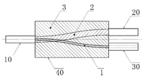
- FIG. 1 shows an example of an optical branching coupler according to the present invention.
- This optical branching coupler A is different from the first optical waveguide 1 extended from one end side (right end side according to FIG. 1) to the other end side (left end side according to FIG. 1) from the same one end side.
- a second optical waveguide 2 extending to the other end side of the path and joining the other end side to the other end side of the first optical waveguide 1, and the first optical waveguide 1 and the second optical waveguide
- the optical waveguide 2 is used as a core, and a cladding layer 3 covering the periphery of the core is provided.
- two-dot chain lines are the first port 10, the second port 20, and the third port 30 used when manufacturing the optical branching coupler A.
- 1st optical waveguide 1 and 2nd optical waveguide 2 are hardened
- the 2nd optical waveguide 2 can be comprised with the hardened
- the clad layer 3 can be comprised with the hardened
- the grad layer 3 can be made of a material having a lower refractive index than the second photo-curing resin such as a thermosetting resin.
- the second optical waveguide 2 does not necessarily need to be a cured product of the second photocured resin different from the first photocured resin, and may be a photocured product.
- the optical waveguide can be self-made by inputting light. it can.
- the waveguide can be self-aligned and connected to a plurality of optical axes that are not on the same straight line.
- the optical branching coupler can be configured without using optical components such as a filter and a lens.
- the first and second photo-curing resins may be photo-curing resins that are cured by light having a wavelength of 400 nm to 500 nm, for example, and may be used in a general self-forming waveguide technique.
- the clad layer 3 may be made of a material having a refractive index lower than that of the second photocurable resin, such as a photocurable resin that is cured by irradiation with ultraviolet rays.
- the first photocurable resin, the second photocurable resin, and the third photocurable resin are appropriately selected from, for example, the photocurable resins described in Patent Documents 1 and 2, and other known photocurable resins. Is possible.
- the refractive index n 2 of the second optical waveguide 2 is smaller than the refractive index n 1 of the first optical waveguide 1, and further, the cladding layer 3 refractive index n 3 of is smaller than the refractive indexes n 1, n 2 of the first optical waveguide 1 and the second waveguide 2.
- the second optical waveguide 2 acts to confine light in the first optical waveguide 1. Therefore, for example, when light is transmitted from the third port 30 through the first optical waveguide 1 to the first port 10, there is little light leakage to the second optical waveguide 2, and low loss and high quality. Optical transmission becomes possible.
- the ratio of the refractive indexes is represented by the following mathematical formula.
- n 1 : n 2 : n 3 about 1.54: about 1.52: about 1.45
- NA Numerical Aperture
- NA 12 , NA 13 , NA 23 can be calculated by the following formula.
- NA 12 (n 1 2 ⁇ n 2 2 ) 1/2
- NA 13 (n 1 2 -n 3 2 ) 1/2
- NA 23 (n 2 2 -n 3 2 ) 1/2
- the outer diameter of the first optical waveguide 1 is set smaller than the outer diameter of the second optical waveguide 2. As described above, when the outer diameter of the optical waveguide is set, for example, when light is transmitted by the thick second optical waveguide 2 from the first port 10 side toward the second port 20 side, the light is transmitted. Loss due to, for example, passing through the narrower first optical waveguide 1 can be reduced.
- the first optical waveguide 1 and the second optical waveguide 2 have a joint portion x on the other end side (the left end side in the drawing) and a substantially Y shape or a substantially V shape in which the opposite side is branched. Configured.
- the first optical waveguide 1 is contained in the second optical waveguide 2.
- the joint portion x is configured in a double core shape in which the second optical waveguide 2 covers the entire circumference of the first optical waveguide 1.
- the first port 10 is indicated by a solid line, but the optical branching coupler A according to the present invention may be configured such that the first port 10 is connected to the end portion of the junction part x The first port 10 may be omitted.
- the clad layer 3 has the first optical waveguide 1 and the second optical waveguide 2 as cores and covers the periphery of the core over the entire length in the longitudinal direction.
- the clad layer 3 can be formed in, for example, a cylindrical shape, a prismatic shape, or other three-dimensional shapes according to the inner surface shape of the container 40 described later.
- the first port 10 the second port 20 separated from the first port 10 in the optical axis direction of the first port 10 (rightward in the illustrated example), and the second port 20 Covers the third port 30 that is arranged substantially parallel to the optical axis crossing direction (downward in the illustrated example) and the space between the second port 20 and the third port 30 and the first port 10.
- a container 40 that covers the space-side tip of each port is used.
- the first port 10, the second port 20, and the third port 30 are optical fibers having different core diameters.
- the core diameter of the first port 10 is c1
- the core diameter of the second port 20 is c2
- the core diameter of the third port 30 is c3
- the following relational expression is preferably satisfied.
- the container 40 is formed in a hollow three-dimensional shape that forms the outer surface shape of the cladding layer 3.
- the container 40 may be made of, for example, a hard material such as metal, hard synthetic resin, ceramic, or glass, and a window, an opening, or the like that transmits ultraviolet light is provided as necessary.
- a through-hole (not shown) that passes through the end portions of the second port 20 and the third port 30 is formed.
- a penetrating hole (not shown) that passes through the end portion of the first port 10 is provided on the other end side of the container 40.
- the wall of the container 40 is provided with an opening (not shown) for filling the first to third photo-curing resins and removing the uncured photo-curing resin.
- the optical branching coupler shown in FIG. 3 is manufactured by the self-forming waveguide technology using three fiber outgoing lights, and the low-loss coupler can be configured. It has become possible.
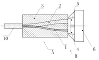
- the optical branching coupler A of the said structure comprises the optical transmission / reception module B shown in FIG. 4, for example.
- the transmission / reception module B in the illustrated example enters light into the optical branching coupler A to which the first port 10 is connected and the end face on the one end side (right end side in the illustrated example) of the first optical waveguide 1.
- the optical transceiver includes a light source unit 4 connected to the light source unit, a light receiving unit 5 connected to receive light from the end face on the one end side of the second optical waveguide 2, and a control circuit unit 6.
- the light source unit 4 is a light source device including a light emitting diode, a laser diode, and the like.
- the light receiving unit 5 is a light receiving device including a photodiode, a phototransistor, and the like.
- the light source unit 4 and the light receiving unit 5 are integrally supported by the control board 6.
- the control board 6 converts an electrical signal input from the outside into an optical signal and emits it from the light source unit 4 to the first optical waveguide 1, or an optical signal received from the second optical waveguide 2.
- This is an electronic circuit board having a circuit or the like for converting to an external output.
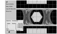
- a transceiver module B is connected to each of both ends of a 15 meter long SI-type 200/230 ⁇ m multimode fiber.
- the eye pattern was analyzed using a bit error rate tester (manufactured by Agilent Technologies (currently Keysight Technology) N4903A).
- FIG. 5 shows an eye pattern image when the transmission / reception module B having the optical branching coupler A is used.
- This eye pattern image has a plurality of overlapping waveforms at the same position (timing / voltage), indicating that the optical transmission quality is good.
- the inventors of the present application have made the refractive index of the second optical waveguide 2 smaller than the refractive index of the first optical waveguide 1, and the first optical waveguide 1 is changed to the second optical waveguide. It has been found that the optical transmission quality can be prevented from lowering due to the influence between the first optical waveguide 1 and the second optical waveguide 2 by making it thinner than 2, and the present invention has been completed.
- the angle between the first optical waveguide 1 and the second optical waveguide 2 can be reduced to, for example, about 0 to 10 °.
- the high optical transmission quality described above can be obtained. Therefore, the overall optical branching coupler A can be made thinner by reducing the dimension in the optical crossing direction.
- the optical branching coupler A is particularly suitable for constituting a pair of bidirectional communication devices, and can perform a gigabit class high-speed communication without a filter.
- the clad layer 3 made of a photo-curing resin is provided.
- the photo-curing resin clad layer 3 is omitted, and the surrounding gas or liquid (for example, It is also possible to use a cladding layer such as air or water.
- the outer diameter c2 of the second optical waveguide 2 is set to be substantially the same as the core diameter c1 in the first port 10, but as another example, the outer diameter c2 Can be made smaller than the core diameter c1.
- the first port 10 is an optical fiber having a single core and a single clad.
- the first port 10 is a core closer to the center. And a first clad covering the periphery of the core and a second cladding covering the periphery of the first cladding.
- the core diameter of the first port 10 is not less than the outer diameter of the first optical waveguide 1, and the first optical waveguide 1 is joined to the core of the first port 10.
- the outer diameter of the first cladding of the first port 10 is set to be equal to or larger than the outer diameter of the second optical waveguide 2 so that the second optical waveguide 2 covers the first optical waveguide 1 on the other end side. Then, the first port 10 is joined to the first cladding portion.
- the present invention is not limited to the above-described embodiment, and can be appropriately changed without departing from the gist of the present invention.
- First optical waveguide 2 Second optical waveguide 3: Cladding layer 4: Light source unit 5: Light receiving unit 10: First port 20: Second port 30: Third port 40: Container A: Optical branching coupler B: Transmission / reception module x: Joint part
Landscapes
- Physics & Mathematics (AREA)
- General Physics & Mathematics (AREA)
- Optics & Photonics (AREA)
- Engineering & Computer Science (AREA)
- Microelectronics & Electronic Packaging (AREA)
- Optical Integrated Circuits (AREA)
- Optical Couplings Of Light Guides (AREA)
Abstract
二本の光導波路コアの接合部付近で、一方の光導波路コアの光が、他方の光導波路コアに影響されること等に起因した、光伝送品質の低下を防ぎ、光伝送品質が向上した光分岐結合器を提供する。本発明の光分岐結合器は、一端側から他端側へ延設された第1の光導波路1と、同じ一端側から他端側へ別経路にて延設されるとともに該他端側を第1の光導波路1の前記他端側に接合した第2の光導波路2と、これら第1の光導波路1及び第2の光導波路2の周囲を覆うクラッド層3とを備え、第1及び第2の光導波路が光硬化樹脂の硬化物よりなる。
Description
本発明は、光の分岐器や結合器等として使用可能な光分岐結合器及び光送受信モジュールに関するものである。
従来、この種の発明には、例えば特許文献1に記載されるもののように、中空状の筐体と、該筐体の壁面に接続された三つの光ファイバと、前記筐体内に支持された光学フィルタ(ハーフミラーやWDMフィルタ等)と、前記筐体内に充填された光硬化樹脂の硬化物とを具備した光モジュールがある。
この光モジュールの製造方法では、前記光ファイバから照射される光により筐体内の光硬化樹脂を硬化させて、前記光フィルタの両側に三つコアを形成する。このような製造技術は、自己形成導波路技術と呼称される。この後、前記三つのコアを被覆するように、これらコアよりも屈折率が小さい材料からなるクラッドを形成する。
また、他の従来技術としては、例えば特許文献2に記載されるもののように、自己形成導波路技術により、フィルターレスの分岐構造を形成したものもある。この従来技術では、分岐された二本の光導波路コアの角度が、10度以上の30度以下に限定されており、これによって、設計及び製造時の光軸合せの困難が解消され、光損失の増加を抑制できるとしている。
しかしながら、前者従来技術では、ハーフミラーやWDMフィルタ等の光学フィルタを内在しているため、筐体内の構造が複雑になる上、比較的高価な構成になってしまう。
後者従来技術では、分岐された二本の光導波路コアを特定の角度としなければならないため、光軸交差方向に大型化してしまう可能性がある。
また、前記何れの従来技術においても、二本の光導波路コアの接合部付近で、一方の光導波路コアの光が、他方の光導波路コアに影響されること等に起因して、光伝送品質の低下をまねくおそれがある。
後者従来技術では、分岐された二本の光導波路コアを特定の角度としなければならないため、光軸交差方向に大型化してしまう可能性がある。
また、前記何れの従来技術においても、二本の光導波路コアの接合部付近で、一方の光導波路コアの光が、他方の光導波路コアに影響されること等に起因して、光伝送品質の低下をまねくおそれがある。
このような課題に鑑みて、本発明の光分岐結合器は、一端側から他端側へ延設された第1の光導波路と、同じ一端側から他端側へ別経路にて延設されるとともに、該他端側を前記第1の光導波路の前記他端側に接合した第2の光導波路と、これら第1の光導波路及び第2の光導波路の周囲を覆うクラッド層とを備え、第1及び第2の光導波路が同じ光硬化樹脂の硬化物であることを特徴とする。
また、本発明第2の態様では、一端側から他端側へ延設された第1の光導波路と、同じ一端側から他端側へ別経路にて延設されるとともに、該他端側を前記第1の光導波路の前記他端側に接合した第2の光導波路と、これら第1の光導波路及び第2の光導波路の周囲を覆うクラッド層とを備え、前記第1の光導波路が第1の光硬化樹脂の硬化物であり、前記第2の光導波路が前記第1の光硬化樹脂とは異なる第2の光硬化樹脂の硬化物であり、前記第2の光導波路の屈折率が、前記第1の光導波路の屈折率よりも小さく、前記クラッド層の屈折率が、前記第2の光導波路の屈折率よりも小さいことを特徴とする。
上述した基本構造を用いたことで本発明の光分岐結合器は、製造に際して、光を入力させることにより、光導波路を自己的につくることができる。また、同一直線状に無い複数の光軸に対して、導波路を自己調芯接続することが可能となる。加えて、光分岐結合器を、フィルタ及びレンズ等の光学部品を用いずに構成することができる。
即ち、この様な構造を具備することによって、本発明では、光伝送品質を向上した光分岐結合器を自己形成導波路技術によって製造することが可能となっている。
また、前記第2の態様の光分岐結合器では、光伝送品質を更に向上することができる。
以下、図面を参照しながら本発明の実施形態を説明する。以下、異なる図における同一符号は同一部位を示しており、重複する説明は適宜省略する。
図1は、本発明に係る光分岐結合器の一例を示す。
この光分岐結合器Aは、一端側(図1によれば右端側)から他端側(図1によれば左端側)へ延設された第1の光導波路1と、同じ一端側から別経路にて他端側へ延設されるとともに該他端側を第1の光導波路1の前記他端側に接合した第2の光導波路2と、これら第1の光導波路1及び第2の光導波路2をコアとして該コアの周囲を覆うクラッド層3とを具備している。
なお、図1中、二点鎖線は、光分岐結合器Aを製造する際に用いられた第1ポート10、第2ポート20及び第3ポート30である。
この光分岐結合器Aは、一端側(図1によれば右端側)から他端側(図1によれば左端側)へ延設された第1の光導波路1と、同じ一端側から別経路にて他端側へ延設されるとともに該他端側を第1の光導波路1の前記他端側に接合した第2の光導波路2と、これら第1の光導波路1及び第2の光導波路2をコアとして該コアの周囲を覆うクラッド層3とを具備している。
なお、図1中、二点鎖線は、光分岐結合器Aを製造する際に用いられた第1ポート10、第2ポート20及び第3ポート30である。
第1の光導波路1及び第2の光導波路2は光硬化樹脂の硬化物である。第2の光導波路2は、第1の光硬化樹脂とは異なる第2の光硬化樹脂の硬化物で構成することができる。そして、クラッド層3は、第1の光硬化樹脂及び第2の光硬化樹脂とは異なる第3の光硬化樹脂の硬化物で構成することができる。尚、グラッド層3は、熱硬化性樹脂といった第2の光硬化樹脂よりも屈折率の低い材質を用いることが可能である。
尚、前記第2の光導波路2は、必ずしも第1の光硬化樹脂とは異なる第2の光硬化樹脂の硬化物である必要はなく、光硬化物であれば良い。第1の光導波路1、第2の光導波路2が光硬化樹脂の硬化物よりなる本発明の光分岐結合器を製造するに際して、光を入力させることにより、光導波路を自己的につくることができる。また、同一直線状に無い複数の光軸に対して、導波路を自己調芯接続することが可能となる。加えて、光分岐結合器を、フィルタ及びレンズ等の光学部品を用いずに構成することができる。
第1及び第2の光硬化樹脂は、例えば400nm~500nmの波長の光により硬化する光硬化樹脂であればよく、一般的な自己形成導波路技術に用いられるものとすればよい。
クラッド層3は、紫外線の照射により硬化する光硬化樹脂等、第2の光硬化性樹脂よりも屈折率の低い材質であればよい。
これら第1の光硬化樹脂、第2の光硬化樹脂及び第3の光硬化樹脂は、例えば、特許文献1及び2に記載された光硬化樹脂や、その他の周知の光硬化樹脂から適宜に選択することが可能である。
そして、前記光硬化樹脂に異なるものを用いることにより、第2の光導波路2の屈折率n2が、第1の光導波路1の屈折率n1よりも小さくなっており、さらに、クラッド層3の屈折率n3が、第1の光導波路1及び第2の光導波路2の屈折率n1,n2よりも小さくなっている。
クラッド層3は、紫外線の照射により硬化する光硬化樹脂等、第2の光硬化性樹脂よりも屈折率の低い材質であればよい。
これら第1の光硬化樹脂、第2の光硬化樹脂及び第3の光硬化樹脂は、例えば、特許文献1及び2に記載された光硬化樹脂や、その他の周知の光硬化樹脂から適宜に選択することが可能である。
そして、前記光硬化樹脂に異なるものを用いることにより、第2の光導波路2の屈折率n2が、第1の光導波路1の屈折率n1よりも小さくなっており、さらに、クラッド層3の屈折率n3が、第1の光導波路1及び第2の光導波路2の屈折率n1,n2よりも小さくなっている。
このような屈折率の設定によれば、第1の光導波路1においては、第2の光導波路2に対し、該第1の光導波路1内に光を閉じ込める作用が働く。このため、例えば、第3ポート30から第1の光導波路1を通り、第1ポート10へ光を伝送した場合に、第2の光導波路2への光の漏れが少なく、低損失且つ高品質な光伝送が可能になる。
本実施の形態の好ましい一例では、前記屈折率の比が以下の数式の関係になっている。
n1:n2:n3=約1.54:約1.52:約1.45
また、第1の光導波路1と第2の光導波路2間、第1の光導波路1とクラッド層3間、第2の光導波路2とクラッド層3間のNA(Numerical Aperture:開口数)を、NA12、NA13、NA23とし、以下の式により計算することができる。
NA12=(n1 2-n2 2)1/2
NA13=(n1 2-n3 2)1/2
NA23=(n2 2-n3 2)1/2
本実施の形態の好ましい一例では、以下の数式の関係が成り立つ。
NA13>NA23>NA12
n1:n2:n3=約1.54:約1.52:約1.45
また、第1の光導波路1と第2の光導波路2間、第1の光導波路1とクラッド層3間、第2の光導波路2とクラッド層3間のNA(Numerical Aperture:開口数)を、NA12、NA13、NA23とし、以下の式により計算することができる。
NA12=(n1 2-n2 2)1/2
NA13=(n1 2-n3 2)1/2
NA23=(n2 2-n3 2)1/2
本実施の形態の好ましい一例では、以下の数式の関係が成り立つ。
NA13>NA23>NA12
また、第1の光導波路1の外径は、第2の光導波路2の外径よりも小さく設定されている。
このように、光導波路の外径を設定すると、例えば、第1ポート10側から第2ポート20側へ向かうように、太い方の第2の光導波路2によって光を伝送した場合に、その光が細い方の第1の光導波路1へ抜けること等による損失を低減することができる。
このように、光導波路の外径を設定すると、例えば、第1ポート10側から第2ポート20側へ向かうように、太い方の第2の光導波路2によって光を伝送した場合に、その光が細い方の第1の光導波路1へ抜けること等による損失を低減することができる。
第1の光導波路1と第2の光導波路2は、前記他端側(図示の左端側)に接合部分xを有するとともに、その逆側を枝分かれ状に形成した略Y字状もしくは略V字状に構成される。
接合部分xでは、図2に示すように、第1の光導波路1が第2の光導波路2に内在される。換言すれば、接合部分xは、第1の光導波路1の全周を第2の光導波路2が覆ったダブルコア状に構成される。
接合部分xでは、図2に示すように、第1の光導波路1が第2の光導波路2に内在される。換言すれば、接合部分xは、第1の光導波路1の全周を第2の光導波路2が覆ったダブルコア状に構成される。
なお、図2では、第1ポート10を実線で示しているが、本発明に係る光分岐結合器Aは、接合部分xの端部に第1ポート10が接続された態様としてもよいし、第1ポート10の無い態様としてもよい。
クラッド層3は、第1の光導波路1及び第2の光導波路2をコアとし、このコアの周囲を長手方向の全長にわたって覆っている。
このクラッド層3は、後述する容器40の内面形状に応じて、例えば、円柱状や、角柱状、その他の立体形状に形成することが可能である。
このクラッド層3は、後述する容器40の内面形状に応じて、例えば、円柱状や、角柱状、その他の立体形状に形成することが可能である。
次に、上記構成の光分岐結合器Aについて、その製造方法を詳細に説明する。
この製造方法では、第1ポート10と、第1ポート10に対し該第1ポート10の光軸方向(図示例によれば右方向)に離れた第2ポート20と、第2ポート20に対し光軸交差方向(図示例によれば下方向)へ間隔を置いて略平行に並ぶ第3ポート30と、第2ポート20及び第3ポート30と第1ポート10との間の空間を覆うとともに各ポートの前記空間側の先端部を覆う容器40とが用いられる。
この製造方法では、第1ポート10と、第1ポート10に対し該第1ポート10の光軸方向(図示例によれば右方向)に離れた第2ポート20と、第2ポート20に対し光軸交差方向(図示例によれば下方向)へ間隔を置いて略平行に並ぶ第3ポート30と、第2ポート20及び第3ポート30と第1ポート10との間の空間を覆うとともに各ポートの前記空間側の先端部を覆う容器40とが用いられる。
第1ポート10、第2ポート20及び第3ポート30は、それぞれ、コア径が異なる光ファイバである。
第1ポート10のコア径をc1、第2ポート20のコア径をc2、第3ポート30のコア径をc3とすると、以下の関係式が成り立つことが好ましい。
c1≧c2≧c3
第1ポート10のコア径をc1、第2ポート20のコア径をc2、第3ポート30のコア径をc3とすると、以下の関係式が成り立つことが好ましい。
c1≧c2≧c3
特に、本実施の形態の好ましい態様では、前記コア径の関係を以下のようにしている。
c1=c2>c3
c1=c2>c3
また、容器40は、クラッド層3の外面形状を形作る中空立体状に形成される。この容器40の材質は、例えば、金属や硬質合成樹脂、セラミック、ガラス等の硬質材料とすればよく、必要に応じて、紫外線光を透過させる窓や開口等が設けられる。
この容器40の一端側には、第2ポート20及び第3ポート30の端部を挿通する貫通状の孔(図示せず)が形成される。
また、容器40の他端側には、第1ポート10の端部を挿通する貫通状の孔(図示せず)が設けられる。
また、この容器40の壁部には、第1~3の光硬化樹脂を充填したり、未硬化の光硬化樹脂を除去したりするための開口部(図示せず)が設けられている。
この容器40の一端側には、第2ポート20及び第3ポート30の端部を挿通する貫通状の孔(図示せず)が形成される。
また、容器40の他端側には、第1ポート10の端部を挿通する貫通状の孔(図示せず)が設けられる。
また、この容器40の壁部には、第1~3の光硬化樹脂を充填したり、未硬化の光硬化樹脂を除去したりするための開口部(図示せず)が設けられている。
ここで、本実施形態に於いて、図3に示す光分岐結合器は3本のファイバ出射光を用いた自己形成導波路技術により製造しており、低損失の当該結合器を構成することが可能となった。
そして、上記構成の光分岐結合器Aは、例えば、図4に示す光送受信モジュールBを構成する。
図示例の送受信モジュールBは、第1ポート10を接続した光分岐結合器Aと、第1の光導波路1の前記一端側(図示例によれば右端側)の端面に光を入光するように接続された光源部4と、第2の光導波路2の前記一端側の端面から光を受光するように接続された受光部5と、制御回路部6とを具備した光トランシーバである。
図示例の送受信モジュールBは、第1ポート10を接続した光分岐結合器Aと、第1の光導波路1の前記一端側(図示例によれば右端側)の端面に光を入光するように接続された光源部4と、第2の光導波路2の前記一端側の端面から光を受光するように接続された受光部5と、制御回路部6とを具備した光トランシーバである。
光源部4は、発光ダイオードや、レーザダイオード等を備えた光源装置である。
受光部5は、フォトダイオードやフォトトランジスタ等を備えた受光装置である。
受光部5は、フォトダイオードやフォトトランジスタ等を備えた受光装置である。
これら光源部4及び受光部5は、制御基板6によって一体的に支持される。
制御基板6は、外部から入力される電気信号を光信号に変換して光源部4から第1の光導波路1へ発するための回路や、第2の光導波路2から受光した光信号を電気信号に変換して外部へ出力するための回路等を有する電子回路基板である。
制御基板6は、外部から入力される電気信号を光信号に変換して光源部4から第1の光導波路1へ発するための回路や、第2の光導波路2から受光した光信号を電気信号に変換して外部へ出力するための回路等を有する電子回路基板である。
次に、上述した光分岐結合器A及び送受信モジュールBの性能評価実験について説明する。
この実験では、長さ15メートルのSI型200/230μmのマルチモードファイバの両端部の各々に、送受信モジュールBを接続し、これら対向する二つの送受信モジュールB,Bによって1Gbpsの1芯双方向通信を行い、ビットエラーレートテスタ(アジレントテクノロジー社製(現キーサイト・テクノロジー社)N4903A)を用いてアイパターン回析を行った。
この実験では、長さ15メートルのSI型200/230μmのマルチモードファイバの両端部の各々に、送受信モジュールBを接続し、これら対向する二つの送受信モジュールB,Bによって1Gbpsの1芯双方向通信を行い、ビットエラーレートテスタ(アジレントテクノロジー社製(現キーサイト・テクノロジー社)N4903A)を用いてアイパターン回析を行った。
図5は、上記光分岐結合器Aを有する送受信モジュールBを用いた場合のアイパターン画像を示す。このアイパターン画像は、波形が同じ位置(タイミング・電圧)で複数重ね合っており、光伝送品質が良好であることを示している。
すなわち、本願発明者らは、鋭意研究の結果、第1の光導波路1の屈折率よりも第2の光導波路2の屈折率を小さくすること、第1の光導波路1を第2の光導波路2よりも細くすること等により、第1の光導波路1と第2の光導波路2の相互間の影響による光伝送品質の低下を抑制できることを見出し、本発明を完成させた。
また、本実施の形態の光分岐結合器Aでは、第1の光導波路1と第2の光導波路2の間の角度を例えば0~10°程度に小さくすることができ、このようにした場合でも、上記した高い光伝送品質を得ることができる。したがって、光交差方向の寸法を小さくして、光分岐結合器A全体を細身化することができる。
そして、上記光分岐結合器Aは、特に、一対の双方向通信デバイスを構成するのに適しており、フィルターレスでギガビットクラスの高速通信が可能である。
なお、上記光分岐結合器Aによれば、光硬化樹脂からなるクラッド層3を設けるようにしたが、他例としては、光硬化樹脂のクラッド層3を省いて、周囲の気体、液体(例えば空気、水等)をクラッド層とすることも可能である。
また、図2に示す一例では、特に好ましい態様として、第2の光導波路2の外径c2を、第1ポート10におけるコア径c1と略同径にしたが、他例としては、外径c2をコア径c1よりも小さくすることが可能である。
また、上記光分岐結合器Aでは、第1ポート10を単一のコアと単一のクラッドを有する光ファイバとしているが、より好ましい他例としては、第1ポート10を、中心部寄りのコアと、該コアの周囲を覆う第1クラッドと、該第1クラッドの周囲を覆う第2クラッドとを具備するダブルクラッド構造の光ファイバとしてもよい。
この他例では、第1ポート10のコア径を第1の光導波路1の外径以上とし、第1の光導波路1を、第1ポート10のコアに接合する。
そして、第1ポート10の前記第1クラッドの外径を第2の光導波路2の外径以上とし、第2の光導波路2を、前記他端側にて第1の光導波路1を覆うようにして第1ポート10の前記第1クラッドの部分に接合する。
この他例では、第1ポート10のコア径を第1の光導波路1の外径以上とし、第1の光導波路1を、第1ポート10のコアに接合する。
そして、第1ポート10の前記第1クラッドの外径を第2の光導波路2の外径以上とし、第2の光導波路2を、前記他端側にて第1の光導波路1を覆うようにして第1ポート10の前記第1クラッドの部分に接合する。
また、本発明は上述した実施の形態に限定されず、本発明の要旨を変更しない範囲で適宜変更可能である。
1:第1の光導波路
2:第2の光導波路
3:クラッド層
4:光源部
5:受光部
10:第1ポート
20:第2ポート
30:第3ポート
40:容器
A:光分岐結合器
B:送受信モジュール
x:接合部分
2:第2の光導波路
3:クラッド層
4:光源部
5:受光部
10:第1ポート
20:第2ポート
30:第3ポート
40:容器
A:光分岐結合器
B:送受信モジュール
x:接合部分
Claims (5)
- 一端側から他端側へ延設された第1の光導波路と、同じ一端側から他端側へ別経路にて延設されるとともに該他端側を第1の光導波路の前記他端側に接合した第2の光導波路と、これら第1の光導波路及び第2の光導波路の周囲を覆うクラッド層とを備え、第1及び第2の光導波路が同じ光硬化樹脂の硬化物であることを特徴とする光分岐結合器。
- 一端側から他端側へ延設された第1の光導波路と、同じ一端側から他端側へ別経路にて延設されるとともに、該他端側を前記第1の光導波路の前記他端側に接合した第2の光導波路と、これら第1の光導波路及び第2の光導波路の周囲を覆うクラッド層とを備え、
前記第1の光導波路が第1の光硬化樹脂の硬化物であり、前記第2の光導波路が、前記第1の光硬化樹脂とは異なる第2の光硬化樹脂の硬化物であり、前記第2の光導波路の屈折率が、前記第1の光導波路の屈折率よりも小さく、前記クラッド層の屈折率が、前記第2の光導波路の屈折率よりも小さいことを特徴とする光分岐結合器。 - 前記第1の光導波路の径が、前記第2の光導波路の径よりも小さいことを特徴とする請求項1又は2記載の光分岐結合器。
- 前記第1の光導波路と前記第2の光導波路とが、他端側において、前記第1の光導波路が前記第2の光導波路に内在されて接合していることを特徴とする請求項3記載の光分岐結合器。
- 請求項1項~4項のいずれか1項に記載の光分岐結合器と、該光分岐結合器の前記第1の光導波路の前記一端側の端面に光を入光するように接続された光源部と、前記第2の光導波路の前記一端側の端面から光を受光するように接続された受光部とを具備したことを特徴とする光送受信モジュール。
Priority Applications (2)
| Application Number | Priority Date | Filing Date | Title |
|---|---|---|---|
| DE112017001232.5T DE112017001232T5 (de) | 2016-03-09 | 2017-03-08 | Optische Verzweigungs-/Kopplungsvorrichtung und optisches Übertragungs-/Empfangsmodul |
| US16/081,277 US10473856B2 (en) | 2016-03-09 | 2017-03-08 | Optical branching/coupling device and optical transmission/reception module |
Applications Claiming Priority (2)
| Application Number | Priority Date | Filing Date | Title |
|---|---|---|---|
| JP2016-045209 | 2016-03-09 | ||
| JP2016045209A JP6643151B2 (ja) | 2016-03-09 | 2016-03-09 | 光分岐結合器及び光送受信モジュール |
Publications (1)
| Publication Number | Publication Date |
|---|---|
| WO2017155007A1 true WO2017155007A1 (ja) | 2017-09-14 |
Family
ID=59789531
Family Applications (1)
| Application Number | Title | Priority Date | Filing Date |
|---|---|---|---|
| PCT/JP2017/009345 Ceased WO2017155007A1 (ja) | 2016-03-09 | 2017-03-08 | 光分岐結合器及び光送受信モジュール |
Country Status (4)
| Country | Link |
|---|---|
| US (1) | US10473856B2 (ja) |
| JP (1) | JP6643151B2 (ja) |
| DE (1) | DE112017001232T5 (ja) |
| WO (1) | WO2017155007A1 (ja) |
Families Citing this family (2)
| Publication number | Priority date | Publication date | Assignee | Title |
|---|---|---|---|---|
| JP7025740B2 (ja) * | 2017-04-27 | 2022-02-25 | アダマンド並木精密宝石株式会社 | 光分岐結合器及び光送受信モジュール |
| WO2021199377A1 (ja) * | 2020-04-01 | 2021-10-07 | 日本電信電話株式会社 | 光接続素子、光素子、及び光素子の製造方法 |
Citations (3)
| Publication number | Priority date | Publication date | Assignee | Title |
|---|---|---|---|---|
| WO2007029717A1 (ja) * | 2005-09-06 | 2007-03-15 | Kabusiki Kaisha Toyota Chuo Kenkyusho | 光導波路及びその製造方法 |
| JP2010032584A (ja) * | 2008-07-25 | 2010-02-12 | Toyota Central R&D Labs Inc | 光導波路及び光モジュール、並びにそれらの製造方法 |
| JP2013045028A (ja) * | 2011-08-26 | 2013-03-04 | Tokai Univ | 分岐光導波路の製造方法及び光デバイス |
Family Cites Families (6)
| Publication number | Priority date | Publication date | Assignee | Title |
|---|---|---|---|---|
| GB9225274D0 (en) * | 1992-12-03 | 1993-01-27 | Int Computers Ltd | Electronic circuit assemblies |
| WO2005109084A1 (en) * | 2004-05-12 | 2005-11-17 | Ls Cable Ltd. | Optical waveguide structure having asymmetric y-shape and transceiver for bidirectional optical signal transmission using the same |
| US7400801B1 (en) * | 2007-06-19 | 2008-07-15 | Owlink Technology, Inc. | Bidirectional HDCP module using single optical fiber and waveguide combiner/splitter |
| US20090028553A1 (en) * | 2007-07-27 | 2009-01-29 | Moshe Oron | Method and apparatus of detecting abnormal behavior in a passive optical network (PON) |
| JP4970364B2 (ja) | 2008-06-27 | 2012-07-04 | 豊田合成株式会社 | 光分岐結合器及びその製造方法 |
| JP4979649B2 (ja) | 2008-07-25 | 2012-07-18 | 株式会社豊田中央研究所 | 光モジュールの製造方法 |
-
2016
- 2016-03-09 JP JP2016045209A patent/JP6643151B2/ja active Active
-
2017
- 2017-03-08 DE DE112017001232.5T patent/DE112017001232T5/de active Pending
- 2017-03-08 WO PCT/JP2017/009345 patent/WO2017155007A1/ja not_active Ceased
- 2017-03-08 US US16/081,277 patent/US10473856B2/en active Active
Patent Citations (3)
| Publication number | Priority date | Publication date | Assignee | Title |
|---|---|---|---|---|
| WO2007029717A1 (ja) * | 2005-09-06 | 2007-03-15 | Kabusiki Kaisha Toyota Chuo Kenkyusho | 光導波路及びその製造方法 |
| JP2010032584A (ja) * | 2008-07-25 | 2010-02-12 | Toyota Central R&D Labs Inc | 光導波路及び光モジュール、並びにそれらの製造方法 |
| JP2013045028A (ja) * | 2011-08-26 | 2013-03-04 | Tokai Univ | 分岐光導波路の製造方法及び光デバイス |
Also Published As
| Publication number | Publication date |
|---|---|
| US10473856B2 (en) | 2019-11-12 |
| JP6643151B2 (ja) | 2020-02-12 |
| US20190079244A1 (en) | 2019-03-14 |
| DE112017001232T5 (de) | 2018-12-13 |
| JP2017161687A (ja) | 2017-09-14 |
Similar Documents
| Publication | Publication Date | Title |
|---|---|---|
| JP6644080B2 (ja) | 光コネクタ及び光コネクタシステム並びにこれらを備えたアクティブ光ケーブル | |
| JP2020501198A (ja) | マルチチャネル光結合器アレイ | |
| JP2019152804A (ja) | 光コネクタ | |
| CN116250191B (zh) | 多芯光纤和光传输系统 | |
| JP2023529528A (ja) | 光結合および光学場のモード選択分離または重ね合わせ | |
| JP2017134290A (ja) | 光デバイス | |
| WO2018042984A1 (ja) | 光接続構造 | |
| WO2017155007A1 (ja) | 光分岐結合器及び光送受信モジュール | |
| JP4636439B2 (ja) | 方向性光結合器の2つの直線光導波路のコア幅及びコア間の距離の計算方法 | |
| JP4351130B2 (ja) | 光接続装置の製造法及びその光接続装置 | |
| CN104765105B (zh) | 机械传输mt插芯及单模光纤连接器 | |
| KR100585016B1 (ko) | 고차 모드 제거 필터링 기능을 갖는 단일모드 광섬유 구조 | |
| JP2016151651A (ja) | 光ファイバ及び光伝送システム | |
| JP2017187680A (ja) | 光デバイス | |
| JP7025740B2 (ja) | 光分岐結合器及び光送受信モジュール | |
| JP2017161688A (ja) | 光分岐結合器及び該光分岐結合器の製造方法並びに光送受信モジュール | |
| CN201757795U (zh) | 光发射次组装模块 | |
| JP4390270B2 (ja) | 光ファイバの接続方法及び光フィルタの製造方法 | |
| US6874947B2 (en) | Optical component | |
| KR100963206B1 (ko) | 광섬유 커넥터 | |
| JP2010032273A (ja) | 活線検出装置 | |
| JP4524390B2 (ja) | 光接続装置の製造方法 | |
| US20250189717A1 (en) | Multicore optical fiber, optical combiner, and method of measuring fiber characteristics | |
| JP2007171769A (ja) | 光合波導波路 | |
| KR100493098B1 (ko) | 평면 도파로 구조의 광 모듈 |
Legal Events
| Date | Code | Title | Description |
|---|---|---|---|
| 121 | Ep: the epo has been informed by wipo that ep was designated in this application |
Ref document number: 17763347 Country of ref document: EP Kind code of ref document: A1 |
|
| 122 | Ep: pct application non-entry in european phase |
Ref document number: 17763347 Country of ref document: EP Kind code of ref document: A1 |