WO2017159589A1 - Procédé de fabrication de corps d'étanchéité de dispositif électronique organique - Google Patents
Procédé de fabrication de corps d'étanchéité de dispositif électronique organique Download PDFInfo
- Publication number
- WO2017159589A1 WO2017159589A1 PCT/JP2017/009892 JP2017009892W WO2017159589A1 WO 2017159589 A1 WO2017159589 A1 WO 2017159589A1 JP 2017009892 W JP2017009892 W JP 2017009892W WO 2017159589 A1 WO2017159589 A1 WO 2017159589A1
- Authority
- WO
- WIPO (PCT)
- Prior art keywords
- layer
- organic
- electronic device
- sealing
- organic electronic
- Prior art date
- Legal status (The legal status is an assumption and is not a legal conclusion. Google has not performed a legal analysis and makes no representation as to the accuracy of the status listed.)
- Ceased
Links
Images

Classifications
-
- H—ELECTRICITY
- H10—SEMICONDUCTOR DEVICES; ELECTRIC SOLID-STATE DEVICES NOT OTHERWISE PROVIDED FOR
- H10K—ORGANIC ELECTRIC SOLID-STATE DEVICES
- H10K59/00—Integrated devices, or assemblies of multiple devices, comprising at least one organic light-emitting element covered by group H10K50/00
- H10K59/80—Constructional details
- H10K59/87—Passivation; Containers; Encapsulations
- H10K59/873—Encapsulations
-
- C—CHEMISTRY; METALLURGY
- C08—ORGANIC MACROMOLECULAR COMPOUNDS; THEIR PREPARATION OR CHEMICAL WORKING-UP; COMPOSITIONS BASED THEREON
- C08F—MACROMOLECULAR COMPOUNDS OBTAINED BY REACTIONS ONLY INVOLVING CARBON-TO-CARBON UNSATURATED BONDS
- C08F297/00—Macromolecular compounds obtained by successively polymerising different monomer systems using a catalyst of the ionic or coordination type without deactivating the intermediate polymer
- C08F297/02—Macromolecular compounds obtained by successively polymerising different monomer systems using a catalyst of the ionic or coordination type without deactivating the intermediate polymer using a catalyst of the anionic type
- C08F297/04—Macromolecular compounds obtained by successively polymerising different monomer systems using a catalyst of the ionic or coordination type without deactivating the intermediate polymer using a catalyst of the anionic type polymerising vinyl aromatic monomers and conjugated dienes
-
- C—CHEMISTRY; METALLURGY
- C09—DYES; PAINTS; POLISHES; NATURAL RESINS; ADHESIVES; COMPOSITIONS NOT OTHERWISE PROVIDED FOR; APPLICATIONS OF MATERIALS NOT OTHERWISE PROVIDED FOR
- C09K—MATERIALS FOR MISCELLANEOUS APPLICATIONS, NOT PROVIDED FOR ELSEWHERE
- C09K3/00—Materials not provided for elsewhere
- C09K3/10—Materials in mouldable or extrudable form for sealing or packing joints or covers
-
- C—CHEMISTRY; METALLURGY
- C09—DYES; PAINTS; POLISHES; NATURAL RESINS; ADHESIVES; COMPOSITIONS NOT OTHERWISE PROVIDED FOR; APPLICATIONS OF MATERIALS NOT OTHERWISE PROVIDED FOR
- C09K—MATERIALS FOR MISCELLANEOUS APPLICATIONS, NOT PROVIDED FOR ELSEWHERE
- C09K3/00—Materials not provided for elsewhere
- C09K3/10—Materials in mouldable or extrudable form for sealing or packing joints or covers
- C09K3/1006—Materials in mouldable or extrudable form for sealing or packing joints or covers characterised by the chemical nature of one of its constituents
-
- H—ELECTRICITY
- H05—ELECTRIC TECHNIQUES NOT OTHERWISE PROVIDED FOR
- H05B—ELECTRIC HEATING; ELECTRIC LIGHT SOURCES NOT OTHERWISE PROVIDED FOR; CIRCUIT ARRANGEMENTS FOR ELECTRIC LIGHT SOURCES, IN GENERAL
- H05B33/00—Electroluminescent light sources
- H05B33/02—Details
- H05B33/04—Sealing arrangements, e.g. against humidity
-
- H—ELECTRICITY
- H05—ELECTRIC TECHNIQUES NOT OTHERWISE PROVIDED FOR
- H05B—ELECTRIC HEATING; ELECTRIC LIGHT SOURCES NOT OTHERWISE PROVIDED FOR; CIRCUIT ARRANGEMENTS FOR ELECTRIC LIGHT SOURCES, IN GENERAL
- H05B33/00—Electroluminescent light sources
- H05B33/10—Apparatus or processes specially adapted to the manufacture of electroluminescent light sources
-
- H—ELECTRICITY
- H10—SEMICONDUCTOR DEVICES; ELECTRIC SOLID-STATE DEVICES NOT OTHERWISE PROVIDED FOR
- H10K—ORGANIC ELECTRIC SOLID-STATE DEVICES
- H10K50/00—Organic light-emitting devices
-
- H—ELECTRICITY
- H10—SEMICONDUCTOR DEVICES; ELECTRIC SOLID-STATE DEVICES NOT OTHERWISE PROVIDED FOR
- H10K—ORGANIC ELECTRIC SOLID-STATE DEVICES
- H10K50/00—Organic light-emitting devices
- H10K50/80—Constructional details
- H10K50/84—Passivation; Containers; Encapsulations
- H10K50/842—Containers
- H10K50/8426—Peripheral sealing arrangements, e.g. adhesives, sealants
-
- H—ELECTRICITY
- H10—SEMICONDUCTOR DEVICES; ELECTRIC SOLID-STATE DEVICES NOT OTHERWISE PROVIDED FOR
- H10K—ORGANIC ELECTRIC SOLID-STATE DEVICES
- H10K50/00—Organic light-emitting devices
- H10K50/80—Constructional details
- H10K50/84—Passivation; Containers; Encapsulations
- H10K50/844—Encapsulations
-
- H—ELECTRICITY
- H10—SEMICONDUCTOR DEVICES; ELECTRIC SOLID-STATE DEVICES NOT OTHERWISE PROVIDED FOR
- H10K—ORGANIC ELECTRIC SOLID-STATE DEVICES
- H10K71/00—Manufacture or treatment specially adapted for the organic devices covered by this subclass
-
- H—ELECTRICITY
- H10—SEMICONDUCTOR DEVICES; ELECTRIC SOLID-STATE DEVICES NOT OTHERWISE PROVIDED FOR
- H10K—ORGANIC ELECTRIC SOLID-STATE DEVICES
- H10K85/00—Organic materials used in the body or electrodes of devices covered by this subclass
- H10K85/10—Organic polymers or oligomers
- H10K85/151—Copolymers
-
- C—CHEMISTRY; METALLURGY
- C09—DYES; PAINTS; POLISHES; NATURAL RESINS; ADHESIVES; COMPOSITIONS NOT OTHERWISE PROVIDED FOR; APPLICATIONS OF MATERIALS NOT OTHERWISE PROVIDED FOR
- C09K—MATERIALS FOR MISCELLANEOUS APPLICATIONS, NOT PROVIDED FOR ELSEWHERE
- C09K2200/00—Chemical nature of materials in mouldable or extrudable form for sealing or packing joints or covers
- C09K2200/06—Macromolecular organic compounds, e.g. prepolymers
- C09K2200/0615—Macromolecular organic compounds, e.g. prepolymers obtained by reactions only involving carbon-to-carbon unsaturated bonds
- C09K2200/0632—Polystyrenes
-
- C—CHEMISTRY; METALLURGY
- C09—DYES; PAINTS; POLISHES; NATURAL RESINS; ADHESIVES; COMPOSITIONS NOT OTHERWISE PROVIDED FOR; APPLICATIONS OF MATERIALS NOT OTHERWISE PROVIDED FOR
- C09K—MATERIALS FOR MISCELLANEOUS APPLICATIONS, NOT PROVIDED FOR ELSEWHERE
- C09K2200/00—Chemical nature of materials in mouldable or extrudable form for sealing or packing joints or covers
- C09K2200/06—Macromolecular organic compounds, e.g. prepolymers
- C09K2200/0645—Macromolecular organic compounds, e.g. prepolymers obtained otherwise than by reactions involving carbon-to-carbon unsaturated bonds
-
- C—CHEMISTRY; METALLURGY
- C09—DYES; PAINTS; POLISHES; NATURAL RESINS; ADHESIVES; COMPOSITIONS NOT OTHERWISE PROVIDED FOR; APPLICATIONS OF MATERIALS NOT OTHERWISE PROVIDED FOR
- C09K—MATERIALS FOR MISCELLANEOUS APPLICATIONS, NOT PROVIDED FOR ELSEWHERE
- C09K2200/00—Chemical nature of materials in mouldable or extrudable form for sealing or packing joints or covers
- C09K2200/06—Macromolecular organic compounds, e.g. prepolymers
- C09K2200/068—Containing also other elements than carbon, oxygen or nitrogen in the polymer main chain
- C09K2200/0685—Containing silicon
-
- H—ELECTRICITY
- H10—SEMICONDUCTOR DEVICES; ELECTRIC SOLID-STATE DEVICES NOT OTHERWISE PROVIDED FOR
- H10K—ORGANIC ELECTRIC SOLID-STATE DEVICES
- H10K59/00—Integrated devices, or assemblies of multiple devices, comprising at least one organic light-emitting element covered by group H10K50/00
- H10K59/80—Constructional details
- H10K59/87—Passivation; Containers; Encapsulations
- H10K59/871—Self-supporting sealing arrangements
- H10K59/8722—Peripheral sealing arrangements, e.g. adhesives, sealants
Definitions
- the present invention relates to a method for manufacturing an organic electronic device sealing body.
- Organic electroluminescent elements hereinafter, sometimes referred to as “organic EL elements” and organic electronic devices including elements such as organic semiconductor elements may be provided with a sealing member.
- a sealing member By providing such a sealing member in such a manner as to seal the organic functional element inside the device, it is possible to prevent the organic functional element from being deteriorated by water vapor and oxygen, and thus the performance of the device is lowered. Can be prevented.
- a sealing member materials such as a flexible sealing material containing a styrene-diene elastomer (Patent Document 1) and an epoxy sealing material having a hydroxyl group (Patent Document 2) are known.
- a sealing material By using such a sealing material, it is possible to seal the organic functional element, cover the unevenness of the device, and increase the strength of the device.
- the above-mentioned sealing material has poor adhesion to the base material, so that it does not sufficiently prevent moisture from entering from the interface with the base material, or has a water barrier property due to having a polar group. In other words, there is a problem that the function of preventing the deterioration of the organic functional element due to moisture entering from the outside is insufficient.
- Patent Document 3 discloses a sealing material for organic functional elements made of a specific block copolymer hydride having an alkoxysilyl group. Since this sealing material has excellent adhesion to the substrate and excellent moisture barrier properties, when used for sealing organic electronic devices, the organic functional elements are well sealed and durable. An organic electronic device encapsulant having excellent performance is provided.
- JP 2005-129520 A (US2008 / 220245 A1) JP 2006-183002 A WO2014 / 091941 (US2015 / 0307758 A1)
- An object of the present invention is to industrially manufacture an organic electronic device having an organic functional element such as an organic EL element or an organic semiconductor element by using a sealing material made of a resin having an excellent sealing performance of the organic functional element.
- An object of the present invention is to provide a method for producing an organic electronic device sealing body that can be advantageously sealed.
- the present inventors have intensively studied to solve the above problems. As a result, a sheet-like sealing material made of a modified hydrocarbon-based soft resin having an alkoxysilyl group and an organic electronic device are stacked and heated and pressurized in an autoclave, thereby following the shape and the sealing material. It has been found that strong adhesion to the substrate of the device can be obtained, and the present invention has been completed.
- Step [1] A step of obtaining a laminate by stacking the organic electronic device and a sheet-like sealing material
- Step [2] storing the obtained laminate in a resin bag, degassing the inside of the bag, and then sealing the bag containing the laminate
- Step [3] A step of bonding and integrating the laminate by placing the sealed bag under a pressure of 0.1 MPa or more,
- the manufacturing method of the organic electronics device sealing body characterized by having.
- a modified hydrocarbon soft resin having an alkoxysilyl group is A block copolymer hydride obtained by hydrogenating a block copolymer (i) and a polyolefin, each comprising a polymer block mainly comprising an aromatic vinyl compound and a polymer block mainly comprising a chain conjugated diene compound Resin (ii) (1) or (2) an organic electronics device encapsulated body, which is a modified hydrocarbon soft resin in which an alkoxysilyl group is introduced into at least one hydrocarbon resin selected from Manufacturing method.
- the block copolymer hydride (i) is At least two polymer blocks (A) mainly comprising a structural unit derived from an aromatic vinyl compound, and at least one polymer block (B) mainly comprising a structural unit derived from a chain conjugated diene compound.
- a block copolymer (C) comprising the block copolymer of all polymer blocks (B), wherein the weight fraction of the entire polymer block (A) in the entire block copolymer (C) is wA.
- the ratio of wA to wB wA: wB is 20:80 to 60:40.
- the manufacturing method of the organic electronics device sealing body which enables industrially advantageous sealing of an organic electronics device provided with organic functional elements, such as an organic EL element and an organic semiconductor element, is provided.
- organic functional elements such as an organic EL element and an organic semiconductor element.
- the method for producing an organic electronic device encapsulant of the present invention uses an encapsulant made of a resin having an excellent sealing performance for an organic functional element, and is an industrial organic encapsulant with excellent durability. It is useful as a production method.
- the organic electronic device sealing body manufactured by the manufacturing method of this invention is excellent in durability.
- the method for producing an organic electronics device encapsulant of the present invention includes an organic electronics device encapsulant in which a sheet-like encapsulant made of a modified hydrocarbon-based soft resin having an alkoxysilyl group is bonded and integrated with an organic electronics device.
- the manufacturing method is characterized by having the following steps [1] to [3].
- Step [1] Step of obtaining a laminate by stacking an organic electronic device and a sheet-shaped sealing material
- the obtained laminate is accommodated in a resin bag, and the inside of the bag is deaerated.
- the step [3] of sealing the bag containing the laminate, the step of bonding and integrating the laminate by placing the sealed bag under a pressure of 0.1 MPa or more.
- Organic Electronics Device used in the present invention has an organic functional element such as an organic EL element or an organic semiconductor element, and a substrate having a sealing ability as an organic functional element that exhibits the function of the device. According to the manufacturing method of the present invention, an organic electronic device having a form in which an organic functional element is sealed with such a substrate and a sealing material is obtained.
- FIG. 1 is a perspective view schematically showing an assembly constituting an organic electronic device including components such as an organic EL element used in the manufacturing method of the present invention.
- an assembly 100 includes a substrate 101, a first electrode layer 102 formed in a number of strips on the upper surface 101U of the substrate 101, an edge cover layer 103 formed around the first electrode layer 102, a first electrode layer 102, The light-emitting layer 104 provided over one electrode layer 102 and the second electrode layer 105 provided over the light-emitting layer 104 are included.
- the first electrode layer 102, the light emitting layer 104, and the second electrode layer 105 constitute a light emitting element, and the light emitting layer can emit light by energizing the first and second electrode layers.
- examples of the material of the substrate include a flexible substrate made of a flexible transparent plastic such as polycarbonate, polyethylene terephthalate, polyethylene naphthalate, and alicyclic olefin polymer; glass such as quartz, soda glass, inorganic alkali glass, etc. A substrate; and the like.
- the light-emitting layer is not particularly limited and can be appropriately selected from known ones. However, in order to suit the use as a light source, light containing a desired peak wavelength can be obtained by using a single layer alone or a combination of a plurality of layers. Can emit light.
- the material which comprises the 1st and 2nd electrode layer is not specifically limited, The known material used as an electrode of an organic EL element can be selected suitably.
- One of the first and second electrode layers can be an anode and the other can be a cathode. By using one of the first electrode layer and the second electrode layer as a transparent electrode and the other as a reflective electrode, light emission from the transparent electrode side can be achieved. Further, both the first electrode layer and the second electrode layer can be transparent electrodes. Examples of the material for the transparent electrode include a metal thin film, ITO (indium tin oxide), IZO (indium oxide-zinc oxide), SnO 2 , ZnO—Al, ZnO—Ga, and the like.
- Examples of the material for the reflective electrode layer include Ag and Al. Between the first electrode layer and the second electrode layer, in addition to the light emitting layer, an arbitrary layer such as a hole injection layer, a hole transport layer, an electron transport layer, an electron injection layer, and a gas barrier layer may be further included. it can. These layers can also be components of the light emitting element.
- composition of anode / hole transport layer / light emitting layer / cathode Composition of anode / hole transport layer / light emitting layer / electron injection layer / cathode, Composition of anode / hole injection layer / light emitting layer / cathode, Composition of anode / hole injection layer / hole transport layer / light emitting layer / electron transport layer / electron injection layer / cathode, Composition of anode / hole transport layer / light emitting layer / electron injection layer / equipotential surface forming layer / hole transport layer / light emitting layer / electron injection layer / cathode, Structure of anode / hole transport layer / light emitting layer / electron injection layer / charge generation layer / hole transport layer / light emitting layer / electron injection layer / cathode, Etc.
- the light emitting element in the organic electronic device used in the production method of the present invention may have one or more light emitting layers between the anode and the cathode. Further, the light emitting layer may have a laminate of layers having different emission colors or a mixed layer in which a different dye is doped in a certain dye layer.
- Examples of the material constituting the light emitting layer include polyparaphenylene vinylene-based, polyfluorene-based, and polyvinyl carbazole-based materials.
- Examples of the material for the hole injection layer and the hole transport layer include phthalocyanine-based, arylamine-based, and polythiophene-based materials.
- Examples of the material for the electron injection layer and the electron transport layer include an aluminum complex and lithium fluoride.
- Examples of materials for the equipotential surface forming layer and the charge generation layer include transparent electrodes such as ITO, IZO, and SnO 2 and metal thin films such as Ag and Al.
- Arbitrary layers constituting the first electrode layer, the light emitting layer, the second electrode layer, and the other light emitting elements can be provided by sequentially stacking them on a substrate.
- the thickness of each of these layers can be 10 to 1000 nm.
- the assembly 100 may further include an optional component such as a wiring for energizing the electrode layer.
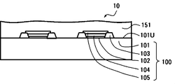
- FIG. 2 is a longitudinal sectional view schematically showing an example of a resin-sealed organic electronics device sealing body made of the assembly and a sealing material layer manufactured by the manufacturing method of the present invention.
- the organic electronic device sealing body 10 includes an assembly 100 and a sealing material layer 151 provided on the upper surface 101U side of the assembly 100.
- the sealing material layer 151 is a sealing material made of a hydrocarbon-based soft resin having an alkoxysilyl group used in the present invention, the moisture barrier property is excellent. As a result, good sealing is achieved and the durability of the device is increased. Furthermore, the unevenness of the assembly 100 is covered by the soft performance of the sealing material, and as a result, the strength of the device can be increased.
- a method for providing the sealing material layer 151 on the assembly 100 a method is adopted in which a sheet-shaped sealing material is superposed on a substrate on which an organic functional element is mounted, and is pressed and pressure-bonded in an autoclave.
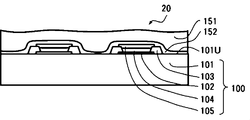
- FIG. 3 is a longitudinal sectional view schematically showing another example of a resin-sealed organic electronic device sealing body manufactured by the manufacturing method of the present invention.
- the organic electronic device sealing body 20 includes an assembly 100, a temporary sealing layer 152 provided on the upper surface 101 U side of the assembly 100, and a sealing material layer provided on the temporary sealing layer 152. 151.
- Examples of the material of the temporary sealing layer 152 include materials containing silicon such as silicon nitride (SiN) and silicon oxide (SiO).
- the temporary sealing layer 152 has a thickness of about 0.2 to 1 ⁇ m.
- the temporary sealing layer 152 can be formed by a film formation method such as vapor deposition under the same conditions as the light emitting layer 104 and the second electrode layer 105 under a reduced pressure environment. By continuously providing the light emitting layer 104, the second electrode layer 105, and the temporary sealing layer 152 in a reduced pressure environment, deterioration of the light emitting layer can be effectively suppressed.
- the sealing body which can endure under the use environment of a device can be obtained by taking out these from the pressure-reduced environment, and sealing with the sealing material layer 151.
- FIG. Thereby, it is possible to obtain a device in which the deterioration of the element at the time of manufacture is small and the state is maintained for a long time even in the use environment.
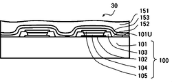
- FIG. 4 is a longitudinal sectional view schematically showing still another example of a resin-sealed organic electronics device sealing body manufactured by the manufacturing method of the present invention.
- the organic electronic device sealing body 30 includes an assembly 100, a temporary sealing layer 152 provided on the upper surface 101U side of the assembly 100, and an adsorbent layer 153 provided on the temporary sealing layer 152. And a sealing material layer 151 provided on the adsorbent layer 153.
- an organoaluminum complex can be given.
- the thickness of the adsorbent layer 153 is about 0.1 to 1 ⁇ m.
- the sealing property can be further strengthened. For example, a gas component that can be slightly released from the sealing material layer 151 can be adsorbed to further prevent deterioration of the light-emitting layer 104 and the like.
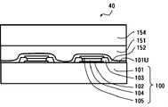
- FIG. 5 is a longitudinal sectional view schematically showing an example of a resin-sealed organic electronics device sealing body made of the assembly, the sealing material layer, and the protective layer, manufactured by the manufacturing method of the present invention. is there.
- the organic electronic device sealing body 40 includes an assembly 100, a sealing material layer 151 provided on the upper surface 101U side of the assembly 100, and a protective layer 154 on the upper surface thereof.
- the light-emitting layer 104 is sealed with the substrate 101, the sealing material layer 151, and the protective layer 154.
- the sealing material layer 151 is a sealing material made of a hydrocarbon-based soft resin having an alkoxysilyl group used in the present invention, the moisture barrier property is excellent. As a result, good sealing is achieved and the durability of the device is increased. Furthermore, the unevenness of the assembly 100 is covered by the soft performance of the sealing material, and as a result, the strength of the device can be increased.
- FIG. 6 is a longitudinal sectional view schematically showing still another example of an organic electronic device sealing body including components such as a resin-sealed organic semiconductor manufactured by the manufacturing method of the present invention.
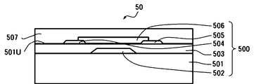
- the organic electronic device sealing body 50 includes an assembly 500 and a sealing material layer 507 provided on the upper surface of the assembly 500.
- the assembly 500 is provided on the top surface of the substrate 501, the gate electrode 502 provided on the top surface of the substrate 501, the gate electrode insulating layer 503 provided on the top surface of the substrate 501 and the gate electrode 502, and the gate electrode insulating layer 503.
- a semiconductor layer 506, a source electrode 504, and a drain electrode 505 are included.
- the material of the element which comprises the organic electronics device sealing body 50, thickness, and a manufacturing method it does not specifically limit but a well-known thing is employable.
- the material of the substrate 501 is not particularly limited, and is a flexible substrate made of a flexible plastic such as polycarbonate, polyimide, polyethylene terephthalate, polyethylene naphthalate, and alicyclic olefin polymer; quartz, soda glass, inorganic alkali glass, Glass substrates such as silicon wafers, silicon carbide wafers, sapphire wafers, compound semiconductor wafers, and the like.
- a flexible plastic such as polycarbonate, polyimide, polyethylene terephthalate, polyethylene naphthalate, and alicyclic olefin polymer
- quartz soda glass
- inorganic alkali glass Glass substrates such as silicon wafers, silicon carbide wafers, sapphire wafers, compound semiconductor wafers, and the like.
- the gate electrode 502 can be formed using a conductive material.
- Conductive materials include platinum, gold, silver, nickel, chromium, copper, iron, tin, antimony lead, tantalum, indium, palladium, tellurium, rhenium, iridium, aluminum, ruthenium, germanium, molybdenum, tungsten, tin oxide, Antimony, indium tin oxide (ITO), fluorine-doped zinc oxide, zinc, carbon, graphite, glassy carbon, silver paste, and carbon paste, lithium, beryllium, magnesium, potassium, calcium, scandium, titanium, manganese, zirconium, Gallium, niobium, sodium, sodium-potassium alloy, magnesium / copper mixture, magnesium / silver mixture, magnesium / aluminum mixture, magnesium / indium mixture, aluminum / aluminum oxide Arm mixtures, and lithium / aluminum mixture and the like.
- a known conductive polymer whose conductivity is improved by doping for example, conductive polyaniline, conductive polypyrrole, conductive polythiophene (polyethylenedioxythiophene and polystyrenesulfonic acid complex, etc.) can also be used as the conductive material. .
- conductive polyaniline conductive polypyrrole
- conductive polythiophene polyethylenedioxythiophene and polystyrenesulfonic acid complex, etc.
- chromium and molybdenum are preferable, and chromium is more preferable.
- the gate electrode 502 is formed in a predetermined pattern on the substrate 501 by, for example, forming the above-described conductive material on the substrate 501 by a sputtering method or the like and then performing an etching process.
- the material of the gate electrode insulating layer 503 is preferably one having sealing properties, moisture resistance, insulation properties, and chemical resistance.
- thermoplastic resins such as polyimide, polyester, polyethylene naphthalate, polycarbonate, polyethylene, polyethylene terephthalate, and polyether sulfone can be exemplified, but the same resin as the sealing material layer 507 can also be used.
- the semiconductor layer 506 can be formed using an organic semiconductor.
- organic semiconductors pentacene, naphthacene, thiophene oligomer, perylene, p-sexiphenyl, and derivatives thereof, naphthalene, anthracene, rubrene and derivatives thereof, coronene, and derivatives thereof, metal-containing / non-containing phthalocyanines And low molecular semiconductors such as derivatives thereof; polymer semiconductors such as polyalkylthiophene based on thiophene and fluorene, polyalkylfluorene and derivatives thereof; and the like.
- the semiconductor layer 506 is formed by, for example, forming the above-described organic semiconductor layer on the gate electrode insulating layer 503 by a coating method, a CVD method, or the like, and then patterning the gate electrode insulating layer 503 into a predetermined pattern shape. Is done.
- the source electrode 504 and the drain electrode 505 can be formed of a conductive material.
- the conductive material the same material as the above-described gate electrode 502 can be used.
- the source electrode 504 and the drain electrode 505 are formed in a predetermined pattern on the semiconductor layer 506 by, for example, forming the above-described conductive material layer on the semiconductor layer 506 by a sputtering method or the like and then performing an etching process. Is done.
- an organic electronic device sealing body 50 as an organic semiconductor includes a sealing material layer 507 provided on the upper surface 501U side of the assembly 500.
- the semiconductor layer 506, the source electrode 504, and the drain electrode 505 are sealed with the gate electrode insulating layer 503 and the sealing material layer 507.
- the sealing material layer 507 is a sealing material layer made of a hydrocarbon-based soft resin having an alkoxysilyl group used in the present invention, the moisture barrier property is excellent. As a result, good sealing is achieved and the durability of the device is increased. Furthermore, the unevenness of the assembly 500 is covered by the soft performance of the sealing material, and as a result, the strength of the device can be increased.
- the sealant used in the present invention is a sheet-like sealant made of a modified hydrocarbon soft resin having an alkoxysilyl group.
- the modified hydrocarbon soft resin having an alkoxysilyl group is one in which an alkoxysilyl group is introduced by reacting a hydrocarbon soft resin with an ethylenically unsaturated silane compound in the presence of an organic peroxide. is there.
- an alkoxysilyl group By introducing an alkoxysilyl group into the hydrocarbon-based soft resin, the hydrocarbon-based soft resin is imparted with strong adhesion to a glass substrate or a plastic substrate.
- the modified hydrocarbon soft resin having an alkoxysilyl group has a storage elastic modulus G ′ in the dynamic viscoelastic property of 25 ° C., usually 1 ⁇ 10 6 Pa to 1 ⁇ 10 9 Pa, preferably 1 ⁇ 10. It is a soft resin of 7 Pa or more and 5 ⁇ 10 8 Pa or less.
- the storage elastic modulus G ′ is measured using a known dynamic viscoelasticity measuring device, for example, a viscoelasticity measuring device (ARES, manufactured by T.A.
- the hydrocarbon-based soft resin used as a raw material for the sealing material used in the present invention includes a polymer block [polymer block (A)] having a structural unit derived from an aromatic vinyl compound as a main component and a chain conjugated diene compound.
- Block copolymer hydride (i) obtained by hydrogenating a block copolymer [block copolymer (C)] comprising a polymer block [polymer block (B)] having a structural unit derived from the main component
- the block copolymer hydride (i) is a polymer obtained by hydrogenating the block copolymer (C).
- the number of polymer blocks (A) in the block copolymer (C) is usually 3 or less, preferably 2 and the number of polymer blocks (B) is usually 2 or less, preferably 1 It is.
- the form of the block of the block copolymer (C) may be a chain type block or a radial type block, but a chain type block is preferred because of its excellent mechanical strength.
- the most preferred form of the block copolymer (C) is a triblock copolymer of the (A)-(B)-(A) type in which the polymer block (A) is bonded to both ends of the polymer block (B). It is.
- the plurality of polymer blocks (A) may be the same as or different from each other.
- the polymer blocks (B) may be the same as or different from each other.
- the molecular weight of the block copolymer (C) is a weight average molecular weight (Mw) in terms of polystyrene measured by gel permeation chromatography (GPC) using tetrahydrofuran (THF) as a solvent, and is usually 30,000 or more. Preferably it is 35,000 or more, More preferably, it is 40,000 or more, Usually 150,000 or less, Preferably it is 100,000 or less, More preferably, it is 70,000 or less. Moreover, it is 30,000 or more and 150,000 or less normally, Preferably it is 35,000 or more and 100,000 or less, More preferably, it is 40,000 or more and 70,000 or less.
- the molecular weight distribution (Mw / Mn) of the block copolymer (C) is preferably 3 or less, more preferably 2 or less, and particularly preferably 1.5 or less. When Mw and Mw / Mn are within the above ranges, a sealing material with good sealing properties and mechanical strength can be obtained.
- the block copolymer (C) has a ratio wA: wB of wA: wB of 20: 80-60: 40, preferably 25: 75-55: 45, more preferably 30: 70-50: 50. is there. If the ratio wA: wB is within this range, a sealing material having good sealing properties and heat resistance can be obtained.
- the polymer block (A) of the block copolymer (C) is mainly composed of an aromatic vinyl compound, and the content of the structural unit derived from the aromatic vinyl compound in the polymer block (A) is Usually, it is 95% by weight or more, preferably 97% by weight or more, more preferably 99% by weight or more.
- the polymer block (A) can contain a structural unit derived from a chain conjugated diene and / or a structural unit derived from another vinyl compound as a component other than the structural unit derived from the aromatic vinyl compound.
- the content is usually 5% by weight or less, preferably 3% by weight or less, more preferably 1% by weight or less.
- aromatic vinyl compound examples include styrene, 2-methylstyrene, 3-methylstyrene, 4-methylstyrene, 2,4-diisopropylstyrene, 2,4-dimethylstyrene, 4-t-butylstyrene, Examples thereof include 5-t-butyl-2-methylstyrene, 4-monochlorostyrene, dichlorostyrene, 4-monofluorostyrene, 4-phenylstyrene and the like. Among them, those having no polar group are preferable in terms of low dielectric constant and low hygroscopicity, and styrene is particularly preferable from the viewpoint of industrial availability.
- chain conjugated diene and other vinyl compounds that can be copolymerized examples include those similar to the chain conjugated diene and other vinyl compounds that form the structural unit of the polymer block (B) described later.
- the polymer block (B) is mainly composed of a chain conjugated diene compound, and the content of the structural unit derived from the chain conjugated diene compound in the polymer block (B) is usually 95% by weight or more, Preferably it is 97 weight% or more, More preferably, it is 99 weight% or more.
- Components other than the structural unit derived from the chain conjugated diene compound in the polymer block (B) may include a structural unit derived from an aromatic vinyl compound and / or a structural unit derived from another vinyl compound. Its content is usually 5% by weight or less, preferably 3% by weight or less, more preferably 1% by weight or less.
- chain conjugated diene compound examples include 1,3-butadiene, isoprene, 2,3-dimethyl-1,3-butadiene, 1,3-pentadiene and the like.
- a chain conjugated diene compound containing no polar group is preferred from the viewpoint of hygroscopicity, and 1,3-butadiene and isoprene are particularly preferred from the viewpoint of industrial availability.
- vinyl compounds include chain vinyl compounds, cyclic vinyl compounds, unsaturated cyclic acid anhydrides, unsaturated imide compounds, and the like. These compounds may have a substituent such as a nitrile group, an alkoxycarbonyl group, a hydroxycarbonyl group, or a halogen atom.
- the block copolymer hydride (i) is a polymer obtained by hydrogenating the block copolymer (C).
- the hydrogenation rate thereof Is usually 90% or more, preferably 97% or more, more preferably 99% or more. As the hydrogenation rate is higher, a sealing material having better oxidation resistance and light resistance can be obtained.
- the block copolymer hydride (i) is obtained by hydrogenating the carbon-carbon unsaturated bond of the main chain and the side chain of the block copolymer (C) and the carbon-carbon unsaturated bond of the aromatic ring.
- the hydrogenation rate of the carbon-carbon unsaturated bonds in the main chain and the side chain is usually 90% or higher, preferably 97% or higher, more preferably 99% or higher.
- the hydrogenation rate of the carbon unsaturated bond is usually 90% or more, preferably 97% or more, more preferably 99% or more.
- the hydrogenation rate of all unsaturated bonds (carbon-carbon unsaturated bonds in the main and side chains and carbon-carbon unsaturated bonds in the aromatic ring) of the block copolymer (C) is usually 90% or more, preferably Is 97% or more, more preferably 99% or more. As the hydrogenation rate is higher, a sealing material having better oxidation resistance and light resistance can be obtained.
- the hydrogenation rate of the block copolymer hydride (i) can be determined by measuring 1 H-NMR of the block copolymer hydride (ia).
- the block copolymer hydride (i) can be produced according to a known method.
- Block copolymer hydride obtained by selectively hydrogenating only the non-aromatic carbon-carbon unsaturated bonds in the main chain and side chain of a polymer block mainly composed of a structural unit derived from a chain conjugated diene compound (ip ) Can be produced, for example, according to the methods described in JP-A-59-133203, JP-A-60-079005, JP-A-61-028507, and the like.
- the aromaticity and non-aromaticity of the main chain and side chain of the polymer block mainly composed of a structural unit derived from an aromatic vinyl compound and the polymer block mainly composed of a structural unit derived from a chain conjugated diene compound
- the block copolymer hydride (ia) obtained by hydrogenating a carbon-carbon unsaturated bond of a family is, for example, a method described in WO 1996/34896 pamphlet, WO 2003/018656 pamphlet, WO 2012/043708 pamphlet, etc. Can be manufactured according to.
- the block copolymer hydride (i) is a block copolymer in which both aromatic and non-aromatic carbon-carbon unsaturated bonds in the main chain and side chain are hydrogenated from the viewpoint of light resistance and heat resistance. Polymer hydrides (ia) are preferred.
- block copolymer hydrides ia
- at least two polymer blocks (A) mainly comprising a structural unit derived from an aromatic vinyl compound from the viewpoint of sealing properties and heat resistance of the organic electronic device
- a block copolymer (C) comprising a structural unit derived from a chain conjugated diene compound as a main component and comprising at least one polymer block (B), wherein the entire polymer block (A) is a block copolymer.
- Block weight Body hydride is more preferable.
- Block copolymer hydride produced by hydrogenating 90% or more of carbon-carbon unsaturated bonds in the main chain and side chain and carbon-carbon unsaturated bonds in the aromatic ring of block copolymer (C) in this range Since (ia) has flexibility, the obtained sealing material can reduce damage to the organic EL element and the like.
- the molecular weight of the block copolymer hydride (i) is a polystyrene-equivalent weight average molecular weight (Mw) measured by GPC using THF as a solvent, and is usually 30,000 or more, preferably 35,000 or more, more preferably. It is 40,000 or more, usually 150,000 or less, preferably 100,000 or less, more preferably 70,000 or less. Moreover, it is 30,000 or more and 150,000 or less normally, Preferably it is 35,000 or more and 100,000 or less, More preferably, it is 40,000 or more and 70,000 or less.
- Mw polystyrene-equivalent weight average molecular weight measured by GPC using THF as a solvent
- the molecular weight distribution (Mw / Mn) of the block copolymer hydride (i) is preferably 3 or less, more preferably 2 or less, and particularly preferably 1.5 or less. When Mw and Mw / Mn are within the above ranges, a sealing material with good sealing properties and mechanical strength can be obtained.
- Polyolefin resin (ii) As the polyolefin resin (ii), a (co) polymer having a melting point of 90 ° C. or more and 140 ° C. or less obtained by polymerizing ethylene and / or an ⁇ -olefin having 3 to 10 carbon atoms can be used.
- the ⁇ -olefin having 3 to 10 carbon atoms include propylene, 1-butene, 1-pentene, 1-hexene, 1-heptene, 1-octene, 4-methyl-1-pentene, vinylcyclohexane, and the like. These can be used individually by 1 type or in combination of 2 or more types.
- the method for synthesizing the polyolefin is not particularly limited, and a general method is employed.
- the melting point is 90 ° C. or more and 140 ° C. or less, preferably 100 ° C., among commercially available polyolefins produced using one or more olefins selected from the group consisting of ethylene and ⁇ -olefins having 3 to 10 carbon atoms.
- a material having a temperature not lower than 130 ° C and not higher than 130 ° C can be selected and used.
- a polyolefin having a melting point of less than 90 ° C. is used, the heat resistance as a sealing material for organic electronics devices is inferior.
- the sealing method for organic electronics devices of the present invention There is a possibility that the sealing performance is inferior.
- polyolefins that can be used include low density polyethylene, high density polyethylene, ethylene / vinyl acetate copolymer, polypropylene, ethylene / propylene copolymer, ethylene / octene copolymer, poly-4-methylpentene, and the like. It is done.
- Modified hydrocarbon soft resin having alkoxysilyl group The modified hydrocarbon soft resin having an alkoxysilyl group reacts a block copolymer hydride (i) and / or a polyolefin resin (ii) with an ethylenically unsaturated silane compound in the presence of an organic peroxide. Can be manufactured.
- alkoxysilyl group to be introduced examples include tri (C1-C6 alkoxy) silyl groups such as trimethoxysilyl group and triethoxysilyl group; methyldimethoxysilyl group, methyldiethoxysilyl group, ethyldimethoxysilyl group, ethyl (C1-C20 alkyl) di (C1-C6 alkoxy) silyl group such as diethoxysilyl group, propyldimethoxysilyl group, propyldiethoxysilyl group; phenyldimethoxysilyl group, phenyldiethoxysilyl group, etc.
- tri (C1-C6 alkoxy) silyl groups such as trimethoxysilyl group and triethoxysilyl group
- alkoxysilyl group may be bonded to the hydrocarbon-based soft resin via a divalent organic group such as an alkylene group having 1 to 20 carbon atoms or an alkyleneoxycarbonylalkylene group having 2 to 20 carbon atoms. good.
- the introduction amount of the alkoxysilyl group into the hydrocarbon soft resin is usually 0.1 parts by weight or more, preferably 0.2 parts by weight or more, more preferably 0.5 parts by weight with respect to 100 parts by weight of the hydrocarbon soft resin.
- the amount is usually 10 parts by weight or less, preferably 5 parts by weight or less, more preferably 3 parts by weight or less.
- it is 0.1 to 10 weight part normally, Preferably it is 0.2 to 5 weight part, More preferably, it is 0.5 to 3 weight part.
- the resulting modified hydrocarbon-based soft resin undergoes cross-linking between alkoxysilyl groups decomposed with a small amount of moisture during storage, gelling, and fluidity during melt molding Or the adhesiveness as a sealing material may be reduced.
- substrate of an organic electronics device may fall.
- the ethylenically unsaturated silane compound to be used is not particularly limited as long as it is graft-polymerized with a hydrocarbon soft resin to introduce an alkoxysilyl group into the hydrocarbon soft resin.
- vinyltrimethoxysilane, vinyltriethoxysilane, allyltrimethoxysilane, allyltriethoxysilane, dimethoxymethylvinylsilane, diethoxymethylvinylsilane, p-styryltrimethoxysilane, 3-acryloxypropyltrimethoxysilane, 3-acrylic Loxypropyltriethoxysilane, 3-methacryloxypropyltrimethoxysilane, 3-methacryloxypropyltriethoxysilane, 3-methacryloxypropylmethyldimethoxysilane, 3-methacryloxypropylmethyldiethoxysilane, 3-acryloxypropyltrimethoxy Silane and the like are preferably used.
- ethylenically unsaturated silane compounds may be used alone or in combination of two or more.
- the amount of the ethylenically unsaturated silane compound used is usually 0.1 parts by weight or more, preferably 0.2 parts by weight or more, more preferably 0.5 parts by weight or more with respect to 100 parts by weight of the hydrocarbon soft resin.
- the amount is usually 10 parts by weight or less, preferably 5 parts by weight or less, more preferably 3 parts by weight or less.
- it is 0.1 to 10 weight part normally, Preferably it is 0.2 to 5 weight part, More preferably, it is 0.5 to 3 weight part.
- the peroxide those having a one-minute half-life temperature of 170 ° C. or higher and 190 ° C. or lower are preferably used.
- t-butyl cumyl peroxide, dicumyl peroxide, di-t-hexyl peroxide, 2,5-dimethyl-2,5-di (t-butylperoxy) hexane, di-t-butyl peroxide, Di (2-t-butylperoxyisopropyl) benzene or the like is preferably used.
- These peroxides may be used alone or in combination of two or more.
- the amount of the peroxide used is usually 0.05 to 2 parts by weight, preferably 0.1 to 1 part by weight, more preferably 0. 2 parts by weight or more and 0.5 parts by weight or less.
- the method for reacting the hydrocarbon soft resin and the ethylenically unsaturated silane compound in the presence of a peroxide is not particularly limited.
- an alkoxysilyl group can be introduced into the hydrocarbon-based soft resin by kneading for a desired time at a desired temperature in a biaxial kneader.
- the kneading temperature by the biaxial kneader is usually 180 ° C. or higher and 220 ° C. or lower, preferably 185 ° C. or higher and 210 ° C. or lower, more preferably 190 ° C. or higher and 200 ° C. or lower.
- the heating and kneading time is usually about 0.1 to 10 minutes, preferably about 0.2 to 5 minutes, more preferably about 0.3 to 2 minutes. What is necessary is just to knead
- the form of the produced modified hydrocarbon soft resin having an alkoxysilyl group is not limited, it can be usually made into a pellet shape and used for the subsequent production of the sealing material.
- the sealing material used in the present invention contains the above-described modified hydrocarbon soft resin as a main component.
- the content of the modified hydrocarbon soft resin in the sealing material used in the present invention is usually 70% by weight or more, preferably 75% by weight or more, more preferably 80% by weight or more with respect to the sealing material. .
- additives can be blended in addition to the modified hydrocarbon soft resin as a main component.
- Additives that can be blended include a softening agent for adjusting the adhesive temperature and adhesion to the device and the substrate, an antioxidant and a light stabilizer for improving durability, and the like.
- the softener can be blended with the modified hydrocarbon soft resin to adjust the flexibility of the sealing material to a preferable range.
- the softening agent those that can be uniformly dissolved or dispersed in the modified hydrocarbon soft resin are preferable, and hydrocarbon polymers having a low molecular weight (number average molecular weight of 300 to 5,000) are preferable.
- hydrocarbon polymer examples include polyisobutylene, polybutene, poly-4-methylpentene, poly-1-octene, low molecular weight compounds such as ethylene / ⁇ -olefin copolymer and hydrides thereof; polyisoprene, Examples thereof include low molecular weight substances (number average molecular weights of 300 to 5,000) such as polyisoprene-butadiene copolymers and hydrides thereof.
- a softener can be used individually by 1 type or in combination of 2 or more types.
- a low molecular weight polyisobutylene hydride and a low molecular weight polyisoprene hydride are particularly preferable in terms of maintaining transparency and light resistance and being excellent in softening effect.
- the blending amount of the softening agent is usually 25 parts by weight or less, preferably 20 parts by weight or less, more preferably 15 parts by weight or less with respect to 100 parts by weight of the hydrocarbon soft resin.
- the blending amount of the softening agent is usually 25 parts by weight or less, preferably 20 parts by weight or less, more preferably 15 parts by weight or less with respect to 100 parts by weight of the hydrocarbon soft resin.
- antioxidant and light stabilizer phosphorus antioxidants, phenol antioxidants, sulfur antioxidants, hindered amine light stabilizers and the like can be used. These antioxidants and light stabilizers can be used alone or in combination of two or more.
- the compounding amount of the additive is usually 3 parts by weight or less, preferably 2 parts by weight or less, more preferably 1 part by weight or less with respect to 100 parts by weight of the modified hydrocarbon soft resin.
- a known method generally used as a method for producing a resin composition can be applied.
- the modified hydrocarbon soft resin and additives are mixed evenly using a mixer such as a tumbler mixer, ribbon blender, Henschel type mixer, etc., and then melted by a continuous melt kneader such as a twin screw extruder.
- a modified hydrocarbon soft resin blended with an additive can be produced by mixing and extruding into a pellet.
- the sealing material used in the present invention is formed into a sheet prior to use.
- the thickness of the sheet is preferably 10 ⁇ m or more and 200 ⁇ m or less, more preferably 20 ⁇ m or more and 100 ⁇ m or less, and particularly preferably 30 ⁇ m or more and 50 ⁇ m or less.
- the sheet-like sealing material is usually prepared as a long sheet, and the organic electronic device is sealed using this sheet.
- the method for producing the sheet is not particularly limited, and the sheet is usually formed by a melt extrusion molding method.
- the “long” means a sheet having a length of at least about 5 times the width direction of the sheet, preferably a length of 10 times or more, for example, in a roll shape. It has a length that can be wound and stored or transported.
- Process [1] in the manufacturing method of the organic electronics device sealing body of the present invention is a process of stacking an organic electronics device and a sheet-shaped sealing material to produce a laminate.
- the laminate can be obtained by stacking a sheet-like sealing material on the surface on which the organic functional element of the organic electronic device before resin sealing is disposed so that the organic functional element is completely covered.
- a transparent glass sheet, a transparent plastic sheet, or the like as a barrier layer can be further stacked.
- Step [2] in the method for producing an organic electronic device sealed body of the present invention includes the step of storing the laminate produced in Step [1] inside a resin bag and degassing the inside of the resin bag. This is a step of sealing the resin bag containing the laminate.
- the resin bag used in the sealing method of the present invention may be any bag as long as the opening can be sealed by heat sealing or the like after accommodating the laminate and degassing the inside.
- Examples of the resin constituting the bag include polyethylene (PE), polypropylene (PP), polyethylene terephthalate (PET), nylon (NY), and the like.
- the resin bag may have a single layer structure or a multilayer structure.
- the layer structure of the multilayer bag include PET layer / adhesive layer / PE layer, PET layer / adhesive layer / PP layer, NY layer / adhesive layer / PE layer, NY layer / adhesive layer / PP layer, PET Layer / adhesive layer / NY layer / adhesive layer / PP layer, and the like.
- the composition is preferable because it has high heat resistance and can increase the molding temperature of the organic electronic device, and the NY layer / adhesive layer / PP layer is particularly preferable because it has excellent puncture resistance.
- the thickness of the resin bag is usually 30 ⁇ m or more and 200 ⁇ m or less, preferably 40 ⁇ m or more and 150 ⁇ m or less, and more preferably 50 ⁇ m or more and 100 ⁇ m or less in both cases of a single layer structure and a multilayer structure.
- the thickness of each layer in the case of a multilayer structure is not particularly limited and may be appropriately selected.
- a thin film having a thickness of 100 ⁇ m or less is used.
- a resin-made bag that can be sealed a commercially available bag for a vacuum pack of food or the like can be used.
- step [2] (a) First, a laminate in which the organic electronic device produced in the step [1] and a sheet-like sealing material, and if necessary, a glass sheet or a plastic sheet as a barrier layer are stacked, It is accommodated inside the resin bag.
- a laminate in which the organic electronic device produced in the step [1] and a sheet-like sealing material, and if necessary, a glass sheet or a plastic sheet as a barrier layer are stacked, It is accommodated inside the resin bag.
- accommodation the laminate inside the bag an aspect of putting the laminate into the bag from the opening of the resin bag, placing the laminate on one resin sheet, After covering another resin sheet thereon, the outer peripheral portion of the two resin sheets is heat-sealed leaving an opening, and as a result, the laminate is accommodated in the bag.
- a method for degassing the inside of the bag is not particularly limited, and examples thereof include a method using a vacuum pump, a suction pump, or the like.
- the bag whose inside is deaerated is sealed.
- the method of sealing is not specifically limited, The method of using a heat sealer, an infrared welder, an ultrasonic welder, etc. is mentioned. Moreover, a commercially available vacuum packer, a vacuum packaging machine, etc. can also be used.
- Step [3] in the method for producing an organic electronic device encapsulant of the present invention is a method in which a bag containing the laminate prepared in step [2] and sealed is pressurized and heated to bond and integrate the laminate. This is a process for manufacturing an organic electronic device sealed with a stopper.
- the sealed bag containing the laminate is usually 0.1 MPa or more, preferably 0.1 MPa or more and 2.0 MPa or less, more preferably 0.2 MPa or more and 1.5 MPa or less, and still more preferably. Is placed under pressure of 0.4 MPa or more and 1.0 MPa or less. If it is the pressure of this range, since the autoclave currently sold for the manufacture of a laminated glass etc. can be utilized, it is preferable.
- the heating temperature is within the range of the temperature that the organic functional element to be sealed can withstand or the temperature of the material of the resin bag.
- the heating temperature depends on the type of organic functional element to be sealed and the type of resin bag, but is usually 80 ° C. or higher and 150 ° C. or lower, preferably 90 ° C. or higher and 140 ° C. or lower, more preferably 100 ° C. or higher and 130 ° C. It is as follows.
- the pressure or the pressure heating time is usually 10 to 100 minutes, preferably 15 to 70 minutes, more preferably 20 to 40 minutes, depending on conditions and the like.
- an organic electronic device sealed with a sealing material with few defects such as remaining bubbles and poor adhesion and excellent sealing performance can be easily produced.
- the method of pressurizing or heating under pressure is not particularly limited, a method using an autoclave, a heat-pressure curing apparatus, a steam sterilization apparatus or the like is preferable. When these pressurization apparatuses are used, since a large number of organic electronic devices can be filled in the apparatus at a time for sealing treatment, industrial productivity is excellent.
- the resin bag can be taken out from the pressure device or the like, and the organic electronic device sealing body sealed with the sealing material can be taken out from the resin bag and can be used.
- the packaging for protecting the organic electronics device encapsulant sealed with the encapsulant is omitted, and the product is handled while sealed in a resin bag. It is also effective for cost reduction.
- Evaluation in this example is performed by the following method.
- Mw Weight average molecular weight
- Mw / Mn molecular weight distribution
- the molecular weights of the block copolymer and the hydride of the block copolymer were measured at 38 ° C. as standard polystyrene equivalent values by GPC using THF as an eluent.
- THF as an eluent.
- HLC8020GPC manufactured by Tosoh Corporation was used.
- Hydrogenation rate The hydrogenation rate of the main chain, side chain and aromatic ring of the block copolymer hydride was calculated by measuring a 1 H-NMR spectrum.
- Assembly (1) including a white organic EL element The structure of the assembly with a temporary sealing layer (1) including the white organic EL element is roughly a structure including the assembly 100 and the temporary sealing layer 152 shown in FIG. However, not only one light emitting layer but also a hole transport layer, a plurality of light emitting layers, an electron transport layer, and a buffer layer were provided between the first electrode and the second electrode.
- An ITO layer was formed by vapor deposition (under reduced pressure of 10 ⁇ 4 Pa) on a glass substrate 101 having a light transmittance of 110 mm in length, 65 mm in width, and 0.7 mm in thickness.
- This ITO layer was formed by photolithography to form a strip shape having a thickness of 0.25 ⁇ m, a width of 500 ⁇ m, and a length of 10 mm, and a transparent anode as the first electrode layer 102 was formed.
- a photoresist (trade name: ZWD6216, manufactured by Nippon Zeon Co., Ltd.) was applied and photolithography was performed to form an edge cover layer 103 having a thickness of 1.0 ⁇ m around the anode.
- a photoresist (trade name: ZWD6216, manufactured by Nippon Zeon Co., Ltd.) was applied and photolithography was performed to form an edge cover layer 103 having a thickness of 1.0 ⁇ m around the anode.
- NPB 4,4′-bis [N- (1-naphthyl) -N-phenylamino] biphenyl
- red light emitting material 4- (dicyanomethylene) -2-t-butyl-6- (1,1,7,7-tetramethyljuridyl-9-enyl)- 4H-pyran (DCJTB) was deposited to form a red light emitting layer having a thickness of 0.05 ⁇ m.
- tris (8-hydroxyquinolinato) aluminum Alq3 was vapor-deposited on the red light emitting layer to form a 0.05 ⁇ m thick green light emitting layer and an electron transport layer. Further, LiF was evaporated on the electron transport layer to form a buffer layer having a thickness of 0.5 nm.
- aluminum was deposited on the buffer layer to form a cathode (reflective electrode) having a thickness of 50 nm as the second electrode layer 105.
- silicon nitride (SiN) was vapor-deposited so that the formed layer and the whole substrate might be covered, and the temporary sealing layer 152 with a thickness of 0.3 micrometer was formed. Vapor deposition from the hole transport layer to the temporary sealing layer was continued while maintaining the pressure of 10 ⁇ 4 to 10 ⁇ 6 Pa.
- a sheet (thickness 20 ⁇ m) of the sealing material (1) was extruded under molding conditions of a molten resin temperature of 180 ° C., a T die temperature of 180 ° C., and a cast roll temperature of 40 ° C.
- the sheet of the sealing material (1) and the PET for releasability are supplied to the sheet surface of the sealing material (1) extruded onto the cast roll while supplying the PET film for release (thickness 50 ⁇ m).
- the film was piled up and wound up and collected on a roll.
- Sealing material (2) Modified polyolefin (ii1-s) Vinyl trimethoxysilane (KBM-1003, Shin-Etsu Chemical Co., Ltd.) per 100 parts of a commercially available ethylene / octene copolymer (product name “Affinity (registered trademark) PL1880”, melting point 100 ° C., manufactured by Dow Chemical Japan)) 2.0 parts) and 2,5-dimethyl-2,5-di (t-butylperoxy) hexane (product name [Perhexa (registered trademark) 25B], manufactured by NOF Corporation) are added. did. This mixture was kneaded using a twin screw extruder at a resin temperature of 200 ° C. and a residence time of 80 to 90 seconds to produce 95 parts of pellets of modified polyolefin (ii1-s) having alkoxysilyl groups.
- a commercially available ethylene / octene copolymer product name “Affinity (registere
- the FT-IR spectrum of the resulting modified polyolefin (ii1-s) pellet was measured, and a new absorption band derived from Si—OCH 3 group at 1090 cm ⁇ 1 and Si—CH 2 group at 825 and 739 cm ⁇ 1. Were observed at positions different from those 1075, 808, 766 cm ⁇ 1 of vinyltrimethoxysilane. Further, it was estimated from the IR absorbance value that about 1.9 parts of vinyltrimethoxysilane was introduced into 100 parts of the ethylene / octene copolymer.
- Sheet of sealing material (2) Except for using modified polyolefin (ii1-s) pellets, a ratio of 5 parts hydrogenated polybutene to 100 parts modified polyolefin (ii1-s), molten resin temperature 150 ° C., T-die temperature 150 ° C. In the same manner as in Production Example 2, a sheet of sealing material (2) (thickness 20 ⁇ m) is extruded, and the obtained sheet of sealing material (2) and a PET film for releasability are overlapped and rolled up and collected. did.
- Sealing material (3) Modified block copolymer hydride (ip2-s)
- a commercially available block copolymer partially hydride product name “Tuftec (registered trademark) H1051”, styrene / ethylene / butylene ratio: 42/58 (weight ratio), manufactured by Asahi Kasei Chemicals
- vinyl 2.0 parts of trimethoxysilane and 0.2 part of 2,5-dimethyl-2,5-di (t-butylperoxy) hexane were added and mixed uniformly.
- This mixture was kneaded using a twin screw extruder at a resin temperature of 200 ° C. and a residence time of 80 to 90 seconds, and 95 parts of a pellet of partially modified block copolymer partially hydride (ip2-s) having an alkoxysilyl group.
- Example 1 A sheet of the sealing material (1) having a thickness of 20 ⁇ m produced in Production Example 2 is applied to the surface of the assembly with temporary sealing layer (1) obtained in Production Example 1 on the temporary sealing layer side. Peeled and stacked. A glass sheet having a thickness of 0.7 mm was further stacked thereon as a protective layer to obtain a laminate.
- This laminate was put in a resin bag having a layer structure of NY / adhesive layer / PP and having a thickness of 75 ⁇ m. Heat seal both sides with a heat sealer leaving 200mm width at the center of the opening of the bag, then heat the opening using a sealed pack device (BH-951, manufactured by Panasonic Corporation) while degassing the inside of the bag The laminate was sealed and sealed.
- a sealed pack device BH-951, manufactured by Panasonic Corporation
- an organic EL device sealing body (1) having a structure schematically shown in FIG. 5 and having the assembly 100, the temporary sealing layer 152, the sealing material layer 151, and the protective layer 154 was produced.
- the manufactured organic EL device sealing body (1) was energized, and it was confirmed that the organic EL element was lit without problems. Then, as a result of storing the organic EL device (1) in a non-lighting state in a high temperature and high humidity environment and evaluating the durability, no dark spots were generated and the durability was good ((). .
- Example 2 Except for using the sheet of the sealing material (2) produced in Production Example 3, it has the structure schematically shown in FIG. 5 in the same manner as in Example 1, and includes an assembly 100, a temporary sealing layer 152, An organic EL device sealing body (2) having a sealing material layer 151 and a protective layer 154 was produced.
- Example 1 As in Example 1, the assembly with temporary sealing layer (1) obtained in Production Example 1 and the 20 ⁇ m thick sealing material (1) produced in Production Example 2 on the surface on the temporary sealing layer side A sheet and a 0.7 mm thick glass sheet as a protective layer were stacked to obtain a laminate.
- This laminate was vacuum degassed for 5 minutes at a temperature of 90 ° C. using a vacuum laminator (PVL0202S, manufactured by Nisshinbo Mechatronics), and further pressed for 20 minutes.
- PVL0202S vacuum laminator
- An organic EL device sealing body (3) having a structure schematically shown in FIG.
- the manufactured organic EL device sealing body (3) was energized, and it was confirmed that the organic EL element was lit without problems. Thereafter, the durability was evaluated in the same manner as in Example 1. As a result, a plurality of dark spots having a diameter of 200 ⁇ m or more were generated near the end of the organic EL device, and the durability was poor (x). Further, in the organic EL device sealing body (3) after durability evaluation, sink marks were observed on the inner side of the end portion of the sealing material layer from the end portion of the glass sheet.
- Example 2 As in Example 2, the assembly with temporary sealing layer (1) obtained in Production Example 1, and the sealing material (2) having a thickness of 20 ⁇ m produced in Production Example 3 on the surface on the temporary sealing layer side. A sheet and a 0.7 mm thick glass sheet as a protective layer were stacked to obtain a laminate.
- Example 3 Except for using the sheet of the sealing material (3) prepared in Production Example 4, it has the structure schematically shown in FIG. 5 in the same manner as in Example 1, and includes an assembly 100, a temporary sealing layer 152, An organic EL device sealing body (5) having a sealing material layer 151 and a protective layer 154 was produced.
- the produced organic EL device sealing body (5) was energized, and it was confirmed that the organic EL element was lit without problems. Thereafter, the durability was evaluated in the same manner as in Example 1. As a result, dark spots with a diameter of 50 ⁇ m or more and less than 200 ⁇ m were generated, but the number was small (less than 10 / cm 2 ), and the durability was acceptable ( ⁇ ). It was evaluated.
- the organic functional element was sealed more satisfactorily by sealing the sheet of the sealing material made of the modified hydrocarbon-based soft resin having an alkoxysilyl group and the organic electronics device, and heating and pressing in the autoclave.
- An organic electronic device encapsulant is manufactured.
- the manufactured organic electronic device sealed body maintains its function even after long-term storage in a high temperature and high humidity environment (Examples 1 to 3).
- the manufacturing method of the organic electronics device sealing body of the present invention is an industrial manufacturing method of an organic electronics device having excellent durability using a sealing material made of a resin having excellent sealing performance of an organic functional element. Useful.
- the organic electronic device sealing body manufactured by the manufacturing method of the present invention is excellent in durability.
- Organic electronics device sealing body 20 Organic electronics device sealing body 30: Organic electronics device sealing body 40: Organic electronics device sealing body 50: Organic electronics device sealing body 100: Assembly 101: Substrate 101U: Substrate 102: First electrode layer 103: Edge cover layer 104: Light emitting layer 105: Second electrode layer 151: Sealing material layer 152: Temporary sealing layer 153: Adsorbent layer 154: Protective layer 500: Assembly 501: Substrate 501U: Upper surface of assembly 502: Gate electrode 503: Gate electrode insulation Layer 504: Source electrode 505: Drain electrode 506: Semiconductor layer 507: Layer of sealing resin composition
Landscapes
- Chemical & Material Sciences (AREA)
- Engineering & Computer Science (AREA)
- Organic Chemistry (AREA)
- Materials Engineering (AREA)
- Manufacturing & Machinery (AREA)
- Physics & Mathematics (AREA)
- Optics & Photonics (AREA)
- Health & Medical Sciences (AREA)
- Medicinal Chemistry (AREA)
- Polymers & Plastics (AREA)
- Chemical Kinetics & Catalysis (AREA)
- Inorganic Chemistry (AREA)
- Electroluminescent Light Sources (AREA)
- Addition Polymer Or Copolymer, Post-Treatments, Or Chemical Modifications (AREA)
Abstract
Priority Applications (5)
| Application Number | Priority Date | Filing Date | Title |
|---|---|---|---|
| EP17766589.0A EP3432690B1 (fr) | 2016-03-18 | 2017-03-13 | Procédé de fabrication de corps d'étanchéité de dispositif électronique organique |
| KR1020187026231A KR20180121911A (ko) | 2016-03-18 | 2017-03-13 | 유기 일렉트로닉스 디바이스 봉지체의 제조 방법 |
| US16/080,750 US10553818B2 (en) | 2016-03-18 | 2017-03-13 | Method for manufacturing organic electronic device sealing body |
| JP2018505905A JPWO2017159589A1 (ja) | 2016-03-18 | 2017-03-13 | 有機エレクトロニクスデバイス封止体の製造方法 |
| CN201780014641.4A CN108781492B (zh) | 2016-03-18 | 2017-03-13 | 有机电子器件密封体的制造方法 |
Applications Claiming Priority (2)
| Application Number | Priority Date | Filing Date | Title |
|---|---|---|---|
| JP2016055259 | 2016-03-18 | ||
| JP2016-055259 | 2016-03-18 |
Publications (1)
| Publication Number | Publication Date |
|---|---|
| WO2017159589A1 true WO2017159589A1 (fr) | 2017-09-21 |
Family
ID=59850286
Family Applications (1)
| Application Number | Title | Priority Date | Filing Date |
|---|---|---|---|
| PCT/JP2017/009892 Ceased WO2017159589A1 (fr) | 2016-03-18 | 2017-03-13 | Procédé de fabrication de corps d'étanchéité de dispositif électronique organique |
Country Status (6)
| Country | Link |
|---|---|
| US (1) | US10553818B2 (fr) |
| EP (1) | EP3432690B1 (fr) |
| JP (1) | JPWO2017159589A1 (fr) |
| KR (1) | KR20180121911A (fr) |
| CN (1) | CN108781492B (fr) |
| WO (1) | WO2017159589A1 (fr) |
Cited By (4)
| Publication number | Priority date | Publication date | Assignee | Title |
|---|---|---|---|---|
| WO2019151079A1 (fr) * | 2018-01-31 | 2019-08-08 | 日本ゼオン株式会社 | Film de résine, et dispositif électroluminescent organique |
| WO2019159830A1 (fr) * | 2018-02-16 | 2019-08-22 | 三井化学株式会社 | Matériau d'étanchéité pour dispositif d'affichage d'images et feuille d'étanchéité pour dispositif d'affichage d'images |
| JP2022146935A (ja) * | 2021-03-22 | 2022-10-05 | クレイトン・ポリマーズ・リサーチ・ベー・フェー | シラン官能化スチレンブロックコポリマー |
| US11970606B2 (en) | 2018-01-31 | 2024-04-30 | Zeon Corporation | Resin composition, resin film and organic electroluminescent device |
Families Citing this family (1)
| Publication number | Priority date | Publication date | Assignee | Title |
|---|---|---|---|---|
| US11098865B2 (en) | 2020-05-26 | 2021-08-24 | Korea Photonics Technology Institute | Light source, solar cell complex and lighting system including the same |
Citations (6)
| Publication number | Priority date | Publication date | Assignee | Title |
|---|---|---|---|---|
| JP2002324667A (ja) * | 2001-02-21 | 2002-11-08 | Semiconductor Energy Lab Co Ltd | 発光装置、電子機器およびそれらの作製方法 |
| JP2007115491A (ja) * | 2005-10-19 | 2007-05-10 | Toshiba Matsushita Display Technology Co Ltd | 有機el装置の製造方法 |
| JP2013021064A (ja) * | 2011-07-08 | 2013-01-31 | Institute Of National Colleges Of Technology Japan | 有機膜を含んだ積層体の製造方法、積層体 |
| JP2013062094A (ja) * | 2011-09-13 | 2013-04-04 | Konica Minolta Holdings Inc | 有機エレクトロルミネッセンスパネルおよびその製造方法 |
| WO2014077267A1 (fr) * | 2012-11-15 | 2014-05-22 | 日本ゼオン株式会社 | Composition de résine et article moulé la comprenant |
| WO2014091941A1 (fr) * | 2012-12-10 | 2014-06-19 | 日本ゼオン株式会社 | Composition de résine pour le scellement de dispositifs électroniques organiques et dispositif électronique organique |
Family Cites Families (15)
| Publication number | Priority date | Publication date | Assignee | Title |
|---|---|---|---|---|
| JPS59133203A (ja) | 1983-01-20 | 1984-07-31 | Asahi Chem Ind Co Ltd | 重合体の水添方法 |
| JPS6079005A (ja) | 1983-10-07 | 1985-05-04 | Asahi Chem Ind Co Ltd | リビングポリマ−の水添方法 |
| JPS6128507A (ja) | 1984-07-18 | 1986-02-08 | Asahi Chem Ind Co Ltd | オレフイン性不飽和ポリマ−の水添方法 |
| JPH01134334A (ja) * | 1987-11-19 | 1989-05-26 | Matsushita Electric Ind Co Ltd | 液晶表示装置の製造方法 |
| JPH02164747A (ja) * | 1988-12-19 | 1990-06-25 | Takeda Chem Ind Ltd | 合せガラスの製造法 |
| US5612422A (en) | 1995-05-04 | 1997-03-18 | The Dow Chemical Company | Process for hydrogenating aromatic polymers |
| EP1422253A1 (fr) | 2001-08-22 | 2004-05-26 | Zeon Corporation | Copolymere sequence, procede de fabrication, et article moule |
| JP4475084B2 (ja) | 2003-10-03 | 2010-06-09 | Jsr株式会社 | 有機el素子用透明封止材 |
| WO2005034583A1 (fr) | 2003-10-03 | 2005-04-14 | Jsr Corporation | Matiere d'etancheite transparente pour dispositif el organique |
| JP2006183002A (ja) | 2004-12-28 | 2006-07-13 | Hitachi Chem Co Ltd | 硬化性樹脂組成物 |
| JP5807643B2 (ja) * | 2010-09-29 | 2015-11-10 | 日本ゼオン株式会社 | アルコキシシリル基を有するブロック共重合体水素化物及びその利用 |
| WO2012043708A1 (fr) | 2010-09-29 | 2012-04-05 | 日本ゼオン株式会社 | Copolymère bloc hydrogéné comprenant un groupe alcoxysilyle et son utilisation |
| EP2845241A4 (fr) * | 2012-05-02 | 2016-02-10 | Henkel US IP LLC | Agents d'encapsulation durcissables et utilisation de ces derniers |
| WO2013176258A1 (fr) * | 2012-05-25 | 2013-11-28 | 日本ゼオン株式会社 | Stratifié de verre, et procédé d'utilisation du produit d'hydrogénation d'un copolymère séquencé à titre de liant pour stratifié de verre |
| WO2014021317A1 (fr) * | 2012-07-31 | 2014-02-06 | 三井化学株式会社 | Composition de polyisocyanate, matériau couvrant d'élément de pile solaire, élément de pile solaire avec couche de couverture, microcapsule et liant d'encre |
-
2017
- 2017-03-13 WO PCT/JP2017/009892 patent/WO2017159589A1/fr not_active Ceased
- 2017-03-13 JP JP2018505905A patent/JPWO2017159589A1/ja active Pending
- 2017-03-13 KR KR1020187026231A patent/KR20180121911A/ko not_active Ceased
- 2017-03-13 EP EP17766589.0A patent/EP3432690B1/fr active Active
- 2017-03-13 CN CN201780014641.4A patent/CN108781492B/zh active Active
- 2017-03-13 US US16/080,750 patent/US10553818B2/en active Active
Patent Citations (6)
| Publication number | Priority date | Publication date | Assignee | Title |
|---|---|---|---|---|
| JP2002324667A (ja) * | 2001-02-21 | 2002-11-08 | Semiconductor Energy Lab Co Ltd | 発光装置、電子機器およびそれらの作製方法 |
| JP2007115491A (ja) * | 2005-10-19 | 2007-05-10 | Toshiba Matsushita Display Technology Co Ltd | 有機el装置の製造方法 |
| JP2013021064A (ja) * | 2011-07-08 | 2013-01-31 | Institute Of National Colleges Of Technology Japan | 有機膜を含んだ積層体の製造方法、積層体 |
| JP2013062094A (ja) * | 2011-09-13 | 2013-04-04 | Konica Minolta Holdings Inc | 有機エレクトロルミネッセンスパネルおよびその製造方法 |
| WO2014077267A1 (fr) * | 2012-11-15 | 2014-05-22 | 日本ゼオン株式会社 | Composition de résine et article moulé la comprenant |
| WO2014091941A1 (fr) * | 2012-12-10 | 2014-06-19 | 日本ゼオン株式会社 | Composition de résine pour le scellement de dispositifs électroniques organiques et dispositif électronique organique |
Non-Patent Citations (1)
| Title |
|---|
| See also references of EP3432690A4 * |
Cited By (10)
| Publication number | Priority date | Publication date | Assignee | Title |
|---|---|---|---|---|
| WO2019151079A1 (fr) * | 2018-01-31 | 2019-08-08 | 日本ゼオン株式会社 | Film de résine, et dispositif électroluminescent organique |
| JPWO2019151079A1 (ja) * | 2018-01-31 | 2021-01-28 | 日本ゼオン株式会社 | 樹脂フィルム及び有機エレクトロルミネッセンス装置 |
| JP7238800B2 (ja) | 2018-01-31 | 2023-03-14 | 日本ゼオン株式会社 | 樹脂フィルム及び有機エレクトロルミネッセンス装置 |
| US11970606B2 (en) | 2018-01-31 | 2024-04-30 | Zeon Corporation | Resin composition, resin film and organic electroluminescent device |
| US11976201B2 (en) | 2018-01-31 | 2024-05-07 | Zeon Corporation | Resin film and organic electroluminescent device |
| WO2019159830A1 (fr) * | 2018-02-16 | 2019-08-22 | 三井化学株式会社 | Matériau d'étanchéité pour dispositif d'affichage d'images et feuille d'étanchéité pour dispositif d'affichage d'images |
| JPWO2019159830A1 (ja) * | 2018-02-16 | 2020-12-17 | 三井化学株式会社 | 画像表示装置封止材および画像表示装置封止シート |
| JP7079839B2 (ja) | 2018-02-16 | 2022-06-02 | 三井化学株式会社 | 画像表示装置封止材および画像表示装置封止シート |
| JP2022146935A (ja) * | 2021-03-22 | 2022-10-05 | クレイトン・ポリマーズ・リサーチ・ベー・フェー | シラン官能化スチレンブロックコポリマー |
| JP7901459B2 (ja) | 2021-03-22 | 2026-08-06 | クレイトン・ポリマーズ・ネーデルラント・ベー・フェー | シラン官能化スチレンブロックコポリマー |
Also Published As
| Publication number | Publication date |
|---|---|
| EP3432690B1 (fr) | 2024-03-27 |
| EP3432690A4 (fr) | 2019-11-06 |
| CN108781492B (zh) | 2020-06-23 |
| EP3432690A1 (fr) | 2019-01-23 |
| KR20180121911A (ko) | 2018-11-09 |
| US10553818B2 (en) | 2020-02-04 |
| JPWO2017159589A1 (ja) | 2019-01-24 |
| CN108781492A (zh) | 2018-11-09 |
| US20190067632A1 (en) | 2019-02-28 |
Similar Documents
| Publication | Publication Date | Title |
|---|---|---|
| TWI638848B (zh) | 有機電子裝置密封用樹脂組成物及有機電子裝置 | |
| JP6673516B2 (ja) | 封止フィルム、有機エレクトロルミネッセンス表示装置及び有機半導体デバイス | |
| CN102076803B (zh) | 粘合剂封装组合物以及用其制备的电子器件 | |
| CN108781492B (zh) | 有机电子器件密封体的制造方法 | |
| CN101370889B (zh) | 粘合剂封装组合物膜以及有机电致发光器件 | |
| KR102579772B1 (ko) | 봉지재, 봉지재의 제조 방법 및 발광 장치의 제조 방법 | |
| CN102083930A (zh) | 粘合剂封装组合物以及用其制备的电子器件 | |
| CN106062022A (zh) | 电子设备密封用树脂组合物及电子设备 | |
| CN103249746A (zh) | 具有烷氧基甲硅烷基的嵌段共聚物氢化物及其利用 | |
| JP2013509694A (ja) | 反応性又は不飽和ポリオレフィンを含有するエッジシーラント組成物 | |
| JPWO2008081593A1 (ja) | 発光素子用積層体、及び発光素子 | |
| JP2017117721A (ja) | 有機エレクトロルミネッセンスパネルの製造方法 | |
| CN111052354B (zh) | 层叠体及其制造方法 | |
| JP2013243038A (ja) | 有機半導体素子封止体 |
Legal Events
| Date | Code | Title | Description |
|---|---|---|---|
| ENP | Entry into the national phase |
Ref document number: 2018505905 Country of ref document: JP Kind code of ref document: A |
|
| ENP | Entry into the national phase |
Ref document number: 20187026231 Country of ref document: KR Kind code of ref document: A |
|
| NENP | Non-entry into the national phase |
Ref country code: DE |
|
| WWE | Wipo information: entry into national phase |
Ref document number: 2017766589 Country of ref document: EP |
|
| ENP | Entry into the national phase |
Ref document number: 2017766589 Country of ref document: EP Effective date: 20181018 |
|
| 121 | Ep: the epo has been informed by wipo that ep was designated in this application |
Ref document number: 17766589 Country of ref document: EP Kind code of ref document: A1 |