WO2017163374A1 - 発光装置の製造方法及び発光装置 - Google Patents
発光装置の製造方法及び発光装置 Download PDFInfo
- Publication number
- WO2017163374A1 WO2017163374A1 PCT/JP2016/059412 JP2016059412W WO2017163374A1 WO 2017163374 A1 WO2017163374 A1 WO 2017163374A1 JP 2016059412 W JP2016059412 W JP 2016059412W WO 2017163374 A1 WO2017163374 A1 WO 2017163374A1
- Authority
- WO
- WIPO (PCT)
- Prior art keywords
- ink
- light emitting
- layer
- emitting device
- insulating layer
- Prior art date
- Legal status (The legal status is an assumption and is not a legal conclusion. Google has not performed a legal analysis and makes no representation as to the accuracy of the status listed.)
- Ceased
Links
Images









Classifications
-
- H—ELECTRICITY
- H10—SEMICONDUCTOR DEVICES; ELECTRIC SOLID-STATE DEVICES NOT OTHERWISE PROVIDED FOR
- H10K—ORGANIC ELECTRIC SOLID-STATE DEVICES
- H10K71/00—Manufacture or treatment specially adapted for the organic devices covered by this subclass
- H10K71/10—Deposition of organic active material
- H10K71/12—Deposition of organic active material using liquid deposition, e.g. spin coating
- H10K71/13—Deposition of organic active material using liquid deposition, e.g. spin coating using printing techniques, e.g. ink-jet printing or screen printing
- H10K71/135—Deposition of organic active material using liquid deposition, e.g. spin coating using printing techniques, e.g. ink-jet printing or screen printing using ink-jet printing
-
- H—ELECTRICITY
- H05—ELECTRIC TECHNIQUES NOT OTHERWISE PROVIDED FOR
- H05B—ELECTRIC HEATING; ELECTRIC LIGHT SOURCES NOT OTHERWISE PROVIDED FOR; CIRCUIT ARRANGEMENTS FOR ELECTRIC LIGHT SOURCES, IN GENERAL
- H05B33/00—Electroluminescent light sources
- H05B33/10—Apparatus or processes specially adapted to the manufacture of electroluminescent light sources
-
- H—ELECTRICITY
- H05—ELECTRIC TECHNIQUES NOT OTHERWISE PROVIDED FOR
- H05B—ELECTRIC HEATING; ELECTRIC LIGHT SOURCES NOT OTHERWISE PROVIDED FOR; CIRCUIT ARRANGEMENTS FOR ELECTRIC LIGHT SOURCES, IN GENERAL
- H05B33/00—Electroluminescent light sources
- H05B33/12—Light sources with substantially two-dimensional [2D] radiating surfaces
-
- H—ELECTRICITY
- H05—ELECTRIC TECHNIQUES NOT OTHERWISE PROVIDED FOR
- H05B—ELECTRIC HEATING; ELECTRIC LIGHT SOURCES NOT OTHERWISE PROVIDED FOR; CIRCUIT ARRANGEMENTS FOR ELECTRIC LIGHT SOURCES, IN GENERAL
- H05B33/00—Electroluminescent light sources
- H05B33/12—Light sources with substantially two-dimensional [2D] radiating surfaces
- H05B33/22—Light sources with substantially two-dimensional [2D] radiating surfaces characterised by the chemical or physical composition or the arrangement of auxiliary dielectric or reflective layers
Definitions
- the present invention relates to a method for manufacturing a light emitting device and a light emitting device.
- an insulating layer for defining a light emitting part may be formed.
- Patent Document 1 describes that such an insulating layer is formed by photolithography.
- the present inventor has studied a novel method for forming an insulating layer for defining a light emitting portion.
- An example of a problem to be solved by the present invention is to form an insulating layer for defining a light emitting portion by a novel method.
- the invention described in claim 1 A method of manufacturing a light emitting device comprising a light emitting portion and an insulating layer that defines the light emitting portion, It is a manufacturing method of a light emitting device including the process of forming the insulating layer by ink jet printing.
- a substrate having a first surface;
- a light emitting unit on the first surface having an organic layer, and having a first side and a second side extending in a direction intersecting the first side;
- An insulating layer having a first side defining the first side and a second side defining the second side;
- the first side surface is inclined upward toward the outside of the light emitting unit at an angle of 20 ° or less with respect to the first surface
- the second side surface is a light emitting device that is inclined upward toward the outside of the light emitting unit at an angle of 20 ° or less with respect to the first surface.
- FIG. 3 It is a top view which shows the light-emitting device which concerns on embodiment. It is the figure which removed the coating layer from FIG. FIG. 3 is a view in which a partition wall and a second conductive layer are removed from FIG. 2. It is the figure which removed the insulating layer from FIG. FIG. 3 is a cross-sectional view taken along line AA in FIG. 2. FIG. 3 is a sectional view taken along line BB in FIG. FIG. 3 is a cross-sectional view taken along the line CC of FIG. FIG. 3 is a DD sectional view of FIG. 2. It is the figure which expanded (alpha) shown in FIG. FIG. 10 is a cross-sectional view taken along line EE in FIG. 9. FIG.
- FIG. 10 is a sectional view taken along line FF in FIG. 9.
- FIG. 10 is a sectional view taken along line GG in FIG. 9.
- 13 is a flowchart for explaining a method of forming the insulating layer shown in FIGS.
- FIG. 13 is a diagram for explaining a method of forming the insulating layer shown in FIGS.
- A) is a figure which shows the optical microscope image of the insulating layer which concerns on an Example
- (b) is the figure which expanded a part of (a)
- (A) is a figure which shows the optical microscope image of the insulating layer which concerns on the comparative example 1
- (b) is the figure which expanded a part of (a)
- (c) is shown to (a).
- (A) is a figure which shows the optical microscope image of the insulating layer which concerns on the comparative example 2
- (b) is the figure which expanded a part of (a)
- (c) is shown to (a).
- (A) is a figure which shows the electron microscope image of the cross section of the insulating layer formed by the method shown in FIG.13 and FIG.14
- (b) is a height profile of the insulating layer shown to (a). .
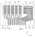
- FIG. 1 is a plan view showing a light emitting device 10 according to the embodiment.
- FIG. 2 is a view in which the covering layer 180 is removed from FIG.
- FIG. 3 is a view in which the partition 170 and the second conductive layer 230 are removed from FIG.
- FIG. 4 is a diagram in which the insulating layer 150 is removed from FIG.
- FIG. 5 is a cross-sectional view taken along the line AA in FIG. 6 is a cross-sectional view taken along the line BB in FIG. 7 is a cross-sectional view taken along the line CC of FIG.
- FIG. 8 is a sectional view taken along the line DD of FIG.
- the light emitting device 10 includes a substrate 100, a plurality of light emitting units 140, and an insulating layer 150.
- the plurality of light emitting units 140 are on the first surface 102 of the substrate 100.
- each light emitting unit 140 includes a first electrode 110, an organic layer 120, and a second electrode 130.
- the insulating layer 150 defines the light emitting unit 140.
- the light emitting unit 140 has a first side 142 and a second side 144.
- the first side 142 extends in the first direction (X direction in the drawing).
- the second side 144 extends in a direction intersecting the first side 142 (Y direction in the drawing).
- the insulating layer 150 has a first side surface 152a.
- the first side surface 152 a defines the first side 142 of the light emitting unit 140.
- the first side surface 152 a is inclined upward toward the outside of the light emitting unit 140 at an angle ⁇ 1 of 20 ° or less with respect to the first surface 102.
- the insulating layer 150 has a second side surface 154a.
- the second side surface 154 a defines the second side 144 of the light emitting unit 140.
- the second side surface 154 a is inclined upward toward the outside of the light emitting unit 140 at an angle ⁇ 2 of 20 ° or less with respect to the first surface 102.
- the insulating layer 150 is formed by ink jet printing. Accordingly, the inclination angle theta 2 of the inclination angle theta 1 and the second side surface 154a of the first side surface 152a are both turned 20 ° or less. Details will be described below.
- the light emitting device 10 is a display.
- the light emitting device 10 includes a substrate 100, a plurality of light emitting units 140, an insulating layer 150, a plurality of partition walls 170, a covering layer 180, a plurality of organic layers 220, a plurality of second conductive layers 230, a plurality of conductive layers 302, and a plurality of conductive layers. It has a layer 304.
- the substrate 100 has a first surface 102 and a second surface 104.
- the second surface 104 is on the opposite side of the first surface 102 and is the back surface of the substrate 100.
- the shape of the first surface 102 is a rectangle.
- the shape of the first surface 102 may be a polygon other than a rectangle, for example.
- the light emitting device 10 may be either bottom emission or top emission.
- the substrate 100 is made of a translucent material (for example, glass or resin).
- the light emitting device 10 is top emission, the light from the plurality of light emitting units 140 is emitted from above the first surface 102 of the substrate 100.
- the substrate 100 may be made of the above-described translucent material or may be made of a material that does not have translucency.
- the substrate 100 may have flexibility or may not have flexibility.
- the thickness of the substrate 100 is, for example, not less than 10 ⁇ m and not more than 1000 ⁇ m.
- the thickness of the substrate 100 is, for example, 200 ⁇ m or less.
- the substrate 100 is flexible and includes a resin
- the substrate 100 includes, for example, PEN (polyethylene naphthalate), PES (polyethersulfone), PET (polyethylene terephthalate), or polyimide.
- the first surface 102 (preferably both the first surface 102 and the second surface 104) of the substrate 100 may be covered with an inorganic barrier film (eg, SiN x or SiON). In this case, even if the substrate 100 includes a material (for example, resin) having a high water vapor transmission rate, the water vapor is prevented from reaching the first surface 102 of the substrate 100.
- an inorganic barrier film eg, SiN x or SiON
- each conductive layer 302 has a first terminal 112, a first wiring 114, and a first conductive layer 210.
- the first terminal 112 is one end of the conductive layer 302.
- the first conductive layer 210 is a part of the conductive layer 302.
- the first wiring 114 is a part of the conductive layer 302 and is between the first terminal 112 and the first conductive layer 210.
- Each conductive layer 304 has a second terminal 132 and a second wiring 134.
- the second terminal 132 is one end of the conductive layer 304.
- the second wiring 134 is a part of the conductive layer 304.
- a potential is applied to the first terminal 112.
- the potential of the first terminal 112 is applied to the first conductive layer 210 through the first wiring 114.
- a potential is applied to the second terminal 132.
- the potential of the second terminal 132 is applied to the second conductive layer 230 through the second wiring 134.
- the electric resistance of the conductive layer 190 is lower than the electric resistance of the conductive layer 302 and the electric resistance of the conductive layer 304. Thereby, a voltage drop between the first terminal 112 and the first conductive layer 210 and a voltage drop between the second terminal 132 and the second conductive layer 230 can be suppressed.
- the conductive layer 190 is positioned so as not to overlap the light emitting unit 140. For this reason, the conductive layer 190 does not need to have translucency.
- the conductive layer 190 is made of, for example, Al or Ag.
- the conductive layer 190 includes, for example, a Mo alloy layer on the top surface of the conductive layer 302 or the top surface of the conductive layer 304, an Al alloy layer on the Mo alloy layer, and a Mo alloy layer on the Al alloy layer. Also good.
- the plurality of first conductive layers 210 are arranged in the first direction (X direction in the figure). Each first conductive layer 210 extends in a second direction (Y direction in the drawing) that intersects the first direction (specifically, orthogonal to the first direction).
- the insulating layer 150 is on the first surface 102 of the substrate 100 and the plurality of first conductive layers 210.
- the insulating layer 150 includes an organic material (for example, polyimide).
- the insulating layer 150 has a plurality of openings 162.
- the plurality of openings 162 are arranged in a matrix.
- the shape of each opening 162 is a rectangle.
- a part of the first conductive layer 210 (first electrode 110) and a part of the second conductive layer 230 (second electrode 130) overlap each other. . Thereby, the region surrounded by the edge of the opening 162 functions as the light emitting unit 140.
- the insulating layer 150 defines the light emitting unit 140. 5, 6, 10, and 11, the light emitting unit 140 is formed on the side surface of the insulating layer 150 (the first side surface 152 a in the example illustrated in FIG. 10 and the second side surface in the example illustrated in FIG. 11). 154a) is defined by the lower end.
- the insulating layer 150 is formed by ink jet printing. For this reason, the inclination angle (for example, ⁇ 1 in FIG. 10 and ⁇ 2 in FIG. 11) of the insulating layer 150 with respect to the first surface 102 of the substrate 100 in the vicinity of the light emitting portion 140 becomes small, specifically 20 °. It becomes as follows. Thereby, the light emission characteristics of the light emitting unit 140 are uniform from the center to the edge of the light emitting unit 140.
- the film thickness of the organic layer 120 (organic layer 220) at the edge of the light emitting unit 140 and in the vicinity thereof is the center of the light emitting unit 140 and the vicinity thereof. Is substantially equal to the film thickness of the organic layer 120 (organic layer 220).
- the film thickness of the organic layer 120 (organic layer 220) at the edge of the light emitting unit 140 and the vicinity thereof is the center of the light emitting unit 140 and It is considerably thicker than the film thickness of the organic layer 120 (organic layer 220) in the vicinity thereof.
- Such a difference in film thickness may cause a difference between the light emission characteristics at the center of the light emitting unit 140 and its vicinity and the light emission characteristics at the edge of the light emitting unit 140 and its vicinity.
- there is almost no difference in film thickness in this embodiment, there is almost no difference in film thickness. For this reason, the light emission characteristics of the light emitting unit 140 are uniform from the center to the edge of the light emitting unit 140.
- the insulating layer 150 may contain fluorine, specifically, a fluorine-based surfactant.
- fluorine specifically, a fluorine-based surfactant.
- the fluorosurfactant contained in the ink when the insulating layer 150 is formed by inkjet printing remains in the insulating layer 150.
- the insulating layer 150 has water repellency, for example, a contact angle larger than 50 ° with respect to water.
- the surface of the insulating layer 150 may be covered with a film made of fluoride.
- the insulating layer 150 is treated with CF 4 plasma.
- the surface of the insulating layer 150 is covered with a film made of fluoride. This fluoride is derived from CF 4 in the CF 4 plasma. In this case, the surface of the insulating layer 150 has water repellency.
- the insulating layer 150 has a first portion 152, a second portion 154, and a third portion 156.
- the first portion 152 has an upper surface that intersects the first side surface 152a.
- the first portion 152 is adjacent to the first side 142 of the light emitting unit 140.
- the second portion 154 has an upper surface that intersects the second side surface 154a.
- the second portion 154 is adjacent to the second side 144 of the light emitting unit 140.
- the third portion 156 is outside the corner between the first side 142 and the second side 144.
- the third portion 156 is connected to the first portion 152 and the second portion 154.
- the film thickness of the insulating layer 150 is almost uniform in any region.
- the film thickness T3 of the third portion 156 is 95% or more and 105% or less of the film thickness T1 of the first portion 152, and is 95% or more and 105% or less of the film thickness T2 of the second portion 154. .
- the insulating layer 150 has an opening 164. As shown in FIG. 7, the second conductive layer 230 is connected to the second wiring 134 through the opening 164.
- each of the plurality of partition walls 170 is on the insulating layer 150.
- the partition 170 includes a photosensitive resin (for example, polyimide).
- the plurality of partition walls 170 are arranged in the second direction (Y direction in the figure).
- Each partition 170 extends in the first direction (X direction in the figure).
- the width of the upper surface of the partition wall 170 is wider than the width of the lower surface of the partition wall 170 in a cross section perpendicular to the first direction (the X direction in FIGS. 1 to 4). More specifically, in the cross section perpendicular to the first direction (the X direction in FIGS.
- the partition wall 170 has a first side surface and a second side surface.
- the second side surface is on the opposite side of the first inner surface.
- the first side surface of the partition wall 170 is inclined so that the upper end of the first side surface is located outside the lower end of the first side surface.
- the second side surface of the partition wall 170 is inclined so that the upper end of the second side surface is located outside the lower end of the second side surface.
- the plurality of organic layers 220 are on the first surface 102 of the substrate 100, on the plurality of first conductive layers 210, and on the insulating layer 150. As shown in FIG. 5, the plurality of organic layers 220 are arranged in the second direction (the Y direction in FIGS. 1 to 4). The organic layers 220 adjacent to each other face each other with the partition wall 170 interposed therebetween. As shown in FIGS. 5 and 6, part of the organic layer 220 overlaps with part of the first conductive layer 210 (first electrode 110). This part of the organic layer 220 functions as the organic layer 120 of the light emitting unit 140.
- the organic layer 220 is not in contact with the partition wall 170.
- a substance that degrades the organic layer 220 can be prevented from propagating from the partition wall 170 to the organic layer 220.
- the partition 170 may contain a substance (for example, water) that degrades the organic layer 220.
- this material may propagate from the organic layer 220 to the partition wall 170.
- the partition 170 includes the above-described substance, it is possible to prevent the substance from propagating to the organic layer 220.
- the organic layer 222 is on the upper surface of the partition wall 170.
- the material included in the organic layer 222 is the same as the material included in the organic layer 220.
- the organic layer 220 and the organic layer 222 are formed by depositing an organic layer on the first surface 102 and the partition wall 170 of the substrate 100. In this case, the organic layer is separated into the organic layer 220 and the organic layer 222 by the partition 170.
- the organic layer 220 has, for example, a hole injection layer, a hole transport layer, a light emitting layer, an electron transport layer, and an electron injection layer.
- the total thickness of the organic layer 220 is, for example, not less than 50 nm and not more than 200 nm. Holes move in the hole injection layer and the hole transport layer.
- the thickness of the hole injection layer is, for example, not less than 50 nm and not more than 100 nm.
- the thickness of the hole transport layer is thinner than the thickness of the hole injection layer.
- the thickness of the hole transport layer is, for example, 20 nm or more and 50 nm or less.
- the color of light from the light emitting layer is, for example, red, green, or blue.
- electrons are transported.
- the thickness of the electron transport layer is, for example, 5 nm or more and 100 nm or less.
- the electron injection layer is made of an alkali metal compound (for example, LiF), a metal oxide (for example, aluminum oxide) or a metal complex (for example, lithium 8-hydroxyquinolate (Liq)).
- the thickness of the electron injection layer is, for example, not less than 0.1 nm and not more than 10 nm.
- One of the hole injection layer and the hole transport layer may be omitted.
- One of the electron transport layer and the electron injection layer may be omitted.
- the hole injection layer, hole transport layer, light emitting layer, electron transport layer, and electron injection layer are formed by, for example, a coating process. Specifically, for example, the hole injection layer, the hole transport layer, and the light emitting layer are formed by a coating process.
- the electron transport layer and the electron injection layer are formed by vapor deposition.
- each of the plurality of second conductive layers 230 is on the organic layer 220. As shown in FIG. 2, the plurality of second conductive layers 230 are arranged in the second direction (Y direction in the figure). Each second conductive layer 230 extends in the first direction (X direction in the figure). The second conductive layers 230 adjacent to each other face each other across the partition wall 170. As shown in FIGS. 5 and 6, a part of the second conductive layer 230 overlaps a part of the first conductive layer 210 (first electrode 110). This part of the second conductive layer 230 functions as the second electrode 130 of the light emitting unit 140.
- the second conductive layer 232 is on the upper surface of the partition wall 170.
- the material included in the second conductive layer 232 is the same as the material included in the second conductive layer 230.
- the second conductive layer 230 and the second conductive layer 232 are formed by depositing a conductive layer on the first surface 102 and the partition wall 170 of the substrate 100. In this case, the conductive layer is separated into the second conductive layer 230 and the second conductive layer 232 by the partition 170.
- the first conductive layer 210 is a conductive layer having translucency. In this case, the second conductive layer 230 does not need to have translucency.
- the second conductive layer 230 is a conductive layer having translucency. In this case, the first conductive layer 210 does not need to have translucency.
- the first conductive layer 210 and the second conductive layer 230 are light-transmitting conductive layers
- the first conductive layer 210 and the second conductive layer 230 include, for example, a metal oxide, and more specifically, for example, It contains ITO (Indium Tin Oxide), IZO (Indium Zinc Oxide), IWZO (Indium Tungsten Zinc Oxide) or ZnO (Zinc Oxide).
- the first conductive layer 210 and the second conductive layer 230 are non-translucent conductive layers
- the first conductive layer 210 and the second conductive layer 230 include, for example, Al, Au, Ag, Pt, Mg, Sn, A metal selected from the first group consisting of Zn and In or an alloy of a metal selected from the first group is included.
- the covering layer 180 covers the insulating layer 150, the plurality of light emitting portions 140, and the plurality of partition walls 170. Thereby, the coating layer 180 seals the insulating layer 150, the plurality of light emitting units 140, and the plurality of partition walls 170.
- the covering layer 200 includes, for example, an insulating material, more specifically, for example, a metal oxide.
- the covering layer 180 includes, for example, a titanium oxide layer and an aluminum oxide layer. In this case, the aluminum oxide layer is on the titanium oxide layer or below the titanium oxide layer.
- the thickness of the coating layer 200 is, for example, not less than 50 nm and not more than 300 nm.
- the covering layer 180 is formed by, for example, ALD (Atomic Layer Deposition).
- the covering layer 180 may be formed by, for example, CVD (Chemical Vapor Deposition) or sputtering.
- the covering layer 180 includes, for example, a SiO 2 layer or a SiN layer.
- the film thickness of the coating layer 180 is, for example, not less than 10 nm and not more than 1000 nm.
- the covering layer 180 may be covered with a resin layer.
- the resin layer is provided to protect the covering layer 180.
- the resin layer contains, for example, an epoxy resin or an acrylic resin.
- a method for manufacturing the light emitting device 10 will be described.
- a conductive layer is formed on the first surface 102 of the substrate 100, and this conductive layer is patterned. Thereby, a plurality of conductive layers 302 (first terminal 112, first wiring 114 and first conductive layer 210) and a plurality of conductive layers 304 (second terminal 132 and second wiring 134) are formed.
- a conductive layer 190 is formed over the top surface of each conductive layer 302 and the top surface of each conductive layer 304.
- the insulating layer 150 is formed on the first surface 102 of the substrate 100, the plurality of conductive layers 302, and the plurality of conductive layers 304.
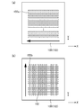
- FIG. 13 is a flowchart for explaining a method of forming the insulating layer 150 shown in FIGS.
- FIG. 14 is a diagram for explaining a method of forming the insulating layer 150 shown in FIGS.
- the first ink 150a is applied along the first direction (X direction in the figure) (step S10).
- the first ink 150a includes a material (for example, polyimide and a fluorine-based surfactant) included in the insulating layer 150.
- the first ink 150a is arranged such that the area where the first ink 150a is applied and the area where the first ink 150a is not applied are alternately arranged along the second direction (Y direction in the figure). It is applied along the first direction (X direction in the figure).
- the plurality of first inks 150a arranged in the second direction (Y direction in the figure) are applied simultaneously.
- the second ink 150b is applied along the second direction (the Y direction in the figure) (step S20).
- the second ink 150b includes a material (for example, polyimide and a fluorine-based surfactant) included in the insulating layer 150.
- the second ink 150b is configured such that the region where the second ink 150b is applied and the region where the second ink 150b is not applied are alternately arranged along the first direction (X direction in the drawing). It is applied along the second direction (Y direction in the figure).
- the second ink 150b is applied so as to intersect the first ink 150a. Thereby, the opening 162 is formed.
- a plurality of second inks 150b arranged in the first direction (X direction in the drawing) are applied simultaneously.
- step S20 is performed before the first ink 150a is dried. Specifically, the step of applying the second ink 150b (step S20) is started within, for example, 5 minutes after the step of applying the first ink 150a (step S10) is completed. Thereby, the film thickness of the insulating layer 150 becomes substantially uniform in any region.
- step S30 the first ink 150a and the second ink 150b are dried (step S30). Specifically, as an example of step S30, the first ink 150a and the second ink 150b are dried in a vacuum environment. As another example of step S30, the first ink 150a and the second ink 150b may be baked at 100 ° C. for 3 minutes. Next, the resin in the first ink 150a and the second ink 150b is cured by heating. In this way, the insulating layer 150 is formed.
- the third portion 156 of the insulating layer 150 is located at the intersection of the first ink 150a and the second ink 150b.
- the first portion 152 is located in a region where the first ink 150a is applied.
- the second portion 154 is located in a region where the second ink 150b is applied.
- the plurality of third portions 156 includes m rows (m is an integer of 2 or more) along the first direction (X direction in the drawing) and the second direction (Y direction in the drawing). Are arranged in a matrix including n columns (where n is an integer of 2 or more).
- the third portions 156 adjacent to each other in the first direction (X direction in the drawing) are connected to each other via the first portion 152.
- Third portions 156 adjacent to each other in the second direction (Y direction in the drawing) are connected to each other via the second portion 154.
- a plurality of partition walls 170 are formed on the insulating layer 150.
- an organic layer is formed on the insulating layer 150 and the plurality of partition walls 170. Accordingly, the organic layer is separated into the organic layer 220 and the organic layer 222 by the partition wall 170.
- a conductive layer is formed over the insulating layer 150 and the plurality of partition walls 170. Accordingly, the conductive layer is separated into the second conductive layer 230 and the second conductive layer 232 by the partition wall 170.
- a coating layer 180 is formed by ALD on the first surface 102 of the substrate 100, the insulating layer 150, and the plurality of partition walls 170.
- the insulating layer 150, the plurality of light emitting units 140, and the plurality of partition walls 170 are sealed by the covering layer 180.
- the insulating layer 150 is formed by inkjet printing. Specifically, the first ink 150a is applied, and the second ink 150b is applied so as to intersect the first ink 150a. The first ink 150a is not dried between the application of the first ink 150a and the application of the second ink 150b. Thereby, the film thickness of the insulating layer 150 becomes substantially uniform in any region.
- FIG. 15A is a diagram showing an optical microscope image of the insulating layer 150 according to the example.
- FIG. 15B is an enlarged view of a part of FIG.
- FIG. 15C is a diagram showing an interference microscope image of the insulating layer 150 shown in FIG. In this example, the insulating layer 150 was formed by the method shown in FIGS.
- FIG. 16A is a diagram showing an optical microscope image of the insulating layer 150 according to Comparative Example 1.
- FIG. 16B is an enlarged view of a part of FIG.
- FIG. 16C shows an interference microscope image of the insulating layer 150 shown in FIG.
- the first ink 150a was heated at 80 ° C. for 5 minutes between the step of applying the first ink 150a (step S10) and the step of applying the second ink 150b (step S20).
- FIG. 17A is a diagram showing an optical microscope image of the insulating layer 150 according to Comparative Example 2.
- FIG. 17B is an enlarged view of a part of FIG.
- FIG. 17C is a diagram showing an interference microscope image of the insulating layer 150 shown in FIG.
- the first ink 150a was heated at 80 ° C. for 5 minutes between the step of applying the first ink 150a (step S10) and the step of applying the second ink 150b (step S20). Thereafter, the first ink 150a was heated at 300 ° C. for 1 hour before the step of applying the second ink 150b (step S20).
- the film thickness of the insulating layer 150 was almost constant in any region.
- the thickness of the insulating layer 150 is the portion where the first ink 150a and the second ink 150b intersect (the third portion shown in FIG. 9). 156), which was significantly thicker than the other regions.
- the opening 162 was not formed.
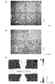
- FIG. 18A is a view showing an electron microscope image of a cross section of the insulating layer 150 formed by the method shown in FIGS.
- FIG. 18B is a height profile of the insulating layer 150 shown in FIG.
- the inclination angle of the insulating layer 150 was less than 5 °.
- the inclination angle of the insulating layer 150 formed by the method shown in FIGS. 13 and 14 is small.
Landscapes
- Engineering & Computer Science (AREA)
- Manufacturing & Machinery (AREA)
- Electroluminescent Light Sources (AREA)
Abstract
第1方向(図中、X方向)に沿って第1インク(150a)を塗布する。第1インク(150a)は、第1インク(150a)が塗布された領域と第1インク(150a)が塗布されない領域が第2方向(図中、Y方向)に沿って交互に並ぶように第1方向(図中、X方向)に沿って塗布される。第2方向(図中、Y方向)に沿って第2インク(150b)を塗布する。第2インク(150b)は、第2インク(150b)が塗布された領域と第2インク(150b)が塗布されない領域が第1方向(図中、X方向)に沿って交互に並ぶように第2方向(図中、Y方向)に沿って塗布される。第2インク(150b)は、第1インク(150a)が乾燥する前に塗布される。
Description
本発明は、発光装置の製造方法及び発光装置に関する。
発光装置では、発光部を画定するための絶縁層が形成されることがある。特許文献1には、このような絶縁層をフォトリソグラフィにより形成することが記載されている。
本発明者は、発光部を画定するための絶縁層を形成するための新規な方法を検討した。
本発明が解決しようとする課題としては、発光部を画定するための絶縁層を新規な方法により形成することが一例として挙げられる。
請求項1に記載の発明は、
発光部及び前記発光部を画定する絶縁層を備える発光装置の製造方法であって、
前記絶縁層をインクジェット印刷により形成する工程を含む、発光装置の製造方法である。
発光部及び前記発光部を画定する絶縁層を備える発光装置の製造方法であって、
前記絶縁層をインクジェット印刷により形成する工程を含む、発光装置の製造方法である。
請求項6に記載の発明は、
第1面を有する基板と、
前記第1面上にあり、有機層を有し、第1辺及び前記第1辺に交差する方向に延伸する第2辺を有する発光部と、
前記第1辺を画定する第1側面及び前記第2辺を画定する第2側面を有する絶縁層と、
を備え、
前記第1側面は、前記第1面に対して20°以下の角度で前記発光部の外側に向けて上方に傾斜しており、
前記第2側面は、前記第1面に対して20°以下の角度で前記発光部の外側に向けて上方に傾斜している発光装置である。
第1面を有する基板と、
前記第1面上にあり、有機層を有し、第1辺及び前記第1辺に交差する方向に延伸する第2辺を有する発光部と、
前記第1辺を画定する第1側面及び前記第2辺を画定する第2側面を有する絶縁層と、
を備え、
前記第1側面は、前記第1面に対して20°以下の角度で前記発光部の外側に向けて上方に傾斜しており、
前記第2側面は、前記第1面に対して20°以下の角度で前記発光部の外側に向けて上方に傾斜している発光装置である。
上述した目的、およびその他の目的、特徴および利点は、以下に述べる好適な実施の形態、およびそれに付随する以下の図面によってさらに明らかになる。
以下、本発明の実施の形態について、図面を用いて説明する。尚、すべての図面において、同様な構成要素には同様の符号を付し、適宜説明を省略する。
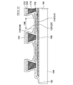
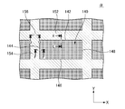
図1は、実施形態に係る発光装置10を示す平面図である。図2は、図1から被覆層180を取り除いた図である。図3は、図2から隔壁170及び第2導電層230を取り除いた図である。図4は、図3から絶縁層150を取り除いた図である。図5は、図2のA-A断面図である。図6は、図2のB-B断面図である。図7は、図2のC-C断面図である。図8は、図2のD-D断面図である。図9は、図3に示したαを拡大した図である。図10は、図9のE-E断面図である。図11は、図9のF-F断面図である。図12は、図9のG-G断面図である。
発光装置10は、基板100、複数の発光部140及び絶縁層150を備えている。複数の発光部140は、基板100の第1面102上にある。図5及び図6に示すように、各発光部140は、第1電極110、有機層120及び第2電極130を有している。絶縁層150は、発光部140を画定している。具体的には、図9に示すように、発光部140は、第1辺142及び第2辺144を有している。第1辺142は、第1方向(図中、X方向)に延伸している。第2辺144は、第1辺142に交差する方向(図中、Y方向)に延伸している。図10に示すように、絶縁層150は、第1側面152aを有している。第1側面152aは、発光部140の第1辺142を画定している。第1側面152aは、第1面102に対して20°以下の角度θ1で発光部140の外側に向けて上方に傾斜している。図11に示すように、絶縁層150は、第2側面154aを有している。第2側面154aは、発光部140の第2辺144を画定している。第2側面154aは、第1面102に対して20°以下の角度θ2で発光部140の外側に向けて上方に傾斜している。後述する図13及び図14を用いて説明するように、絶縁層150は、インクジェット印刷により形成される。これにより、第1側面152aの傾斜角θ1及び第2側面154aの傾斜角θ2は、いずれも20°以下になっている。以下、詳細に説明する。
図1~図9に示す例において、発光装置10は、ディスプレイである。発光装置10は、基板100、複数の発光部140、絶縁層150、複数の隔壁170、被覆層180、複数の有機層220、複数の第2導電層230、複数の導電層302及び複数の導電層304を有している。
図5~図8に示すように、基板100は、第1面102及び第2面104を有している。第2面104は、第1面102の反対側にあり、基板100の裏面である。図1~図4に示す例では、第1面102の形状は、矩形である。ただし、第1面102の形状は、例えば矩形以外の多角形であってもよい。
発光装置10は、ボトムエミッション及びトップエミッションのいずれであってもよい。発光装置10がボトムエミッションである場合、複数の発光部140からの光は、基板100の第2面104から出射される。この場合、基板100は、透光性の材料(例えばガラス又は樹脂)からなる。これに対して、発光装置10がトップエミッションである場合、複数の発光部140からの光は、基板100の第1面102の上方から出射される。この場合、基板100は、上記した透光性の材料からなってもよいし、又は透光性を有しない材料からなってもよい。
基板100は、可撓性を有していてもよいし、又は可撓性を有していなくてもよい。基板100が可撓性を有する場合、基板100の厚さは、例えば10μm以上1000μm以下である。基板100が可撓性を有し、かつガラスを含む場合、基板100の厚さは、例えば200μm以下である。基板100が可撓性を有し、かつ樹脂を含む場合、基板100は、例えばPEN(ポリエチレンナフタレート)、PES(ポリエーテルサルホン)、PET(ポリエチレンテレフタラート)又はポリイミドを含む。なお、基板100の第1面102(好ましくは、第1面102及び第2面104の双方)は、無機バリア膜(例えばSiNx又はSiON)により覆われていてもよい。この場合、基板100が水蒸気透過率の高い材料(例えば樹脂)を含んでいても、水蒸気が基板100の第1面102よりも上に達することが抑制される。
図4に示すように、各導電層302は、第1端子112、第1配線114及び第1導電層210を有している。第1端子112は、導電層302の一端である。第1導電層210は、導電層302の一部である。第1配線114は、導電層302の一部であり、第1端子112と第1導電層210の間にある。各導電層304は、第2端子132及び第2配線134を有している。第2端子132は、導電層304の一端である。第2配線134は、導電層304の一部である。第1端子112には、電位が与えられる。これにより、第1端子112の電位は、第1配線114を介して第1導電層210に与えられる。第2端子132には、電位が与えられる。これにより、第2端子132の電位は、第2配線134を介して第2導電層230に与えられる。
導電層302上及び導電層304上の各々には、導電層190がある。導電層190の電気抵抗は、導電層302の電気抵抗及び導電層304の電気抵抗よりも低い。これにより、第1端子112と第1導電層210の間の電圧降下及び第2端子132と第2導電層230の間の電圧降下を抑制することができる。導電層190は、発光部140と重ならないように位置している。このため、導電層190は、透光性を有する必要がない。具体的には、導電層190は、例えばAl又はAgからなる。その他の例として、導電層190は、例えば導電層302の上面上又は導電層304の上面上のMo合金層、Mo合金層上のAl合金層及びAl合金層上のMo合金層を含んでいてもよい。
図4に示すように、複数の第1導電層210は、第1方向(図中、X方向)に並んでいる。各第1導電層210は、第1方向に交わる(具体的には、第1方向に直交する)第2方向(図中、Y方向)に延伸している。
図5、図7及び図8に示すように、絶縁層150は、基板100の第1面102上及び複数の第1導電層210上にある。絶縁層150は、有機材料(例えばポリイミド)を含んでいる。図3に示すように、絶縁層150は、複数の開口162を有する。複数の開口162は、行列状に並んでいる。各開口162の形状は、矩形である。図5及び図6に示すように、各開口162内では、第1導電層210の一部(第1電極110)と第2導電層230の一部(第2電極130)が互いに重なっている。これにより、開口162の縁によって囲まれた領域が発光部140として機能する。すなわち、絶縁層150は、発光部140を画定している。なお、図5、図6、図10及び図11に示すように、発光部140は、絶縁層150の側面(図10に示す例では第1側面152a及び図11に示す例では、第2側面154a)の下端によって画定されている。
後述する図13及び図14を用いて説明するように、絶縁層150は、インクジェット印刷により形成される。このため、発光部140の近傍において基板100の第1面102に対する絶縁層150の傾斜角(例えば、図10のθ1及び図11のθ2)は、小さいものとなり、具体的には20°以下となる。これにより、発光部140の中央から縁に亘って発光部140の発光特性が均一になる。
詳細には、本実施形態においては、例えば図10及び図11に示すように、発光部140の縁及びその近傍における有機層120(有機層220)の膜厚が発光部140の中央及びその近傍における有機層120(有機層220)の膜厚とほぼ等しい。これに対して、仮に、上記した傾斜角が大きく、例えば90°程度であった場合、発光部140の縁及びその近傍における有機層120(有機層220)の膜厚が発光部140の中央及びその近傍における有機層120(有機層220)の膜厚よりも相当に厚くなる。このような膜厚の差は、発光部140の中央及びその近傍における発光特性と発光部140の縁及びその近傍における発光特性の差の原因になり得る。これに対して本実施形態では、このような膜厚の差がほとんどない。このため、発光部140の中央から縁に亘って発光部140の発光特性が均一になる。
絶縁層150は、フッ素、具体的にはフッ素系界面活性剤を含んでいてもよい。言い換えると、絶縁層150をインクジェット印刷により形成する際のインクに含有されているフッ素系界面活性剤が絶縁層150に残留している。この場合、絶縁層150は、撥水性を有し、例えば水に対して50°よりも大きい接触角を有する。なお、絶縁層150の表面は、フッ化物からなる膜により覆われていてもよい。具体的には、絶縁層150をインクジェット印刷により形成した後(このインクジェット印刷では、親水性のインクを用いてもよい。)、絶縁層150をCF4プラズマで処理する。これにより、絶縁層150の表面は、フッ化物からなる膜により覆われる。このフッ化物は、CF4プラズマ中のCF4に由来する。この場合、絶縁層150の表面は、撥水性を有するようになる。
図9に示すように、絶縁層150は、第1部分152、第2部分154及び第3部分156を有している。図10に示すように、第1部分152は、第1側面152aに交わる上面を有している。第1部分152は、発光部140の第1辺142に隣接している。図11に示すように、第2部分154は、第2側面154aに交わる上面を有している。第2部分154は、発光部140の第2辺144に隣接している。図9及び図12に示すように、第3部分156は、第1辺142と第2辺144の間の角の外側にある。第3部分156は、第1部分152及び第2部分154に接続している。
後述する図13及び図14を用いて説明するように、本実施形態に係るインクジェット印刷では、絶縁層150の膜厚がいずれの領域においてもほぼ均一になる。具体的には、第3部分156の膜厚T3は、第1部分152の膜厚T1の95%以上105%以下であり、第2部分154の膜厚T2の95%以上105%以下である。
絶縁層150は、開口164を有する。図7に示すように、第2導電層230は、開口164を介して第2配線134に接続している。
図5、図7及び図8に示すように、複数の隔壁170の各々は、絶縁層150上にある。隔壁170は、感光性樹脂(例えばポリイミド)を含んでいる。図2に示すように、複数の隔壁170は、第2方向(図中、Y方向)に並んでいる。各隔壁170は、第1方向(図中、X方向)に延伸している。図5及び図7に示すように、第1方向(図1~図4のX方向)に垂直な断面において、隔壁170の上面の幅は、隔壁170の下面の幅よりも広い。より詳細には、第1方向(図1~図4のX方向)に垂直な断面において、隔壁170は、第1側面及び第2側面を有している。第2側面は、第1内側面の反対側にある。隔壁170の第1側面は、第1側面の上端が第1側面の下端よりも外側に位置するように傾いている。隔壁170の第2側面は、第2側面の上端が第2側面の下端よりも外側に位置するように傾いている。
図5及び図6に示すように、複数の有機層220は、基板100の第1面102上、複数の第1導電層210上及び絶縁層150上にある。図5に示すように、複数の有機層220は、第2方向(図1~図4のY方向)に並んでいる。互いに隣接する有機層220は、隔壁170を挟んで互いに対向している。図5及び図6に示すように、有機層220の一部は、第1導電層210の一部(第1電極110)と重なっている。有機層220のこの一部は、発光部140の有機層120として機能する。
なお、図5及び図7に示すように、有機層220は、隔壁170とは接していない。この場合、有機層220を劣化させる物質が隔壁170から有機層220に伝搬することを抑制することができる。詳細には、隔壁170は、有機層220を劣化させる物質(例えば、水)を含んでいることがある。この場合、有機層220が隔壁170と接していると、この物質が有機層220から隔壁170に伝搬することがある。これに対して図5及び図7に示す例では、隔壁170が上記した物質を含んでいたとしても、この物質が有機層220に伝搬することを抑制することができる。
図5及び図8に示すように、隔壁170の上面上には、有機層222がある。有機層222に含まれる材料は、有機層220に含まれる材料と同一である。有機層220及び有機層222は、基板100の第1面102上及び隔壁170上に有機層を堆積することにより形成される。この場合、有機層は、隔壁170によって有機層220と有機層222に分離される。
有機層220は、例えば正孔注入層、正孔輸送層、発光層、電子輸送層及び電子注入層を有している。有機層220全体の厚さは、例えば50nm以上200nm以下である。正孔注入層内及び正孔輸送層内では、正孔が移動する。正孔注入層の厚さは、例えば50nm以上100nm以下である。正孔輸送層の厚さは、正孔注入層の厚さよりも薄い。正孔輸送層の厚さは、例えば20nm以上50nm以下である。発光層では、電子と正孔が再結合する。これにより、発光層からは、光が発せられる。発光層からの光の色は、例えば赤、緑又は青である。電子輸送層では、電子が輸送される。電子輸送層の厚さは、例えば5nm以上100nm以下である。電子注入層は、アルカリ金属化合物(例えばLiF)、金属酸化物(例えば酸化アルミニウム)又は金属錯体(例えばリチウム8-ヒドロキシキノレート(Liq))からなる。電子注入層の厚さは、例えば0.1nm以上10nm以下である。
なお、正孔注入層及び正孔輸送層の一方はなくてもよい。電子輸送層及び電子注入層の一方はなくてもよい。
正孔注入層、正孔輸送層、発光層、電子輸送層及び電子注入層は、例えば塗布プロセスにより形成される。具体的には、例えば正孔注入層、正孔輸送層及び発光層は、塗布プロセスにより形成され。電子輸送層及び電子注入層は、蒸着により形成される。
図5及び図6に示すように、複数の第2導電層230の各々は、有機層220上にある。図2に示すように、複数の第2導電層230は、第2方向(図中、Y方向)に並んでいる。各第2導電層230は、第1方向(図中、X方向)に延伸している。互いに隣接する第2導電層230は、隔壁170を挟んで互いに対向している。図5及び図6に示すように、第2導電層230の一部は、第1導電層210の一部(第1電極110)と重なっている。第2導電層230のこの一部は、発光部140の第2電極130として機能する。
図5、図7及び図8に示すように、隔壁170の上面上には、第2導電層232がある。第2導電層232に含まれる材料は、第2導電層230に含まれる材料と同一である。第2導電層230及び第2導電層232は、基板100の第1面102上及び隔壁170上に導電層を堆積することにより形成される。この場合、導電層は、隔壁170によって第2導電層230と第2導電層232に分離される。
発光装置10がボトムエミッションである場合、第1導電層210は、透光性を有する導電層である。この場合、第2導電層230は、透光性を有する必要はない。これに対して、発光装置10がトップエミッションである場合、第2導電層230は、透光性を有する導電層である。この場合、第1導電層210は、透光性を有する必要はない。
第1導電層210及び第2導電層230が透光性を有する導電層である場合、第1導電層210及び第2導電層230は、例えば金属酸化物を含み、より具体的には、例えばITO(Indium Tin Oxide)、IZO(Indium Zinc Oxide)、IWZO(Indium Tungsten Zinc Oxide)又はZnO(Zinc Oxide)を含んでいる。
第1導電層210及び第2導電層230が透光性を有しない導電層である場合、第1導電層210及び第2導電層230は、例えばAl、Au、Ag、Pt、Mg、Sn、Zn及びInからなる第1群の中から選択される金属又はこの第1群から選択される金属の合金を含んでいる。
図5~図8に示すように、被覆層180は、絶縁層150、複数の発光部140及び複数の隔壁170を覆っている。これにより、被覆層180は、絶縁層150、複数の発光部140及び複数の隔壁170を封止している。被覆層200は、例えば絶縁材料、より具体的には例えば金属酸化物を含んでいる。被覆層180は、例えば酸化チタン層及び酸化アルミニウム層を含んでいる。この場合、酸化アルミニウム層は、酸化チタン層上又は酸化チタン層下にある。被覆層200の厚さは、例えば50nm以上300nm以下である。被覆層180は、例えばALD(Atomic Layer Deposition)によって形成されている。
なお、被覆層180は、例えばCVD(Chemical Vapor Deposition)又はスパッタにより形成してもよい。この場合、被覆層180は、例えばSiO2層又はSiN層を含んでいる。この場合、被覆層180の膜厚は、例えば10nm以上1000nm以下である。
被覆層180は、樹脂層により覆われていてもよい。樹脂層は、被覆層180を保護するために設けられている。樹脂層は、例えばエポキシ樹脂又はアクリル樹脂を含んでいる。
次に、発光装置10の製造方法について説明する。まず、基板100の第1面102上に導電層を形成し、この導電層をパターニングする。これにより、複数の導電層302(第1端子112、第1配線114及び第1導電層210)及び複数の導電層304(第2端子132及び第2配線134)が形成される。次いで、各導電層302の上面上及び各導電層304の上面上に導電層190を形成する。
次いで、基板100の第1面102上、複数の導電層302上及び複数の導電層304上に絶縁層150を形成する。
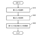
図13は、図1~図12に示した絶縁層150を形成する方法を説明するためのフローチャートである。図14は、図1~図12に示した絶縁層150を形成する方法を説明するための図である。
まず、図14(a)に示すように、第1方向(図中、X方向)に沿って第1インク150aを塗布する(ステップS10)。第1インク150aは、絶縁層150に含まれる材料(例えば、ポリイミド及びフッ素系界面活性剤)を含んでいる。本図に示す例では、第1インク150aは、第1インク150aが塗布された領域と第1インク150aが塗布されない領域が第2方向(図中、Y方向)に沿って交互に並ぶように第1方向(図中、X方向)に沿って塗布される。なお、第2方向(図中、Y方向)に並ぶ複数の第1インク150aは、同時に塗布される。
次いで、図14(b)に示すように、第2方向(図中、Y方向)に沿って第2インク150bを塗布する(ステップS20)。第2インク150bは、絶縁層150に含まれる材料(例えば、ポリイミド及びフッ素系界面活性剤)を含んでいる。本図に示す例では、第2インク150bは、第2インク150bが塗布された領域と第2インク150bが塗布されない領域が第1方向(図中、X方向)に沿って交互に並ぶように第2方向(図中、Y方向)に沿って塗布される。第2インク150bは、第1インク150aと交差するように塗布される。これにより、開口162が形成される。なお、第1方向(図中、X方向)に並ぶ複数の第2インク150bは、同時に塗布される。
なお、第2インク150bを塗布する工程(ステップS20)は、第1インク150aが乾燥する前に実施する。具体的には、第1インク150aを塗布する工程(ステップS10)が終了してから例えば5分以内に第2インク150bを塗布する工程(ステップS20)を開始する。これにより、絶縁層150の膜厚がいずれの領域においてもほぼ均一になる。
次いで、第1インク150a及び第2インク150bを乾燥させる(ステップS30)。具体的には、ステップS30の一例として、第1インク150a及び第2インク150bを真空環境内で乾燥させる。ステップS30のその他の例として、第1インク150a及び第2インク150bを100℃で3分間焼成してもよい。次いで、加熱により第1インク150a及び第2インク150b中の樹脂を硬化させる。このようにして、絶縁層150が形成される。
図9及び図14に示すように、絶縁層150の第3部分156は、第1インク150aと第2インク150bの交点に位置する。第1部分152は、第1インク150aが塗布された領域に位置する。第2部分154は、第2インク150bが塗布された領域に位置する。これにより、複数の第3部分156は、第1方向(図中、X方向)に沿ったm個(mは2以上の整数である。)の行及び第2方向(図中、Y方向)に沿ったn個(nは2以上の整数である。)の列を含む行列状に並ぶ。この場合、第1方向(図中、X方向)に互いに隣接する第3部分156は、第1部分152を介して互いに接続する。第2方向(図中、Y方向)に互いに隣接する第3部分156は、第2部分154を介して互いに接続する。
次いで、絶縁層150上に複数の隔壁170を形成する。
次いで、絶縁層150上及び複数の隔壁170上に有機層を形成する。これにより、有機層は、隔壁170によって有機層220及び有機層222に分離される。
次いで、絶縁層150上及び複数の隔壁170上に導電層を形成する。これにより、導電層は、隔壁170によって第2導電層230及び第2導電層232に分離される。
次いで、基板100の第1面102上、絶縁層150上及び複数の隔壁170上に被覆層180をALDにより形成する。これにより、絶縁層150、複数の発光部140及び複数の隔壁170は、被覆層180によって封止される。
以上、本実施形態によれば、絶縁層150は、インクジェット印刷により形成される。具体的には、第1インク150aを塗布し、第2インク150bを第1インク150aと交差するように塗布する。第1インク150aを塗布してから第2インク150bを塗布するまでの間に第1インク150aを乾燥させない。これにより、絶縁層150の膜厚は、いずれの領域においてもほぼ均一になる。
図15(a)は、実施例に係る絶縁層150の光学顕微鏡像を示す図である。図15(b)は、図15(a)の一部を拡大した図である。図15(c)は、図15(a)に示した絶縁層150の干渉顕微鏡像を示す図である。本実施例では、図13及び図14に示した方法で絶縁層150を形成した。
図16(a)は、比較例1に係る絶縁層150の光学顕微鏡像を示す図である。図16(b)は、図16(a)の一部を拡大した図である。図16(c)は、図16(a)に示した絶縁層150の干渉顕微鏡像を示す図である。本比較例では、第1インク150aを塗布する工程(ステップS10)と第2インク150bを塗布する工程(ステップS20)の間で第1インク150aを5分間80℃で加熱した。
図17(a)は、比較例2に係る絶縁層150の光学顕微鏡像を示す図である。図17(b)は、図17(a)の一部を拡大した図である。図17(c)は、図17(a)に示した絶縁層150の干渉顕微鏡像を示す図である。本比較例では、第1インク150aを塗布する工程(ステップS10)と第2インク150bを塗布する工程(ステップS20)の間で第1インク150aを5分間80℃で加熱した。その後、第2インク150bを塗布する工程(ステップS20)前に第1インク150aを1時間300℃で加熱した。
図15(c)に示すように、本実施例では、絶縁層150の膜厚は、いずれの領域においてもほぼ一定となった。これに対して、図16(c)に示すように、比較例1では、絶縁層150の膜厚は、第1インク150aと第2インク150bが交差する部分(図9に示した第3部分156に相当)において、その他の領域よりも有意に厚くなった。図17(a)~図17(c)に示すように、比較例2では、開口162が形成されなかった。これらの結果は、絶縁層150の膜厚がいずれの領域でもほぼ均一になる理由が、第1インク150aを塗布する工程(ステップS10)と第2インク150bを塗布する工程(ステップS20)の間で第1インク150aを乾燥させていないことに起因することを示唆している。
図18(a)は、図13及び図14に示した方法で形成した絶縁層150の断面の電子顕微鏡像を示す図である。図18(b)は、図18(a)に示した絶縁層150の高さプロファイルである。本図に示すように、絶縁層150の傾斜角は、5°未満となった。このように、図13及び14に示した方法で形成した絶縁層150の傾斜角は、小さいものとなった。
以上、図面を参照して実施形態及び実施例について述べたが、これらは本発明の例示であり、上記以外の様々な構成を採用することもできる。
Claims (9)
- 発光部及び前記発光部を画定する絶縁層を備える発光装置の製造方法であって、
前記絶縁層をインクジェット印刷により形成する工程を含む、発光装置の製造方法。 - 請求項1に記載の発光装置の製造方法において、
前記絶縁層を形成する工程は、
第1方向に沿って第1インクを塗布する工程と、
前記第1インクを塗布した後、前記第1方向とは異なる第2方向に沿って第2インクを塗布する工程と、
を含む、発光装置の製造方法。 - 請求項2に記載の発光装置の製造方法において、
前記第2インクを塗布する工程では、前記第2インクは前記第1インクと交差するように塗布される、発光装置の製造方法。 - 請求項2又は3に記載の発光装置の製造方法において、
前記第1インクを塗布する工程において、前記第1インクは、前記第1インクが塗布された領域と前記第1インクが塗布されていない領域が前記第2方向に沿って交互に並ぶように前記第1方向に沿って塗布され、
前記第2インクを塗布する工程において、前記第2インクは、前記第2インクが塗布された領域と前記第2インクが塗布されていない領域が前記第1方向に沿って交互に並ぶように前記第2方向に沿って塗布される、発光装置の製造方法。 - 請求項2~4のいずれか一項に記載の発光装置の製造方法において、
前記第1インク及び前記第2インクの塗布後、前記第1インク及び前記第2インクを乾燥させる工程を含む、発光装置の製造方法。 - 第1面を有する基板と、
前記第1面上にあり、有機層を有し、第1辺及び前記第1辺に交差する方向に延伸する第2辺を有する発光部と、
前記第1辺を画定する第1側面及び前記第2辺を画定する第2側面を有する絶縁層と、
を備え、
前記第1側面は、前記第1面に対して20°以下の角度で前記発光部の外側に向けて上方に傾斜しており、
前記第2側面は、前記第1面に対して20°以下の角度で前記発光部の外側に向けて上方に傾斜している発光装置。 - 請求項6に記載の発光装置において、
前記絶縁層は、前記第1側面に交わる上面を有していて前記第1辺に隣接した第1部分と、前記第2側面に交わる上面を有していて前記第2辺に隣接した第2部分と、前記第1辺と前記第2辺の間の角の外側にあって前記第1部分及び前記第2部分に接続した第3部分と、を含み、
前記第3部分の膜厚は、前記第1部分の膜厚の95%以上105%以下であり、前記第2部分の膜厚の95%以上105%以下である発光装置。 - 請求項7に記載の発光装置において、
前記絶縁層は、複数の前記第1部分、複数の前記第2部分及び複数の前記第3部分を含み、
前記複数の第3部分は、前記第1辺に沿った第1方向に並ぶm個(mは2以上の整数である。)の行及び前記第2辺に沿った第2方向に並ぶn個(nは2以上の整数である。)の列を含む行列状に並んでおり、
前記第1方向に互いに隣接する第3部分は、前記第1部分を介して互いに接続しており、
前記第2方向に互いに隣接する第3部分は、前記第2部分を介して互いに接続している発光装置。 - 請求項6~8のいずれか一項に記載の発光装置において、
前記絶縁層は、フッ素系界面活性剤を含んでいる発光装置。
Priority Applications (1)
| Application Number | Priority Date | Filing Date | Title |
|---|---|---|---|
| PCT/JP2016/059412 WO2017163374A1 (ja) | 2016-03-24 | 2016-03-24 | 発光装置の製造方法及び発光装置 |
Applications Claiming Priority (1)
| Application Number | Priority Date | Filing Date | Title |
|---|---|---|---|
| PCT/JP2016/059412 WO2017163374A1 (ja) | 2016-03-24 | 2016-03-24 | 発光装置の製造方法及び発光装置 |
Publications (1)
| Publication Number | Publication Date |
|---|---|
| WO2017163374A1 true WO2017163374A1 (ja) | 2017-09-28 |
Family
ID=59900038
Family Applications (1)
| Application Number | Title | Priority Date | Filing Date |
|---|---|---|---|
| PCT/JP2016/059412 Ceased WO2017163374A1 (ja) | 2016-03-24 | 2016-03-24 | 発光装置の製造方法及び発光装置 |
Country Status (1)
| Country | Link |
|---|---|
| WO (1) | WO2017163374A1 (ja) |
Citations (8)
| Publication number | Priority date | Publication date | Assignee | Title |
|---|---|---|---|---|
| JP2004071432A (ja) * | 2002-08-08 | 2004-03-04 | Dainippon Printing Co Ltd | パターン形成体およびその製造方法 |
| US20090001358A1 (en) * | 2007-06-27 | 2009-01-01 | Hongki Park | Organic light emitting device and method of manufacturing the same |
| KR20100062537A (ko) * | 2008-12-02 | 2010-06-10 | 엘지디스플레이 주식회사 | 유기전계 발광소자 및 그 제조방법 |
| JP2011528861A (ja) * | 2008-07-21 | 2011-11-24 | ケンブリッジ ディスプレイ テクノロジー リミテッド | 発光デバイスを製造するための組成物および方法 |
| WO2013035143A1 (ja) * | 2011-09-05 | 2013-03-14 | パイオニア株式会社 | 有機エレクトロルミネッセンスパネルの製造方法 |
| JP2013195670A (ja) * | 2012-03-19 | 2013-09-30 | Ricoh Co Ltd | 隔壁付き基材、及びその製造方法、カラーフィルター、並びに表示素子 |
| JP2013211169A (ja) * | 2012-03-30 | 2013-10-10 | Toppan Printing Co Ltd | 有機エレクトロルミネセンスディスプレイパネル |
| JP2016018691A (ja) * | 2014-07-09 | 2016-02-01 | Jsr株式会社 | 表示又は照明装置 |
-
2016
- 2016-03-24 WO PCT/JP2016/059412 patent/WO2017163374A1/ja not_active Ceased
Patent Citations (8)
| Publication number | Priority date | Publication date | Assignee | Title |
|---|---|---|---|---|
| JP2004071432A (ja) * | 2002-08-08 | 2004-03-04 | Dainippon Printing Co Ltd | パターン形成体およびその製造方法 |
| US20090001358A1 (en) * | 2007-06-27 | 2009-01-01 | Hongki Park | Organic light emitting device and method of manufacturing the same |
| JP2011528861A (ja) * | 2008-07-21 | 2011-11-24 | ケンブリッジ ディスプレイ テクノロジー リミテッド | 発光デバイスを製造するための組成物および方法 |
| KR20100062537A (ko) * | 2008-12-02 | 2010-06-10 | 엘지디스플레이 주식회사 | 유기전계 발광소자 및 그 제조방법 |
| WO2013035143A1 (ja) * | 2011-09-05 | 2013-03-14 | パイオニア株式会社 | 有機エレクトロルミネッセンスパネルの製造方法 |
| JP2013195670A (ja) * | 2012-03-19 | 2013-09-30 | Ricoh Co Ltd | 隔壁付き基材、及びその製造方法、カラーフィルター、並びに表示素子 |
| JP2013211169A (ja) * | 2012-03-30 | 2013-10-10 | Toppan Printing Co Ltd | 有機エレクトロルミネセンスディスプレイパネル |
| JP2016018691A (ja) * | 2014-07-09 | 2016-02-01 | Jsr株式会社 | 表示又は照明装置 |
Similar Documents
| Publication | Publication Date | Title |
|---|---|---|
| JP6552790B2 (ja) | チャネルを持つ画素定義膜を備えた有機発光表示装置 | |
| US10283576B2 (en) | Organic light emitting display substrate in which light emitted from light emitting unit has increased uniformity, manufacturing method thereof and display device | |
| US9865663B2 (en) | Organic light-emitting device | |
| WO2017154482A1 (ja) | 封止構造及び発光装置 | |
| CN104160783B (zh) | 发光器件的制造方法及发光器件 | |
| JP2016119201A (ja) | 発光装置 | |
| JP2017182912A (ja) | 発光装置 | |
| US20240163984A1 (en) | Light emitting device | |
| WO2017163374A1 (ja) | 発光装置の製造方法及び発光装置 | |
| JP6661373B2 (ja) | 発光装置 | |
| JP2019133959A (ja) | 発光装置 | |
| JP6164982B2 (ja) | 発光装置 | |
| JP2017091775A (ja) | 発光装置の製造方法 | |
| JP6230627B2 (ja) | 発光装置 | |
| JP6700309B2 (ja) | 発光装置 | |
| WO2017158767A1 (ja) | 発光装置 | |
| WO2016151818A1 (ja) | 発光装置 | |
| WO2017163331A1 (ja) | 発光装置、電子装置および発光装置の製造方法 | |
| WO2017094087A1 (ja) | 発光装置 | |
| JP2016186911A (ja) | 発光装置 | |
| WO2017094086A1 (ja) | 発光装置 | |
| WO2019054387A1 (ja) | 発光装置 | |
| WO2017168581A1 (ja) | 発光装置 | |
| JP2017191784A (ja) | 発光装置 | |
| JP2018120732A (ja) | 発光装置及び発光装置の製造方法 |
Legal Events
| Date | Code | Title | Description |
|---|---|---|---|
| NENP | Non-entry into the national phase |
Ref country code: DE |
|
| 121 | Ep: the epo has been informed by wipo that ep was designated in this application |
Ref document number: 16895410 Country of ref document: EP Kind code of ref document: A1 |
|
| 122 | Ep: pct application non-entry in european phase |
Ref document number: 16895410 Country of ref document: EP Kind code of ref document: A1 |
|
| NENP | Non-entry into the national phase |
Ref country code: JP |