WO2017169248A1 - Structure de carte de circuit imprimé souple et paroi de séparation intérieure - Google Patents
Structure de carte de circuit imprimé souple et paroi de séparation intérieure Download PDFInfo
- Publication number
- WO2017169248A1 WO2017169248A1 PCT/JP2017/005701 JP2017005701W WO2017169248A1 WO 2017169248 A1 WO2017169248 A1 WO 2017169248A1 JP 2017005701 W JP2017005701 W JP 2017005701W WO 2017169248 A1 WO2017169248 A1 WO 2017169248A1
- Authority
- WO
- WIPO (PCT)
- Prior art keywords
- power supply
- antenna
- contact
- supply substrate
- flexible printed
- Prior art date
- Legal status (The legal status is an assumption and is not a legal conclusion. Google has not performed a legal analysis and makes no representation as to the accuracy of the status listed.)
- Ceased
Links
Images


Classifications
-
- E—FIXED CONSTRUCTIONS
- E04—BUILDING
- E04B—GENERAL BUILDING CONSTRUCTIONS; WALLS, e.g. PARTITIONS; ROOFS; FLOORS; CEILINGS; INSULATION OR OTHER PROTECTION OF BUILDINGS
- E04B2/00—Walls, e.g. partitions, for buildings; Wall construction with regard to insulation; Connections specially adapted to walls
- E04B2/74—Removable non-load-bearing partitions; Partitions with a free upper edge
-
- H—ELECTRICITY
- H01—ELECTRIC ELEMENTS
- H01Q—ANTENNAS, i.e. RADIO AERIALS
- H01Q1/00—Details of, or arrangements associated with, antennas
- H01Q1/36—Structural form of radiating elements, e.g. cone, spiral, umbrella; Particular materials used therewith
- H01Q1/38—Structural form of radiating elements, e.g. cone, spiral, umbrella; Particular materials used therewith formed by a conductive layer on an insulating support
-
- H—ELECTRICITY
- H01—ELECTRIC ELEMENTS
- H01Q—ANTENNAS, i.e. RADIO AERIALS
- H01Q1/00—Details of, or arrangements associated with, antennas
- H01Q1/12—Supports; Mounting means
- H01Q1/1207—Supports; Mounting means for fastening a rigid aerial element
- H01Q1/1221—Supports; Mounting means for fastening a rigid aerial element onto a wall
-
- H—ELECTRICITY
- H01—ELECTRIC ELEMENTS
- H01Q—ANTENNAS, i.e. RADIO AERIALS
- H01Q1/00—Details of, or arrangements associated with, antennas
- H01Q1/44—Details of, or arrangements associated with, antennas using equipment having another main function to serve additionally as an antenna, e.g. means for giving an antenna an aesthetic aspect
-
- H—ELECTRICITY
- H01—ELECTRIC ELEMENTS
- H01Q—ANTENNAS, i.e. RADIO AERIALS
- H01Q1/00—Details of, or arrangements associated with, antennas
- H01Q1/50—Structural association of antennas with earthing switches, lead-in devices or lightning protectors
-
- E—FIXED CONSTRUCTIONS
- E04—BUILDING
- E04B—GENERAL BUILDING CONSTRUCTIONS; WALLS, e.g. PARTITIONS; ROOFS; FLOORS; CEILINGS; INSULATION OR OTHER PROTECTION OF BUILDINGS
- E04B2/00—Walls, e.g. partitions, for buildings; Wall construction with regard to insulation; Connections specially adapted to walls
- E04B2/74—Removable non-load-bearing partitions; Partitions with a free upper edge
- E04B2002/7488—Details of wiring
Definitions
- the present invention relates to a flexible printed circuit board structure and an indoor partition wall.
- a sheet-like planar antenna is transparent or substantially transparent in order to provide a transparent antenna that cannot be seen at first glance and can satisfy the performance as an antenna.
- An antenna pattern formed by laminating a conductive material on the surface of a sheet-like base material has an aperture ratio of about 70 to 75% in terms of area ratio by a large number of fine through holes having a hole diameter of 400 to 500 ⁇ and a line width of about 80 ⁇ .
- a transparent antenna that enhances and realizes a transparency close to that of the substrate.
- a power feeding structure that uses a conductive adhesive or conductive double-sided tape for contact is generally adopted for the contact point, but when such a power feeding structure is adopted, the contact point becomes unstable contact, There was deterioration of PIM (Passive Inter Modulation) characteristics.
- PIM Passive Inter Modulation
- the main object of the present invention is to stabilize PIM characteristics in a flexible printed circuit board on which a high-frequency circuit is formed, for example, a resin film visible light transmission antenna.
- a flexible printed circuit board on which a high-frequency circuit is formed, a power supply board to which a cable or a connector for supplying power to the flexible printed circuit board is connected, and a contact point of the flexible printed circuit board.
- a flexible printed circuit board structure including a pressing member that is sandwiched together with a power supply substrate and presses and electrically connects the contact point and the power supply substrate.
- the invention according to claim 2 is the flexible printed circuit board structure according to claim 1, wherein a conductive material is interposed between the contact and the power supply substrate.
- the flexible printed board is an antenna using a resin film, and the power supply board is connected to the cable or the connector by soldering. 2.
- the invention according to claim 4 is a partition material that is formed of a film material or a plate material and partitions an indoor space, and an antenna that is formed on one or both surfaces of the partition material and is connected to one end of the partition material.
- An indoor partition wall comprising: a power supply portion provided along the end portion of the partition member to which a cable or a connector for supplying power to the antenna is connected.
- the power feeding unit includes a power feeding board to which the cable or the connector is connected, and a pressing member that presses and electrically connects the contact of the antenna and the power feeding board. 5.
- the electrical connection between the flexible printed circuit board and the cable or connector can be stabilized, and the deterioration of the PIM characteristics can be reduced.
- the electrical connection between the flexible printed circuit board and the cable or connector can be further stabilized.
- the third aspect of the present invention even when soldering to the power supply substrate, heat generated during the soldering process is not transmitted to the resin film, and the problem of overheating does not occur.
- the invention of Claim 4 when installing an antenna apparatus indoors, it can reduce impairing an indoor landscape.
- (A)-(c) is the figure which showed the structure of the film antenna to which 2nd Embodiment is applied. It is the figure which showed embodiment which applies the film antenna of 1st Embodiment or 2nd Embodiment to the vertical smoke barrier as one of the indoor partition walls. It is a figure for demonstrating the whole structure of a vertical smoke barrier. It is a figure for demonstrating the junction part of a vertical smoke barrier. It is the figure which showed the other example of the vertical smoke barrier. It is the figure which showed the other example of the vertical smoke barrier.
- FIG. 1 is a diagram showing a configuration of a film antenna 1 to which the present embodiment is applied.
- the film antenna 1 to which this embodiment is applied functions as one of flexible printed circuit board structures.
- the film antenna 1 to which this embodiment is applied is connected to an antenna unit 10 which is one of flexible printed boards on which a high-frequency circuit is formed, and a coaxial cable 30 for supplying power to the antenna unit 10.
- the power supply unit 20 is provided.
- an antenna 12 using a transparent conductive material having high light transmission is formed on a film 11 made of a transparent resin material having high light transmission such as PET (Poly Ethylene Terephthalate) resin.
- PET Poly Ethylene Terephthalate
- the antenna 12 includes, for example, a dual frequency shared antenna 12a that shares two frequencies of an 800 MHz band and a 2.1 GHz band, and an antenna GND unit 12b connected to the ground (GND).
- the high-frequency circuit includes a power feeding circuit and a distribution circuit.
- the flexible printed circuit board structure of the present embodiment can be applied to a substrate having these circuits.
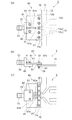
- FIG. 2 is a diagram for explaining the power feeding unit 20 of the film antenna 1 to which the present embodiment is applied.
- the power feeding unit 20 includes a power feeding substrate 21 to which the coaxial cable 30 is connected, and a pressing member 23 that presses the contact 13 of the antenna unit 10 against the power feeding substrate 21.
- the power feeding unit 20 is provided with a male screw (screw) 24 and a female screw (nut) 25.
- the pressing member 23 sandwiches the region having the contact 13 of the antenna unit 10 (the protruding portion 11a formed at one end of the film 11 (upper portion in FIG. 2)) together with the power supply substrate 21 so that the contact 13 and the power supply substrate 21 are sandwiched. Are electrically connected.
- the pressing member 23 is provided with a plurality of through holes, and is pressed using a male screw (screw) 24 and a female screw (nut) 25 to contact the contact 13 of the antenna unit 10 and the power supply board. 21 is electrically connected.
- the contact point 13 is formed on the surface of the protruding portion 11a of the film 11 that faces the power supply substrate 21 (in FIG. 2, the back side of the protruding portion 11a).
- the contact 13 of the antenna unit 10 is provided with an antenna contact 13a that is electrically connected to the dual frequency antenna 12a of the antenna 12 and a GND contact 13b that is electrically connected to the antenna GND 12b of the antenna 12.
- the projecting portion 11 a of the film 11 is provided with a through hole 11 b through which a male screw (screw) 24 passes.
- the through-hole 11b is provided corresponding to each formation location of the antenna contact 13a and the GND contact 13b. In the example shown in FIG.
- the number of through holes 11b is not limited to the above number.
- the size of the antenna contact 13a or the GND contact 13b may be adjusted, and when the antenna contact 13a or the GND contact 13b is small, at least one is necessary, but when the antenna contact 13a or GND contact 13b is large, there may be three or more.
- the power supply board 21 is a glass epoxy board such as FR-4 (Flame Retardant 4) or CEM-3 (Composite Epoxy material 3), and is on the surface facing the contact 13 of the antenna unit 10.
- the pattern is formed of copper.
- the power supply substrate 21 is formed with a power supply substrate antenna power supply portion 21a in the center and a power supply substrate GND portion 21b that is insulated from the power supply substrate antenna power supply portion 21a around the power supply substrate antenna power supply portion 21a. More specifically, the power supply board antenna power supply part 21a faces the antenna contact 13a and the power supply board GND part 21b faces the GND contact 13b below the approximate center of the power supply board 21.
- one through hole 21c is provided in the power supply substrate antenna power supply portion 21a, and four through holes 21c are provided on the power supply substrate GND portion 21b. .
- the through hole 21 c is provided corresponding to the through hole 11 b of the film 11.
- An area for fixing the coaxial cable 30 is secured above the approximate center of the power supply substrate 21.
- the coaxial cable 30 is soldered in a region above the power supply substrate 21. More specifically, the feeding board antenna feeding section 21 a provided at the center on the feeding board 21 and the core wire 31 of the coaxial cable 30 are joined by the solder 41, and the feeding board GND section 21 b on the feeding board 21 and the coaxial cable 30 are connected. The outer conductor 32 is joined by solder 42.
- the coaxial cable 30 is soldered to the power supply board 21 in advance, and then pressed to electrically connect the contact 13 of the antenna unit 10 and the power supply board 21, so that soldering is performed during the soldering process.
- the heat given to the attachment portion is not transmitted to the film 11. Therefore, even when a resin film having a low heat resistance with respect to the film 11 is used, for example, the film 11 is not affected by heat generated during soldering.
- a conductive paste is used as one of the conductive materials on the contact 13 formed on the projecting portion 11a of the film 11 in the antenna portion 10 where the antenna contact 13a and the GND contact 13b are formed.
- a certain silver paste 22 is formed.
- the silver paste 22 is provided on the side where the contact 13 on the side (the back side in FIG. 2) of the protruding portion 11a of the film 11 that faces the power supply substrate 21 is formed.
- the silver paste power distribution unit 22a and the silver paste GND unit The area is divided into 22b and applied.
- the silver paste 22 is applied to the contact 13 by printing, for example. By applying the silver paste 22, the conductivity between the contact 13 and the power supply substrate 21 can be increased.
- the silver paste 22 is used as an example of the intervening conductive material.
- the material is not limited to the silver paste 22, and other materials may be used as long as the conductivity is high and the material is a paste.
- the position of the contact with the silver paste 22 at the contact 13 of the antenna unit 10 is aligned with the contact of the power supply substrate 21. More specifically, the silver paste power distribution unit 22a and the power supply substrate antenna power supply unit 21a of the power supply substrate 21 are combined, the silver paste GND unit 22b and the power supply substrate GND unit 21b of the power supply substrate 21 are combined, and the through hole of the film 11 11b and the through-hole 21c of the electric power feeding board 21 are aligned.
- the pressing member 23 is disposed on the side of the film 11 where the contact 13 is not formed, and the male screw (screw) 24 is inserted into the through hole of the pressing member 23, the through hole 11 b of the film 11, and the through hole 21 c of the power supply substrate 21.
- a female screw (nut) 24 is applied to the side of the power supply substrate 21 where the power supply substrate antenna power supply portion 21a and the power supply substrate GND portion 21b are not formed (the back side in FIG. 2), and the male screw 24 is tightened.
- the contact 13 coated with the silver paste 22 is pressed by the power supply substrate 21 and the pressing member 23, and the antenna contact 13a and the power supply substrate antenna power supply portion 21a, and the GND contact 13b and the power supply substrate GND portion 21b are connected. Connect electrically.
- the 7th-order PIM level appearing in the 800 MHz band is “ ⁇ 82 dBm” before the countermeasure and “ ⁇ 129 dBm” after the countermeasure.
- the distortion component of “47 dB” was improved.
- the 19th-order PIM level appearing in the 2.1 GHz band was “ ⁇ 110 dBm” before the countermeasure and “ ⁇ 135 dBm” after the countermeasure, and the distortion component of “25 dB” was improved.
- the PIM characteristics are improved and a more stable state can be obtained.
- FIGS. 3A to 3C are diagrams showing the configuration of the film antenna 2 to which the second embodiment is applied.
- 3B is a view of the film antenna 2 as viewed from one direction
- FIG. 3A is a view of FIG. 3B from above
- FIG. 3C is a view of FIG. 3B from below. It is a figure.
- the film antenna 2 differs from the film antenna 1 according to the first embodiment in that a connector 70 is connected instead of the coaxial cable 30. Because of this difference, a power feeding unit 60 is provided instead of the power feeding unit 20 of the first embodiment.
- the same functions as those of the first embodiment are denoted by the same reference numerals, and detailed description thereof is omitted here.
- the film antenna 2 to which the second embodiment is applied also functions as one of the flexible printed circuit board structures, and includes a power feeding unit 60 to which a connector 70 for feeding power to the antenna unit 10 is connected. Yes.
- the power feeding section 60 has a power feeding board 61 to which the connector 70 is connected, and presses the contact 13 of the antenna section 10 with the power feeding board 61 and the pressing member 23.
- the power supply section 60 is provided with a male screw (screw) 24 and a female screw (nut) 25.
- the contact point 13 is formed on the surface on the side facing the power supply substrate 61 at the protruding portion 11 a of the film 11.
- the structure of the contact 13 is the same as that of the first embodiment.
- the pressing member 23, male screw (screw) 24, and female screw (nut) 25 are the same as those in the first embodiment.
- the power supply board 61 is formed of, for example, a microstrip line having an impedance of about 50 ⁇ , a transmission line 61d for power supply is provided on the upper surface (front surface), and a conductor is provided on the lower surface (back surface).
- the power supply substrate GND part 61b is formed.
- the power supply substrate GND portion 61b and the power supply substrate antenna power supply portion 61a, which are conductors on the lower surface, are insulated.
- the transmission line 61d on the upper surface of the power supply substrate 61 and the power supply substrate antenna power supply portion 61a on the lower surface are connected via a through hole 61e.
- the power supply substrate antenna power supply portion 61a and the power supply substrate GND portion 61b of the power supply substrate 61 are opposed to the contact 13 of the film 11 at one end of the power supply substrate 61 on the right side of the drawings in FIGS. 3 (a) to 3 (c). Yes.
- the feed board antenna feed section 61a and the feed board GND section 61b facing the contact 13 are provided with through holes 61c corresponding to the through holes (not shown here) of the film 11. More specifically, one through hole 61c is provided in the power supply substrate antenna power supply portion 61a, and two through holes 61c are provided on the left and right sides in the power supply substrate GND portion 61b.
- the connector 70 used for the film antenna 2 for example, a screw-type male connector or the like can be adopted, and a screw portion 72 is provided on one end side thereof, and an external cable (not shown) is connected via the screw portion 72. Connect. The other end of the connector 70 is connected to the conductive plate 80.
- the screw portion 72 and the conductive plate 80 of the connector 70 function as a GND line.
- the conductive plate 80 is composed of a highly conductive material such as copper, for example, and has an L shape in the example shown in FIGS. 3A to 3C.
- the conductive plate 80 is connected to the connector 70 at the vertical start in FIG. 3B, and is connected to the power supply board GND portion 61b of the power supply board 61 in the L-shaped inner horizontal direction.
- the conductive plate 80 and the power supply board GND portion 61b are fixed by screws 81.
- a signal line 71 extends from the connector 70, and the signal line 71 is joined to the transmission line 61 d on the upper surface of the power supply substrate 61 by solder 41.
- the silver paste 22 which is one of the conductive materials is formed on the contact 13 formed on the protruding portion 11a of the film 11 in the antenna unit 10.
- the silver paste 22 is applied to the side where the contact 13 on the side facing the power supply substrate 21 of the protruding portion 11a of the film 11 is formed, for example, by printing.
- the silver paste power distribution unit 22a and the silver paste GND unit 22b described with reference to FIG. 2 are divided into similar structures.
- the power supply substrate 61 and the pressing member 23 are pressed using a male screw (screw) 24 and a female screw (nut) 25, and the contact 13 and the power supply substrate 61 are electrically connected via the silver paste 22. Yes.
- the GND of the conductive plate 80 and the connector 70 is joined according to the structure of the connector 70, for example, by screwing. Further, the signal line 71 of the connector 70 is protruded inside the L-shaped structure of the conductive plate 80 while being insulated from the conductive plate 80. After that, after aligning the conductive plate 80 and the power supply substrate GND portion 61b of the power supply substrate 61, the power supply substrate 61 and the conductive plate 80 are fixed with screws 81, and the power supply substrate GND portion 61b and the conductive plate 80 are electrically connected. Connect to. Further, the signal line 71 of the connector 70 and the transmission line 61 d of the power supply substrate 61 are aligned and soldered, and these are electrically connected by the solder 41.
- a pressing member 23 is disposed on the side of the film 11 where the contact 13 is not formed, and is pressed and fixed by a male screw (screw) 24 and a female screw (nut) 25, and the antenna contact 13a and the power feeding board antenna power supply.
- the portion 61a, the GND contact 13b, and the power supply substrate GND portion 61b are electrically connected.
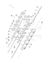
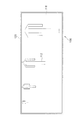
- FIG. 4 is a view showing an embodiment in which the film antenna 1 of the first embodiment or the film antenna 2 of the second embodiment is applied to a vertical smoke barrier 100 as one of indoor partition walls.
- the indoor partition wall in addition to the vertical smoke barrier 100 shown in FIG. 4, for example, it can be applied to a partition partition plate or the like.
- a ceiling installation type antenna or a ceiling embedded type antenna has been used (for example, refer to Japanese Patent Laid-Open No. 9-238812).
- MIMO multiple-input and multiple-output
- An object of the present invention to which the present embodiment is applied is to provide an antenna device that improves the efficiency of installation work without impairing the scenery indoors.
- a vertical smoke barrier 100 is provided in the office 500 for reducing accidents caused by smoke during a fire.
- the vertical smoke barrier 100 is installed with a height vertically downward from the ceiling surface 600 and a length along the ceiling surface 600 so as not to diffuse smoke generated by a fire.
- the antenna is placed at a high place in the room in order to transmit and receive signals throughout the room of the office 500.
- the vertical smoke barrier 100 is provided with an antenna function, it is possible to provide the antenna function together with the function of diffusing smoke and reducing the installation cost without damaging the landscape.
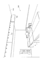
- FIG. 5 is a view for explaining the entire structure of the vertical smoke barrier 100.
- FIG. 6 is a view for explaining a joint portion of the vertical smoke barrier 100.
- the vertical smoke barrier 100 shown in FIG. 5 and FIG. 6 uses a film antenna 110 made of a transparent film made of a resin having a relatively high permeability as a partition material that is formed of a film material or a plate material and partitions an indoor space. Yes.
- An antenna 112 using a transparent conductive material is formed on the film antenna 110.
- the antenna 112 includes, for example, a dual-frequency shared antenna 112a that shares two frequencies of an 800 MHz band and a 2.1 GHz band, and an antenna GND section (not shown) connected to the ground (GND).
- a plurality of (for example, four) antennas 112 are provided, and extend downward from the ceiling surface 600 side as shown in FIG.
- An end 120 is provided around the film antenna 110 as a partition member, and a cover member 121 is provided along the end 120 as shown in FIG.
- An antenna GND part (not shown) is formed on the film antenna 110 in a position hidden by the cover member 121.
- the cover member 121 is formed of a resin material or a metal material, and has a structure in which the cover member 121 and the antenna GND portion are insulated.
- a power supply unit 130 having the same function and structure as the power supply unit 20 or the power supply unit 60 described in detail with reference to FIGS.
- a cable 140 is connected to the power supply unit 130, and the cable 140 and the antenna 112 are electrically connected via the power supply unit 130.
- the wiring structure and the like may be partially different from those of the power feeding unit 20 or the power feeding unit 60, they have substantially the same configuration. That is, the cable 140 and the power supply board (not shown) of the power supply unit 60 are connected by, for example, soldering.
- a conductive material (not shown) made of, for example, silver paste is interposed between the contact point (not shown) of the antenna 112 and the power supply substrate, and is pressed by a pressing member (not shown), The contact point of the antenna 112 and the power supply substrate are electrically connected.
- the other detailed contents are the same as those described with reference to FIGS. 1 to 3, and the description thereof is omitted here.
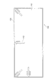
- FIG. 7 and 8 are diagrams showing other examples of the vertical smoke barrier 100.
- FIG. 7 Although the antenna 112 similar to the vertical smoke barrier 100 shown in FIGS. 5 and 6 is provided, the example shown in FIG. 7 can cope with a plurality of polarized waves, and the example shown in FIG. Then, it is possible to cope with a number of frequency bands. More specifically, in the example shown in FIG. 7, the vertical polarization whose electric field plane is perpendicular to the ground, the horizontal polarization which is horizontal, and the +45 degree polarization whose polarization plane is deviated by 45 degrees in the example shown in FIG. It corresponds to 45 degree polarization. In the example shown in FIG.
Landscapes
- Engineering & Computer Science (AREA)
- Architecture (AREA)
- Physics & Mathematics (AREA)
- Electromagnetism (AREA)
- Civil Engineering (AREA)
- Structural Engineering (AREA)
- Details Of Aerials (AREA)
- Support Of Aerials (AREA)
Abstract
Priority Applications (4)
| Application Number | Priority Date | Filing Date | Title |
|---|---|---|---|
| US16/088,515 US10487498B2 (en) | 2016-03-28 | 2017-02-16 | Flexible printed circuit board structure and indoor partition wall |
| CN201780020553.5A CN109075440B (zh) | 2016-03-28 | 2017-02-16 | 柔性印刷电路板结构体及室内分隔壁 |
| EP17773796.2A EP3439106B1 (fr) | 2016-03-28 | 2017-02-16 | Structure de carte de circuit imprimé souple et paroi de séparation intérieure |
| KR1020187028188A KR102073505B1 (ko) | 2016-03-28 | 2017-02-16 | 플렉시블 프린트 기판 구조체, 및 실내 구획벽 |
Applications Claiming Priority (2)
| Application Number | Priority Date | Filing Date | Title |
|---|---|---|---|
| JP2016-064730 | 2016-03-28 | ||
| JP2016064730A JP6317385B2 (ja) | 2016-03-28 | 2016-03-28 | フレキシブルプリント基板構造体、および室内仕切壁 |
Publications (1)
| Publication Number | Publication Date |
|---|---|
| WO2017169248A1 true WO2017169248A1 (fr) | 2017-10-05 |
Family
ID=59964102
Family Applications (1)
| Application Number | Title | Priority Date | Filing Date |
|---|---|---|---|
| PCT/JP2017/005701 Ceased WO2017169248A1 (fr) | 2016-03-28 | 2017-02-16 | Structure de carte de circuit imprimé souple et paroi de séparation intérieure |
Country Status (6)
| Country | Link |
|---|---|
| US (1) | US10487498B2 (fr) |
| EP (1) | EP3439106B1 (fr) |
| JP (1) | JP6317385B2 (fr) |
| KR (1) | KR102073505B1 (fr) |
| CN (1) | CN109075440B (fr) |
| WO (1) | WO2017169248A1 (fr) |
Families Citing this family (4)
| Publication number | Priority date | Publication date | Assignee | Title |
|---|---|---|---|---|
| KR102182492B1 (ko) * | 2017-02-06 | 2020-11-24 | 니혼덴교고사꾸가부시끼가이샤 | 안테나 구조체 |
| CN113193339B (zh) * | 2021-03-22 | 2023-01-10 | 安徽精卓光显技术有限责任公司 | 一种透明室分吸顶天线 |
| KR20230032305A (ko) * | 2021-08-30 | 2023-03-07 | 주식회사 센서뷰 | 투명 안테나 |
| EP4552181A1 (fr) * | 2022-09-20 | 2025-05-14 | AGC Glass Europe | Appareil et procédés et utilisations associés |
Citations (8)
| Publication number | Priority date | Publication date | Assignee | Title |
|---|---|---|---|---|
| JPS63254804A (ja) * | 1987-04-10 | 1988-10-21 | Yagi Antenna Co Ltd | アンテナ給電装置 |
| JPS6449302A (en) * | 1987-08-19 | 1989-02-23 | Dainippon Printing Co Ltd | Film antenna |
| JPH0455810U (fr) * | 1990-09-18 | 1992-05-13 | ||
| JP2006287729A (ja) * | 2005-04-01 | 2006-10-19 | Nissha Printing Co Ltd | 建築物窓用透明アンテナ、及びアンテナ付き建築物窓用透光性部材 |
| JP2008187383A (ja) * | 2007-01-29 | 2008-08-14 | Maspro Denkoh Corp | フィルムアンテナ、電源供給装置、及び移動体用受信システム |
| JP2010034924A (ja) * | 2008-07-30 | 2010-02-12 | Kojima Press Industry Co Ltd | 車載用アンテナ |
| JP2011091556A (ja) * | 2009-10-21 | 2011-05-06 | Panasonic Corp | アンテナ装置 |
| JP2013255094A (ja) * | 2012-06-07 | 2013-12-19 | Harada Ind Co Ltd | アンテナ給電装置 |
Family Cites Families (23)
| Publication number | Priority date | Publication date | Assignee | Title |
|---|---|---|---|---|
| JPH0611083B2 (ja) * | 1987-04-10 | 1994-02-09 | 八木アンテナ株式会社 | アンテナ装置 |
| KR900009111B1 (ko) | 1986-11-07 | 1990-12-22 | 야기 안테나 가부시기가이샤 | 필름형 안테나 장치 |
| JP3204347B2 (ja) | 1993-07-15 | 2001-09-04 | キヤノン株式会社 | 光学素子の成形装置 |
| JPH0733452U (ja) | 1993-11-30 | 1995-06-20 | 愛知製鋼株式会社 | 取鍋走行台車 |
| JPH09238012A (ja) | 1996-02-29 | 1997-09-09 | Matsushita Electric Works Ltd | アンテナ装置 |
| CN2259642Y (zh) * | 1996-04-12 | 1997-08-13 | 鸿海精密工业股份有限公司 | 接通存储卡连接器与主电路板的连接装置 |
| FR2748862B1 (fr) * | 1996-05-17 | 1998-07-17 | Radiall Sa | Dispositif pour raccorder un cable coaxial a une carte de circuit imprime |
| JP4350247B2 (ja) * | 1999-12-27 | 2009-10-21 | 原田工業株式会社 | フィルムアンテナ |
| CN1293674C (zh) | 2001-02-05 | 2007-01-03 | 索尼公司 | 低姿态小型天线及其构造方法 |
| US6548762B2 (en) * | 2001-02-21 | 2003-04-15 | Andrew Corporation | Transmission line grounding lug |
| JP4076931B2 (ja) * | 2003-09-02 | 2008-04-16 | 日本アンテナ株式会社 | アンテナ給電部 |
| US7322833B1 (en) * | 2006-10-31 | 2008-01-29 | Flextronics Ap, Llc | Connection of FPC antenna to PCB |
| JP4281116B2 (ja) * | 2007-04-27 | 2009-06-17 | 日本電気株式会社 | 給電装置 |
| KR100960018B1 (ko) * | 2007-11-29 | 2010-05-28 | 한국전자통신연구원 | 다중공진을 이용한 비분산 특성의 초광대역 안테나 장치 |
| KR101217650B1 (ko) * | 2009-07-02 | 2013-01-04 | 주식회사 프로이천 | 보드 커넥터 |
| CN102201613A (zh) * | 2010-03-24 | 2011-09-28 | 孙全辉 | 多频段吸顶天线 |
| JP5555610B2 (ja) * | 2010-11-19 | 2014-07-23 | 日本板硝子株式会社 | 端子、端子付ガラス板及び移動体用端子付ガラス板 |
| JP5708519B2 (ja) * | 2012-02-03 | 2015-04-30 | 株式会社デンソー | 太陽電池一体型アンテナ |
| CN103151605B (zh) * | 2012-03-31 | 2015-06-17 | 深圳光启创新技术有限公司 | Wi-Fi吸顶天线装置 |
| JP2013254804A (ja) * | 2012-06-06 | 2013-12-19 | Ps4 Luxco S A R L | 半導体装置及びその製造方法 |
| US9742060B2 (en) * | 2014-08-06 | 2017-08-22 | Michael Clyde Walker | Ceiling assembly with integrated repeater antenna |
| US10024883B2 (en) * | 2015-03-27 | 2018-07-17 | Yokowo Co., Ltd. | Contact unit and inspection jig |
| CN204968248U (zh) * | 2015-10-09 | 2016-01-13 | 河北工程技术高等专科学校 | 一种柔性电路板夹具 |
-
2016
- 2016-03-28 JP JP2016064730A patent/JP6317385B2/ja active Active
-
2017
- 2017-02-16 WO PCT/JP2017/005701 patent/WO2017169248A1/fr not_active Ceased
- 2017-02-16 KR KR1020187028188A patent/KR102073505B1/ko active Active
- 2017-02-16 CN CN201780020553.5A patent/CN109075440B/zh active Active
- 2017-02-16 EP EP17773796.2A patent/EP3439106B1/fr active Active
- 2017-02-16 US US16/088,515 patent/US10487498B2/en active Active
Patent Citations (8)
| Publication number | Priority date | Publication date | Assignee | Title |
|---|---|---|---|---|
| JPS63254804A (ja) * | 1987-04-10 | 1988-10-21 | Yagi Antenna Co Ltd | アンテナ給電装置 |
| JPS6449302A (en) * | 1987-08-19 | 1989-02-23 | Dainippon Printing Co Ltd | Film antenna |
| JPH0455810U (fr) * | 1990-09-18 | 1992-05-13 | ||
| JP2006287729A (ja) * | 2005-04-01 | 2006-10-19 | Nissha Printing Co Ltd | 建築物窓用透明アンテナ、及びアンテナ付き建築物窓用透光性部材 |
| JP2008187383A (ja) * | 2007-01-29 | 2008-08-14 | Maspro Denkoh Corp | フィルムアンテナ、電源供給装置、及び移動体用受信システム |
| JP2010034924A (ja) * | 2008-07-30 | 2010-02-12 | Kojima Press Industry Co Ltd | 車載用アンテナ |
| JP2011091556A (ja) * | 2009-10-21 | 2011-05-06 | Panasonic Corp | アンテナ装置 |
| JP2013255094A (ja) * | 2012-06-07 | 2013-12-19 | Harada Ind Co Ltd | アンテナ給電装置 |
Non-Patent Citations (1)
| Title |
|---|
| See also references of EP3439106A4 * |
Also Published As
| Publication number | Publication date |
|---|---|
| KR102073505B1 (ko) | 2020-02-04 |
| KR20180116414A (ko) | 2018-10-24 |
| JP6317385B2 (ja) | 2018-04-25 |
| CN109075440A (zh) | 2018-12-21 |
| EP3439106A1 (fr) | 2019-02-06 |
| EP3439106A4 (fr) | 2019-11-13 |
| US10487498B2 (en) | 2019-11-26 |
| US20190112806A1 (en) | 2019-04-18 |
| EP3439106C0 (fr) | 2023-06-07 |
| JP2017183850A (ja) | 2017-10-05 |
| CN109075440B (zh) | 2021-06-01 |
| EP3439106B1 (fr) | 2023-06-07 |
Similar Documents
| Publication | Publication Date | Title |
|---|---|---|
| CN109802234B (zh) | 基站天线及移相馈电装置 | |
| JP7239743B2 (ja) | アンテナユニット及び端末機器 | |
| US20140102763A1 (en) | Rigid flexible circuit board with impedance control | |
| JP6317385B2 (ja) | フレキシブルプリント基板構造体、および室内仕切壁 | |
| CN112909560B (zh) | 液晶天线及其制作方法 | |
| WO2020155723A1 (fr) | Appareil d'alimentation à déphasage et antenne de station de base | |
| CN106876969A (zh) | 一种天线及无线信号收发系统 | |
| EP3336964A1 (fr) | Câble imprimé et son procédé de fabrication, câble de connexion, et système d'antenne accordée électriquement | |
| US6133877A (en) | Microstrip distribution network device for antennas | |
| CN113644422B (zh) | 一种柔性传输线与天线一体化组件 | |
| US9408306B2 (en) | Antenna array feeding structure having circuit boards connected by at least one solderable pin | |
| EP4145627A1 (fr) | Panneau interactif | |
| TWI451628B (zh) | 具有天線結構之電子設備 | |
| CN209329161U (zh) | 移相馈电装置及基站天线 | |
| CN209329160U (zh) | 基站天线及其移相馈电装置 | |
| CN211376931U (zh) | 天线组件和基站天线 | |
| CN205960360U (zh) | 射频连接器 | |
| CN216720291U (zh) | 一种天线组件和电子设备 | |
| US11621464B2 (en) | Waveguide assembly | |
| US9614268B2 (en) | Anti-lightning combined-stripline-circuit system | |
| KR102109621B1 (ko) | 3차원 방송 안테나 | |
| US12412997B2 (en) | Electronic device and antenna module | |
| US20250202131A1 (en) | Integrated antenna array with feed and calibration networks | |
| CN217740387U (zh) | 一种按键组件和电子设备 | |
| CN117154408A (zh) | 毫米波天线组件以及显示装置 |
Legal Events
| Date | Code | Title | Description |
|---|---|---|---|
| ENP | Entry into the national phase |
Ref document number: 20187028188 Country of ref document: KR Kind code of ref document: A |
|
| NENP | Non-entry into the national phase |
Ref country code: DE |
|
| WWE | Wipo information: entry into national phase |
Ref document number: 2017773796 Country of ref document: EP |
|
| ENP | Entry into the national phase |
Ref document number: 2017773796 Country of ref document: EP Effective date: 20181029 |
|
| 121 | Ep: the epo has been informed by wipo that ep was designated in this application |
Ref document number: 17773796 Country of ref document: EP Kind code of ref document: A1 |