WO2017175035A1 - Capteur de pression constituant une pluralité de canaux, dispositif d'entrée tactile le comprenant, et procédé de détection de pression dans lequel ce dernier est utilisé - Google Patents
Capteur de pression constituant une pluralité de canaux, dispositif d'entrée tactile le comprenant, et procédé de détection de pression dans lequel ce dernier est utilisé Download PDFInfo
- Publication number
- WO2017175035A1 WO2017175035A1 PCT/IB2016/051998 IB2016051998W WO2017175035A1 WO 2017175035 A1 WO2017175035 A1 WO 2017175035A1 IB 2016051998 W IB2016051998 W IB 2016051998W WO 2017175035 A1 WO2017175035 A1 WO 2017175035A1
- Authority
- WO
- WIPO (PCT)
- Prior art keywords
- touch
- pressure
- input device
- channel
- electrode
- Prior art date
- Legal status (The legal status is an assumption and is not a legal conclusion. Google has not performed a legal analysis and makes no representation as to the accuracy of the status listed.)
- Ceased
Links
Images



























Classifications
-
- G—PHYSICS
- G06—COMPUTING OR CALCULATING; COUNTING
- G06F—ELECTRIC DIGITAL DATA PROCESSING
- G06F3/00—Input arrangements for transferring data to be processed into a form capable of being handled by the computer; Output arrangements for transferring data from processing unit to output unit, e.g. interface arrangements
- G06F3/01—Input arrangements or combined input and output arrangements for interaction between user and computer
- G06F3/03—Arrangements for converting the position or the displacement of a member into a coded form
- G06F3/041—Digitisers, e.g. for touch screens or touch pads, characterised by the transducing means
- G06F3/044—Digitisers, e.g. for touch screens or touch pads, characterised by the transducing means by capacitive means
- G06F3/0445—Digitisers, e.g. for touch screens or touch pads, characterised by the transducing means by capacitive means using two or more layers of sensing electrodes, e.g. using two layers of electrodes separated by a dielectric layer
-
- G—PHYSICS
- G06—COMPUTING OR CALCULATING; COUNTING
- G06F—ELECTRIC DIGITAL DATA PROCESSING
- G06F3/00—Input arrangements for transferring data to be processed into a form capable of being handled by the computer; Output arrangements for transferring data from processing unit to output unit, e.g. interface arrangements
- G06F3/01—Input arrangements or combined input and output arrangements for interaction between user and computer
- G06F3/03—Arrangements for converting the position or the displacement of a member into a coded form
- G06F3/041—Digitisers, e.g. for touch screens or touch pads, characterised by the transducing means
- G06F3/0416—Control or interface arrangements specially adapted for digitisers
- G06F3/04164—Connections between sensors and controllers, e.g. routing lines between electrodes and connection pads
-
- G—PHYSICS
- G06—COMPUTING OR CALCULATING; COUNTING
- G06F—ELECTRIC DIGITAL DATA PROCESSING
- G06F3/00—Input arrangements for transferring data to be processed into a form capable of being handled by the computer; Output arrangements for transferring data from processing unit to output unit, e.g. interface arrangements
- G06F3/01—Input arrangements or combined input and output arrangements for interaction between user and computer
- G06F3/03—Arrangements for converting the position or the displacement of a member into a coded form
- G06F3/041—Digitisers, e.g. for touch screens or touch pads, characterised by the transducing means
- G06F3/0416—Control or interface arrangements specially adapted for digitisers
- G06F3/0418—Control or interface arrangements specially adapted for digitisers for error correction or compensation, e.g. based on parallax, calibration or alignment
-
- G—PHYSICS
- G06—COMPUTING OR CALCULATING; COUNTING
- G06F—ELECTRIC DIGITAL DATA PROCESSING
- G06F3/00—Input arrangements for transferring data to be processed into a form capable of being handled by the computer; Output arrangements for transferring data from processing unit to output unit, e.g. interface arrangements
- G06F3/01—Input arrangements or combined input and output arrangements for interaction between user and computer
- G06F3/03—Arrangements for converting the position or the displacement of a member into a coded form
- G06F3/041—Digitisers, e.g. for touch screens or touch pads, characterised by the transducing means
- G06F3/044—Digitisers, e.g. for touch screens or touch pads, characterised by the transducing means by capacitive means
- G06F3/0446—Digitisers, e.g. for touch screens or touch pads, characterised by the transducing means by capacitive means using a grid-like structure of electrodes in at least two directions, e.g. using row and column electrodes
-
- G—PHYSICS
- G06—COMPUTING OR CALCULATING; COUNTING
- G06F—ELECTRIC DIGITAL DATA PROCESSING
- G06F2203/00—Indexing scheme relating to G06F3/00 - G06F3/048
- G06F2203/041—Indexing scheme relating to G06F3/041 - G06F3/045
- G06F2203/04105—Pressure sensors for measuring the pressure or force exerted on the touch surface without providing the touch position
-
- G—PHYSICS
- G06—COMPUTING OR CALCULATING; COUNTING
- G06F—ELECTRIC DIGITAL DATA PROCESSING
- G06F3/00—Input arrangements for transferring data to be processed into a form capable of being handled by the computer; Output arrangements for transferring data from processing unit to output unit, e.g. interface arrangements
- G06F3/01—Input arrangements or combined input and output arrangements for interaction between user and computer
- G06F3/03—Arrangements for converting the position or the displacement of a member into a coded form
- G06F3/041—Digitisers, e.g. for touch screens or touch pads, characterised by the transducing means
- G06F3/0412—Digitisers structurally integrated in a display
-
- G—PHYSICS
- G06—COMPUTING OR CALCULATING; COUNTING
- G06F—ELECTRIC DIGITAL DATA PROCESSING
- G06F3/00—Input arrangements for transferring data to be processed into a form capable of being handled by the computer; Output arrangements for transferring data from processing unit to output unit, e.g. interface arrangements
- G06F3/01—Input arrangements or combined input and output arrangements for interaction between user and computer
- G06F3/03—Arrangements for converting the position or the displacement of a member into a coded form
- G06F3/041—Digitisers, e.g. for touch screens or touch pads, characterised by the transducing means
- G06F3/0414—Digitisers, e.g. for touch screens or touch pads, characterised by the transducing means using force sensing means to determine a position
- G06F3/04144—Digitisers, e.g. for touch screens or touch pads, characterised by the transducing means using force sensing means to determine a position using an array of force sensing means
-
- G—PHYSICS
- G06—COMPUTING OR CALCULATING; COUNTING
- G06F—ELECTRIC DIGITAL DATA PROCESSING
- G06F3/00—Input arrangements for transferring data to be processed into a form capable of being handled by the computer; Output arrangements for transferring data from processing unit to output unit, e.g. interface arrangements
- G06F3/01—Input arrangements or combined input and output arrangements for interaction between user and computer
- G06F3/03—Arrangements for converting the position or the displacement of a member into a coded form
- G06F3/041—Digitisers, e.g. for touch screens or touch pads, characterised by the transducing means
- G06F3/0416—Control or interface arrangements specially adapted for digitisers
- G06F3/0418—Control or interface arrangements specially adapted for digitisers for error correction or compensation, e.g. based on parallax, calibration or alignment
- G06F3/04182—Filtering of noise external to the device and not generated by digitiser components
Definitions
- the present invention relates to a pressure sensor that forms a plurality of channels for pressure detection, and a touch input device including the pressure sensor. More specifically, the present invention is applied to a touch input device configured to be able to detect a touch position.
- the present invention relates to a pressure sensor that constitutes a plurality of channels that can detect pressure, a touch input device including the same, and a pressure detection method using the same.
- the touch screen may constitute a touch surface of a touch input device that includes a touch sensor panel that may be a transparent panel with a touch-sensitive surface.
- a touch sensor panel is attached to the front surface of the display screen, and the touch-sensitive surface can cover the visible surface of the display screen.
- the user can operate the computing system by simply touching the touch screen with a finger or the like.
- a computing system can perform operations accordingly by recognizing touches and touch locations on a touch screen and interpreting such touches. At this time, there is a need for a touch input device that can detect not only the touch position by touch on the touch screen but also the magnitude of the touch pressure.
- An object of the present invention is to provide a pressure sensor that constitutes a plurality of channels for pressure detection, a touch input device including the pressure sensor, and a pressure detection method using the pressure sensor.
- the touch input device is capable of detecting the pressure of the touch on the touch surface, and is arranged at a position where the distance between the display module and the reference potential layer can be changed by the touch on the touch surface. And the distance may vary depending on the magnitude of the pressure of the touch, and the pressure sensor may output a signal including information on a capacitance that varies with the distance.
- a plurality of electrodes are formed to form a plurality of channels, and the magnitude of the pressure on the touch is determined based on the amount of change in capacitance detected in each channel and the SNR improvement scaling factor assigned to each channel. Can be detected.
- a pressure sensor that forms a plurality of channels for pressure detection, a touch input device including the pressure sensor, and a pressure detection method using the pressure sensor.
- a pressure sensor that configures a plurality of channels with high pressure detection accuracy with respect to a touch, and a touch input device including the pressure sensor.
- it is a conceptual diagram illustrating the relative position of the touch sensor panel with respect to the display panel.
- it is a conceptual diagram illustrating the relative position of the touch sensor panel with respect to the display panel.
- it is a conceptual diagram illustrating the relative position of the touch sensor panel with respect to the display panel.
- it is a conceptual diagram illustrating the relative position of the touch sensor panel with respect to the display panel.
- it is a conceptual diagram illustrating the relative position of the touch sensor panel with respect to the display panel.
- 1 is a cross-sectional view of an exemplary pressure sensor including a pressure electrode according to an embodiment of the present invention.
- 1 is a cross-sectional view of an exemplary pressure sensor including a pressure electrode according to an embodiment of the present invention.
- 1 is a cross-sectional view of an exemplary pressure sensor including a pressure electrode according to an embodiment of the present invention.
- 1 is a cross-sectional view of an exemplary pressure sensor including a pressure electrode according to an embodiment of the present invention.
- 1 is a cross-sectional view of an exemplary pressure sensor including a pressure electrode according to an embodiment of the present invention.
- 1 is a cross-sectional view of an exemplary pressure sensor including a pressure electrode according to an embodiment of the present invention.
- 1 is a cross-sectional view of an exemplary pressure sensor including a pressure electrode according to an embodiment of the present invention.
- 1 is a cross-sectional view of an exemplary pressure sensor including a pressure electrode according to an embodiment of the present invention.
- 4 is a diagram illustrating a change amount of capacitance due to a change in distance between an electrode layer and a reference potential layer according to an embodiment of the present invention.
- 1 is a cross-sectional view of a touch input device of a first example to which a pressure sensor and a pressure detection module according to an embodiment of the present invention can be applied. In the touch input device according to the embodiment of the present invention, the optical layer of the backlight unit is illustrated.
- positioning of the pressure sensor of the 3rd example contained in the touch input device is illustrated. It is sectional drawing of a part of touch input device with which the pressure sensor was attached to the touch input device by the 1st method. It is a top view of the pressure sensor for attaching a pressure sensor to a touch input device by the 1st method. It is sectional drawing of a part of touch input device with which the pressure sensor was attached to the touch input device by the 2nd method. 6 illustrates a pressure electrode pattern included in a pressure sensor for pressure detection according to an embodiment of the present invention. 6 illustrates a pressure electrode pattern included in a pressure sensor for pressure detection according to an embodiment of the present invention.
- 6 illustrates a pressure electrode pattern included in a pressure sensor for pressure detection according to an embodiment of the present invention.
- 6 illustrates a pressure electrode pattern included in a pressure sensor for pressure detection according to an embodiment of the present invention.
- 6 illustrates a pressure electrode pattern included in a pressure sensor for pressure detection according to an embodiment of the present invention.
- 4 illustrates a relationship between the magnitude of a touch pressure and a saturation area in a touch input device to which a pressure sensor according to an embodiment of the present invention is applied.
- 4 illustrates a relationship between the magnitude of a touch pressure and a saturation area in a touch input device to which a pressure sensor according to an embodiment of the present invention is applied.
- 2 illustrates a cross section of a pressure sensor according to an embodiment of the present invention.
- 2 illustrates a cross section of a pressure sensor according to an embodiment of the present invention.
- 2 illustrates a cross section of a pressure sensor according to an embodiment of the present invention.
- 2 illustrates a cross section of a pressure sensor according to an embodiment of the present invention.
- 2 illustrates a method for attaching a pressure sensor according to an embodiment of the present invention.
- 2 illustrates a method for attaching a pressure sensor according to an embodiment of the present invention.
- 6 illustrates a method of coupling a pressure sensor to a touch sensing circuit according to an embodiment of the present invention. 6 illustrates a method of coupling a pressure sensor to a touch sensing circuit according to an embodiment of the present invention.
- FIG. 6 illustrates a method of coupling a pressure sensor to a touch sensing circuit according to an embodiment of the present invention.
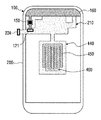
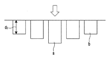
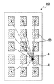
- 1 illustrates a configuration in which a pressure sensor according to an embodiment of the present invention includes a plurality of channels.
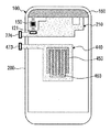
- 1 illustrates a configuration in which a pressure sensor according to an embodiment of the present invention includes a plurality of channels.
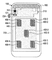
- 1 illustrates a configuration in which a pressure sensor according to an embodiment of the present invention includes a plurality of channels.
- 1 illustrates a configuration in which a pressure sensor according to an embodiment of the present invention includes a plurality of channels. The form of the 1st electrode and the 2nd electrode which are included in the pressure sensor by the embodiment of the present invention is illustrated.
- FIG. 13D is a diagram illustrating a case where pressure is applied to a predetermined position in the pressure sensor illustrated in FIG. 13D.
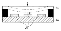
- FIG. 14B is a cross-sectional view illustrating a configuration in which the touch input device bends when a touch pressure is applied to the touch surface corresponding to position A in FIG. 14A.
- FIG. 14B is a cross-sectional view illustrating a configuration in which the touch input device bends when touch pressure is applied to the touch surface corresponding to position C in FIG. 14A.
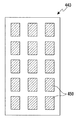
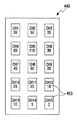
- FIG. 13 is a diagram illustrating scaling factors assigned to the respective first electrodes in the pressure sensor illustrated in FIG. 13D.
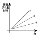
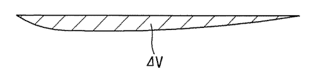
- FIG. 14B is a graph for explaining the relationship between the magnitude of applied pressure and the volume change amount of the touch input device when pressure is applied to the position shown in FIG. 14A.
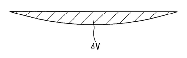
- FIG. 14B is a cross-sectional view illustrating a volume change amount of the touch input device illustrated in FIG. 14B.
- FIG. 14C is a cross-sectional view illustrating a volume change amount of the touch input device illustrated in FIG. 14C.
- FIG. 17b is a cross-sectional view of the drawing shown in FIG. 17b.
- 13 illustrates an equivalent circuit of an apparatus for sensing pressure capacitance with respect to the pressure sensor of the form shown in FIGS. 13a to 13c.
- Fig. 13 illustrates an equivalent circuit of a device for sensing pressure capacitance for the pressure sensor shown in Fig. 13d. It is drawing for demonstrating the case where a pressure is applied to D position of the pressure sensor shown by FIG. 14a.
- FIG. 19a It is a graph for demonstrating that a pressure value is calculated when a pressure is applied to D position shown by FIG. 19a.
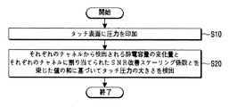
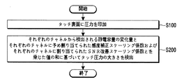
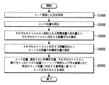
- 5 is a flowchart for explaining an example of a method for detecting the magnitude of a touch pressure using a plurality of channels in a touch input device according to an embodiment of the present invention.
- 5 is a flowchart for explaining an example of a method for detecting the magnitude of a touch pressure using a plurality of channels in a touch input device according to an embodiment of the present invention.
- 5 is a flowchart for explaining an example of a method for detecting the magnitude of a touch pressure using a plurality of channels in a touch input device according to an embodiment of the present invention.
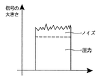
- 17c is a graph showing the magnitude of a signal including information on the capacitance detected in the channel corresponding to the position a in FIG. 17c.
- 17c is a graph showing the magnitude of a signal including information on the capacitance detected in the channel corresponding to the position b in FIG. 17c.
- 6 is a diagram for explaining an SNR improvement scaling factor assigned to each channel when pressure is applied to a P position.
- 6 is a diagram for explaining an SNR improvement scaling factor assigned to each channel when pressure is applied to a P position. It is drawing which shows the variation
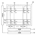
- FIG. 1 is a schematic diagram of a capacitive touch sensor panel 100 included in a touch input device to which a pressure sensor 440 and a pressure detection module including the pressure sensor 440 according to an embodiment of the present invention can be applied, and a configuration for this operation. is there.
- the touch sensor panel 100 includes a plurality of drive electrodes TX1 to TXn and a plurality of reception electrodes RX1 to RXm, and is driven by the plurality of drive electrodes TX1 to TXn for the operation of the touch sensor panel 100.
- Sensing for detecting presence / absence of touch and / or touch position by receiving a sensing signal including information on a change amount of capacitance that changes due to a touch on a touch surface of the touch sensor panel 100 and a driving unit 120 that applies a signal.
- the unit 110 may be included.
- the touch sensor panel 100 may include a plurality of drive electrodes TX1 to TXn and a plurality of reception electrodes RX1 to RXm.
- FIG. 1 shows that the plurality of drive electrodes TX1 to TXn and the plurality of reception electrodes RX1 to RXm of the touch sensor panel 100 form an orthogonal array.
- the electrodes TX1 to TXn and the plurality of receiving electrodes RX1 to RXm can have an arbitrary number of dimensions including a diagonal line, concentric circles, and a three-dimensional random array, and this applied array.
- n and m may have the same or different values as integers of quantities, and the sizes may vary depending on the embodiment.
- the plurality of drive electrodes TX1 to TXn and the plurality of reception electrodes RX1 to RXm may be arranged so as to cross each other.
- the drive electrode TX includes a plurality of drive electrodes TX1 to TXn extending in the first axis direction
- the reception electrode RX includes a plurality of reception electrodes RX1 to RXm extending in the second axis direction intersecting the first axis direction. But you can.
- the plurality of drive electrodes TX1 to TXn and the plurality of reception electrodes RX1 to RXm may be formed in the same layer.
- the plurality of drive electrodes TX1 to TXn and the plurality of reception electrodes RX1 to RXm may be formed on the same surface of an insulating film (not shown).
- the plurality of drive electrodes TX1 to TXn and the plurality of reception electrodes RX1 to RXm may be formed in different layers.
- the plurality of drive electrodes TX1 to TXn and the plurality of reception electrodes RX1 to RXm may be formed on both surfaces of one insulating film (not shown), respectively, or the plurality of drive electrodes TX1 to TXn
- the one insulating film (not shown) and the plurality of receiving electrodes RX1 to RXm may be formed on one surface of a second insulating film (not shown) different from the first insulating film.
- the plurality of drive electrodes TX1 to TXn and the plurality of reception electrodes RX1 to RXm are made of a transparent conductive material (for example, tin oxide (SnO 2 ) And indium oxide (In 2 O 3 ) Or the like made of ITO (Indium Tin Oxide) or ATO (Antimony Tin Oxide).
- a transparent conductive material for example, tin oxide (SnO 2 ) And indium oxide (In 2 O 3 ) Or the like made of ITO (Indium Tin Oxide) or ATO (Antimony Tin Oxide).
- the driving electrode TX and the receiving electrode RX may be formed of other transparent conductive materials or opaque conductive materials.
- the drive electrode TX and the reception electrode RX may be configured to include at least one of silver ink, copper, and carbon nanotube (CNT: Carbon Nanotube).
- the driving electrode TX and the receiving electrode RX may be implemented with a metal mesh or may be made of a silver nano material.
- the driving unit 120 can apply a driving signal to the driving electrodes TX1 to TXn.
- the driving signal may be sequentially applied to one driving electrode at a time from the first driving electrode TX1 to the nth driving electrode TXn. Such application of the driving signal may be repeated again.
- drive signals may be simultaneously applied to multiple drive electrodes according to the embodiment.
- the sensing unit 110 receives a sensing signal including information about the capacitance Cm: 101 generated between the driving electrodes TX1 to TXn and the receiving electrodes RX1 to RXm to which driving signals are applied through the receiving electrodes RX1 to RXm.
- the sensing signal may be a signal obtained by coupling a driving signal applied to the driving electrode TX with a capacitance Cm: 101 generated between the driving electrode TX and the receiving electrode RX.
- the sensing unit 110 may include a receiver (not shown) connected to each of the reception electrodes RX1 to RXm via a switch. The switch is turned on during a time period in which the signal of the reception electrode RX is sensed so that a sensing signal from the reception electrode RX can be sensed by the receiver.
- the receiver may be configured to include an amplifier (not shown) and a feedback capacitor coupled between the negative ( ⁇ ) input of the amplifier and the output of the amplifier, ie, a feedback path.
- the positive (+) input terminal of the amplifier may be connected to a ground or a reference voltage.
- the receiver may further include a reset switch connected in parallel with the feedback capacitor. The reset switch can reset the current to voltage conversion performed by the receiver.
- the negative input terminal of the amplifier is connected to the receiving electrode RX and receives a current signal including information on the capacitance Cm: 101, and then can be integrated and converted into a voltage.
- the sensing unit 110 may further include an ADC (not shown: Analog-Digital Converter) that converts data integrated through the receiver into digital data. Thereafter, the digital data may be input to a processor (not shown) and processed to obtain touch information for the touch sensor panel 100.
- the sensing unit 110 may be configured to include an ADC and a processor together with the receiver.
- the controller 130 can perform a function of controlling the operations of the driving unit 120 and the sensing unit 110. For example, after generating the drive control signal, the control unit 130 can transmit the drive control signal to the drive unit 120 so that the drive signal is applied to the drive electrode TX set in advance at a predetermined time. The controller 130 generates a sensing control signal and then transmits the sensing control signal to the sensing unit 110. The sensing unit 110 receives a sensing signal from the receiving electrode RX set in advance at a predetermined time, and is set in advance. Can perform functions. 1, the driving unit 120 and the sensing unit 110 constitute a touch detection device (not shown) that can detect the presence / absence and / or the touch position of the touch sensor panel 100 according to an embodiment of the present invention. Can do.
- the touch detection device may further include a controller 130.
- the touch detection device may be embodied in a touch input device 1000 including the touch sensor panel 100 by being integrated on a touch sensing IC (touch sensing integrated circuit: not shown) that is a touch sensing circuit. Good.
- the drive electrode TX and the reception electrode RX included in the touch sensor panel 100 may be connected to the touch sensing IC via, for example, a conductive trace and / or a conductive pattern printed on a circuit board.
- the driving unit 120 and the sensing unit 110 may be connected.
- the touch sensing IC can be located on a circuit board on which a conductive pattern is printed.
- the touch sensing IC may be mounted on the main board for the operation of the touch input device 1000.
- an electrostatic capacitance C having a predetermined value is generated at each intersection of the drive electrode TX and the reception electrode RX and an object such as a finger is in proximity to the touch sensor panel 100, such a static capacitance C is generated.
- the capacitance value can be changed.
- the capacitance may represent a mutual capacitance Cm.
- Such electrical characteristics can be sensed by the sensing unit 110 to sense the presence / absence of a touch on the touch sensor panel 100 and / or the touch position.
- the presence / absence of touch and / or the position thereof on the surface of the touch sensor panel 100 formed of a two-dimensional plane including the first axis and the second axis can be detected. More specifically, when the touch to the touch sensor panel 100 occurs, the position of the touch in the second axis direction can be detected by detecting the drive electrode TX to which the drive signal is applied. Similarly, it is possible to detect the position of the touch in the first axis direction by detecting a change in capacitance from a reception signal received via the reception electrode RX when the touch sensor panel 100 is touched. it can. As described above, the mutual capacitive touch sensor panel has been described in detail as the touch sensor panel 100.
- the touch sensor panel for detecting the presence / absence of a touch and the touch position. 100 is a self-capacitance method other than the method described above, a surface capacitance method, a projected capacitance method, a resistive film method, a surface acoustic wave method (SAW), infrared (infrared) System, optical imaging method, dispersive signal technology, and acoustic pulse recognition method. It may be embodied using a switch sensing method.
- a configuration corresponding to the drive electrode TX and the reception electrode RX for detecting presence / absence of touch and / or a touch position may be referred to as a touch sensor.
- the touch sensor panel 100 may be located outside or inside the display panel 200A.
- the display panel 200A of the touch input device 1000 according to the embodiment is a display panel included in a liquid crystal display device (LCD), a PDP (plasma display panel), an organic light emitting display device (Organic Light Emitting Diode: OLED), and the like. It may be. Accordingly, the user can perform an input action by touching the touch surface while visually confirming a screen displayed on the display panel.
- LCD liquid crystal display device
- PDP plasma display panel
- OLED Organic Light Emitting Diode
- the display panel 200A receives an input from a central processing unit (CPU) or an application processor (AP) that is a central processing unit on the main board for operation of the touch input device 1000, and displays the display panel 200A.
- a control circuit for displaying desired contents on the panel may be included.
- a control circuit for operating the display panel 200A may be mounted on a second printed circuit board 210 (hereinafter referred to as a second PCB) in FIGS. 10a to 12c.
- the control circuit for operating the display panel 200A may include a display panel control IC, a graphic control IC, and other circuits necessary for the operation of the display panel 200A.
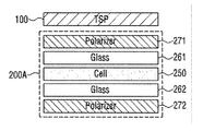
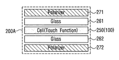
- the LCD panel includes a liquid crystal layer 250 including a liquid crystal cell, first and second substrates 261 and 262 including electrodes at both ends of the liquid crystal layer 250, and The first polarizing layer 271 may be included on one surface of the first substrate 261 and the second polarizing layer 272 may be included on one surface of the second substrate 262 as a direction facing the liquid crystal layer 250.
- the first substrate 261 may be a color filter glass
- the second substrate 262 may be a TFT glass
- the first substrate 261 and / or the second substrate 262 may be a plastic substrate.
- the LCD panel may further include other configurations to perform the display function and can be modified.
- FIG. 2a shows that in the touch input device 1000, the touch sensor panel 100 is disposed outside the display panel 200A.
- the touch surface for the touch input device 1000 may be the surface of the touch sensor panel 100.
- the upper surface of the touch sensor panel 100 may be a touch surface.
- the touch surface for the touch input device 1000 may be the outer surface of the display panel 200A.
- FIG. 1 shows that in the touch input device 1000, the touch sensor panel 100 is disposed outside the display panel 200A.
- the touch surface for the touch input device 1000 may be the surface of the touch sensor panel 100.
- the upper surface of the touch sensor panel 100 may be a touch surface.
- the touch surface for the touch input device 1000 may be the outer surface of the display panel 200A
- the outer surface of the display panel 200A that may be a touch surface may be the lower surface of the second polarizing layer 272 of the display panel 200A.
- the lower surface of the display panel 200A may be covered with a cover layer (not shown) such as glass.
- 2b and 2c show that in the touch input device 1000, the touch sensor panel 100 is arranged inside the display panel 200A.
- the touch sensor panel 100 for detecting the touch position is disposed between the first substrate 261 and the first polarizing layer 271.
- the touch surface with respect to the touch input device 1000 may be an upper surface or a lower surface in FIG. 2B as an outer surface of the display panel 200A.
- the touch sensor panel 100 for detecting the touch position is implemented by being included in the liquid crystal layer 250, that is, disposed between the first substrate 261 and the second substrate 262.
- the touch surface for the touch input device 1000 may be an upper surface or a lower surface in FIG. 2C as an outer surface of the display panel 200A.
- the upper surface or the lower surface of the display panel 200A that may be a touch surface may be covered with a cover layer (not shown) such as glass.
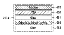
- the touch sensor panel 100 is located between the polarizing layer 282 and the first substrate 281.
- the touch sensor panel 100 is located between the organic material layer 280 and the second substrate 283.
- the touch sensor panel 100 may be positioned between the first substrate 281 and the organic layer 280.
- the first substrate 281 may be made of encapsulation glass
- the second substrate 283 may be made of TFT glass.
- the first substrate 281 and / or the second substrate 283 may be a plastic substrate. Since touch sensing has been described above, only the rest of the configuration will be described briefly.
- the OLED panel is a self-luminous display panel that utilizes the principle that when an electric current is passed through a fluorescent or phosphorescent organic thin film, electrons and holes are combined in the organic layer to generate light, the organic material constituting the light emitting layer is light. Determine the color.
- an OLED utilizes the principle that organic matter emits light when an organic substance is applied onto glass or plastic and electricity is applied. That is, if holes and electrons are injected into the organic anode and cathode, respectively, and recombined with the light emitting layer, excitons having high energy are formed, and the excitons fall into a low energy state. The principle is that light of a specific wavelength is generated while energy is released.
- OLEDs are line-driven PM-OLED (Passive-matrix Organic Light-Emitting Diode) and individual-drive AM-OLED (Active-matrix Organic Light-Emitting-Emitting-Emitting-Emitting-Emitting-Emitting-Emitting-Emitting-Emitting-Emitting-Emitting-Emitting-Emitting-Emitting-Emitting-Emitting-Emitting-Emitting-Emitting). ) Exists. Since both of them do not require a backlight, the display module can be realized very thinly, the light / dark ratio is constant depending on the angle, and the color reproducibility by temperature is good. Undriven pixels are also very economical in that they do not consume power.
- the PM-OLED emits light at a high current only during a scanning time, and the AM-OLED continuously maintains a light emission state at a low current during a frame time. . Therefore, the AM-OLED has the advantages that the resolution is better than that of the PM-OLED, the driving of a large-area display panel is advantageous, and the power consumption is low.
- a thin film transistor (TFT) is incorporated and each element can be individually controlled, it is easy to embody an elaborate screen.
- the OLED (particularly AM-OLED) panel basically includes a polarizing layer 282, a first substrate 281, an organic layer 280, and a second substrate 283.
- the organic layer 280 includes HIL (Hole Injection Layer, hole injection layer), HTL (Hole Transfer Layer, hole transport layer), EIL (Emission Material Layer, electron injection layer), ETL (Electron Transfer Electron, Transport Electron Transport Layer). Layer) and EML (Electron Injection Layer, light emitting layer).
- HIL Hole Injection Layer, hole injection layer
- HTL Hole Transfer Layer, hole transport layer
- EIL emission Material Layer, electron injection layer
- ETL Electron Transfer Electron, Transport Electron Transport Layer
- Layer Electron Transport Electron Transport Layer
- EML Electron Injection Layer, light emitting layer.
- HIL injects holes and uses a substance such as CuPc.
- HTL has a function of moving injected holes, and mainly uses a substance having good hole mobility.
- EIL and ETL are layers for injecting and transporting electrons, and the injected electrons and holes are combined by EML to emit light.
- the EML is composed of a host that determines the lifetime of an organic substance and an impurity that determines color sense and efficiency as materials that embody the color of light emitted. This is merely a description of the basic configuration of the organic layer 280 included in the OLED panel, and the present invention is not limited to the layer structure or material of the organic layer 280.
- the organic layer 280 is inserted between an anode (not shown) and a cathode (not shown). When the TFT is turned on, a driving current is applied to the anode.
- At least a part of the touch sensor is configured to be positioned in the display panel 200A, and at least a remaining part of the touch sensor may be configured to be positioned outside the display panel 200A.
- any one of the drive electrode TX and the reception electrode RX that configure the touch sensor panel 100 may be configured to be located outside the display panel 200A, and the remaining electrodes are disposed inside the display panel 200A. It may be configured to be located.
- an electrode for the operation of the touch sensor may be additionally disposed, but various configurations and / or electrodes positioned inside the display panel 200A may be touch sensing. May be used as a touch sensor. Further, according to the embodiment, at least a part of the touch sensor is configured to be positioned between the first substrate 261 and 281 and the second substrate 261 and 283, and at least the remaining part of the touch sensor is the first. You may comprise so that it may be located in the upper part of 1 board
- the second substrates 262 and 283 may include various layers including a data line, a gate line, a TFT, a common electrode, a pixel electrode, and the like.
- the display panel 200A is an LCD panel
- these electrical components can operate to generate a controlled electric field to align the liquid crystal located in the liquid crystal layer 250.
- Any one of the data line, the gate line, the common electrode, and the pixel electrode included in the second substrates 262 and 283 may be used as a touch sensor.
- the touch input device 1000 including the touch sensor panel 100 that can detect the presence and / or the touch position of the touch has been examined in detail.
- FIG. 3a is a cross-sectional view of an exemplary pressure sensor including a pressure electrode according to an embodiment of the present invention.
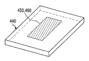
- the pressure sensor 440 may include an electrode layer 441 between the first insulating layer 470 and the second insulating layer 471.
- the electrode layer 441 may include the first electrode 450 and / or the second electrode 460.
- the first insulating layer 470 and the second insulating layer 471 may be an insulating material such as polyimide.
- the first electrode 450 and the second electrode 460 included in the electrode layer 441 may include a material such as copper.
- the electrode layer 441 and the second insulating layer 471 may be bonded with an adhesive (not shown) such as OCA (Optically Clear adhesive).
- the pressure electrodes 450 and 460 spray a conductive spray after positioning a mask having a through hole corresponding to the pressure electrode pattern on the first insulating layer 470. May be formed.
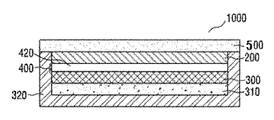
- FIG. 4a is a cross-sectional view of a first example touch input device to which a pressure sensor and a pressure detection module according to an embodiment of the present invention may be applied. The cross-sectional view of the touch input device 1000 illustrated in FIG.
- a touch input device 1000 may be a partial cross-sectional view of the touch input device 1000.
- a touch input device 1000 according to an embodiment of the present invention includes a display panel 200A, a backlight unit 200B disposed at a lower portion of the display panel 200A, and a cover disposed at an upper portion of the display panel 200A.
- the layer 500 may be included.
- the pressure sensors 450 and 460 may be formed on the cover 240.
- the display module 200 may be referred to as including the display panel 200A and the backlight unit 200B.
- the pressure sensors 450 and 460 are attached on the cover 240.
- the pressure sensor 450 and 460 may be included in the touch input device 1000 that performs the same and / or similar functions as the cover 240. It can also be attached to the configuration.
- the touch input device 1000 according to the embodiment of the present invention may be a mobile phone (cell phone), a PDA (Personal Data Assistant), a smartphone (smartphone), a tablet PC (tablet personal computer), an MP3 player, a notebook (notebook), or the like.
- An electronic device including a simple touch screen may be included.
- the display panel 200A may be a display panel in which at least a part of the touch sensor is included in the display panel 200A.
- a driving electrode and a receiving electrode for touch sensing may be included in the display panel 200A.
- the touch sensor panel 100 is not shown separately.
- the touch input device 1000 according to the first example of the present invention may include a touch sensor panel 100 and a display module 200 for detecting a touch position.
- the space may be laminated with an adhesive such as OCA (Optically Clear Adhesive).
- OCA Optically Clear Adhesive
- the cover layer 500 may be formed of a cover glass that protects the front surface of the display panel 200A and forms a touch surface. As illustrated in FIG. 4a, the cover layer 500 may be formed wider than the display panel 200A.
- the display panel 200A such as an LCD panel according to an embodiment of the present invention, cannot emit light by itself, but performs a function of blocking or transmitting light, and thus a backlight unit 200B may be required.
- the backlight unit 200B is positioned below the display panel 200A and includes a light source to illuminate the display panel 200A, so that information having various colors as well as brightness and darkness is displayed on the screen. become.
- the backlight unit 200B may include an optical layer 220 for illuminating the display panel 200A.
- the optical layer 220 will be described in detail with reference to FIG.
- the backlight unit 200B according to the embodiment of the present invention may include a cover 240.
- the cover 240 may be a cover made of metal. When pressure is applied from the outside through the cover layer 500 of the touch input device 1000, the cover layer 500, the display module 200, and the like can be bent.
- the distance between the pressure sensors 450 and 460 and the reference potential layer located inside the display module changes through bending, and a change in capacitance due to such a change in distance is detected via the pressure sensors 450 and 460. By doing so, the magnitude of the pressure can be detected.
- the positions of the pressure sensors 450 and 460 need to be fixed without changing. Accordingly, the cover 240 does not flex relative to the application of pressure, and can serve as a support portion that can fix the pressure sensor.
- the cover 240 may be manufactured separately from the backlight unit 200B and assembled together when the display module is manufactured.
- the display panel 200A and the backlight unit 200B may be configured to include a first air gap 210. This is to protect the display panel 200A and / or the backlight unit 200B from external impacts.
- the first air gap 210 may be configured to be included in the backlight unit 200B.
- the optical layer 220 and the cover 240 included in the backlight unit 200B may be configured to be separated from each other.
- a second air gap 230 may be formed between the optical layer 220 and the cover 240.
- the second air gap 230 may be required to prevent the optical layer 220 and the pressure sensors 450, 460 from contacting and degrading the performance of the optical layer 220.
- the touch input device 1000 may further include support portions 251 and 252 so that the display panel 200A, the backlight unit 200B, and the cover layer 500 can be maintained in a combined state.
- the cover 240 may be formed integrally with the support portions 251 and 252.
- the support portions 251 and 252 can form a part of the backlight unit 200B.
- the structure and function of the LCD panel 200A and the backlight unit 200B are publicly-known technologies and will be briefly described below.
- the backlight unit 200B may include several optical parts.
- FIG. 4B illustrates the optical layer 220 of the backlight unit 200B in the touch input device according to the embodiment.
- FIG. 4B illustrates an optical layer 220 in the case where an LCD panel is used as the display panel 200A. 4b
- the optical layer 220 of the backlight unit 200B may include a reflection sheet 221, a light guide plate 222, a diffusion sheet 223, and a prism sheet 224.
- the backlight unit 200B includes a light source (not shown) disposed on the rear surface and / or the side surface of the light guide plate 222 in the form of a linear light source or a point light source. But you can.
- the light guide plate 222 generally plays a role of converting light from a light source (not shown) in the form of a line light source or a point light source into a surface light source and traveling toward the LCD panel 200A. can do. A part of the light emitted from the light guide plate 222 may be emitted to the opposite side of the LCD panel 200A and lost.
- the reflection sheet 221 may be made of a material having a high reflectivity and located under the light guide plate 222 so that the lost light can be incident on the light guide plate 222 again.
- the diffuser sheet 223 serves to diffuse light incident from the light guide plate 222. For example, since the light scattered by the pattern of the light guide plate 222 directly enters the eyes, the pattern of the light guide plate 222 may be reflected as it is. Furthermore, since such a pattern can be detected with certainty even after the LCD panel 200A is mounted, the diffusion sheet 224 can perform the role of canceling the pattern of the light guide plate 222. After passing through the diffusion sheet 223, the brightness of the light drops abruptly. Accordingly, a prism sheet 224 may be included to improve the brightness of the light by focusing the light again.
- the prism sheet 224 may include a horizontal prism sheet and a vertical prism sheet, for example.
- the backlight unit 200B according to the embodiment of the present invention may include a configuration different from the above-described configuration according to technology changes, developments, and / or embodiments, and may further include an additional configuration other than the above-described configuration.
- the backlight unit 200B according to the embodiment of the present invention includes a protection sheet (protection sheet) as a prism sheet, for example, in order to protect the optical configuration of the backlight unit 200B from external impact or contamination due to inflow of foreign matter.
- An upper portion of 224 may be further included.
- the backlight unit 200B may further include a lamp cover according to an embodiment in order to minimize light loss from the light source.
- the backlight unit 200B can be accurately separated and assembled so that the light guide plate 222, the diffusion sheet 223, the prism sheet 224, the lamp (not shown), etc., which are the main components of the backlight unit 200B, fit the allowable dimensions.
- a frame may be further included so as to maintain the configuration to be performed.
- each of the above-described configurations may consist of two or more separate parts.
- an additional air gap may exist between the light guide plate 222 and the reflection sheet 221. Thereby, the loss light from the light guide plate 222 to the reflection sheet 221 can be incident again on the light guide plate 222 via the reflection sheet 221.
- a double-sided adhesive tape may be included at the end between the light guide plate 222 and the reflection plate 221 so as to maintain the additional air gap.
- DAT Double Adhesive Tape
- the backlight unit 200 ⁇ / b> B and the display module including the backlight unit 200 ⁇ / b> B may include an air gap such as the first air gap 210 and / or the second air gap 230.
- an air gap may be included between a plurality of layers included in the optical layer 220.
- an air gap may be included in the structure also in the case of other display panels.
- FIG. 4c is a cross-sectional view of a second example touch input device to which the pressure sensor and the pressure detection module according to the embodiment of the present invention may be applied.
- FIG. 4 c illustrates a cross section of the touch input device 1000 that further includes the substrate 300 as well as the display module 200.
- the substrate 300 may be mounted with a circuit board and / or a battery for operation of the touch input device 1000 together with a second cover 320 that is an outermost mechanism of the touch input device 1000, for example.
- a housing function that covers the space 310 and the like can be performed.
- a CPU central processing unit
- an AP application processor
- the substrate 300 may be referred to as a mid-frame in the touch input device 1000.
- the cover layer 500 may be formed wider than the display module 200, the substrate 300, and the mounting space 310, so that the second cover 320 is mounted on which the display module 200, the substrate 300, and the circuit board are located.
- the second cover 320 may be formed so as to cover the space 310.
- the pressure sensor 440 may be included between the display module 200 and the substrate 300.
- the touch sensor panel 100 is not shown separately as in FIG. 4A, but the touch input device 1000 according to the embodiment can detect the touch position via the touch sensor panel 100.
- at least a part of the touch sensor may be included in the display panel 200A.
- the pressure sensor 440 may be attached on the substrate 300, may be attached on the display module 200, or may be attached on the display module 200 and the substrate 300. As shown in FIGS.
- the pressure sensor 440 is disposed in the display module 200 or between the display module 200 and the substrate 300 at the bottom of the display module 200.
- the electrodes 450 and 460 included in the pressure sensor 440 may be formed of not only a transparent material but also an opaque material.
- FIGS. 5a to 5e for convenience of explanation, the electrodes 450 and 460 included in the pressure sensor 440 are referred to as pressure sensors.
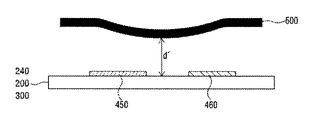
- 5A and 5B illustrate a relative distance between the pressure sensor of the first example included in the touch input device and the reference potential layer and a case where pressure is applied thereto.
- the pressure sensors 450 and 460 may be attached on the cover 240 that can constitute the backlight unit 200B.
- the pressure sensors 450 and 460 and the reference potential layer 600 may be spaced apart by a distance d.
- the reference potential layer 600 and the pressure sensors 450 and 460 may be separated by a spacer layer (not shown). At this time, as described with reference to FIGS.
- the spacer layer may include the first air gap 210, the second air gap 230, and / or the second air gap 230 included in the display module 200 and / or the backlight unit 200B. Or it may be an additional air gap.
- the display module 200 and / or the backlight unit 200A includes one air gap, the one air gap can perform the function of a spacer layer.
- the display module 200 and the backlight unit 200A include a plurality of air gaps, The gap can perform the function of the spacer layer integrally.
- the spacer layer may be positioned between the reference potential layer 600 and the pressure sensors 450 and 460.
- the spacer layer may be implemented with an air gap.
- the spacer layer may be made of a shock absorbing material according to an embodiment.
- the shock absorbing material may include a sponge and a graphite layer.
- the spacer layer may be filled with a dielectric material according to an embodiment. Such a spacer layer may be formed by a combination of an air gap, a shock absorbing material, and a dielectric material.
- the display module 200 can be bent or pressed by a touch applying pressure.
- the display module can be flexed or pressed to show the greatest deformation at the touch location.
- the position showing the largest deformation may not coincide with the touch position, but the display module can show the bending or pressing at least at the touch position.
- the touch position is close to the edge and end of the display module, the position where the display module is most bent or pressed may be different from the touch position.
- the edges or edges of the display module may show little deflection due to touch.
- the display module 200 may be bent or pressed by applying pressure, so that the air gaps 210 and 230 and / or the spacer layer 420 may be maintained.
- the structure (double-sided adhesive tape, adhesive tape 430, support portions 251, 252 and the like) arranged in the above may be made of an inelastic material. That is, the touch pressure can be detected through the bend of the display module 200 or the like even if the structure disposed at the edge to maintain the air gaps 210 and 230 and / or the spacer layer 420 is not compressed or pressed.
- the cover layer 500, the display panel 200A, and / or the backlight unit 200B is bent or pressed when touching the touch input device 1000 according to an embodiment of the present invention, as shown in FIG. As a result, the cover 240 located under the spacer layer may be less bent and pressed.
- the cover 240 is shown as having no deflection or pressure, but this is only an example, and there may be deflection or pressure at the bottom of the cover 240 to which the pressure sensors 450 and 460 are attached.
- the degree can be mitigated through the spacer layer.
- the spacer layer may be implemented with an air gap according to an embodiment of the present invention.
- the spacer layer may be made of a shock absorbing material according to an embodiment.
- the spacer layer may be filled with a dielectric material according to embodiments.
- FIG. 5b illustrates the case where pressure is applied in the structure of FIG. 5a. For example, when an external pressure is applied to the cover layer 500 illustrated in FIG.
- the relative distance between the reference potential layer 600 and the pressure sensors 450 and 460 decreases from d to d ′. . Therefore, in the touch input device 1000 according to the embodiment, when the external pressure is applied, the reference potential layer 600 is configured to bend more than the cover 240 to which the pressure sensors 450 and 460 are attached, thereby enabling the touch pressure. Can be detected. 4A, 5A, and 5B, the case where the first electrode 450 and the second electrode 460 are included as the pressure sensors 450 and 460 for pressure detection is illustrated. At this time, a mutual capacitance may be generated between the first electrode 450 and the second electrode 460.
- one of the first electrode 450 and the second electrode 460 may be a driving electrode, and the remaining one may be a receiving electrode.
- a sensing signal can be acquired through the receiving electrode by applying a driving signal to the driving electrode. If a voltage is applied, a mutual capacitance may be generated between the first electrode 450 and the second electrode 460.
- the reference potential layer 600 may have any potential that can cause a change in the mutual capacitance generated between the first electrode 450 and the second electrode 460.
- the reference potential layer 600 may be a ground layer having a ground potential.
- the reference potential layer 600 may be an arbitrary ground layer included in the display module. According to the embodiment, the reference potential layer 600 may be a ground potential layer that is uniquely included when the touch input device 1000 is manufactured.
- an electrode (not shown) for noise shielding may be included between the first polarizing layer 271 and the first substrate 261.
- the shielding electrode can serve as a ground that can be made of ITO.
- a plurality of common electrodes included in the display panel 200A can form the reference potential layer.
- the potential of the common electrode may be a reference potential.
- the mutual capacitance value between the first electrode 450 and the second electrode 460 may decrease. Since the distance between the reference potential layer 600 and the first electrode 450 and the second electrode 460 is decreased from d to d ′, the fringing capacitance of the mutual capacitance is not only the object but also the reference potential layer 600. It is because it is also absorbed. If the touch object is non-conductive, the change in mutual capacitance can be attributed solely to the change in distance (d-d ') between the reference potential layer 600 and the electrodes 450, 460.
- the pressure sensor 440 includes the first electrode 450 and the second electrode 460 and detects the pressure from the change in mutual capacitance between the two has been described.
- the pressure sensor 440 may be configured to include only one of the first electrode 450 and the second electrode 460 (for example, the first electrode 450).
- 5c and 5d illustrate the relative distance between the pressure sensor of the second example included in the touch input device and the reference potential layer, and the case where pressure is applied thereto. At this time, the magnitude of the touch pressure can be detected by detecting the self capacitance between the first electrode 450 and the reference potential layer 600.
- a drive signal is applied to the first electrode 450 and a change in the self-capacitance between the first electrode 450 and the reference potential layer 600 is detected by receiving a received signal from the first electrode 450.
- the magnitude of the touch pressure can be detected.
- the magnitude of the touch pressure can be detected from a change in capacitance between the first electrode 450 and the reference potential layer 600 caused by a change in distance between the reference potential layer 600 and the first electrode 450. it can. Since the distance d decreases as the touch pressure increases, the capacitance between the reference potential layer 600 and the first electrode 450 may increase as the touch pressure increases.
- the thickness of the first electrode 450 and / or the second electrode 460 is shown to be relatively thick, and these are directly attached to the cover 240.
- the first electrode 450 and / or the second electrode 460 may be attached to the cover 240 as a pressure sensor 440 in the form of an integral sheet. In particular, the thickness may be small.
- the case where the pressure sensor 440 is attached to the cover 240 has been described with reference to the touch input device 1000 illustrated in FIG. 4A. However, the pressure sensor 440 is not included in the touch input device 1000 illustrated in FIG. 4C.
- the display module 200 and the substrate 300 may be disposed.
- the pressure sensor 440 may be attached to the lower part of the display module 200, and in this case, the reference potential layer 600 may be any potential layer located inside the substrate 300 or the display module 200. Further, according to the embodiment, the pressure sensor 440 may be attached to the substrate 300. In this case, the reference potential layer 600 may be the display module 200 or an arbitrary potential layer located inside the display module 200.
- FIG. 5e illustrates the arrangement of the pressure sensor of the third example included in the touch input device. As shown in FIG. 5 e, the first electrode 450 may be disposed on the substrate 300, and the second electrode 460 may be disposed below the display module 200. In this case, another reference potential layer may not be required.
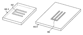
- each of the first electrode 450 and the second electrode 460 may be manufactured to be included in the first pressure sensor 440-1 and the second pressure sensor 440-2 and attached to the touch input device 1000.
- the reference potential layer 600 is located apart from the component to which the pressure sensor 440 is attached in the touch input device 1000 has been described.
- FIG. 6a is a cross-sectional view of a part of the touch input device in which the pressure sensor 440 is attached to the touch input device by the first method.
- the pressure sensor 440 is shown attached on the substrate 300, the display module 200 or the cover 240.
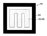
- an adhesive tape 430 having a predetermined thickness may be formed along the edge of the pressure sensor 440 to maintain the spacer layer 420.
- the adhesive tape 430 is shown formed on all edges (eg, four sides of a square) of the pressure sensor 440, but the adhesive tape 430 is at least one of the edges of the pressure sensor 440. It may be formed only on a portion (for example, three sides of a rectangle). At this time, as shown in FIG. 6 b, the adhesive tape 430 may not be formed in the region including the electrodes 450 and 460. Accordingly, when the pressure sensor 440 is attached to the substrate 300 or the display module 200 via the adhesive tape 430, the pressure electrodes 450 and 460 may be separated from the substrate 300 or the display module 200 by a predetermined distance.
- the adhesive tape 430 may be formed on the upper surface of the substrate 300, the lower surface of the display module 200, or the surface of the cover 240.
- the adhesive tape 430 may be a double-sided adhesive tape.
- FIG. 6b only one pressure electrode among the electrodes 450 and 460 is illustrated.
- FIG. 6c is a cross-sectional view of a part of the touch input device in which the pressure sensor is attached to the touch input device by the second method.
- the pressure sensor 440 can be fixed to the substrate 300, the display module 200 or the cover 240 with an adhesive tape 431.
- the adhesive tape 431 can contact at least a part of the pressure sensor 440 and at least a part of the substrate 300, the display module 200, or the cover 240.
- adhesive tape 431 is shown to continue from the top of pressure sensor 440 to the exposed surface of substrate 300, display module 200 or cover 240.
- the adhesive tape 431 may have an adhesive force only on the surface side in contact with the pressure sensor 440. Therefore, in FIG. 6c, the upper surface of the adhesive tape 431 may not have an adhesive force.
- FIG. 6c adhesive tape 431 can contact at least a part of the pressure sensor 440 and at least a part of the substrate 300, the display module 200, or the cover 240.
- adhesive tape 431 is shown to continue from the top of pressure sensor 440 to the exposed surface of substrate 300, display module 200 or cover 240.
- the adhesive tape 431 may have an adhesive force only on the surface side in contact with the pressure sensor 440. Therefore, in FIG. 6c, the upper surface of the adhesive tape 431 may not have an adhesive force.
- the pressure sensor 440 is interposed between the pressure sensor 440 and the substrate 300, the display module 200 or the cover 240.
- Such an air gap in FIG. 6c can also function as a spacer layer 420 for detecting the touch pressure.
- 7A to 7E illustrate pressure electrode patterns included in a pressure sensor for pressure detection according to an embodiment of the present invention.
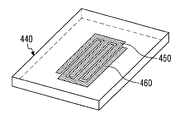
- 7A to 7C illustrate patterns of the first electrode 450 and the second electrode 460 included in the pressure sensor 440.
- FIG. The pressure sensor 440 having the pressure electrode pattern illustrated in FIGS. 7 a to 7 c may be formed on the cover 240, the upper part of the substrate 300, or the lower surface of the display module 200.
- the capacitance between the first electrode 450 and the second electrode 460 may vary depending on the distance between the electrode layer including the first electrode 450 and the second electrode 460 and the reference potential layer 600.
- the magnitude of the touch pressure is detected by changing the mutual capacitance between the first electrode 450 and the second electrode 460, a capacitance range necessary for increasing the detection accuracy is generated.
- the first electrode 450 and the second electrode 460 are formed in the same layer, and the length of the first electrode 450 and the second electrode 460 facing each other is relatively long.
- the case where a pressure electrode is formed is illustrated.
- the pattern of pressure electrodes 450, 460 illustrated in FIGS. 7b-7c may be used to detect pressure on the principle as described in FIGS. 5a and 5c.
- an electrode pattern as illustrated in FIG. 7d may be used.
- the pressure electrode does not need to have a comb shape or a fork shape, which is necessary for improving the detection accuracy of the change amount of the mutual capacitance, and as illustrated in FIG. ) May have a shape.
- an electrode pattern as illustrated in FIG. 7e may be used. At this time, as shown in FIG.
- the first electrode 450 and the second electrode 460 may be disposed so as to be orthogonal to each other to improve the sensing sensitivity of the amount of change in capacitance.
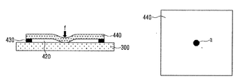
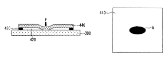
- 8a and 8b show the relationship between the magnitude of the touch pressure and the saturation area in the touch input device to which the pressure sensor 440 according to the present invention is applied.
- 8a and 8b show the case where the pressure sensor 440 is attached to the substrate 300, but the following description applies to the case where the pressure sensor 440 is attached to the display module 200 or the cover 240 as well. obtain.
- the magnitude of the touch pressure is sufficiently large, the distance between the pressure sensor 440 and the substrate 300 may not reach any more at a predetermined position.
- such a state is referred to as a saturated state.
- FIG. 8a when the touch input device 1000 is pressed with a force f, the pressure sensor 440 and the substrate 300 are in contact with each other, and the distance cannot be further approached. At this time, an area where the pressure sensor 440 and the substrate 300 are in contact with each other on the right side of FIG. However, even in such a case, when the magnitude of the touch pressure further increases, the area in a saturated state where the distance between the substrate 300 and the pressure sensor 440 cannot be further approached can be increased. For example, as illustrated in FIG. 8B, if the touch input device 1000 is pressed with a force F greater than the force f, the area where the pressure sensor 440 and the substrate 300 are in contact with each other can be further increased. On the right side of FIG.
- the area where the pressure sensor 440 and the substrate 300 are in contact can be indicated by A. As the area increases, the mutual capacitance between the first electrode 450 and the second electrode 460 may decrease. In the following, it is explained that the magnitude of the touch pressure is calculated based on the change in the capacitance according to the change in the distance. May be included. 8a and 8b will be described with reference to the example shown in FIG. 6a, but the description with reference to FIGS. 8a and 8b will refer to FIGS. 4a, 4c, 5a-5e and 6c. It is obvious that the present invention can be similarly applied to the example described above.
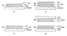
- FIG. 9 illustrates a cross-section of a pressure sensor according to an embodiment of the present invention. Referring to FIG. 9 a, a cross section when a pressure sensor 440 including pressure electrodes 450 and 460 is attached on the substrate 300 or the display module 200 is illustrated.
- the pressure electrodes 450 and 460 are positioned between the first insulating layer 470 and the second insulating layer 471, so that the pressure electrodes 450 and 460 are short-circuited with the substrate 300 or the display module 200. Can be prevented.
- the substrate 300 or the display module 200 to which the pressure electrodes 450 and 460 are attached may not show a ground potential or may show a weak ground potential.
- the touch input device 1000 according to the embodiment of the present invention may further include a ground electrode (not shown) between the substrate 300 or the display module 200 and the insulating layer 470.
- FIGS. 9a to 9d illustrate a partial cross-section in which the pressure sensor according to the embodiment of the present invention is attached to the touch input device.
- the pressure sensor 440 may be configured as illustrated in FIG. 9a. At this time, each of the first electrode 450 and the second electrode 460 shown in FIG.
- first electrode 450 and the second electrode 460 illustrated in FIG. 9A may be configured by electrodes having the form illustrated in FIG. 13B.
- the first electrode 450 and the second electrode 460 may be embodied in different layers according to the embodiment to constitute an electrode layer.
- FIG. 9B illustrates a cross-section when the first electrode 450 and the second electrode 460 are embodied in different layers.
- the first electrode 450 may be formed on the first insulating layer 470
- the second electrode 460 may be formed on the second insulating layer 471 located on the first electrode 450.
- the second electrode 460 may be covered with a third insulating layer 472. That is, the pressure sensor 440 may include the first insulating layer 470 to the third insulating layer 472, the first electrode 450, and the second electrode 460.
- the first electrode 450 and the second electrode 460 may be overlapped with each other.
- the first electrode 450 and the second electrode 460 may be formed to be similar to the pattern of the drive electrode TX and the reception electrode RX arranged in the MXN structure as illustrated in FIG. 13C.
- M and N may be one or more natural numbers.
- the first electrode 450 and the second electrode 460 having a diamond shape may be located in different layers.
- FIG. 9 c illustrates a cross section when the pressure sensor 440 is implemented including only the first electrode 450. As illustrated in FIG.
- the pressure sensor 440 including the first electrode 450 may be disposed on the substrate 300 or the display module 200.
- the first electrode 450 may be arranged as illustrated in FIG. 12d.
- FIG. 9 d shows a cross section when the first pressure sensor 440-1 including the first electrode 450 is attached on the substrate 300 and the second pressure sensor 440-2 including the second electrode 460 is attached to the display module 200.
- the first pressure sensor 440-1 including the first electrode 450 may be disposed on the substrate 300.
- the second pressure sensor 440-2 including the second electrode 460 may be disposed on the lower surface of the display module 200. Similar to that described in connection with FIG.
- the pressure sensor 440 includes a ground electrode (not shown) below the first insulating layers 470, 470-1, and 470-2 disposed so as to be in contact with the substrate 300, the display module 200, or the cover 240. May further be included. At this time, the pressure sensor 440 may further include an additional insulating layer (not shown) positioned to face the first insulating layers 470, 470-1, and 470-2 with a ground electrode (not shown) interposed therebetween. Good.
- the pressure sensor 440 according to the embodiment of the present invention applies pressure to the lower surface of the touch input device 1000.
- the touch pressure can be sensed. 4 to 9, when the pressure sensor 440 according to the present invention is attached to the touch input device, if pressure is applied to the touch input device through the object 500, the display module 200 or the substrate 300 is moved. The magnitude of the touch pressure can be calculated by bending or pressing. At this time, in FIGS. 4 to 9, the display module 200, the substrate 300, or the display module to which pressure is directly applied through the object 500 in order to explain the change in the distance between the reference potential layer 600 and the pressure sensor 440.
- the pressure sensor 440 when the pressure sensor 440 is difficult to maintain the original form, it may be difficult to attach the pressure sensor 440 to the touch input device. Therefore, it is preferable that the pressure sensor 440 has rigidity capable of maintaining the original form.
- the pressure electrodes 450 and 460 included in the pressure sensor 440 are formed of a soft conductive metal such as aluminum (Al), silver (Ag), or copper (Cu), the thickness is low and the thickness thereof is low. Therefore, it is difficult to maintain the original form of the pressure sensor 440 with only the pressure electrodes 450 and 460.
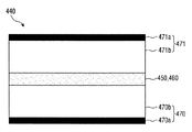
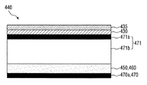
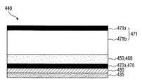
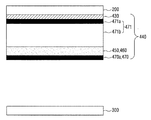
- the pressure sensor 440 may include electrode layers and support layers 470b and 471b.
- the electrode layer may include pressure electrodes 450 and 460 including the first electrode 450 and the second electrode 460.
- the pressure sensor 440 includes a capacitance between the first electrode 450 and the second electrode 460 that is changed by a relative distance change between the reference potential layer 600 and the electrode layer that are spaced apart from the pressure sensor 440.
- the electrode layer may be composed of pressure electrodes 450 and 460 including only one electrode.
- the pressure sensor 440 has a capacitance between the reference potential layer 600 and the reference potential layer 600 that is changed by a relative distance change between the reference potential layer 600 and the electrode layer that are spaced apart from the pressure sensor 440. It may be used to detect changes.
- the reference potential layer 600 that is spaced apart from the pressure sensor 440 cannot have a uniform reference potential depending on the respective input positions, or, for example, a reference potential layer that is spaced apart from the pressure sensor 440.
- the pressure sensor 440 includes a first electrode layer including the first electrode 450 and a second electrode including the second electrode 460 that is spaced apart from the first electrode layer. Layers may be included. In this case, the pressure sensor 440 detects a change in electrostatic capacitance between the first electrode layer and the second electrode layer, which is changed by a relative distance change between the first electrode layer and the second electrode layer.
- any one of the first electrode layer and the second electrode layer may be a reference potential layer.
- a uniform static potential is detected from the reference potential layer located outside the pressure sensor 440 as described above. It can also be applied when a change in capacitance cannot be detected.
- shock absorption and restoring force can be provided between the first electrode layer and the second electrode layer so as to provide uniformity in distance change between the first electrode layer and the second electrode layer.
- the elastic layer 480 may be further included. As shown in FIG.
- the pressure sensor 440 may include a first pressure sensor including a first electrode layer and a first support layer, and a second pressure sensor including a second electrode layer and a second support layer. Good. In this case, the pressure sensor 440 detects a change in electrostatic capacitance between the first electrode layer and the second electrode layer, which is changed by a relative distance change between the first electrode layer and the second electrode layer. Can be used.
- the support layers 470b and 471b have a rigidity capable of maintaining the form of the pressure sensor 440 even when a relative distance change from the reference potential layer 600 of the pressure sensor 440 such as a resin material, a highly rigid metal, or paper occurs. It may be formed of an attribute material.
- the pressure sensor 440 may further include a first insulating layer 470 and a second insulating layer 471.
- the electrode layer is positioned between the first insulating layer 470 and the second insulating layer 471, and the support layers 470 b and 471 b are disposed on at least one of the first insulating layer 470 and the second insulating layer 472. May be included.
- the first insulating layer 470 or the second insulating layer 472 may further include electrode cover layers 470a and 471a.
- the electrode cover layers 470a and 471a can function to protect the electrode layer, such as the function of insulating the electrode layer and the prevention of oxidation, scratching, cracking, and the like of the electrode.
- the electrode cover layers 470a and 471a may be formed or coated with a material containing color, and may prevent the pressure sensor 440 from being deteriorated by being exposed to light when the pressure sensor 440 is distributed. .
- the electrode cover layers 470a and 471a may be bonded to the electrode layers or support layers 470b and 471b with an adhesive, but may be printed or coated.
- the electrode cover layers 470a and 471a may also be formed of a resin material having high rigidity, but since the thickness is only a few ⁇ m, it is difficult to maintain the pressure sensor 440 of about 100 ⁇ m in its original form. As shown in FIGS.
- the pressure sensor 440 may further include an adhesive layer 430 and a protective layer 435 outside the first insulating layer 470 or the second insulating layer 471.
- the adhesive layer 430 is configured separately from the pressure sensor 440.
- the adhesive layer 430 may be included in the pressure sensor 440 and manufactured as one configuration.
- the protective layer 435 functions to protect the adhesive layer 430 before the pressure sensor 440 is attached to the touch input device. When the pressure sensor 440 is attached to the touch input device, the protective layer 435 is removed to remove the adhesive layer.
- the pressure sensor 440 can be attached to the touch input device using 430. As shown in FIG.
- the electrode cover layers 470a and 471a may not be formed on the side where the support layers 470b and 471b are formed.
- the support layers 470b and 471b are formed of a resin material or paper, the electrode layers can be insulated and protected.
- the support layers 470b and 471b may also be formed or coated with a material including color.
- the thickness of either the first insulating layer 470 or the second insulating layer 471 may be smaller than the other thickness.
- the capacitance C is inversely proportional to the distance d between the electrode layer and the reference potential layer 600, as shown in FIG. 3i, the electrode layer and the reference potential layer with respect to the same distance change.
- the pressure sensor 440 is attached to the touch input device including the cover 240, the substrate 300, and / or the display module 200, but is positioned near the reference potential layer 600 in the first insulating layer 470 or the second insulating layer 471.
- the thickness of the insulating layer may be smaller than the thickness of the insulating layer located far from the reference potential layer 600.
- only one of the first insulating layer 470 and the second insulating layer 471 may include the support layers 470b and 471b.
- the support layers 470b and 471b are formed only on the insulating layer located far from the reference potential layer 600 among the first insulating layer 470 and the second insulating layer 471. May be included. Similarly, as shown in FIG.
- the pressure sensor 440 when the pressure sensor 440 includes a first electrode layer including the first electrode 450 and a second electrode layer including the second electrode 460 that is spaced apart from the first electrode layer,
- the thickness of either the first insulating layer 470 or the second insulating layer 471 may be smaller than the other thickness.
- the pressure sensor 440 when the pressure sensor 440 is attached to the display module 200 or the substrate 300, if pressure is applied to the touch input device, the distance between the pressure sensor 440 and the member to which the pressure sensor 440 is attached does not change. The distance between the pressure sensor 440 and the member to which the pressure sensor 440 is not attached changes.
- the pressure sensor 440 is attached to the touch input device including the substrate 300 and the display module 200, but the substrate 300 and the display module 200 are attached to one of the one surface of the substrate 300 and the one surface of the display module 200, In a state where the pressure sensor 440 is attached to the touch input device, the thickness of the insulating layer located at a position close to one surface of the first insulating layer 470 or the second insulating layer 471 to which the pressure sensor 440 is attached is equal to the pressure sensor.
- first insulating layer 470 and the second insulating layer 471 may include the support layers 470b and 471b.
- the support layers 470b and 471b may be included.
- FIG. 3e is attached to the cover 240, the substrate 300 or the display module 200 on the side where the adhesive layer 430 is formed, and the reference potential layer 600 formed on the member side where the pressure sensor 440 is not attached.
- FIG. 3F illustrates a pressure sensor 440 used for detecting the magnitude of pressure by changing a distance between the electrode layer and the cover 240 on the side where the adhesive layer 430 is formed. Pressure attached to the substrate 300 or the display module 200 and used for detecting the magnitude of the pressure by changing the distance between the reference potential layer 600 formed on the member side to which the pressure sensor 440 is attached and the electrode layer. Sensor 440.
- the space in which the pressure sensor 440 is disposed for example, the interval between the display module 200 and the substrate 300 differs depending on the touch input device, but is about 100 to 500 ⁇ m, so that the pressure sensor 440 and the support layers 470b and 471b
- the thickness is limited. As shown in FIG. 3g, when the pressure sensor 440 is attached to the display module 200 and the distance between the display module 200 and the substrate 300 is 500 ⁇ m, the thickness of the pressure sensor 440 is between 50 ⁇ m and 450 ⁇ m. It should have a value. If the thickness of the pressure sensor 440 is smaller than 50 ⁇ m, the thicknesses of the support layers 470b and 471b having relatively high rigidity are also reduced.
- the pressure sensor 440 it is difficult for the pressure sensor 440 to maintain the original form. If the thickness of the pressure sensor 440 is larger than 450 ⁇ m, the distance between the pressure sensor 440 and the substrate 300 that is the reference potential layer is relatively small when the thickness is 50 ⁇ m or less, so that it is difficult to measure a wide range of pressures. . Since the pressure sensor 440 is disposed in the touch input device, it must satisfy the reliability given under predetermined conditions such as temperature and humidity as in the touch input device.
- the support layers 470b and 471b are preferably resin materials in order to satisfy the reliability with little change in appearance and characteristics under severe conditions of 85 degrees Celsius to -40 degrees Celsius and humidity conditions of 85%.
- the support layers 470b and 471b may be formed of polyimide (PI) or polyethylene terephthalate (PET). Also, when polyethylene terephthalate is used, costs can be saved over polyimide. The material forming the support layers 470b and 471b can be determined in consideration of reliability as well as cost. As described in detail above, in order to detect the pressure via the touch input device 1000 to which the pressure sensor 440 according to the embodiment of the present invention is applied, a change in capacitance generated in the pressure electrodes 450 and 460 is detected. Need to sense.
- PI polyimide
- PET polyethylene terephthalate
- a drive signal needs to be applied to the drive electrode of the first electrode 450 and the second electrode 460, and the touch pressure cannot be calculated from the change in capacitance by obtaining a sensing signal from the reception electrode. Don't be.
- a pressure sensing device may additionally be included in the form of a pressure sensing IC for pressure sensing operations.
- the pressure detection module (not shown) according to the embodiment of the present invention may be configured to include not only the pressure sensor 440 for pressure detection but also such a pressure detection device. In such a case, as illustrated in FIG. 1, since the configuration similar to the driving unit 120, the sensing unit 110, and the control unit 130 is included, the area and volume of the touch input device 1000 are increased. Problems can arise.
- the touch input device 1000 applies a driving signal for pressure detection to the pressure sensor 440 using a touch detection device for operating the touch sensor panel 100, and receives a sensing signal from the pressure sensor 440.
- the touch pressure can also be detected.
- the first electrode 450 is a drive electrode and the second electrode 460 is a reception electrode.
- the first electrode 450 receives a driving signal from the driving unit 120, and the second electrode 460 receives the sensing signal. Can be communicated to.
- the controller 130 may scan the touch sensor panel 100 and perform pressure detection scanning, or the controller 130 may perform time-division scanning of the touch sensor panel 100 during the first time interval.
- the control signal can be generated so as to perform scanning for pressure detection in a second time period different from the first time period. Therefore, in the embodiment of the present invention, the first electrode 450 and the second electrode 460 must be electrically connected to the driving unit 120 and / or the sensing unit 110.
- the touch detection device for the touch sensor panel 100 is generally formed as one end of the touch sensor panel 100 as the touch sensing IC 150 or on the same plane as the touch sensor panel 100.
- the pressure electrodes 450 and 460 included in the pressure sensor 440 may be electrically connected to the touch detection device of the touch sensor panel 100 by any method.
- the pressure electrodes 450 and 460 may be connected to the touch detection device through a connector using the second PCB 210 included in the display module 200.
- the conductive traces 461 that respectively extend from the first electrode 450 and the second electrode 460 may be electrically connected to the touch sensing IC 150 via the second PCB 210 or the like.
- 10a and 10b show a case where a pressure sensor 440 including pressure electrodes 450 and 460 is attached to the lower surface of the display module 200.
- the display module 200 includes a second PCB 210 on which a circuit for operating the display panel is mounted on a part of a lower surface.
- FIG. 10 a illustrates a case where the pressure sensor 440 is attached to the lower surface of the display module 200 such that the first electrode 450 and the second electrode 460 are connected to one end of the second PCB 210 of the display module 200.
- the first electrode 450 and the second electrode 460 may be connected to one end of the second PCB 210 using a double-sided conductive tape.
- the first is made using a double-sided conductive tape rather than using another connector. It is more effective to connect the electrode 450 and the second electrode 460 to one end of the second PCB 210 because the thickness can be reduced.
- a conductive pattern may be printed on the second PCB 210 so that the pressure electrodes 450 and 460 can be electrically connected to a necessary configuration such as the touch sensing IC 150. A detailed description thereof will be described with reference to FIGS. 11a to 11c.
- FIG. 10 a may be similarly applied to the substrate 300 and the cover 240.
- FIG. 10b illustrates a case where the pressure sensor 440 including the first electrode 450 and the second electrode 460 is not separately manufactured and is integrally formed on the second PCB 210 of the display module 200.
- the second PCB 210 of the display module 200 is manufactured, not only a circuit for operating the display panel in advance but also a pattern corresponding to the first electrode 450 and the second electrode 460 by omitting a certain area 211 from the second PCB. Can be printed.
- the second PCB 210 may be printed with a conductive pattern that electrically connects the first electrode 450 and the second electrode 460 to a necessary configuration such as the touch sensing IC 150.
- 11a to 11c illustrate a method of connecting the pressure electrodes 450 and 460 included in the pressure sensor 440 to the touch sensing IC 150.
- FIG. In FIGS. 11a to 11c when the touch sensor panel 100 is included outside the display module 200, the touch detection device of the touch sensor panel 100 is mounted on the touch sensing IC 150 mounted on the first PCB 160 for the touch sensor panel 100. The case where it accumulates is illustrated.
- 11A illustrates a case where the pressure electrodes 450 and 460 included in the pressure sensor 440 attached to the display module 200 are connected to the touch sensing IC 150 through the first connector 121.
- the touch sensing IC 150 is connected to the second PCB 210 for the display module 200 through the first connector 121.
- the second PCB 210 may be electrically connected to the main board via the second connector 224. Accordingly, the touch sensing IC 150 can exchange signals with the CPU or AP for operating the touch input device 1000 via the first connector 121 and the second connector 224.
- the pressure sensor 440 is attached to the display module 200 in the manner illustrated in FIG. 10b, but is attached in the manner illustrated in FIG. 10a. It may also be applied to cases.
- a conductive pattern may be printed on the second PCB 210 so that the pressure electrodes 450 and 460 can be electrically connected to the touch sensing IC 150 via the first connector 121.
- FIG. 11 b illustrates a case where the pressure electrodes 450 and 460 included in the pressure sensor 440 attached to the display module 200 are connected to the touch sensing IC 150 through the third connector 473.
- the pressure electrodes 450 and 460 are connected to the main board for the operation of the touch input device 1000 through the third connector 473, and then the touch sensing IC 150 through the second connector 224 and the first connector 121. May be connected.
- the pressure electrodes 450 and 460 may be printed on an additional PCB separated from the second PCB 210.
- the pressure electrodes 450 and 460 are attached to the touch input device 1000 in the form of the pressure sensor 440 as illustrated in FIGS. 3a to 3h, and the conductive traces and the like are extended from the pressure electrodes 450 and 460.
- the main board may be connected via the connector (473).
- FIG. 11c illustrates a case where the pressure electrodes 450 and 460 are directly connected to the touch sensing IC 150 via the fourth connector 474.
- the pressure electrodes 450, 460 may be connected to the first PCB 160 via the fourth connector 474.
- the first PCB 160 may be printed with a conductive pattern that is electrically connected from the fourth connector 474 to the touch sensing IC 150.
- the pressure electrodes 450 and 460 may be connected to the touch sensing IC 150 via the fourth connector 474.
- the pressure electrodes 450 and 460 may be printed on an additional PCB separated from the second PCB 210.
- the second PCB 210 and the additional PCB may be insulated so as not to short-circuit each other.
- the pressure electrodes 450 and 460 are attached to the touch input device 1000 in the form of the pressure sensor 440 as illustrated in FIGS. 3a to 3h, and the conductive traces and the like are extended from the pressure electrodes 450 and 460.
- the first PCB 160 may be connected through the connector 474.
- the touch sensing IC 150 is described on the assumption of a COF (chip on film) structure in which the first PCB 160 is formed. However, this is merely an example, and the present invention may be applied to a case where the touch sensing IC 150 has a COB (chip on board) structure in which the touch sensing IC 150 is mounted on the main board in the mounting space 310 of the touch input device 1000. Good. From the description with respect to FIGS.
- the pressure electrodes 450, 460 are connected via connectors in other embodiments.
- the first electrode 450 as one drive electrode constitutes one channel
- the second electrode 460 as a reception electrode constitutes one channel.
- the driving electrode and the receiving electrode may each form a plurality of channels according to the embodiment.
- the driving electrode and the receiving electrode constitute a plurality of channels, it is possible to improve the accuracy when detecting the pressure for the touch, and it is possible to detect the multiple pressures for the multi touch. It can be.
- 12a to 12d illustrate the case where the pressure electrode of the present invention forms a plurality of channels. In FIG.
- FIG. 12a illustrates an example in which the first electrodes 450-1 and 450-2 and the second electrodes 460-1 and 460-2 constituting two channels are all included in one pressure sensor 440.
- the first electrode 450 constitutes two channels 450-1 and 450-2
- the second electrode 460 constitutes one channel
- FIG. 12c illustrates a case where each of the first electrodes 450-1 to 450-5 and the second electrodes 460-1 to 460-5 constitutes five channels. In this case as well, the electrodes constituting the five channels may all be included in one pressure sensor 440.
- FIG. 12a illustrates an example in which the first electrodes 450-1 and 450-2 and the second electrodes 460-1 and 460-2 constituting two channels are all included in one pressure sensor 440.
- the first electrode 450 constitutes two channels 450-1 and 450-2
- the second electrode 460 constitutes one channel.
- FIG. 12c illustrates a case where each of the first electrodes 450-1 to 450-5 and the second electrodes 460
- each of the first electrodes 451 to 459 constitutes nine channels and is included in one pressure sensor 440 is illustrated.
- the first electrodes 450 and / or the second electrodes 460 are electrically connected to the touch sensing IC 150.
- a conductive pattern may be formed.
- a case where a plurality of channels of the form shown in FIG. 12d are configured will be described as an example.
- the plurality of conductive patterns 461 must be connected to the first connector 121 having a limited width, the width of the conductive pattern 461 and the interval between the adjacent conductive patterns 461 must be small.
- polyimide is more suitable than polyethylene terephthalate.
- the support layers 470b and 471b of the pressure sensor 440 on which the conductive pattern 461 is formed may be formed of polyimide.
- a soldering process may be required to connect the conductive pattern 461 to the first connector 121.
- it is more difficult than polyethylene terephthalate which is relatively heat-sensitive. Suitable for heat-resistant polyimide.
- FIGS. 12a to 12d and FIGS. 13a to 13d exemplify the case where the pressure electrode constitutes a single channel or a plurality of channels, and the pressure electrode may be composed of a single channel or a plurality of channels by various methods. 12A to 12C and FIGS. 13A to 13D, the case where the pressure electrodes 450 and 460 are electrically connected to the touch sensing IC 150 is not illustrated. However, the pressure electrode 450 is not illustrated in FIGS.
- the first connector 121 or the fourth connector 474 may be a double-sided conductive tape. Specifically, since the first connector 121 or the fourth connector 474 is disposed at a very small interval, it is possible to reduce the thickness by using double-sided conductive tape rather than using another connector. So it is effective.
- the function of the first connector 121 or the fourth connector 474 may be implemented through a FOF bonding (Flex-on-Flex Bonding) method capable of realizing a thin thickness.
- FIG. 20a is a flowchart for explaining an example of a method for detecting the magnitude of touch pressure using a plurality of channels in the touch input device according to the embodiment of the present invention. If pressure is applied to the touch surface (S10), the touch pressure is based on the sum of values obtained by multiplying the change in capacitance detected in each channel and the SNR improvement scaling factor assigned to each channel. Is detected (S20). For example, in the pressure sensor 440 shown in FIG.
- Second method example 14A is a diagram illustrating a case where pressure is applied to a predetermined position in the pressure sensor illustrated in FIG. 13D, and FIG.
- FIG. 14B is a diagram in which touch pressure is applied to the touch surface corresponding to position A in FIG. 14A.
- FIG. 14C is a cross-sectional view illustrating a form in which the touch input device is bent when touch pressure is applied to the touch surface corresponding to the position C in FIG. 14A.
- FIG. When touch pressure is applied to the touch surface corresponding to the A position shown in FIG. 14a, that is, when touch pressure is applied to the center portion of the display module 200, as shown in FIG. The degree to which the module 200 bends is relatively large.
- touch pressure is applied to the touch surface corresponding to the B position shown in FIG. 14a, that is, when touch pressure is applied to the edge of the display module 200, as shown in FIG.
- the display module 200 It is relatively smaller than the degree to which the display module 200 bends. Specifically, as shown in FIGS. 14b and 14c, when the same touch pressure is applied, the position where the display module 200 bends most when the touch pressure is applied to the center of the display module 200.
- the distance d1 between the pressure electrode 450 and the pressure electrode 450 is smaller than the distance d2 between the pressure electrode 450 and the position where the display module 200 bends most when the touch pressure is applied to the end of the display module 200. Therefore, even if the same touch pressure is applied, the amount of change in capacitance detected in each channel differs depending on the position where the touch pressure is applied.
- FIG. 20B is a flowchart for explaining another example of a method of detecting the magnitude of the touch pressure using a plurality of channels in the touch input device according to the embodiment of the present invention.
- 13d is a diagram illustrating sensitivity correction scaling factors assigned to the first electrodes in the pressure sensor illustrated in FIG. 13d.
- the first electrode 450 positioned at the center of the display module 200 is assigned 1 as a sensitivity correction scaling factor, and the first electrode 450 adjacent to the first electrode 450 positioned at the center is used.
- One electrode 450 may be assigned 6 as a sensitivity correction scaling factor, and the first electrode 450 located further on the edge may be assigned 12 and 16 as sensitivity correction scaling factors.
- FIG. 14 c when the same pressure is applied, the capacitance detected at the central portion of the display module 200 due to the central portion of the display module 200 being bent more than the end of the display module 200. It can be offset that the amount of change of becomes larger than the amount of change of capacitance detected at the end of the display module 200. Therefore, a slightly more accurate pressure value can be calculated.
- FIG. 16A is a graph for explaining the relationship between the magnitude of the applied pressure and the volume change amount of the touch input device when pressure is applied to the position shown in FIG. 14A.
- FIG. FIG. 16C is a cross-sectional view illustrating the volume change amount of the touch input device illustrated in FIG. 14C.
- FIG. 16C is a cross-sectional view illustrating the volume change amount of the touch input device illustrated in FIG.
- volume change amount the volume of the touch input device 1000 when the touch pressure is applied to the central portion of the display module 200 (hereinafter referred to as volume change amount) touches the end of the display module 200. This is larger than the volume change amount of the touch input device 1000 when the pressure is applied.
- the display module The volume change amount of the touch input device 1000 when the touch pressure is applied to the A position, which is the center of the 200, is applied to the C position, which is located at the end relative to the A position of the display module 200. It is larger than the volume change amount of the touch input device 1000 at the time. At this time, when the touch pressure is applied to the same position, the magnitude of the applied pressure and the volume change amount of the touch input device 1000 have a linear relationship. That is, when comparing the case where a different pressure is applied to any one of the A, B, and C positions shown in FIG.
- the volume change amount of the touch input device 1000 changes in proportion to the magnitude of the applied pressure. Therefore, by estimating the volume change amount of the touch input device 1000, the magnitude of the pressure can be detected.
- a reference value corresponding to the touch position is stored in a memory (not shown) based on the capacitance detected from each channel. ).
- the reference value may be a volume change amount of the touch input device 1000 calculated based on a capacitance detected from each channel.
- the reference value may be a normalized pressure value having a linear relationship with the volume change amount of the touch input device 1000, or a slope in the graph shown in FIG.
- Such a method is repeatedly executed for each touch position, and reference values for all positions in the entire area of the display module 200 when a predetermined amount of pressure is applied are stored in the memory.
- the reference values are generated and stored only for a plurality of representative positions separated by a predetermined interval.
- the calculated 432 is based on the detected amount of change in capacitance. Individual volume changes can be stored in the memory.
- FIG. 20c is a flowchart for explaining another example of a method of detecting the magnitude of the pressure of the touch using a plurality of channels in the touch input device according to the embodiment of the present invention.
- FIG. 17 is a partial perspective view for explaining a form in which the touch input device is deformed when a pressure is applied to the touch input device, and FIG. 17B illustrates a volume of the touch input device when a pressure is applied to the touch input device.
- FIG. 17c is a diagram for explaining the estimation of the amount of change, and FIG. 17c is a cross-sectional view of the drawing shown in FIG. 17b.
- the touch position is detected (S2000), and the change in distance corresponding to each channel is calculated from the amount of change in capacitance detected in each channel (S3000).
- the capacitance value detected in each channel differs depending on the configuration of the pressure electrode and the circuit configuration for sensing the touch pressure, but corresponds to each channel shown in FIG. 17c when the touch pressure is applied. Since it may be expressed as a function of the distance change di, it is possible to calculate the distance change di corresponding to each channel by calculating backward from the capacitance value detected from each channel.
- the distance change di corresponding to each channel means a distance by which the surface of the touch input device corresponding to each channel is deformed after the pressure is applied with reference to before the pressure is applied.
- the first electrode 450 is the drive electrode TX
- the second electrode 460 is the reception electrode RX
- the first electrode 450 and the second electrode 460 are separated.
- An example of an equivalent circuit of a device that senses the pressure capacitance 11 between the first electrode 450 and the second electrode 460 when detecting the magnitude of the touch pressure from the change in mutual capacitance between them is illustrated.
- the relational expression between the drive signal Vs and the output signal Vo can be expressed as Expression (1).
- the pressure capacitance 11 can be expressed as follows.
- Co is a fixed capacitance value generated between the first electrode 450 and the second electrode 460
- Equation (2) can be expressed as C fringing
- the value is expressed by a distance d and a coefficient ⁇ .
- the fixed capacitance means a capacitance generated by the first electrode 450 and the second electrode 460 regardless of the distance d from the reference potential layer.
- FIG. 18B is configured such that a driving signal is applied to the first electrode 450 and a received signal is detected from the first electrode 450 as shown in FIG.
- An example of an equivalent circuit of a device that senses the capacitance 11 between the first electrode 450 and the reference potential layer when detecting the magnitude of the touch pressure from the change in the voltage is illustrated.
- the third switch 23 is turned on, the charge charged in the pressure capacitor 11 is transmitted to the amplifier 31 and the corresponding output signal Vo can be obtained. . If the second switch 22 is turned on, all charges remaining in the pressure capacitor 11 are discharged, and if the third switch 23 is turned on immediately after the second switch 22 is turned off, the feedback capacitor 32 is passed through. Charge is transferred to the pressure capacitor 11 and an output signal corresponding to the charge can be obtained. At this time, the output signal Vo of the circuit displayed in FIG. 18B can be expressed as Equation (3).
- ⁇ is the dielectric constant ⁇ o ⁇ r of the material filled between the first electrode 450 and the reference potential layer
- A is the area of the first electrode 450.
- the volume change amount of the touch input device is estimated using the calculated distance change di corresponding to each channel (S4000). Specifically, when a touch pressure is applied, the surface of the touch input device 1000 is deformed as shown in FIG. 17A, and the volume change amount of the touch input device 1000 is shown in FIGS. 17B and 17C. It can be estimated by the total volume change corresponding to each channel. At this time, if the area corresponding to each channel is the same, for example, if the area of each first electrode 450 shown in FIG.
- the total volume change amount corresponding to each channel is It may be a value obtained by multiplying the sum of the corresponding distance changes di by the area A of one first electrode 450.
- the magnitude of the applied pressure and the volume change amount of the touch input device 1000 have a linear relationship as shown in FIG.
- the magnitude of the applied pressure is calculated (S5000). .
- the estimated volume change amount of the touch input device 1000 is 1000, and the reference value corresponding to the corresponding touch position with respect to the pressure of 800 g is used as the reference value.
- the volume change amount stored in the memory is 2000
- the applied pressure is 400 g.
- various methods such as linear interpolation and bi-cubic interpolation are used by using the reference value corresponding to the adjacent touch position stored in the memory.
- the pressure value can be calculated through interpolation.
- 19A is a view for explaining a case where pressure is applied to the D position of the pressure sensor shown in FIG. 14A, and FIG.
- 19B is a case where pressure is applied to the D position shown in FIG. 19A. It is a graph for demonstrating calculating a pressure value.
- the reference values corresponding to the A position and the B position shown in FIG. 19a are stored in the memory, but the reference value corresponding to the D position which is an intermediate point between the A position and the B position is stored in the memory.
- the reference value for the D position is obtained by linearly interpolating the reference values for the A position and the B position, that is, taking the intermediate value between the reference value for the A position and the reference value for the B position.
- the magnitude of the pressure applied to the D position can be calculated using the estimated reference value of the D position.
- FIG. 21a is a graph showing the magnitude of a signal including information on the capacitance detected in the channel corresponding to the position a in FIG. 17c, and FIG. 21b is detected in the channel corresponding to the position b in FIG. 17c. It is a graph which shows the magnitude
- the magnitude of the signal including information on the capacitance detected in the channel corresponding to the position a is the position b. Greater than the magnitude of the signal containing information on the capacitance detected in the corresponding channel.
- the capacitance detected in each channel varies depending not only on the pressure applied to the touch input device 1000 but also on various factors such as a change in electric field or magnetic field around the touch input device 1000 and a change in temperature. obtain. Such a change in capacitance due to factors other than the pressure applied to the touch input device 1000 corresponds to noise that must be removed when detecting the magnitude of the pressure. As shown in FIGS.
- a signal including information on capacitance detected in each channel is detected in a form in which a signal caused by applied pressure and a signal caused by noise are combined. Is done.
- the specific gravity occupied by the magnitude of the signal due to the pressure is While the specific gravity occupied by the signal due to noise is larger than the specific gravity, as shown in FIG. 21b, among the signals detected at the position b corresponding to the end of the display module far from the position where the pressure is applied, The specific gravity occupied by the size of the signal due to the noise is relatively smaller than the specific gravity occupied by the signal due to the noise.
- the signal due to noise is generally constant regardless of the position where the pressure is applied, so the magnitude of the signal due to noise detected in each channel is generally constant, but due to pressure. Since the signal varies depending on the position where the pressure is applied, the signal resulting from the pressure detected in each channel varies depending on the position where the pressure is applied. Therefore, if the signal detected in the channel whose signal due to noise is relatively larger than the signal due to pressure is eliminated when detecting the magnitude of pressure or the contribution is reduced, In particular, since the degree to which the signal due to noise decreases is greater than the degree to which the signal due to pressure decreases, the overall SNR can be improved. Specifically, by assigning an appropriate SNR improvement scaling factor to each channel, the overall SBR can be improved during pressure detection.
- the position where the pressure is applied does not necessarily coincide with the position where the display module exhibits the largest deformation.
- the magnitude of the signal including information on the capacitance detected in the channel corresponding to the position where the voltage is applied is approximately larger than the magnitude of the signal including information on the capacitance detected in the channel corresponding to the other position. large. Accordingly, the SNR improvement scaling factor assigned to each channel can be calculated according to the magnitude of the signal including information on the position where the pressure is applied, i.e., the touch position or the capacitance detected in each channel.
- FIG. 22a and 22b are diagrams for explaining an SNR improvement scaling factor assigned to each channel when pressure is applied to the P position
- FIG. 22c is a view illustrating pressure applied to the P position of FIG. 22a
- 6 is a diagram showing the amount of change in capacitance detected in each channel when the operation is performed.
- the SNR is improved by detecting the pressure using only a part of the entire channel where the magnitude of the detected signal is large and by eliminating the channel having the small signal when detecting the pressure. Can be made.
- N is greater than 1 or equal to or less than the total number of channels or the same natural number. Specifically, when pressure is applied to the P position in FIG. 22a and N is 4, CH2, CH4, CH5, which are the channels from which the four largest signals are detected, as shown in FIG. 22c, and CH8 is assigned 1 as the SNR improvement scaling factor, and the remaining channels are assigned 0 as the SNR improvement scaling factor.
- the pressure is calculated using 310 which is the total of the change amounts of the capacitance detected in CH2, CH4, CH5, and CH8.
- the size can be detected.
- 1 is assigned as the SNR improvement scaling factor to the channel in which a signal having a magnitude equal to or greater than a predetermined ratio of the largest signal is detected, and the remaining channels are assigned.
- 0 can be assigned as the SNR improvement scaling factor to be applied.
- SNR can be improved.
- the signal output from CH5, which is the channel in which the largest signal is detected. 1 is assigned as an SNR improvement scaling factor to CH4, CH5, and CH8, which are channels in which a signal having a magnitude of 55 or more, which is 50% of the signal size, is detected, and 0 is assigned as an SNR improvement scaling factor to the remaining channels. It is done.
- the SNR improvement scaling factor is applied to the first method example described above, the magnitude of the pressure is calculated using 260 which is the sum of the change amounts of the capacitance detected in CH4, CH5, and CH8. Can be detected.
- N is greater than 1 or equal to or less than the total number of channels or the same natural number. Specifically, when pressure is applied to the P position of FIG.
- the four channels closest to the touch position, CH4, CH5, CH7, and CH8, are applied. 1 is assigned as the SNR improvement scaling factor, and 0 is assigned to the remaining channels as the SNR improvement scaling factor.
- the SNR improvement scaling factor is applied to the first method example described above, the pressure is calculated using 305 which is the total amount of change in capacitance detected by CH4, CH5, CH7 and CH8. The size can be detected. Also, it is possible to assign 1 as an SNR improvement scaling factor to a channel located within a predetermined distance from the touch position and assign 0 as an SNR improvement scaling factor to the remaining channels.
- the SNR improvement scaling coefficient is applied to the first method example described above, it is the sum of the amount of change in capacitance detected in CH1, CH2, CH4, CH5, CH6, CH7 and CH8. 385 can be used to detect the magnitude of the pressure. Also, based on the distance between the touch position and each channel, the SNR improvement scaling factor assigned to each channel can be calculated. In one embodiment, the distance between the touch location and each channel and the SNR improvement scaling factor assigned to each channel may have an inversely proportional relationship. At this time, the SNR can be improved by reducing the degree of contribution to the pressure detection of the channel having a small signal size among the entire channels. Specifically, when a touch is input at the P position in FIG.
- an SNR improvement scaling factor proportional to 1 / dj can be assigned to the channel j.
- d1 to d15 shown in FIG. 22b are 15, 13.5, 13.3, 11.3, 9.3, 8.8, 8.5, 5.3, 4.5, 7. If it has a value of 3, 3.3, 1, 8.5, 5.3, 4.5, 1 / dj is 0.067, 0.074, 0.075, 0.088, 0.108, 0.114, 0.118, 0.189, 0.122, 0.137, 0.303, 1, 0.118, 0.189, 0.222 are assigned as SNR improvement scaling factors for CH1 to CH15, respectively. It is done.
- the SNR improvement scaling factor is applied to the first example method described above, the sum of values obtained by multiplying the capacitance change amount detected in each channel by the SNR improvement scaling factor is used. The size can be detected.
- the example in which the SNR improvement scaling factor is applied to the first method example described above has been described.
- the SNR scaling factor is similarly applied to the second method example or the third method example to apply pressure. Can be detected.
- the pressure sensor 440 of the form shown in FIG. 13d has been described.
- the present invention is not limited to this, and can be applied to a pressure sensor including the pressure electrode of the form shown in FIGS. 13a to 13c.
- multiple pressure detection for multiple touches may be possible. This may be performed using, for example, the magnitude of pressure acquired from the channels of the pressure electrodes 450 and 460 disposed at positions corresponding to the multiple touch positions acquired from the touch sensor panel 100.
- the pressure position can be directly detected by the pressure sensor 440, and the channels of the pressure electrodes 450 and 460 disposed at the corresponding positions. Multiple pressure detections can be performed using the pressure magnitude obtained from.
- the embodiment has been mainly described. However, this is merely an example, and does not limit the present invention. Any person having ordinary knowledge in the field to which the present invention belongs will be described.
Landscapes
- Engineering & Computer Science (AREA)
- General Engineering & Computer Science (AREA)
- Theoretical Computer Science (AREA)
- Human Computer Interaction (AREA)
- Physics & Mathematics (AREA)
- General Physics & Mathematics (AREA)
- Computer Networks & Wireless Communication (AREA)
- Position Input By Displaying (AREA)
Abstract
Priority Applications (5)
| Application Number | Priority Date | Filing Date | Title |
|---|---|---|---|
| KR1020187032450A KR102124624B1 (ko) | 2016-04-08 | 2016-04-08 | 복수 채널을 구성하는 압력 센서, 이를 포함하는 터치 입력 장치 및 이를 이용한 압력 검출 방법 |
| PCT/IB2016/051998 WO2017175035A1 (fr) | 2016-04-08 | 2016-04-08 | Capteur de pression constituant une pluralité de canaux, dispositif d'entrée tactile le comprenant, et procédé de détection de pression dans lequel ce dernier est utilisé |
| JP2018510007A JP6671461B2 (ja) | 2016-04-08 | 2016-04-08 | 複数のチャネルを構成する圧力センサ、これを含むタッチ入力装置及びこれを用いた圧力検出方法 |
| CN201680084697.2A CN109074186B (zh) | 2016-04-08 | 2016-04-08 | 压力传感器、含其的触摸输入装置及用其的压力检测方法 |
| US16/092,022 US10949040B2 (en) | 2016-04-08 | 2016-04-08 | Pressure sensor constituting plurality of channels, touch input device including same, and pressure detection method in which same is used |
Applications Claiming Priority (1)
| Application Number | Priority Date | Filing Date | Title |
|---|---|---|---|
| PCT/IB2016/051998 WO2017175035A1 (fr) | 2016-04-08 | 2016-04-08 | Capteur de pression constituant une pluralité de canaux, dispositif d'entrée tactile le comprenant, et procédé de détection de pression dans lequel ce dernier est utilisé |
Publications (1)
| Publication Number | Publication Date |
|---|---|
| WO2017175035A1 true WO2017175035A1 (fr) | 2017-10-12 |
Family
ID=60000906
Family Applications (1)
| Application Number | Title | Priority Date | Filing Date |
|---|---|---|---|
| PCT/IB2016/051998 Ceased WO2017175035A1 (fr) | 2016-04-08 | 2016-04-08 | Capteur de pression constituant une pluralité de canaux, dispositif d'entrée tactile le comprenant, et procédé de détection de pression dans lequel ce dernier est utilisé |
Country Status (5)
| Country | Link |
|---|---|
| US (1) | US10949040B2 (fr) |
| JP (1) | JP6671461B2 (fr) |
| KR (1) | KR102124624B1 (fr) |
| CN (1) | CN109074186B (fr) |
| WO (1) | WO2017175035A1 (fr) |
Cited By (3)
| Publication number | Priority date | Publication date | Assignee | Title |
|---|---|---|---|---|
| KR20190113180A (ko) * | 2018-03-28 | 2019-10-08 | 주식회사 하이딥 | 복수 채널을 구성하는 압력 센서, 이를 포함하는 터치 입력 장치 및 이를 이용한 압력 검출 방법 |
| WO2020094214A1 (fr) * | 2018-11-06 | 2020-05-14 | Volvo Truck Corporation | Interface homme-machine sensible à la position du doigt pour traiter une entrée d'utilisateur d'un utilisateur et procédé de gestion d'une entrée d'utilisateur d'un utilisateur d'une interface homme-machine sensible à la position du doigt |
| US20240402851A1 (en) * | 2021-10-20 | 2024-12-05 | Google Llc | Touch coordinate edge correction |
Families Citing this family (11)
| Publication number | Priority date | Publication date | Assignee | Title |
|---|---|---|---|---|
| WO2017175029A1 (fr) * | 2016-04-05 | 2017-10-12 | アイヂープ | Capteur de pression, dispositif d'entrée tactile comprenant ledit capteur et procédé de détection de pression à l'aide de celui-ci |
| JP7242188B2 (ja) | 2018-03-08 | 2023-03-20 | 株式会社ワコム | フォースセンサ無タッチセンサにおける疑似プッシュ判定方法 |
| KR102644091B1 (ko) * | 2018-12-20 | 2024-03-06 | 삼성디스플레이 주식회사 | 표시 장치 |
| KR102302394B1 (ko) * | 2019-02-11 | 2021-09-16 | 주식회사 하이딥 | 터치 패드 장치와 이를 포함하는 휴대용 컴퓨터 |
| KR102720537B1 (ko) * | 2019-03-26 | 2024-10-22 | 삼성디스플레이 주식회사 | 표시 패널 |
| US10921943B2 (en) * | 2019-04-30 | 2021-02-16 | Apple Inc. | Compliant material for protecting capacitive force sensors and increasing capacitive sensitivity |
| KR102829293B1 (ko) * | 2019-06-14 | 2025-07-04 | 삼성디스플레이 주식회사 | 표시모듈 및 이를 포함하는 표시장치 |
| CN110174200A (zh) * | 2019-06-14 | 2019-08-27 | 安徽华米信息科技有限公司 | 压力检测装置、终端 |
| US12008201B2 (en) * | 2020-08-28 | 2024-06-11 | Samsung Display Co., Ltd. | Display device and an operating method thereof |
| US11592946B1 (en) | 2021-09-21 | 2023-02-28 | Apple Inc. | Capacitive gap force sensor with multi-layer fill |
| CN116339545B (zh) * | 2023-05-16 | 2023-08-15 | 上海海栎创科技股份有限公司 | 一种对触摸屏干扰信号处理方法与系统 |
Citations (5)
| Publication number | Priority date | Publication date | Assignee | Title |
|---|---|---|---|---|
| US20030206162A1 (en) * | 2002-05-06 | 2003-11-06 | Roberts Jerry B. | Method for improving positioned accuracy for a determined touch input |
| JP2013127690A (ja) * | 2011-12-19 | 2013-06-27 | Mitsumi Electric Co Ltd | 押圧力検出装置 |
| JP2013152129A (ja) * | 2012-01-25 | 2013-08-08 | Seiko Epson Corp | 力検出器、圧力検出装置、電子機器及びロボット |
| JP2016040734A (ja) * | 2014-08-01 | 2016-03-24 | 株式会社 ハイディープ | スマートフォン |
| JP5894699B1 (ja) * | 2015-07-27 | 2016-03-30 | 株式会社 ハイディープ | スマートフォン |
Family Cites Families (23)
| Publication number | Priority date | Publication date | Assignee | Title |
|---|---|---|---|---|
| JP2778971B2 (ja) * | 1989-02-07 | 1998-07-23 | 株式会社カンセイ | 体積測定方法及びその装置 |
| JP2005321257A (ja) * | 2004-05-07 | 2005-11-17 | Alps Electric Co Ltd | 静電容量型圧力センサ |
| JP2008008688A (ja) * | 2006-06-27 | 2008-01-17 | Yamatake Corp | 容量式圧力センサ |
| JP5295914B2 (ja) * | 2009-09-18 | 2013-09-18 | 株式会社ジャパンディスプレイ | 表示装置 |
| TWI461785B (zh) * | 2010-01-29 | 2014-11-21 | Mstar Semiconductor Inc | 觸控顯示面板與相關方法 |
| WO2012087308A1 (fr) * | 2010-12-22 | 2012-06-28 | Intel Corporation | Reconnaissance de geste sur capteur tactile pour exploitation de dispositifs mobiles |
| KR101739387B1 (ko) | 2011-05-03 | 2017-05-24 | 엘지전자 주식회사 | 이동 단말기 및 그것의 제어 방법 |
| US8988086B1 (en) * | 2011-08-10 | 2015-03-24 | Cypress Semiconductor Corporation | Capacitive sensor array with pattern variation |
| KR20130022544A (ko) * | 2011-08-25 | 2013-03-07 | 삼성전기주식회사 | 정전용량형 압력 감지 센서 및 그를 포함하는 입력 장치 |
| CN107562281B (zh) * | 2011-11-18 | 2020-12-22 | 森顿斯公司 | 检测触摸输入力 |
| JP5874739B2 (ja) * | 2011-12-16 | 2016-03-02 | 株式会社村田製作所 | タッチ式操作入力装置 |
| KR101924624B1 (ko) * | 2012-05-21 | 2019-02-27 | 엘지디스플레이 주식회사 | 표시장치 |
| KR101970971B1 (ko) * | 2012-08-01 | 2019-04-22 | 삼성전자주식회사 | 압력 감지 터치스크린에 대한 입력 위치의 오차 보상 방법, 기계로 읽을 수 있는 저장 매체, 및 휴대단말 |
| CA2898763A1 (fr) * | 2013-01-21 | 2014-07-24 | Kinova | Geometrie de dielectrique pour un capteur tactile en fonction de capacite |
| US9201468B2 (en) * | 2013-06-28 | 2015-12-01 | Synaptics Incorporated | Device and method for proximity sensing with force imaging |
| JP5783645B2 (ja) | 2013-07-24 | 2015-09-24 | アルプス電気株式会社 | タッチパッド |
| US10061444B2 (en) * | 2013-07-31 | 2018-08-28 | Apple Inc. | Self capacitance touch sensing |
| JP6139590B2 (ja) * | 2014-03-24 | 2017-05-31 | 株式会社 ハイディープHiDeep Inc. | タッチ検出方法及びこれを遂行するタッチ検出器 |
| US20150268827A1 (en) * | 2014-03-24 | 2015-09-24 | Hideep Inc. | Method for controlling moving direction of display object and a terminal thereof |
| US9904417B2 (en) * | 2014-04-16 | 2018-02-27 | Microchip Technology Incorporated | Projected capacitive touch detection with touch force detection using self-capacitance and mutual capacitance detection |
| JP5845371B1 (ja) * | 2014-09-19 | 2016-01-20 | 株式会社 ハイディープ | スマートフォン |
| KR20160036715A (ko) * | 2014-09-25 | 2016-04-05 | 삼성디스플레이 주식회사 | 표시 장치 |
| KR101598412B1 (ko) * | 2015-02-11 | 2016-02-29 | 주식회사 하이딥 | 전극 시트 및 터치 입력 장치 |
-
2016
- 2016-04-08 WO PCT/IB2016/051998 patent/WO2017175035A1/fr not_active Ceased
- 2016-04-08 JP JP2018510007A patent/JP6671461B2/ja active Active
- 2016-04-08 KR KR1020187032450A patent/KR102124624B1/ko active Active
- 2016-04-08 US US16/092,022 patent/US10949040B2/en active Active
- 2016-04-08 CN CN201680084697.2A patent/CN109074186B/zh active Active
Patent Citations (5)
| Publication number | Priority date | Publication date | Assignee | Title |
|---|---|---|---|---|
| US20030206162A1 (en) * | 2002-05-06 | 2003-11-06 | Roberts Jerry B. | Method for improving positioned accuracy for a determined touch input |
| JP2013127690A (ja) * | 2011-12-19 | 2013-06-27 | Mitsumi Electric Co Ltd | 押圧力検出装置 |
| JP2013152129A (ja) * | 2012-01-25 | 2013-08-08 | Seiko Epson Corp | 力検出器、圧力検出装置、電子機器及びロボット |
| JP2016040734A (ja) * | 2014-08-01 | 2016-03-24 | 株式会社 ハイディープ | スマートフォン |
| JP5894699B1 (ja) * | 2015-07-27 | 2016-03-30 | 株式会社 ハイディープ | スマートフォン |
Cited By (10)
| Publication number | Priority date | Publication date | Assignee | Title |
|---|---|---|---|---|
| KR20190113180A (ko) * | 2018-03-28 | 2019-10-08 | 주식회사 하이딥 | 복수 채널을 구성하는 압력 센서, 이를 포함하는 터치 입력 장치 및 이를 이용한 압력 검출 방법 |
| KR102139808B1 (ko) * | 2018-03-28 | 2020-07-31 | 주식회사 하이딥 | 복수 채널을 구성하는 압력 센서, 이를 포함하는 터치 입력 장치 및 이를 이용한 압력 검출 방법 |
| CN111902796A (zh) * | 2018-03-28 | 2020-11-06 | 希迪普公司 | 构成多个信道的压力传感器、包括其的触摸输入装置及利用其的压力检测方法 |
| US11449165B2 (en) | 2018-03-28 | 2022-09-20 | Hideep Inc. | Pressure sensors constituting plurality of channels, touch input device comprising same, and pressure detecting method using same |
| CN111902796B (zh) * | 2018-03-28 | 2024-05-07 | 希迪普公司 | 压力传感器、包括其的触摸输入装置及压力检测方法 |
| WO2020094214A1 (fr) * | 2018-11-06 | 2020-05-14 | Volvo Truck Corporation | Interface homme-machine sensible à la position du doigt pour traiter une entrée d'utilisateur d'un utilisateur et procédé de gestion d'une entrée d'utilisateur d'un utilisateur d'une interface homme-machine sensible à la position du doigt |
| WO2020094444A1 (fr) * | 2018-11-06 | 2020-05-14 | Volvo Truck Corporation | Interface homme-machine sensible à la position du doigt pour traiter une entrée d'utilisateur d'un utilisateur, et procédé de gestion d'une entrée d'utilisateur d'un utilisateur d'une interface homme-machine sensible à la position du doigt |
| US11520428B2 (en) | 2018-11-06 | 2022-12-06 | Volvo Truck Corporation | Finger-position sensitive human machine interface for handling a user input of a user and a method for handling a user input of a user of a finger-position sensitive human machine interface |
| US20240402851A1 (en) * | 2021-10-20 | 2024-12-05 | Google Llc | Touch coordinate edge correction |
| US12578822B2 (en) * | 2021-10-20 | 2026-03-17 | Google Llc | Touch coordinate edge correction |
Also Published As
| Publication number | Publication date |
|---|---|
| CN109074186A (zh) | 2018-12-21 |
| JPWO2017175035A1 (ja) | 2019-02-21 |
| KR20180126595A (ko) | 2018-11-27 |
| KR102124624B1 (ko) | 2020-06-18 |
| CN109074186B (zh) | 2022-12-06 |
| US20190114004A1 (en) | 2019-04-18 |
| JP6671461B2 (ja) | 2020-03-25 |
| US10949040B2 (en) | 2021-03-16 |
Similar Documents
| Publication | Publication Date | Title |
|---|---|---|
| JP6671461B2 (ja) | 複数のチャネルを構成する圧力センサ、これを含むタッチ入力装置及びこれを用いた圧力検出方法 | |
| JP6732888B2 (ja) | 圧力センサ、これを含むタッチ入力装置及びこれを用いた圧力検出方法 | |
| CN111902796B (zh) | 压力传感器、包括其的触摸输入装置及压力检测方法 | |
| JP5894699B1 (ja) | スマートフォン | |
| CN110557963B (zh) | 可检测适用显示噪声补偿的压力的触摸输入装置 | |
| JP6467449B2 (ja) | タッチ入力装置 | |
| JP2019012554A (ja) | タッチ入力装置 | |
| US20180260051A1 (en) | Pressure detector for performing pressure detection accuracy correction, and touch input device | |
| KR101838569B1 (ko) | 터치 입력 장치 | |
| KR101939196B1 (ko) | 압력 감도 조절이 가능한 압력 검출기 및 이를 포함하는 터치 입력 장치 | |
| KR20170013146A (ko) | 스마트폰 |
Legal Events
| Date | Code | Title | Description |
|---|---|---|---|
| ENP | Entry into the national phase |
Ref document number: 2018510007 Country of ref document: JP Kind code of ref document: A |
|
| NENP | Non-entry into the national phase |
Ref country code: DE |
|
| ENP | Entry into the national phase |
Ref document number: 20187032450 Country of ref document: KR Kind code of ref document: A |
|
| 121 | Ep: the epo has been informed by wipo that ep was designated in this application |
Ref document number: 16897805 Country of ref document: EP Kind code of ref document: A1 |
|
| 122 | Ep: pct application non-entry in european phase |
Ref document number: 16897805 Country of ref document: EP Kind code of ref document: A1 |