WO2017195511A1 - Convertisseur continu-continu bidirectionnel, système d'alimentation électrique l'utilisant et automobile utilisant le système d'alimentation électrique - Google Patents
Convertisseur continu-continu bidirectionnel, système d'alimentation électrique l'utilisant et automobile utilisant le système d'alimentation électrique Download PDFInfo
- Publication number
- WO2017195511A1 WO2017195511A1 PCT/JP2017/014481 JP2017014481W WO2017195511A1 WO 2017195511 A1 WO2017195511 A1 WO 2017195511A1 JP 2017014481 W JP2017014481 W JP 2017014481W WO 2017195511 A1 WO2017195511 A1 WO 2017195511A1
- Authority
- WO
- WIPO (PCT)
- Prior art keywords
- bidirectional
- switching element
- switching
- converter
- circuit
- Prior art date
- Legal status (The legal status is an assumption and is not a legal conclusion. Google has not performed a legal analysis and makes no representation as to the accuracy of the status listed.)
- Ceased
Links
Images


Classifications
-
- H—ELECTRICITY
- H02—GENERATION; CONVERSION OR DISTRIBUTION OF ELECTRIC POWER
- H02M—APPARATUS FOR CONVERSION BETWEEN AC AND AC, BETWEEN AC AND DC, OR BETWEEN DC AND DC, AND FOR USE WITH MAINS OR SIMILAR POWER SUPPLY SYSTEMS; CONVERSION OF DC OR AC INPUT POWER INTO SURGE OUTPUT POWER; CONTROL OR REGULATION THEREOF
- H02M3/00—Conversion of DC power input into DC power output
- H02M3/22—Conversion of DC power input into DC power output with intermediate conversion into AC
- H02M3/24—Conversion of DC power input into DC power output with intermediate conversion into AC by static converters
- H02M3/28—Conversion of DC power input into DC power output with intermediate conversion into AC by static converters using discharge tubes with control electrode or semiconductor devices with control electrode to produce the intermediate AC
Definitions
- the present invention relates to a bidirectional DC-DC converter, a power supply system using the same, and a vehicle using the power supply system, and more particularly to a bidirectional DC-DC converter mounted on a vehicle.
- An automobile using such electric energy is provided with a power conversion device that steps down a high-voltage battery voltage for supplying power to a motor for driving wheels and supplies necessary power to a low-voltage electric device.
- a power conversion device that steps down a high-voltage battery voltage for supplying power to a motor for driving wheels and supplies necessary power to a low-voltage electric device.
- low-voltage electrical devices include air conditioners, audios, and automobile controllers.
- a DC-DC converter is used in a power conversion device that supplies power from a high-voltage battery to a low-voltage electric device.
- DC-DC converters are required to be bidirectional DC-DC converters that can perform not only step-down operation but also step-up operation. This is used to supply power from the low-voltage battery and charge the high-voltage battery so that the high-voltage device can be operated when the high-voltage battery is discharged. If power can be interchanged between batteries having different voltages in this way, the reliability of the power supply system of the vehicle can be improved, and the design flexibility of the power supply system can be increased.
- a bidirectional DC-DC converter that bidirectionally converts power between two power sources having different voltages is disclosed in Japanese Patent Laid-Open No. 2002-165448 (Patent Document 1).
- a high voltage side circuit and a low voltage side circuit are connected via a transformer.
- the switching element of the high voltage side circuit power is supplied from the high voltage side power source to the low voltage side power source, and by operating the switching element of the low voltage side circuit, power is supplied from the low voltage side power source to the high voltage side power source.
- boost operation the low-voltage side switching element is turned on, the low-voltage battery is stored in the smoothing reactor on the low-voltage side, and the low-voltage switching element is turned off.
- a period for sending the battery energy to the high voltage side is provided. The electric power is supplied from the low voltage side to the high voltage side by the above-described operation.
- Patent Document 2 Japanese Patent Laid-Open No. 2012-110108
- Patent Document 2 This reduces the surge voltage caused by the smoothing reactor by adding a surge voltage suppression circuit to the low-pressure side choke reactor.
- a low withstand voltage element can be used as the switching element on the low voltage side, and the element loss is reduced, so that a highly efficient DC-DC converter is provided.
- the power conversion device described in Patent Document 2 described above has a problem in that a surge voltage suppression circuit is added, which hinders the reduction in size and cost of the bidirectional DC-DC converter.
- An object of the present invention is to provide a high-efficiency bidirectional DC-DC converter and a power supply system including the same while suppressing an increase in size and cost.
- a power converter includes a transformer that magnetically couples a primary winding and a secondary winding, a first switching circuit that is electrically connected in parallel to the first power source and the primary winding.
- a second switching circuit electrically connected in parallel to the second power source and the secondary winding, and a control circuit for controlling the first switching circuit and the second switching circuit.
- the bidirectional DC-DC converter wherein the control means supplies power from the first power source before sending power from the second power source to the first power source via the transformer.
- the first switching circuit is controlled to increase the voltage of the primary winding.
- FIG. 1 is a circuit configuration diagram of a bidirectional DC-DC converter according to Embodiment 1 of the present invention.
- FIG. FIG. 5 is a circuit configuration diagram of a bidirectional DC-DC converter according to Embodiment 2 of the present invention.
- FIG. 6 is a gate signal waveform diagram of the switching element during reverse power transmission of the bidirectional DC-DC converter according to Embodiment 2 of the present invention.
- FIG. 6 is a voltage / current waveform diagram during reverse power transmission of the bidirectional DC-DC converter according to Embodiment 2 of the present invention.
- FIG. 6 is a circuit diagram for explaining the operation during forward power transmission of the bidirectional DC-DC converter according to Embodiment 3 of the present invention.
- FIG. 6 is a circuit diagram for explaining an operation during reverse power transmission of the bidirectional DC-DC converter according to Embodiment 3 of the present invention.
- FIG. 6 is a gate signal waveform diagram of the switching element during reverse power transmission of the bidirectional DC-DC converter according to Embodiment 2 of the present invention.
- FIG. 6 is a voltage / current waveform diagram during reverse power transmission of the bidirectional DC-DC converter according to Embodiment 2 of the present invention.
- FIG. 6 is a circuit diagram for explaining the operation during forward power transmission of the
- FIG. 6 is a circuit diagram for explaining an operation during reverse power transmission of the bidirectional DC-DC converter according to Embodiment 3 of the present invention.
- FIG. 6 is a circuit diagram for explaining an operation during reverse power transmission of the bidirectional DC-DC converter according to Embodiment 3 of the present invention.
- FIG. 6 is a circuit diagram for explaining an operation during reverse power transmission of the bidirectional DC-DC converter according to Embodiment 3 of the present invention.
- FIG. 6 is a circuit diagram for explaining an operation during reverse power transmission of the bidirectional DC-DC converter according to Embodiment 3 of the present invention.
- FIG. 6 is a circuit diagram for explaining an operation during reverse power transmission of the bidirectional DC-DC converter according to Embodiment 3 of the present invention.
- FIG. 6 is a circuit diagram for explaining an operation during reverse power transmission of the bidirectional DC-DC converter according to Embodiment 3 of the present invention.
- FIG. 10 is a gate signal waveform diagram of the switching element during reverse power transmission of the bidirectional DC-DC converter according to Embodiment 3 of the present invention.
- FIG. 6 is a circuit diagram illustrating an operation during reverse power transmission of the bidirectional DC-DC converter according to Embodiment 4 of the present invention.
- FIG. 6 is a circuit diagram illustrating an operation during reverse power transmission of the bidirectional DC-DC converter according to Embodiment 4 of the present invention.
- FIG. 6 is a circuit diagram illustrating an operation during reverse power transmission of the bidirectional DC-DC converter according to Embodiment 4 of the present invention.
- FIG. 6 is a circuit diagram illustrating an operation during reverse power transmission of the bidirectional DC-DC converter according to Embodiment 4 of the present invention.
- FIG. 6 is a circuit diagram illustrating an operation during reverse power transmission of the bidirectional DC-DC converter according to Embodiment 4 of the present invention.
- FIG. 6 is a circuit diagram illustrating an operation during reverse power transmission of the bidirectional DC-DC converter according to Embodiment 4 of the present invention.
- FIG. 6 is a circuit diagram illustrating an operation during reverse power transmission of the bidirectional DC-DC converter according to Embodiment 4 of the present invention.
- FIG. 6 is a circuit diagram illustrating an operation during reverse power transmission of the bidirectional DC-DC converter according to Embodiment 4 of the present invention.
- FIG. 10 is a gate signal waveform diagram of the switching element during reverse power transmission of the bidirectional DC-DC converter according to Embodiment 4 of the present invention.
- 1 is an example of a circuit configuration diagram of a bidirectional DC-DC converter according to first to fourth embodiments of the present invention.
- FIG. 1 is an example of a circuit configuration diagram of a bidirectional DC-DC converter according to first to fourth embodiments of the present invention.
- 1 is an example of a circuit configuration diagram of a bidirectional DC-DC converter according to first to fourth embodiments of the present invention.
- FIG. 10 is a diagram showing a fifth embodiment using the bidirectional DC-DC converter of the present invention.
- FIG. 1 is a circuit configuration diagram of a bidirectional DC-DC converter according to Embodiment 1 of the present invention.
- the bidirectional DC-DC converter in the present embodiment is connected between the DC power supply V1 and the DC power supply V2, and transfers power between the DC power supply V1 and the DC power supply V2.
- a load R1 is connected in parallel to the DC power source V1, and a load R2 is connected in parallel to the DC power source V2.
- the smoothing capacitor C1 is connected in parallel to the DC power source V1
- the smoothing capacitor C2 is connected in parallel to the DC power source V2.
- the DC terminal of the first switching circuit is connected to the smoothing capacitor C1
- the DC terminal of the second switching circuit is connected to the smoothing capacitor C2.
- the primary winding N1 is connected to the AC terminal of the first switching circuit 11, and the secondary winding N2 is connected to the AC terminal of the second switching circuit 12.
- the transformer 2 magnetically couples the primary winding N1 and the secondary winding N2.
- the first switching circuit 11 and the second switching circuit 12 are controlled by the control means 1.
- a voltage sensor 21, a voltage sensor 22, a current sensor 31, and a current sensor 32 are connected to the control means 1.
- the voltage sensors 21 and 22 and the current sensors 31 and 32 may not be used.
- the control means 1 switches the first switching circuit 11 from the DC power source V1 and applies an AC voltage to the primary winding N1.
- the second switching circuit 12 rectifies the induced voltage generated in the secondary winding N2 and supplies power to the DC power supply V2.
- the control means 1 causes the second switching circuit 12 to perform a switching operation from the DC power source V2, and applies an AC voltage to the secondary winding N2.
- the first switching circuit 11 rectifies the induced voltage generated in the primary winding N1, and supplies power to the DC power supply V1.
- control means 1 increases the voltage of the primary winding N1 by supplying power from the DC power supply V1 before the second switching circuit 12 applies the AC voltage to the secondary winding N2 by the switching operation.
- the first switching circuit 11 is controlled so that
- the first switching circuit 11 is controlled by the first switching circuit 11 before the second switching circuit 12 applies the AC voltage to the secondary winding N2. Power is supplied to the circuit 11. Therefore, when the second switching circuit 12 applies an AC voltage to the secondary winding N2 by the switching operation, the power difference between the first switching circuit 11 and the second switching circuit 12 is reduced. Reverse power transmission from the DC power supply V2 to the DC power supply V1 is possible while suppressing a surge voltage generated in the second switching circuit 12 due to the power difference between the switching circuit 11 and the second switching circuit 12.
- FIG. 2 is a circuit configuration diagram of a bidirectional DC-DC converter according to Embodiment 2 of the present invention.
- the same reference numerals as those in the first embodiment have the same functions.
- Switching element H1 and switching element H2 are connected in series to form a first switching leg, and are connected to smoothing capacitor C1.
- Switching element H3 and switching element H4 are connected in series to form a second switching leg, and are connected to smoothing capacitor C1.
- the primary winding N11 and the resonant reactor Lr are connected in series between the series connection point of the switching element H1 and the switching element H2 and the series connection point of the switching element H3 and the switching element H4.
- the primary winding N11, the secondary winding N21, and the secondary winding N22 are magnetically coupled.
- One end of the secondary winding N21 and one end of the secondary winding N22 are connected.
- the other end of the secondary winding N21 is connected to one end of the switching element S1.
- the other end of the secondary winding N22 is connected to one end of the switching element S2.
- the other end of the switching element S1 and the other end of the switching element S2 are connected to one end of the smoothing capacitor C2.
- the connection point of the secondary windings N21 and N22 is connected to the other end of the smoothing capacitor C2 through the smoothing reactor L.
- the diodes DH1 to DH4, the diode DS1 and the diode DS2 are connected to the switching elements H1 to H4, the switching element S1 and the switching element S2, respectively.
- a MOSFET body diode can be used as the diode.
- the switching elements H1 to H4, S1, and S2 are controlled by the control means 1.
- a voltage sensor 21, a voltage sensor 22, a current sensor 31, and a current sensor 32 are connected to the control means 1. Note that it is not necessary to use all of the voltage sensor 21, the voltage sensor 22, and the current sensor 31 and the current sensor 32.
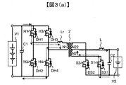
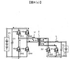
- FIGS. 3 (a) to 3 (d) are circuit diagrams illustrating the operation of the bidirectional DC-DC converter according to the second embodiment during forward power transmission.
- the operation during forward power transmission will be described in detail with reference to FIGS. 3 (a) to 3 (d).
- each of FIGS. 3 (a) to 3 (d) corresponds to modes a to d.
- Mode a As shown in FIG. 3 (a), in mode a, the switching elements H1 and H4 are in the on state, the switching elements H2 and H3 are in the off state, and the voltage of the DC power supply V1 is changed to the switching elements H1 and H4 and the resonant reactor. Applied to the primary winding N1 via Lr.
- the switching element S2 is in an off state, and the voltage generated in the secondary winding N2 is supplied with energy to the DC power supply V2 via the diode DS1 and the smoothing reactor L.
- the loss may be reduced by dividing the current flowing through the diode DS1 to the switching element S1.
- the reduction of the loss by turning on the MOSFET is hereinafter referred to as synchronous rectification.
- This mode d is a symmetrical operation of mode a.
- mode a is a symmetrical operation of mode a.
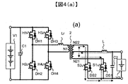
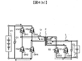
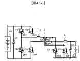
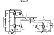
- FIGS. 4 (a) to 4 (e) are circuit diagrams illustrating an operation during reverse power transmission of the bidirectional DC-DC converter according to the second embodiment.
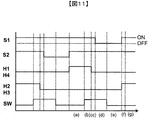
- FIG. 5 is a gate signal waveform diagram of the switching element during reverse power transmission of the bidirectional DC-DC converter according to the second embodiment.
- FIGS. 4 (a) to 4 (e) correspond to the periods (a) to (e) in FIG. 5, and correspond to the following modes a to e.
- Mode a As shown in FIG. 4 (a), in mode a, the switching elements S1 and S2 are turned on, and the voltage of the DC power supply V2 passes through the secondary windings N21 and N22 and the switching elements S1 and S2, and the smoothing reactor. Applied to L, the energy of the DC power source V2 is accumulated in the smoothing reactor L. Since the switching elements H1 to H4 are in the off state and the switching elements S1 and S2 are in the on state, no voltage is applied to the primary winding N1, and the current of the resonant reactor Lr is zero.
- Mode d As shown in FIG. 4D, when the switching element S1 is turned off, the voltage of the DC power source V2 is applied to the secondary winding N22, and the current increases in the resonant reactor Lr. Further, the energy accumulated in the smooth reactor L is released. At this time, because the current flows through the resonant reactor Lr in mode b, the amount of current that increases the current in the resonant reactor Lr in mode d is reduced, and applied to the switching element S1 when the switching element S1 is turned off. Surge voltage is reduced. Note that mode c and mode d may be the same period.
- the DC power source V2 energy is stored in the smoothing reactor L.
- This mode e is a symmetric operation of mode a. Thereafter, since the operation returns to mode a after symmetrical operation of modes b to e, it is assumed that it can be easily understood, and detailed description thereof is omitted.
- Figure 6 shows the voltage and current waveforms during reverse transmission of the bidirectional DC-DC converter according to Example 2.
- the modes b and c are not provided.
- the energy of the smoothing reactor L is applied to the switching element S1 when the switching element S1 is turned off. A maximum of 188.4V) occurred.
- the current flows for the time width in which the switching reactors H1 and H4 are on in the resonant reactor Lr current in the mode d. Therefore, when the switching element S1 is turned off, the power of the smoothing reactor L is not applied to the switching element S1, and the power is supplied to the DC power supply V1, so the surge voltage can be suppressed (maximum 94V). It is.
- the present embodiment it is possible to suppress a surge voltage applied to the switching element during reverse power transmission of the bidirectional DC-DC converter and to provide a bidirectional DC-DC converter with high efficiency, small size, and low cost.
- Example 2 the voltage source full bridge circuit and the current source center tap circuit are combined, but the voltage source push-pull circuit, the current source center tap circuit with active clamp shown in FIG. 12 and other surge absorbing circuits, FIG. Naturally, the combination of the voltage source full bridge circuit and current doubler circuit shown in FIG. 14 and the combination of the voltage source full bridge circuit and current source full bridge circuit shown in FIG.
- FIG. 7 is a circuit configuration diagram of a bidirectional DC-DC converter according to Embodiment 3 of the present invention.
- the same reference numerals as those in the first embodiment have the same functions.
- the same reference numerals as those in the first embodiment have the same functions.
- the first switching leg in which the switching elements H1 and H2 are connected in series is connected to the smoothing capacitor C1 via the diode D0.
- the diode D0 is connected in such a direction as to send power from the first switching leg to the DC power supply V1 and not from the DC power supply V1 to the first switching leg, and a switch SW is connected in parallel to the diode D0.
- the second switching leg in which the switching elements H3 and H4 are connected in series is connected to the smoothing capacitor C1.
- the primary winding N1 and the resonant reactor Lr are connected in series between the series connection point of the switching elements H1 and H2 and the series connection point of the switching elements H3 and H4.
- Forward power transmission keeps the switch SW on. As a result, both ends of the diode D0 are short-circuited, so that the DC terminals of the first switching leg and the second switching leg are in the same state as when directly connected to the smoothing capacitor C1 without passing through the diode D0. .
- This state is the same as the circuit configuration of the second embodiment, and the switching operation is also the same. Therefore, since the operation at the time of forward transmission is the same as that of the second embodiment, the description is omitted.
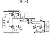
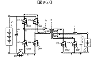
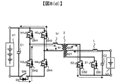
- FIG. 8A to FIG. 8F are circuit diagrams for explaining the operation at the time of reverse power transmission of the bidirectional DC-DC converter in the third embodiment.
- FIG. 9 is a gate signal waveform diagram of the switching element during reverse power transmission of the bidirectional DC-DC converter according to the third embodiment.
- FIGS. 8 (a) to 8 (f) correspond to the periods (a) to (f), respectively, and represent the following modes a to f.
- Mode a As shown in FIG. 8 (a), in mode a, the switching elements S1 and S2 are turned on, and the voltage of the DC power supply V2 passes through the secondary windings N21 and N22 and the switching elements S1 and S2, and the smoothing reactor. Applied to L, the energy of the DC power source V2 is accumulated in the smoothing reactor L.
- the switching elements H1 and H4 are in the on state, the switching elements H2 and H3 are in the off state, and the current passing through the diodes DH2 and DH3, the switching elements H1, H4, and the primary winding N1 flows through the resonance reactor Lr. .
- MOSFETs are used as the switching elements H1 to H4
- synchronous rectification is achieved if the switching elements H2 and H3 are turned on.
- Mode d As shown in FIG. 8 (d), when the switching element S1 is turned off, the voltage of the DC power source V2 is applied to the secondary winding N22, and the current increases in the resonant reactor Lr. Further, the energy accumulated in the smooth reactor L is released. At this time, since the current flows through the resonant reactor Lr in mode b, the amount of current that increases the current in the resonant reactor Lr is reduced in mode d, so the switching element S1 when the switching element S1 is turned off is reduced. The applied surge voltage is reduced. Note that mode c and mode d may be the same period.
- the DC power source V2 energy is stored in the smoothing reactor L.
- the energy of DC power supply V2 is stored in smoothing reactor L.
- This mode f is a symmetrical operation of mode a.
- the operation returns to the mode a after the symmetrical operation of the modes b to f, it will be easily understood, and thus detailed description will be omitted.
- this embodiment allows reverse power transmission from the DC power supply V2 to the DC power supply V1 while suppressing the generation of the surge voltage of the switching elements S1, S2 as in Example 2.
- a synchronous rectification operation can be performed in modes a and f.
- the synchronous rectification operation in which the switching element is turned on can reduce conduction loss as compared with diode rectification, and can achieve higher efficiency of the bidirectional DC-DC converter.
- the present embodiment it is possible to suppress a surge voltage applied to the switching element during reverse power transmission of the bidirectional DC-DC converter and to provide a bidirectional DC-DC converter with high efficiency, small size, and low cost.
- Example 3 the voltage source full bridge circuit and the current source center tap circuit are combined, but the voltage source push-pull circuit, the current source center tap circuit with active clamp shown in FIG. 12 and other surge absorbing circuits, FIG. Naturally, the combination of the voltage source full bridge circuit and current doubler circuit shown in FIG. 14 and the combination of the voltage source full bridge circuit and current source full bridge circuit shown in FIG.
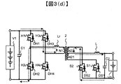
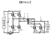
- FIGS. 10 (a) to 10 (g) are a circuit configuration diagram of a bidirectional DC-DC converter according to Embodiment 4 of the present invention and a circuit diagram illustrating an operation during reverse power transmission. Since the circuit configuration of the power conversion device according to the present embodiment is the same as that of Example 3, the description thereof is omitted.
- FIG. 11 is a gate signal waveform diagram of the switching element during reverse power transmission of the bidirectional DC-DC converter according to the fourth embodiment.
- the operation at the time of reverse power transmission will be described in detail with reference to FIGS. 10 (a) to 10 (g) and FIG.
- FIGS. 10 (a) to 10 (g) correspond to the periods (a) to (g) in FIG. 11 and represent the following modes a to g. .
- Mode d As shown in FIG. 10 (d), when the switching element S1 is turned off, the voltage of the DC power source V2 is applied to the secondary winding N22, and the current increases in the resonant reactor Lr. Further, the energy accumulated in the smooth reactor L is released. At this time, since the current flows through the resonant reactor Lr in mode b, the amount of current that increases the current in the resonant reactor Lr is reduced in mode d, so the switching element S1 when the switching element S1 is turned off is reduced. The surge voltage applied to is reduced. Since the switch SW is on, current flows through the switch SW. When using a device such as IGBT that does not allow negative current to flow through the switch SW, current flows through the diode D0. Note that mode c and mode d may be the same period.
- This mode g is a symmetric operation of mode a.
- a detailed description is omitted.
- the present embodiment enables reverse power transmission from the DC power supply V2 to the DC power supply V1 while suppressing the occurrence of surge voltage of the switching elements S1, S2 as in Example 3, and a diode.
- D0 and the switch SW connected in parallel to the diode a synchronous rectification operation can be performed in modes a and f.
- the synchronous rectification operation in which the switching element is turned on can reduce conduction loss as compared with diode rectification, and can achieve higher efficiency of the bidirectional DC-DC converter.
- Embodiment 4 of the present invention can be realized by using an element capable of high-speed switching operation such as a MOSFET as the switching elements H1 to H4. is there. Therefore, the device options for the switch SW increase.
- Example 4 the voltage source full bridge circuit and the current source center tap circuit are combined, but the voltage source push-pull circuit, the current source center tap circuit with active clamp shown in FIG. 12 and other surge absorbing circuits, FIG. Naturally, the combination of the voltage source full bridge circuit and current doubler circuit shown in FIG. 14 and the combination of the voltage source full bridge circuit and current source full bridge circuit shown in FIG.
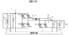
- FIG. 15 is a circuit configuration diagram of the bidirectional DC-DC converter according to the fifth embodiment of the present invention.
- the present embodiment relates to a method of using the bidirectional DC-DC converter in the first to fourth embodiments.
- the high-voltage side of the bidirectional DC-DC converter is the A side
- the low-voltage side is the B side.
- the circuit configuration is such that one end of the HV system device 102 such as a motor drive inverter is connected to one end on the A side of the bidirectional DC-DC converter 101, and the other end of the HV system device 102 is A of the bidirectional DC-DC converter 101. Is connected to the other end.
- One end of the high-voltage battery 104 is connected to one end on the A side of the bidirectional DC-DC converter 101, and the other end of the high-voltage battery 104 is connected to the other end on the A side of the bidirectional DC-DC converter 101 via the relay 106.
- One end of the low voltage battery 105 is connected to one end on the B side of the bidirectional DC-DC converter 101, and the other end of the low voltage battery 105 is connected to the other end on the B side of the bidirectional DC-DC converter 101.
- auxiliary equipment 103 such as an air conditioner is connected to one end on the B side of the bidirectional DC-DC converter, and the other end of the auxiliary equipment 103 is connected to the other end on the B side of the bidirectional DC-DC converter.
- the control means 1 controls the switching operation of the bidirectional DC-DC converter, the power transmission direction, the amount of power, and the like. Note that the relay may not be provided. In the fifth embodiment, there are the following forward power transmission operation and reverse power transmission operation.
- the high voltage battery 104 charges the low voltage battery 105 and supplies power to the auxiliary equipment 103 using a bidirectional DC-DC converter. Note that not only the high-voltage battery 104 but also power from the HV system device 102 may be used.
- the operation of the bidirectional DC-DC converter has a circuit configuration and a control configuration as in the second embodiment, for example.
- the low voltage battery 105 uses a bidirectional DC-DC converter to charge the high voltage battery 104 and supply power to the HV system device 102.
- the bidirectional DC-DC converter has a circuit configuration and a control configuration as in the second embodiment, for example.
- the bidirectional DC-DC converter Since the above-described forward power transmission operation and reverse power transmission operation by the bidirectional DC-DC converter enable bidirectional power conversion, the degree of freedom in designing the vehicle power supply system can be increased. Furthermore, by using the bidirectional DC-DC converter according to the present invention, the surge voltage applied to the switching element in the reverse power transmission operation is suppressed, and a bidirectional DC-DC converter with high efficiency, small size, and low cost can be provided. As a result, it becomes possible to achieve high efficiency, small size and low cost of automobiles.
- the present invention can be applied to all bidirectional DC-DC converters having an insulating function.
- SYMBOLS 1 Control means, 2 ... Transformer, 11 ... 1st switching circuit, 12 ... 2nd switching circuit, 21 ... Voltage sensor, 22 ... Voltage sensor, 31 ... Current sensor, 32 ... Current sensor, 100 ... Car, 101 ... Bidirectional DC-DC converter, 102 ... HV system, 103 ... Auxiliary equipment, 104 ... High voltage battery, 105 ... Low voltage battery, 106 ... Relay, C1 ... Smoothing capacitor, C2 ... Smoothing capacitor, L ... Smoothing reactor, Lr ... Resonant reactor, N1 ... Primary winding, N2 ... Secondary winding, N11 ... Primary winding, N21 ... Secondary winding, N22 ...
Landscapes
- Engineering & Computer Science (AREA)
- Power Engineering (AREA)
- Dc-Dc Converters (AREA)
Abstract
La présente invention traite le problème de la fourniture d'un circuit et de configurations de commande par lesquels une surtension est supprimée pendant une opération d'élévation de tension d'un convertisseur continu-continu bidirectionnel, ce qui permet d'obtenir un convertisseur continu-continu bidirectionnel à haut rendement, compact et à faible coût. Un dispositif de conversion de puissance de la présente invention est un convertisseur continu-continu bidirectionnel permettant d'effectuer une opération d'abaissement de tension ou d'élévation de tension, et comprend : un transformateur dans lequel un enroulement primaire et un enroulement secondaire sont couplés magnétiquement l'un à l'autre ; un premier circuit de commutation qui est connecté électriquement en parallèle à une première alimentation électrique et à l'enroulement primaire ; un second circuit de commutation qui est connecté électriquement en parallèle à une seconde alimentation électrique et à l'enroulement secondaire ; et un circuit de commande permettant de commander le premier circuit de commutation et le second circuit de commutation. Le moyen de commande commande le premier circuit de commutation de façon à élever la tension de l'enroulement primaire en lui fournissant de l'énergie électrique en provenance de la première alimentation électrique avant de transmettre de l'énergie électrique de la seconde alimentation électrique à la première alimentation électrique par l'intermédiaire du transformateur.
Applications Claiming Priority (2)
| Application Number | Priority Date | Filing Date | Title |
|---|---|---|---|
| JP2016-094987 | 2016-05-11 | ||
| JP2016094987A JP6742145B2 (ja) | 2016-05-11 | 2016-05-11 | 双方向dc−dcコンバータ、これを用いた電源システム及び当該電源システムを用いた自動車 |
Publications (1)
| Publication Number | Publication Date |
|---|---|
| WO2017195511A1 true WO2017195511A1 (fr) | 2017-11-16 |
Family
ID=60267013
Family Applications (1)
| Application Number | Title | Priority Date | Filing Date |
|---|---|---|---|
| PCT/JP2017/014481 Ceased WO2017195511A1 (fr) | 2016-05-11 | 2017-04-07 | Convertisseur continu-continu bidirectionnel, système d'alimentation électrique l'utilisant et automobile utilisant le système d'alimentation électrique |
Country Status (2)
| Country | Link |
|---|---|
| JP (1) | JP6742145B2 (fr) |
| WO (1) | WO2017195511A1 (fr) |
Cited By (2)
| Publication number | Priority date | Publication date | Assignee | Title |
|---|---|---|---|---|
| CN114175481A (zh) * | 2019-07-18 | 2022-03-11 | Ls电气株式会社 | 电力转换系统的dc-dc转换器 |
| US20230133167A1 (en) * | 2021-10-29 | 2023-05-04 | Mitsubishi Heavy Industries, Ltd. | Bidirectional dc-dc converter, traffic system, control method, and non-transitory computer-readable storage medium |
Families Citing this family (6)
| Publication number | Priority date | Publication date | Assignee | Title |
|---|---|---|---|---|
| CN109861539B (zh) * | 2017-11-30 | 2022-02-08 | 比亚迪股份有限公司 | 电动汽车及其电源电路 |
| US10833511B2 (en) * | 2017-12-07 | 2020-11-10 | National Chung Shan Institute Of Science And Technology | Battery cell management and balance circuit, method, and battery system |
| US10807487B2 (en) * | 2017-12-11 | 2020-10-20 | National Chung Shan Institute Of Science And Technology | Battery management and balance circuit, battery system and method of charging the battery system |
| CN112421961A (zh) * | 2020-10-30 | 2021-02-26 | 杭州富特科技股份有限公司 | 具有反向预充电功能的车载dc/dc变换器及车载充电装置 |
| JP7752040B2 (ja) * | 2021-03-30 | 2025-10-09 | Tdk株式会社 | 電力変換装置および電力変換システム |
| US12341435B2 (en) | 2021-03-30 | 2025-06-24 | Tdk Corporation | Power conversion apparatus and power conversion system |
Citations (3)
| Publication number | Priority date | Publication date | Assignee | Title |
|---|---|---|---|---|
| JP2012110108A (ja) * | 2010-11-16 | 2012-06-07 | Tdk Corp | スイッチング電源装置 |
| JP2013031368A (ja) * | 2012-11-09 | 2013-02-07 | Hitachi Computer Peripherals Co Ltd | 双方向dc−dcコンバータ |
| JP2016226252A (ja) * | 2015-06-01 | 2016-12-28 | 住友電気工業株式会社 | 電力変換装置及び電力変換装置の制御方法 |
-
2016
- 2016-05-11 JP JP2016094987A patent/JP6742145B2/ja active Active
-
2017
- 2017-04-07 WO PCT/JP2017/014481 patent/WO2017195511A1/fr not_active Ceased
Patent Citations (3)
| Publication number | Priority date | Publication date | Assignee | Title |
|---|---|---|---|---|
| JP2012110108A (ja) * | 2010-11-16 | 2012-06-07 | Tdk Corp | スイッチング電源装置 |
| JP2013031368A (ja) * | 2012-11-09 | 2013-02-07 | Hitachi Computer Peripherals Co Ltd | 双方向dc−dcコンバータ |
| JP2016226252A (ja) * | 2015-06-01 | 2016-12-28 | 住友電気工業株式会社 | 電力変換装置及び電力変換装置の制御方法 |
Cited By (5)
| Publication number | Priority date | Publication date | Assignee | Title |
|---|---|---|---|---|
| CN114175481A (zh) * | 2019-07-18 | 2022-03-11 | Ls电气株式会社 | 电力转换系统的dc-dc转换器 |
| CN114175481B (zh) * | 2019-07-18 | 2024-03-22 | Ls电气株式会社 | 电力转换系统的dc-dc转换器 |
| US12040713B2 (en) | 2019-07-18 | 2024-07-16 | Ls Electric Co., Ltd. | DC-DC converter of power conversion system |
| US20230133167A1 (en) * | 2021-10-29 | 2023-05-04 | Mitsubishi Heavy Industries, Ltd. | Bidirectional dc-dc converter, traffic system, control method, and non-transitory computer-readable storage medium |
| US12328076B2 (en) * | 2021-10-29 | 2025-06-10 | Mitsubishi Heavy Industries, Ltd. | Bidirectional DC-DC converter, traffic system, control method, and non-transitory computer-readable storage medium |
Also Published As
| Publication number | Publication date |
|---|---|
| JP2017204925A (ja) | 2017-11-16 |
| JP6742145B2 (ja) | 2020-08-19 |
Similar Documents
| Publication | Publication Date | Title |
|---|---|---|
| JP6742145B2 (ja) | 双方向dc−dcコンバータ、これを用いた電源システム及び当該電源システムを用いた自動車 | |
| KR101200554B1 (ko) | 다상 인터리브 양방향 dc―dc 컨버터 | |
| JP6057186B2 (ja) | バッテリ充電装置 | |
| JP4401418B2 (ja) | 双方向dc/dcコンバータおよびパワーコンディショナ | |
| JP5630409B2 (ja) | プッシュプル回路、dc/dcコンバータ、ソーラー充電システム、及び移動体 | |
| JP5855133B2 (ja) | 充電装置 | |
| US9209698B2 (en) | Electric power conversion device | |
| JP2015159711A (ja) | スイッチング電源装置、電力変換装置 | |
| WO2016194790A1 (fr) | Dispositif convertisseur de puissance électrique et procédé de commande de dispositif convertisseur de puissance électrique | |
| WO2012168983A1 (fr) | Dispositif de charge | |
| EP2695763A2 (fr) | Convertisseur de puissance de traction pour véhicule ferroviaire multisystème | |
| US20150043251A1 (en) | Power conversion system and method of controlling power conversion system | |
| JPWO2013076752A1 (ja) | Dc/dcコンバータ | |
| JP5412515B2 (ja) | 電源装置 | |
| JP2016123193A (ja) | 電源システム、車両及び電圧制御方法 | |
| JP5881553B2 (ja) | 双方向dc/dcコンバータおよびこれを用いた車両用電源装置 | |
| JP6953634B2 (ja) | Dc/dcコンバータを備える車両充電器 | |
| US11936297B2 (en) | DC-DC converter including first and second coils magnetically coupled such that current flows through second coil in forward direction of diode by mutual induction as current flowing through first coil from intermediate terminal to output terminal increases and vehicle | |
| JP2012157118A (ja) | 電力変換装置 | |
| JP6668056B2 (ja) | 電力変換装置、これを用いた電源システム及び自動車 | |
| WO2017051814A1 (fr) | Dispositif d'alimentation électrique | |
| JP2015139312A (ja) | スイッチング電源装置、電力変換装置 | |
| WO2018070185A1 (fr) | Convertisseur continu-continu et automobile | |
| JP2025138279A (ja) | 電圧変換装置 | |
| WO2024166428A1 (fr) | Dispositif de conversion de puissance |
Legal Events
| Date | Code | Title | Description |
|---|---|---|---|
| NENP | Non-entry into the national phase |
Ref country code: DE |
|
| 121 | Ep: the epo has been informed by wipo that ep was designated in this application |
Ref document number: 17795872 Country of ref document: EP Kind code of ref document: A1 |
|
| 122 | Ep: pct application non-entry in european phase |
Ref document number: 17795872 Country of ref document: EP Kind code of ref document: A1 |