WO2017195560A1 - Dispositif d'affichage et dispositif électronique - Google Patents
Dispositif d'affichage et dispositif électronique Download PDFInfo
- Publication number
- WO2017195560A1 WO2017195560A1 PCT/JP2017/015896 JP2017015896W WO2017195560A1 WO 2017195560 A1 WO2017195560 A1 WO 2017195560A1 JP 2017015896 W JP2017015896 W JP 2017015896W WO 2017195560 A1 WO2017195560 A1 WO 2017195560A1
- Authority
- WO
- WIPO (PCT)
- Prior art keywords
- electrode
- sub
- electrodes
- display device
- pixel
- Prior art date
- Legal status (The legal status is an assumption and is not a legal conclusion. Google has not performed a legal analysis and makes no representation as to the accuracy of the status listed.)
- Ceased
Links
Images






Classifications
-
- H—ELECTRICITY
- H10—SEMICONDUCTOR DEVICES; ELECTRIC SOLID-STATE DEVICES NOT OTHERWISE PROVIDED FOR
- H10K—ORGANIC ELECTRIC SOLID-STATE DEVICES
- H10K59/00—Integrated devices, or assemblies of multiple devices, comprising at least one organic light-emitting element covered by group H10K50/00
- H10K59/10—OLED displays
- H10K59/12—Active-matrix OLED [AMOLED] displays
- H10K59/122—Pixel-defining structures or layers, e.g. banks
-
- H—ELECTRICITY
- H10—SEMICONDUCTOR DEVICES; ELECTRIC SOLID-STATE DEVICES NOT OTHERWISE PROVIDED FOR
- H10K—ORGANIC ELECTRIC SOLID-STATE DEVICES
- H10K50/00—Organic light-emitting devices
- H10K50/80—Constructional details
- H10K50/805—Electrodes
- H10K50/81—Anodes
- H10K50/813—Anodes characterised by their shape
-
- H—ELECTRICITY
- H10—SEMICONDUCTOR DEVICES; ELECTRIC SOLID-STATE DEVICES NOT OTHERWISE PROVIDED FOR
- H10K—ORGANIC ELECTRIC SOLID-STATE DEVICES
- H10K50/00—Organic light-emitting devices
- H10K50/80—Constructional details
- H10K50/805—Electrodes
- H10K50/82—Cathodes
- H10K50/822—Cathodes characterised by their shape
-
- H—ELECTRICITY
- H10—SEMICONDUCTOR DEVICES; ELECTRIC SOLID-STATE DEVICES NOT OTHERWISE PROVIDED FOR
- H10K—ORGANIC ELECTRIC SOLID-STATE DEVICES
- H10K50/00—Organic light-emitting devices
- H10K50/80—Constructional details
- H10K50/84—Passivation; Containers; Encapsulations
- H10K50/844—Encapsulations
-
- H—ELECTRICITY
- H10—SEMICONDUCTOR DEVICES; ELECTRIC SOLID-STATE DEVICES NOT OTHERWISE PROVIDED FOR
- H10K—ORGANIC ELECTRIC SOLID-STATE DEVICES
- H10K59/00—Integrated devices, or assemblies of multiple devices, comprising at least one organic light-emitting element covered by group H10K50/00
- H10K59/80—Constructional details
- H10K59/805—Electrodes
- H10K59/8051—Anodes
- H10K59/80515—Anodes characterised by their shape
-
- H—ELECTRICITY
- H10—SEMICONDUCTOR DEVICES; ELECTRIC SOLID-STATE DEVICES NOT OTHERWISE PROVIDED FOR
- H10K—ORGANIC ELECTRIC SOLID-STATE DEVICES
- H10K59/00—Integrated devices, or assemblies of multiple devices, comprising at least one organic light-emitting element covered by group H10K50/00
- H10K59/80—Constructional details
- H10K59/805—Electrodes
- H10K59/8051—Anodes
- H10K59/80518—Reflective anodes, e.g. ITO combined with thick metallic layers
-
- H—ELECTRICITY
- H10—SEMICONDUCTOR DEVICES; ELECTRIC SOLID-STATE DEVICES NOT OTHERWISE PROVIDED FOR
- H10K—ORGANIC ELECTRIC SOLID-STATE DEVICES
- H10K71/00—Manufacture or treatment specially adapted for the organic devices covered by this subclass
-
- H—ELECTRICITY
- H10—SEMICONDUCTOR DEVICES; ELECTRIC SOLID-STATE DEVICES NOT OTHERWISE PROVIDED FOR
- H10K—ORGANIC ELECTRIC SOLID-STATE DEVICES
- H10K2102/00—Constructional details relating to the organic devices covered by this subclass
- H10K2102/301—Details of OLEDs
- H10K2102/341—Short-circuit prevention
-
- H—ELECTRICITY
- H10—SEMICONDUCTOR DEVICES; ELECTRIC SOLID-STATE DEVICES NOT OTHERWISE PROVIDED FOR
- H10K—ORGANIC ELECTRIC SOLID-STATE DEVICES
- H10K50/00—Organic light-emitting devices
- H10K50/80—Constructional details
- H10K50/805—Electrodes
- H10K50/81—Anodes
- H10K50/818—Reflective anodes, e.g. ITO combined with thick metallic layers
-
- H—ELECTRICITY
- H10—SEMICONDUCTOR DEVICES; ELECTRIC SOLID-STATE DEVICES NOT OTHERWISE PROVIDED FOR
- H10K—ORGANIC ELECTRIC SOLID-STATE DEVICES
- H10K50/00—Organic light-emitting devices
- H10K50/80—Constructional details
- H10K50/85—Arrangements for extracting light from the devices
- H10K50/856—Arrangements for extracting light from the devices comprising reflective means
-
- H—ELECTRICITY
- H10—SEMICONDUCTOR DEVICES; ELECTRIC SOLID-STATE DEVICES NOT OTHERWISE PROVIDED FOR
- H10K—ORGANIC ELECTRIC SOLID-STATE DEVICES
- H10K59/00—Integrated devices, or assemblies of multiple devices, comprising at least one organic light-emitting element covered by group H10K50/00
- H10K59/80—Constructional details
- H10K59/87—Passivation; Containers; Encapsulations
- H10K59/873—Encapsulations
-
- H—ELECTRICITY
- H10—SEMICONDUCTOR DEVICES; ELECTRIC SOLID-STATE DEVICES NOT OTHERWISE PROVIDED FOR
- H10K—ORGANIC ELECTRIC SOLID-STATE DEVICES
- H10K59/00—Integrated devices, or assemblies of multiple devices, comprising at least one organic light-emitting element covered by group H10K50/00
- H10K59/80—Constructional details
- H10K59/875—Arrangements for extracting light from the devices
- H10K59/878—Arrangements for extracting light from the devices comprising reflective means
-
- H—ELECTRICITY
- H10—SEMICONDUCTOR DEVICES; ELECTRIC SOLID-STATE DEVICES NOT OTHERWISE PROVIDED FOR
- H10K—ORGANIC ELECTRIC SOLID-STATE DEVICES
- H10K71/00—Manufacture or treatment specially adapted for the organic devices covered by this subclass
- H10K71/861—Repairing
Definitions
- the present disclosure relates to a display device using an organic EL (electroluminescence) element and an electronic apparatus including the display device.
- an anode and a cathode may be electrically short-circuited to cause a pixel defect called a dark spot.
- a technique for repairing (repairing) such a short-circuited portion has been proposed (for example, Patent Document 1).
- a display device includes a plurality of pixels, and each of the plurality of pixels is formed on the first electrode including the plurality of sub-electrodes and the plurality of sub-electrodes.
- An insulating film having an opening facing each other, an organic layer formed in each opening of the insulating film and including a light emitting layer, and a second electrode formed on the organic layer.
- An electronic apparatus includes the display device according to the embodiment of the present disclosure.
- the first electrode includes a plurality of sub-electrodes, so that in the selective pixel, the first electrode and the second electrode are electrically connected to each other due to foreign matters. Even when short-circuited, a part of the sub-electrode corresponding to the short-circuited portion can be selectively cut.
- an image is displayed by the display device according to the embodiment of the present disclosure.
- the first electrode in each pixel, includes a plurality of sub-electrodes, and the insulating film has an opening facing each sub-electrode.
- An organic layer is formed in the opening.
- FIG. 1 is a block diagram illustrating an overall configuration of a display device according to an embodiment of the present disclosure.
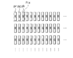
- FIG. 2 is a schematic diagram illustrating an arrangement of pixels illustrated in FIG. 1.
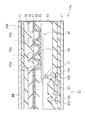
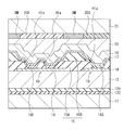
- FIG. 2 is a cross-sectional view illustrating a partial configuration of a pixel portion illustrated in FIG. 1.
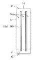
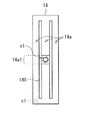
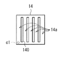
- FIG. 4 is a plan view illustrating a configuration example of a first electrode illustrated in FIG. 3.
- FIG. 4 is a plan view illustrating a configuration of a first insulating film illustrated in FIG. 3 together with a configuration of a first electrode.
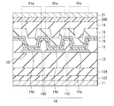
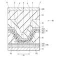
- FIG. 6 is a cross-sectional view illustrating a configuration corresponding to the line IB-IB in FIG. 5. It is sectional drawing showing the detailed structure of the opening part (reflector) shown in FIG.
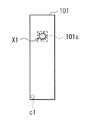
- FIG. 10 is a schematic diagram for explaining defect repair according to Comparative Example 1.
- FIG. 10 is a schematic diagram for explaining defect repair according to Comparative Example 2.
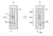
- FIG. It is a schematic diagram for demonstrating the effect by the defect repair shown in FIG.
- FIG. It is a schematic diagram for demonstrating the effect by the opening part shown in FIG. 3 and
- FIG. 10 is a plan view illustrating a configuration of a first electrode according to Modification 1-1.
- FIG. 12 is a plan view illustrating a configuration of a first electrode according to Modification 1-2.
- FIG. 10 is a plan view illustrating a configuration of a first electrode according to Modification 1-3.
- FIG. 14 is a plan view illustrating a configuration of a first electrode according to Modification 2-1.
- FIG. 14 is a plan view illustrating a configuration of a first electrode according to Modification 2-2.
- FIG. 12 is a plan view illustrating a configuration of a first electrode according to Modification 3-1.
- FIG. 12 is a plan view illustrating a configuration of a first electrode according to Modification 3-2.
- FIG. 10 is a plan view illustrating a configuration of a first electrode according to Modification 4.
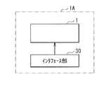
- FIG. 10 is a cross-sectional view illustrating a configuration of a pixel unit according to Modification Example 5. It is a block diagram showing the function structure of the example of application.
- Embodiment Example of display device in which first electrode is divided into a plurality of sub-electrodes and an opening having a reflector is provided for each sub-electrode
- Modifications 1-1 to 1-3 (Other examples of sub electrode stripe arrangement) 3.
- Modified examples 2-1 and 2-2 (examples where the surface shape of the sub-electrode is circular or elliptical) 4).
- Modified examples 3-1 and 3-2 other examples of sub-electrode dividing directions) 5.
- Modification 4 (Another example of the surface shape of the first electrode) 6).
- Modification 5 (Other configuration example of the pixel portion) 7).
- Application examples (examples of electronic devices)
- FIG. 1 illustrates an overall configuration of a display device (display device 1) according to an embodiment of the present disclosure.
- the display device 1 is, for example, an organic EL display using an organic electroluminescence element, and for example, light of any color of R (red), G (green), and B (blue) is emitted from the upper surface side.
- the display device 1 includes, for example, a pixel unit 2 and a circuit unit (scanning line driving unit 3, signal line driving unit 4, and power supply line driving unit 5) for driving the pixel unit 2.
- the pixel unit 2 has a plurality of pixels pr, pg, and pb that are two-dimensionally arranged.
- the pixel unit 2 displays an image based on a video signal input from the outside by, for example, an active matrix method.
- the pixel unit 2 includes a plurality of scanning lines WSL extending along the row direction of the pixel array, a plurality of signal lines DTL extending along the column direction, and a plurality of signal lines DTL extending along the row direction.
- a power supply line DSL is provided.
- These scanning lines WSL, signal lines DTL, and power supply lines DSL are electrically connected to the pixels pr, pg, pb.
- Each of the pixels pr, pg, and pb corresponds to, for example, a subpixel, and a set of these pixels pr, pg, and pb constitutes one pixel (pixel Pix).
- FIG. 2 shows an example of a planar configuration of the pixel Pix (pixels pr, pg, pb) shown in FIG.
- Each surface shape of the pixels pr, pg, pb has a rectangular shape, for example, and is arranged in a stripe shape as a whole.
- pixels having the same emission color are arranged side by side.
- the pixel pr is for displaying red (R)
- the pixel pg is for displaying green (G), for example
- the pixel pb is for displaying blue (B), for example.
- Each of these pixels pr, pg, and pb has a pixel circuit PXLC including the organic EL element 10.
- pixels P when it is not necessary to distinguish each of the pixels pr, pg, and pb, they will be referred to as “pixels P”.
- the pixel circuit PXLC controls light emission and extinction in each pixel pr, pg, pb, and includes, for example, an organic EL element 10, a storage capacitor Cs, a write transistor WsTr, and a drive transistor DsTr. Yes.
- the circuit configuration of 2Tr1C is illustrated as the pixel circuit PXLC, but the configuration of the pixel circuit PXLC is not limited to this.
- the pixel circuit PXLC may have a circuit configuration in which various capacitors, transistors, and the like are further added to the 2Tr1C circuit.
- the write transistor WsTr controls application of a video signal (signal voltage) to the gate electrode of the drive transistor DsTr. Specifically, the write transistor WsTr samples the voltage (signal voltage) of the signal line DTL according to the voltage applied to the scanning line WSL, and writes the signal voltage to the gate electrode of the drive transistor DsTr.
- the drive transistor DsTr is connected in series to the organic EL element 10 and controls the current flowing through the organic EL element 10 according to the magnitude of the signal voltage sampled by the write transistor WsTr.
- the drive transistor DsTr and the write transistor WsTr are formed by, for example, an n-channel MOS type or a p-channel MOS type thin film transistor (TFT: Thin Film Transistor). These drive transistor DsTr and write transistor WsTr may be a single gate type or a dual gate type.
- the holding capacitor Cs holds a predetermined voltage between the gate electrode and the source electrode of the driving transistor DsTr.
- the gate electrode of the writing transistor WsTr is connected to the scanning line WSL.
- One of the source electrode and the drain electrode of the write transistor WsTr is connected to the signal line DTL, and the other electrode is connected to the gate electrode of the drive transistor DsTr.
- One of the source electrode and the drain electrode of the drive transistor DsTr is connected to the power supply line DSL, and the other electrode is connected to an anode (first electrode 14 described later) of the organic EL element 10.
- the storage capacitor Cs is inserted between the gate electrode of the drive transistor DsTr and the electrode on the organic EL element 10 side.
- the scanning line WSL is for supplying each pixel P with a selection pulse for selecting a plurality of pixels P arranged in the pixel unit 2 for each row.
- the scanning line WSL is connected to an output end (not shown) of the scanning line driving unit 3 and a gate electrode of a writing transistor WsTr described later.
- the signal line DTL is for supplying a signal pulse (signal potential Vsig and reference potential Vofs) corresponding to the video signal to each pixel P.
- the signal line DTL is connected to an output end (not shown) of the signal line driver 4 and a source electrode or a drain electrode of a write transistor WsTr described later.
- the power supply line DSL is for supplying a fixed potential (Vcc) to each pixel P as electric power.
- the power supply line DSL is connected to an output end (not shown) of the power supply line driving unit 5 and a source electrode or a drain electrode of a drive transistor DsTr described later.
- the cathode (second electrode 17 described later) of the organic EL element 10 is connected to a common potential line (cathode line).
- the scanning line driving unit 3 outputs a predetermined selection pulse to each scanning line WSL in a line-sequential manner, thereby performing operations such as anode reset, Vth correction, signal potential Vsig writing, mobility correction, and light emission operation, for example.
- Each pixel P is executed at a predetermined timing.
- the signal line drive unit 4 generates an analog video signal corresponding to a digital video signal input from the outside, and outputs the analog video signal to each signal line DTL.
- the power line driver 5 outputs a constant potential to each power line DSL.
- the scanning line driving unit 3, the signal line driving unit 4, and the power supply line driving unit 5 are controlled so as to operate in conjunction with each other by a timing control signal output from a timing control unit (not shown).
- a digital video signal input from the outside is corrected by a video signal receiving unit (not shown) and then input to the signal line driving unit 4.
- FIG. 3 shows a partial cross-sectional configuration of the display device 1 (pixel unit 2).
- a plurality of organic EL elements 10 are two-dimensionally arranged on the drive substrate 11a.
- a region corresponding to one organic EL element 10 (corresponding to a pixel pr that displays red). (Region) only.
- the second substrate 21 is interposed via a second insulating film 18, a sealing layer 19, a color filter layer (red filter 20R, green filter 20G, blue filter 20B) and a black matrix layer BM. Are pasted together.
- the drive substrate 11a is obtained by forming a pixel circuit including the TFT 12 (the pixel circuit PXLC shown in FIG. 1) on the first substrate 11 made of, for example, glass or plastic.
- the surface of the drive substrate 11a is flattened by the flattening film 13.
- the TFT 12 corresponds to, for example, the drive transistor DsTr shown in FIG.
- the TFT 12 has, for example, a gate electrode 121 in a selective region on the first substrate 11, and a semiconductor layer 123 on the gate electrode 121 through a gate insulating film 122.
- An interlayer insulating film 124 is formed on the semiconductor layer 123.
- a pair of source / drain electrodes 125 is provided on the interlayer insulating film 124. These source / drain electrodes 125 are electrically connected to the semiconductor layer 123 through contact holes provided in the interlayer insulating film 124.
- One of the pair of source / drain electrodes 125 is electrically connected to the first electrode 14 through a contact portion c1 (anode contact).
- the TFT 12 has a so-called bottom gate structure as an example.
- the present invention is not limited to this, and the TFT 12 may have a so-called top gate structure.
- the gate electrode 121 includes at least one of metals such as molybdenum (Mo), titanium (Ti), aluminum (Al), tungsten (W), and chromium (Cr).
- the gate insulating film 122 and the interlayer insulating film 124 include, for example, at least one of silicon oxide (SiO 2 ), silicon nitride (SiNx), silicon oxynitride (SiON), and the like.
- the semiconductor layer 123 is formed of a silicon-based semiconductor such as amorphous silicon (amorphous silicon), polycrystalline silicon (polysilicon), and microcrystalline silicon, or an oxide such as indium gallium zinc oxide (InGaZnO) and zinc oxide (ZnO). It is composed of a physical semiconductor.
- the source / drain electrode 125 is configured to include at least one of metals such as molybdenum, titanium, aluminum, tungsten, and chromium.
- the planarizing film 13 is made of, for example, an organic insulating material such as polyimide or acrylic resin.
- the organic EL element 10 On the driving substrate 11a, the organic EL element 10 is formed for each of the pixels pr, pg, and pb. As shown in FIG. 3, the organic EL element 10 has an organic layer 16 and a second electrode 17 on the first electrode 14. A plurality of first electrodes 14 are arranged on the drive substrate 11a, and a first insulating film 15 (insulating film) is formed so as to cover the plurality of first electrodes 14. The first insulating film 15 has a plurality of openings (openings H1a) facing each first electrode 14. The organic layer 16 is formed in each opening H1a of the first insulating film 15.
- the first electrode 14 is, for example, a reflective electrode that functions as an anode, and is provided for each pixel P.
- the constituent material of the first electrode 14 include metal elements such as aluminum (Al), chromium, gold (Au), platinum (Pt), nickel (Ni), copper (Cu), tungsten, or silver (Ag).
- metal elements such as aluminum (Al), chromium, gold (Au), platinum (Pt), nickel (Ni), copper (Cu), tungsten, or silver (Ag).
- a simple substance or an alloy is mentioned.
- the first electrode 14 may include a laminated film of a metal film made of a single element or an alloy of these metal elements and a light-transmitting conductive material (transparent conductive film).
- the transparent conductive film include ITO (indium tin oxide), IZO (indium zinc oxide), and zinc oxide (ZnO) based materials.
- zinc oxide-based material include zinc oxide (AZO) to which aluminum (Al) is added and zinc oxide
- FIG. 4 shows a planar configuration of the first electrode 14.
- the first electrode 14 is divided (subdivided) and includes a plurality of sub-electrodes (sub-electrode portions) 14a.
- three sub-electrodes 14a are arranged in a region A of the first electrode 14 that contributes to light emission.
- Each sub-electrode 14a is disposed to face the opening H1a of the first insulating film 15.
- These three sub-electrodes 14a are connected (electrically connected) at the end portions (end portions e1 and e2) of the first electrode 14.
- the first electrode 14 has a plurality of (here, two) slits 140, and each slit 140 extends along the long side direction of the rectangular shape of the first electrode 14.
- the first electrode 14 (specifically, a part of the first electrode 14) is divided into a plurality of sub-electrodes 14a.
- the dividing direction in the region A is along the rectangular long side direction of the first electrode 14.
- a part of the first electrode 14 (a region 14a1 corresponding to a short-circuited portion on a sub electrode 14a described later) is selectively cut.
- the surface shape of the first electrode 14 (the shape of the surface parallel to the substrate surface) is, for example, a rectangular shape.
- the surface shape of the sub-electrode 14a is not particularly limited.
- the sub-electrode 14a has a rectangular shape having long sides along the long-side direction of the rectangular shape of the first electrode 14.
- a plurality of sub-electrodes 14a are arranged in a stripe shape, for example.
- each sub-electrode 14a has a rectangular shape extending along one direction (arranged extending straight along one direction), but each sub-electrode 14a is meanderingly arranged. Alternatively, they may be arranged in a zigzag shape. Further, it may be bent or curved in part.
- the width, size, shape, and the like of the sub-electrodes 14a may be the same or different.
- the first insulating film 15 is for defining the light emitting region of each pixel P and ensuring the insulation between the first electrode 14 and the second electrode 17.
- the first insulating film 15 also functions as a so-called partition wall when the organic layer 16 is formed using a wet process.
- the first insulating film 15 is, for example, a photosensitive resin such as an acrylic resin, a polyimide resin, a fluorine resin, a silicon resin, a fluorine polymer, a silicon polymer, a novolac resin, an epoxy resin, or a norbornene resin. It is comprised including. Or what disperse
- the first insulating film 15 may be made of an inorganic material such as silicon oxide, silicon nitride, or silicon oxynitride.
- FIG. 5 shows the planar configuration of the first insulating film 15 together with the planar configuration of the first electrode 14.
- FIG. 6 shows a cross-sectional configuration taken along line IB-IB in FIG.
- the configuration shown in FIG. 3 corresponds to the cross-sectional configuration taken along the line IA-IA in FIG.
- the first insulating film 15 has a plurality (three in this case) of openings H1a facing one first electrode 14.
- Each opening H1a is disposed to face the sub electrode 14a (a region of the first insulating film 15 facing the sub electrode 14a is opened).
- On the bottom surface of each opening H1a for example, the sub electrode 14a, the organic layer 16, and the second electrode 17 are stacked in this order.
- one organic EL element 10 has three effective light emitting regions defined by the three openings H1a.
- the opening H1a of the first insulating film 15 desirably has a reflector (reflection structure) 40 as described below, for example. This is because the light extraction efficiency can be improved and the luminance can be increased (decrease in luminance due to dark spots can be suppressed).
- FIG. 7 shows a detailed configuration in the vicinity of the opening H1a.
- the reflector 40 has a function of guiding the light generated from the organic layer 16 toward the front by reflection using a reflection interface formed in the vicinity of the inclined surface PS of the first insulating film 15.
- the reflector 40 includes, for example, the constituent material (refractive index) of the first insulating film 15, the shape and the inclination angle ⁇ of the inclined surface PS of the opening H1a, and the constituent materials (second insulating film 18 and the sealing layer 19). (Refractive index) and the combination.
- the first electrode 14 (sub-electrode 14 a) has a laminated structure of an Al alloy layer 141 and an ITO layer 142. As the organic layer 16, hole injection is sequentially performed from the first electrode 14 side. The case where the transport layer 161, the light emitting layer 162, and the electron transport layer 163 are formed is shown.
- the refractive index of the first insulating film 15 is preferably different from the refractive index of the second insulating film 18. This is because a reflective interface is formed by the difference in refractive index between the first insulating film 15 and the second insulating film 18. It is desirable that the refractive index n2 of the second insulating film 18 and the refractive index n1 of the first insulating film 15 satisfy the following expressions (1) and (2). Thereby, light can be efficiently reflected at the reflection interface between the first insulating film 15 and the second insulating film 18.
- the thickness (height) t of the first insulating film 15, the opening length R1 on the lower end side of the opening H1a, and the opening length R2 on the upper end side of the opening H1a are expressed by the following equations (3) and ( It is desirable to satisfy 4). Thereby, light can be efficiently reflected at the reflection interface between the first insulating film 15 and the second insulating film 18.
- the organic layer 16 includes, for example, an organic electroluminescent layer (light emitting layer) that generates white light, and is formed as a common layer for a plurality of pixels pr, pg, pb in the pixel unit 2, for example.
- the organic layer 16 may include, for example, a hole injection layer, a hole transport layer, and an electron transport layer as necessary.
- the light emitting layer included in the organic layer 16 has a configuration in which, for example, a red light emitting layer, a green light emitting layer, and a blue light emitting layer are stacked. Or you may have the structure which laminated
- the light emitting layer may be formed as a light emitting layer having a different color for each of the pixels pr, pg, and pb.
- the organic layer 16 formed in the pixel pr includes a red light emitting layer
- the organic layer 16 formed in the pixel pg includes a green light emitting layer
- the organic layer 16 formed in the pixel pb includes a blue light emitting layer. Formed with.
- the second electrode 17 functions as, for example, a cathode, and is formed over the entire surface of the pixel portion 2 (as an electrode common to all the pixels P).
- the second electrode 17 is made of, for example, a transparent conductive film.
- the transparent conductive film include ITO (indium tin oxide), IZO (indium zinc oxide), and zinc oxide (ZnO) based materials.
- the zinc oxide-based material include zinc oxide (AZO) to which aluminum (Al) is added and zinc oxide (GZO) to which gallium (Ga) is added.
- the thickness of the second electrode 17 is not particularly limited, but may be set in consideration of conductivity and light transmittance. In addition to this, an alloy of magnesium and silver (MgAg alloy) may be used for the second electrode 17.
- the second insulating film 18 is provided so as to cover the second electrode 17 and is made of, for example, silicon nitride.
- the second insulating film 18 is provided to increase the reflection efficiency of the reflector 40, and as a protective film for preventing moisture from entering the organic EL element 10 and preventing changes in characteristics such as light emission efficiency. It also has the function of
- the sealing layer 19 seals the organic EL element 10 while bonding the second insulating film 18 and the second substrate 21 together.
- the material of the sealing layer 19 include acrylic resins, polyimide resins, fluorine resins, silicon resins, fluorine polymers, silicon polymers, novolac resins, epoxy resins, and norbornene resins. . Or what disperse
- the color filter layers extract white light generated in each organic EL element 10 as red (R), green (G), and blue (B) color lights. And provided on one surface of the second substrate 21 (for example, the surface on the sealing layer 19 side).
- a red filter 20R is formed in a region facing the organic EL element 10 of the pixel pr
- a green filter 20G is formed in a region facing the organic EL element 10 of the pixel pg
- a blue filter 20B is formed in a region facing the organic EL element 10 of the pixel pb.
- These red filter 20R, green filter 20G, and blue filter 20B are each composed of a resin mixed with a pigment.
- the black matrix layer BM is formed in a region (region between pixels) between the red filter 20R, the green filter 20G, and the blue filter 20B.
- the black matrix layer BM is constituted by, for example, a resin film mixed with a black colorant, or a thin film filter using thin film interference.
- the thin film filter is formed by, for example, laminating one or more thin films made of metal, metal nitride, or metal oxide, and attenuating light by utilizing interference of the thin film.
- Specific examples of the thin film filter include a filter in which Cr and chromium oxide (III) (Cr 2 O 3 ) are alternately laminated.
- the second substrate 21 seals the organic EL element 10 together with the sealing layer 19.
- the second substrate 21 is made of, for example, a material such as glass or plastic that is transparent to the light generated in the organic EL element 10.
- the first electrode 14 includes a plurality of sub-electrodes 14a.
- a description will be given of defect repair when an electrical short circuit (short circuit x1) occurs due to a foreign object.
- a part of the first electrode 14 including a part where the short circuit x1 occurs (a part where foreign matter is mixed) (partial region 14a1 of the sub-electrode 14a). Is selectively disconnected.
- the laser used for the repair is not particularly limited, and examples thereof include a laser capable of processing the metal constituting the first electrode 14 or the transparent conductive film, for example, a solid-state laser such as a fiber laser or a YAG laser.
- Comparative Examples 1 and 2 of the present embodiment defect repair when the first electrode (first electrode 101) is not divided will be described.
- the location (part 101a) where the short circuit x1 occurs is selectively cut by laser irradiation.
- the laser beam is scanned along the portion 101a including the short circuit x1 (so as to surround the portion where the short circuit x1 occurs), and the repair is not easy.
- an insulating film 102 having, for example, two openings 102a is provided on the same first electrode 101 as in Comparative Example 1 (the left diagram in FIG. 9B). .
- a laser beam is irradiated to an organic layer (not shown) formed in the opening 102a having the short circuit x1.
- the opening 102a (opening 102a1) having the short circuit x1 out of the two openings 102a is darkened (set as a non-light emitting region), and the other opening is formed.
- 102a (opening 102a2) can emit light normally.
- Comparative Example 2 in the pixel in which the short circuit x1 occurs, the light emitting region is narrowed (about half), leading to a decrease in luminance.
- the pixel P is selected by supplying a selection pulse from the scanning line driving unit 3 to the writing transistor WsTr of each pixel P.
- a signal voltage corresponding to the video signal is supplied from the signal line driver 4 to the selected pixel P and is held in the holding capacitor Cs.
- the drive transistor DsTr is on / off controlled in accordance with the signal held in the holding capacitor Cs, and a drive current is injected into the organic EL element 10.
- the organic EL element 10 organic electroluminescent layer
- this light is transmitted through the second electrode 17, the second insulating film 18, the sealing layer 19, the color filter layers (red filter 20R, green filter 20B, blue filter 20B) and the second substrate 21 and extracted.
- red filter 20R, green filter 20B, blue filter 20B red filter layers
- red filter 20R, green filter 20B, blue filter 20B red filter layers
- green light, and blue light are emitted from each pixel P (pixels pr, pg, pb), and color video display is performed by additive color mixing of these color lights.
- the first electrode 14 constituting the organic EL element 10 of each pixel pr, pg, pb includes a plurality of sub-electrodes 14a.
- FIG. 11 is a schematic diagram for explaining the effect of the opening H1a (reflector 40).
- the light emitted from the light emitting layer 162 of the organic layer 16 by the light emission driving as described above includes the forward light L2 in a direction (oblique direction) shifted from the front direction in addition to the light L1 traveling in the front direction.
- the light L2 is reflected and rises in the front direction.
- a part of the sub-electrode 14a corresponding to the short-circuited portion (region 14a1 in FIG. 10) is darkened, but this region 14a1 is smaller than the entire region of the first electrode 14. And since it is a narrow area
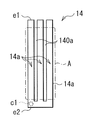
- FIG. 12A shows the configuration of the first electrode 14 according to Modification 1-1.
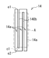
- FIG. 12B shows the configuration of the first electrode 14 according to Modification 1-2.
- FIG. 12C shows the configuration of the first electrode 14 according to Modification 1-3.
- the configuration in which the three sub electrodes 14a are arranged in a stripe shape in the first electrode 14 and the sub electrodes 14a are connected at the end portions (end portions e1 and e2) is illustrated.
- the configuration of the end of the sub-electrode 14a in the first electrode 14 is not limited to this, and can take various forms. The configuration described here is just an example.
- the three sub-electrodes 14a may be connected only at one end (here, the end portion e2).
- the first electrode 14 has a plurality (two in this case) of notches 140a. These notches 140a are open on one side of the end portions e1 and e2 (here, the end portion e1), and extend along the long side direction of the sub-electrode 14a.
- the three sub-electrodes 14a may be alternately folded (bent) at the end portions e1 and e2.
- the first electrode 14 has a plurality of (here, two) notches 140b.
- One of these notches 140b is open on the end e1 side and extends along the long side direction of the sub-electrode 14a, and the other notch 140b is opened on the end e2 side. It extends along the long side direction of 14a.
- any of these modifications 1-1 and 1-2 since the three sub-electrodes 14a are electrically connected, a voltage is applied to each sub-electrode 14a via one contact portion c1. It can be supplied.
- the sub-electrodes 14a in the first electrode 14 may be electrically separated.
- the first electrode 14 has a plurality of (here, two) gaps (gap 140c), and is thus divided into a plurality of sub-electrodes 14a.
- the contact part c1 is arrange
- the first electrode 14 only needs to include a plurality of sub-electrodes 14a in the region A that contributes to light emission, for example, and the configuration of the end portions e1 and e2 (regions other than the region A) is not particularly limited. Further, the number of divisions of the first electrode 14 in the region A (the number of sub-electrodes 14a) is not limited to three as described above, and may be two, or four or more. It doesn't matter.
- FIG. 13A shows the configuration of the first electrode 14 according to Modification 2-1.
- FIG. 13B shows the configuration of the first electrode 14 according to Modification 3-2.
- the surface shape of the sub-electrode 14a has a rectangular shape is illustrated, but the surface shape of the sub-electrode 14a is not limited to the rectangular shape, and may take various shapes.
- the configuration described here is just an example.
- each of the three sub-electrodes (sub-electrodes 14b) in the first electrode 14 may include a circular portion 14b1.
- a plurality of circular portions 14b1 are connected (electrically connected) and arranged.
- each of the three sub-electrodes 14b in the first electrode 14 may include an elliptical portion 14b2.
- a plurality of ellipsoidal portions 14b2 are connected (electrically connected) and arranged.
- the sub-electrodes 14b are electrically connected to each other in a region other than the region A of the first electrode 14, and a voltage is supplied to each sub-electrode 14b through one contact portion c1.
- the first insulating film 15 is provided with the opening H1a having the reflector 40 for each circular portion 14b1 (or for each elliptical portion 14b2). Is desirable.
- the sub-electrode 14b is not limited to the circular shape and the elliptical shape as described above, and may include a polygonal shape (n-corner shape: n is an integer of 3 or 5 or more).
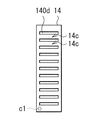
- FIG. 14A shows the configuration of the first electrode 14 according to Modification 3-1.
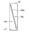
- FIG. 14B shows the configuration of the first electrode 14 according to Modification 3-2.
- the dividing direction of the first electrode 14 is not limited to this.
- the first electrode 14 may be divided along the short side direction of the rectangle.
- the first electrode 14 is provided with a plurality of slits 140d extending along the short side direction, and a plurality of sub-electrodes 14c extending in the short side direction are formed by these slits 140d.
- the first electrode 14 may be divided along the rectangular diagonal direction (oblique direction).
- the first electrode 14 is provided with a slit 140e extending along an oblique direction, and the two sub-electrodes 14d are formed by the slit 140e.
- FIG. 15 illustrates a configuration of the first electrode 14 according to the fourth modification.
- the surface shape of the 1st electrode 14 illustrated the structure which has a rectangular shape
- the surface shape of the 1st electrode 14 is not limited to a rectangular shape.
- the square first electrode 14 may be used.
- the same effect as in the above embodiment can be obtained by arranging a plurality (here, five) of sub-electrodes 14a through the slit 140, as in the above embodiment.
- FIG. 16 illustrates a configuration of a pixel portion according to the fifth modification.
- the configuration in which the organic layer 16 of the organic EL element 10 generates white light for example, a configuration assuming a dry process such as a vacuum deposition method
- the configuration of the pixel portion (organic layer) is this. It is not limited to.
- the organic layers (organic layers 16R, 16G, and 16B) of each color may be formed by, for example, a wet process (printing and coating).
- the pixel isolation film 15 has a stacked structure of a first insulating film 15A and a second insulating film 15B, and functions as a partition wall.
- FIG. 17 shows a functional block configuration of an electronic device (electronic device 1A) to which the display device 1 is applied.
- the electronic device 1A include a television device, a personal computer (PC), a smartphone, a tablet PC, a mobile phone, a digital still camera, a digital video camera, and the like.
- the electronic apparatus 1A includes, for example, the display device 1 and the interface unit 30 described above.
- the interface unit 30 is an input unit to which various signals, a power source, and the like are input from the outside.
- the interface unit 30 may also include a user interface such as a touch panel, a keyboard, or operation buttons.
- the present disclosure has been described with reference to the embodiment, the present disclosure is not limited to the above-described embodiment, and various modifications can be made.
- the reflector 40 of the opening H1a uses the difference in refractive index between the first insulating film 15 and the second insulating film 18, but the side surface of the opening H1a ( A reflective structure can be formed by providing a metal film or the like on the inclined surface PS).
- each layer described in the above embodiments and the like, or the film formation method and film formation conditions are not limited, and may be other materials and thicknesses, or other film formation methods and Film forming conditions may be used.
- the configuration of the organic EL element 10 is specifically described. However, it is not necessary to provide all the layers, and other layers may be further provided.
- the present disclosure can also be applied to a passive matrix display device.
- the configuration of the pixel circuit PXLC for active matrix driving is not limited to that described in the above embodiment, and a capacitor or a transistor may be added as necessary.
- a necessary driving circuit may be added in addition to the scanning line driving unit 3, the signal line driving unit 4, and the power line driving unit 5 described above in accordance with the change of the pixel circuit PXLC.
- Each of the plurality of pixels is A first electrode including a plurality of sub-electrodes; An insulating film formed on the first electrode and having an opening facing each of the plurality of sub-electrodes; An organic layer formed in each opening of the insulating film and including a light emitting layer; And a second electrode formed on the organic layer.
- each surface shape of the plurality of sub-electrodes has a rectangular shape.
- the plurality of sub-electrodes have a stripe shape as a whole.
- each of the plurality of sub-electrodes has a plurality of circular portions or polygonal portions.
- Each of the plurality of pixels is A first electrode including a plurality of sub-electrodes; An insulating film formed on the first electrode and having an opening facing each of the plurality of sub-electrodes; An organic layer formed in each opening of the insulating film and including a light emitting layer; An electronic apparatus comprising: a display device comprising: a second electrode formed on the organic layer.
Landscapes
- Physics & Mathematics (AREA)
- Optics & Photonics (AREA)
- Engineering & Computer Science (AREA)
- Microelectronics & Electronic Packaging (AREA)
- Manufacturing & Machinery (AREA)
- Electroluminescent Light Sources (AREA)
Abstract
La présente invention concerne un dispositif d'affichage qui est pourvu d'une pluralité de pixels. Chaque pixel de la pluralité de pixels comprend une première électrode, un film isolant formé sur la première électrode et comportant une pluralité d'ouvertures, une couche organique formée sur les ouvertures dans le film isolant et comprenant une couche électroluminescente, et une seconde électrode formée sur la couche organique. La première électrode comporte une pluralité de sous-électrodes disposées de sorte à faire chacune face à chaque ouverture dans le film isolant.
Priority Applications (3)
| Application Number | Priority Date | Filing Date | Title |
|---|---|---|---|
| CN201780027476.6A CN109315049B (zh) | 2016-05-11 | 2017-04-20 | 显示装置和电子设备 |
| JP2018516919A JP6640336B2 (ja) | 2016-05-11 | 2017-04-20 | 表示装置および電子機器 |
| US16/183,663 US11201309B2 (en) | 2016-05-11 | 2018-11-07 | Display unit and electronic apparatus including a divided electrode |
Applications Claiming Priority (2)
| Application Number | Priority Date | Filing Date | Title |
|---|---|---|---|
| JP2016-095343 | 2016-05-11 | ||
| JP2016095343 | 2016-05-11 |
Related Child Applications (1)
| Application Number | Title | Priority Date | Filing Date |
|---|---|---|---|
| US16/183,663 Continuation US11201309B2 (en) | 2016-05-11 | 2018-11-07 | Display unit and electronic apparatus including a divided electrode |
Publications (1)
| Publication Number | Publication Date |
|---|---|
| WO2017195560A1 true WO2017195560A1 (fr) | 2017-11-16 |
Family
ID=60266534
Family Applications (1)
| Application Number | Title | Priority Date | Filing Date |
|---|---|---|---|
| PCT/JP2017/015896 Ceased WO2017195560A1 (fr) | 2016-05-11 | 2017-04-20 | Dispositif d'affichage et dispositif électronique |
Country Status (4)
| Country | Link |
|---|---|
| US (1) | US11201309B2 (fr) |
| JP (1) | JP6640336B2 (fr) |
| CN (1) | CN109315049B (fr) |
| WO (1) | WO2017195560A1 (fr) |
Cited By (7)
| Publication number | Priority date | Publication date | Assignee | Title |
|---|---|---|---|---|
| CN110767830A (zh) * | 2018-12-28 | 2020-02-07 | 云谷(固安)科技有限公司 | 透明oled基板、阵列基板、显示屏及显示装置 |
| CN110767831A (zh) * | 2018-12-28 | 2020-02-07 | 昆山国显光电有限公司 | 透明oled基板、显示面板、阵列基板、显示屏及显示装置 |
| CN110767106A (zh) * | 2018-09-30 | 2020-02-07 | 云谷(固安)科技有限公司 | 显示面板、显示屏及显示终端 |
| CN110767835A (zh) * | 2019-03-29 | 2020-02-07 | 昆山国显光电有限公司 | 透明显示面板、显示屏、显示装置及掩膜板 |
| WO2020029559A1 (fr) * | 2018-08-06 | 2020-02-13 | 云谷(固安)科技有限公司 | Panneau d'affichage, écran d'affichage et terminal d'affichage |
| US10720597B2 (en) * | 2017-08-31 | 2020-07-21 | Lg Display Co., Ltd. | Electroluminescent display device |
| WO2021005438A1 (fr) * | 2019-07-05 | 2021-01-14 | 株式会社半導体エネルギー研究所 | Dispositif électroluminescent, panneau de commande, dispositif d'affichage, dispositif d'entrée/sortie et dispositif de traitement d'informations |
Families Citing this family (8)
| Publication number | Priority date | Publication date | Assignee | Title |
|---|---|---|---|---|
| JPWO2017204150A1 (ja) * | 2016-05-24 | 2019-03-14 | 株式会社Joled | 有機el表示パネル、有機el表示装置、及び、その製造方法 |
| CN110767713A (zh) * | 2019-03-08 | 2020-02-07 | 云谷(固安)科技有限公司 | 显示装置及其oled基板、oled透光基板 |
| CN109873023B (zh) * | 2019-03-29 | 2021-10-19 | 京东方科技集团股份有限公司 | 一种oled显示基板及其制备方法、显示装置 |
| CN110767139B (zh) * | 2019-03-29 | 2020-12-11 | 昆山国显光电有限公司 | 显示基板、显示面板及显示装置 |
| CN110767085B (zh) * | 2019-03-29 | 2021-11-30 | 昆山国显光电有限公司 | 显示基板、显示面板及显示装置 |
| CN111180483B (zh) * | 2019-04-04 | 2021-02-26 | 昆山国显光电有限公司 | Oled阵列基板、显示面板及显示装置 |
| CN112420962A (zh) * | 2020-12-02 | 2021-02-26 | 深圳市华星光电半导体显示技术有限公司 | 显示面板及其制作方法 |
| CN114335368B (zh) * | 2021-12-24 | 2024-04-19 | 北京京东方技术开发有限公司 | 发光器件及其制作方法、显示装置 |
Citations (7)
| Publication number | Priority date | Publication date | Assignee | Title |
|---|---|---|---|---|
| JP2003243182A (ja) * | 2002-02-19 | 2003-08-29 | Sanyo Electric Co Ltd | 有機el素子 |
| JP2006260792A (ja) * | 2005-03-15 | 2006-09-28 | Seiko Epson Corp | 有機el装置、電子機器 |
| JP2006294364A (ja) * | 2005-04-08 | 2006-10-26 | Seiko Epson Corp | 有機エレクトロルミネッセンス装置の製造方法、有機エレクトロルミネッセンス装置、電子機器 |
| JP2009288735A (ja) * | 2008-06-02 | 2009-12-10 | Sony Corp | 画像表示装置及び画像表示装置の製造方法 |
| JP2011034849A (ja) * | 2009-08-03 | 2011-02-17 | Toshiba Mobile Display Co Ltd | 有機el装置 |
| JP2014207105A (ja) * | 2013-04-11 | 2014-10-30 | ソニー株式会社 | 表示装置および電子機器 |
| JP2015144087A (ja) * | 2014-01-31 | 2015-08-06 | ソニー株式会社 | 有機電界発光装置および電子機器 |
Family Cites Families (20)
| Publication number | Priority date | Publication date | Assignee | Title |
|---|---|---|---|---|
| US6339289B1 (en) * | 1998-07-24 | 2002-01-15 | Xerox Corporation | Method and apparatus to limit dark spot propagation in organic light emitting diodes |
| US6933673B2 (en) * | 2001-04-27 | 2005-08-23 | Semiconductor Energy Laboratory Co., Ltd. | Luminescent device and process of manufacturing the same |
| CN1505167A (zh) * | 2002-11-28 | 2004-06-16 | 友达光电股份有限公司 | 修补主动式有机发光二极管的方法 |
| US7030553B2 (en) * | 2003-08-19 | 2006-04-18 | Eastman Kodak Company | OLED device having microcavity gamut subpixels and a within gamut subpixel |
| JP4165478B2 (ja) * | 2003-11-07 | 2008-10-15 | セイコーエプソン株式会社 | 発光装置及び電子機器 |
| KR101066411B1 (ko) * | 2004-03-31 | 2011-09-21 | 삼성전자주식회사 | 표시장치 및 이의 제조 방법 |
| US7057339B2 (en) * | 2004-04-08 | 2006-06-06 | Eastman Kodak Company | OLED with color change media |
| KR100721948B1 (ko) | 2005-08-30 | 2007-05-25 | 삼성에스디아이 주식회사 | 유기 전계 발광 표시 장치 및 그의 제조 방법 |
| KR100713998B1 (ko) * | 2005-09-30 | 2007-05-04 | 삼성에스디아이 주식회사 | 분할 구조 전극을 가지는 유기 발광 표시장치 및 이의 보수방법 |
| TW200803606A (en) * | 2006-06-13 | 2008-01-01 | Itc Inc Ltd | The fabrication of full color OLED panel using micro-cavity structure |
| JP5061562B2 (ja) * | 2006-09-29 | 2012-10-31 | セイコーエプソン株式会社 | 発光装置及び電子機器 |
| KR101002663B1 (ko) * | 2008-12-11 | 2010-12-21 | 삼성모바일디스플레이주식회사 | 유기 발광 표시 장치 |
| JP2010257957A (ja) * | 2009-04-01 | 2010-11-11 | Seiko Epson Corp | 有機エレクトロルミネッセンス装置 |
| JP2014225329A (ja) * | 2011-09-12 | 2014-12-04 | シャープ株式会社 | 発光デバイス、表示装置、及び照明装置 |
| WO2013038971A1 (fr) * | 2011-09-12 | 2013-03-21 | シャープ株式会社 | Dispositif électroluminescent, dispositif d'affichage et dispositif d'éclairage |
| KR101801913B1 (ko) * | 2012-03-23 | 2017-11-28 | 삼성디스플레이 주식회사 | 유기 발광 디스플레이 장치와, 이의 제조 방법 |
| KR101939366B1 (ko) * | 2012-09-11 | 2019-01-17 | 삼성디스플레이 주식회사 | 유기 발광 표시 장치 |
| US9401180B2 (en) * | 2012-10-12 | 2016-07-26 | International Business Machines Corporation | High resolution tape directory (HRTD) stored at end of data in an index partition |
| KR102173041B1 (ko) * | 2013-05-23 | 2020-11-03 | 삼성디스플레이 주식회사 | 유기 발광 표시 장치 및 그 제조 방법 |
| CN103616786B (zh) * | 2013-12-10 | 2017-01-04 | 华映视讯(吴江)有限公司 | 薄膜晶体管基板及其修护方法 |
-
2017
- 2017-04-20 CN CN201780027476.6A patent/CN109315049B/zh active Active
- 2017-04-20 JP JP2018516919A patent/JP6640336B2/ja active Active
- 2017-04-20 WO PCT/JP2017/015896 patent/WO2017195560A1/fr not_active Ceased
-
2018
- 2018-11-07 US US16/183,663 patent/US11201309B2/en active Active
Patent Citations (7)
| Publication number | Priority date | Publication date | Assignee | Title |
|---|---|---|---|---|
| JP2003243182A (ja) * | 2002-02-19 | 2003-08-29 | Sanyo Electric Co Ltd | 有機el素子 |
| JP2006260792A (ja) * | 2005-03-15 | 2006-09-28 | Seiko Epson Corp | 有機el装置、電子機器 |
| JP2006294364A (ja) * | 2005-04-08 | 2006-10-26 | Seiko Epson Corp | 有機エレクトロルミネッセンス装置の製造方法、有機エレクトロルミネッセンス装置、電子機器 |
| JP2009288735A (ja) * | 2008-06-02 | 2009-12-10 | Sony Corp | 画像表示装置及び画像表示装置の製造方法 |
| JP2011034849A (ja) * | 2009-08-03 | 2011-02-17 | Toshiba Mobile Display Co Ltd | 有機el装置 |
| JP2014207105A (ja) * | 2013-04-11 | 2014-10-30 | ソニー株式会社 | 表示装置および電子機器 |
| JP2015144087A (ja) * | 2014-01-31 | 2015-08-06 | ソニー株式会社 | 有機電界発光装置および電子機器 |
Cited By (19)
| Publication number | Priority date | Publication date | Assignee | Title |
|---|---|---|---|---|
| US10720597B2 (en) * | 2017-08-31 | 2020-07-21 | Lg Display Co., Ltd. | Electroluminescent display device |
| JP2021507289A (ja) * | 2018-08-06 | 2021-02-22 | ユング(グアン)テクノロジー カンパニー リミテッド | 表示パネル、ディスプレイ及び表示端末 |
| KR102489280B1 (ko) * | 2018-08-06 | 2023-01-17 | 윤구(구안) 테크놀로지 컴퍼니 리미티드 | 디스플레이 패널, 디스플레이 스크린 및 디스플레이 단말기 |
| JP7125485B2 (ja) | 2018-08-06 | 2022-08-24 | ユング(グアン)テクノロジー カンパニー リミテッド | 表示パネル、ディスプレイ及び表示端末 |
| US11244992B2 (en) | 2018-08-06 | 2022-02-08 | Yungu (Gu'an) Technology Co., Ltd. | Display panels, display screens, and display terminals |
| WO2020029559A1 (fr) * | 2018-08-06 | 2020-02-13 | 云谷(固安)科技有限公司 | Panneau d'affichage, écran d'affichage et terminal d'affichage |
| KR20200083620A (ko) * | 2018-08-06 | 2020-07-08 | 윤구(구안) 테크놀로지 컴퍼니 리미티드 | 디스플레이 패널, 디스플레이 스크린 및 디스플레이 단말기 |
| US11263964B2 (en) | 2018-09-30 | 2022-03-01 | Yungu (Gu'an) Technology Co., Ltd. | Display panel, display screen, and display terminal |
| CN110767106B (zh) * | 2018-09-30 | 2020-09-08 | 云谷(固安)科技有限公司 | 显示面板、显示屏及显示终端 |
| CN110767106A (zh) * | 2018-09-30 | 2020-02-07 | 云谷(固安)科技有限公司 | 显示面板、显示屏及显示终端 |
| CN110767830A (zh) * | 2018-12-28 | 2020-02-07 | 云谷(固安)科技有限公司 | 透明oled基板、阵列基板、显示屏及显示装置 |
| CN110767831A (zh) * | 2018-12-28 | 2020-02-07 | 昆山国显光电有限公司 | 透明oled基板、显示面板、阵列基板、显示屏及显示装置 |
| CN110767835A (zh) * | 2019-03-29 | 2020-02-07 | 昆山国显光电有限公司 | 透明显示面板、显示屏、显示装置及掩膜板 |
| US11895859B2 (en) | 2019-03-29 | 2024-02-06 | Kunshan Go-Visionox Opto-Electronics Co., Ltd. | Transparent display panels, display screens, and mask plates |
| WO2021005438A1 (fr) * | 2019-07-05 | 2021-01-14 | 株式会社半導体エネルギー研究所 | Dispositif électroluminescent, panneau de commande, dispositif d'affichage, dispositif d'entrée/sortie et dispositif de traitement d'informations |
| JPWO2021005438A1 (fr) * | 2019-07-05 | 2021-01-14 | ||
| JP7474256B2 (ja) | 2019-07-05 | 2024-04-24 | 株式会社半導体エネルギー研究所 | 発光デバイス、機能パネル、表示装置、入出力装置、情報処理装置 |
| JP2024086883A (ja) * | 2019-07-05 | 2024-06-28 | 株式会社半導体エネルギー研究所 | 発光デバイス |
| US12389745B2 (en) | 2019-07-05 | 2025-08-12 | Semiconductor Energy Laboratory Co., Ltd. | Light-emitting device configured to improve light-extraction efficiency including reflective structure body between first electrode and light-emitting material, functional panel, display device, input/output device, and data processing device |
Also Published As
| Publication number | Publication date |
|---|---|
| JPWO2017195560A1 (ja) | 2018-08-02 |
| CN109315049A (zh) | 2019-02-05 |
| US20190074471A1 (en) | 2019-03-07 |
| US11201309B2 (en) | 2021-12-14 |
| JP6640336B2 (ja) | 2020-02-05 |
| CN109315049B (zh) | 2021-10-08 |
Similar Documents
| Publication | Publication Date | Title |
|---|---|---|
| JP6640336B2 (ja) | 表示装置および電子機器 | |
| CN107664862B (zh) | 显示装置及其制造方法 | |
| US9478742B2 (en) | Electroluminescence device and manufacturing method thereof | |
| US9178180B2 (en) | Display device and electronic apparatus | |
| CN106340250A (zh) | 显示面板 | |
| KR20200093718A (ko) | 유기 발광 표시 장치 및 유기 발광 표시 장치의 제조 방법 | |
| US20090251048A1 (en) | Organic light emitting device and manufacturing method thereof | |
| US10665820B2 (en) | Display device | |
| JP6223070B2 (ja) | 有機el表示装置及び有機el表示装置の製造方法 | |
| TWI835233B (zh) | 具有氧化物半導體的顯示設備 | |
| JP2019016429A (ja) | 表示装置および表示装置の製造方法 | |
| KR20180132935A (ko) | 표시 장치 및 전자 기기 | |
| JP6872244B2 (ja) | 表示装置 | |
| KR102248489B1 (ko) | 표시 장치 및 전자 기기 | |
| KR20160013443A (ko) | 칼라 필터를 구비한 하부 발광형 유기발광 다이오드 표시장치 및 그 제조 방법 | |
| US20250194338A1 (en) | Display panel including a first conductive member in a first area and a second conductive member in a second area | |
| CN113130578B (zh) | 显示装置及其制造方法 | |
| US20250221186A1 (en) | Display Device | |
| CN120568814A (zh) | 晶体管和包括该晶体管的显示设备 | |
| US12490631B2 (en) | Light emitting display device | |
| US20230411440A1 (en) | Display device | |
| JP2019053172A (ja) | 表示装置 | |
| US20230276664A1 (en) | Display device | |
| JP6040553B2 (ja) | 発光デバイス、発光デバイスの製造方法及び電子機器 | |
| JP2006284915A (ja) | 表示装置及びアレイ基板 |
Legal Events
| Date | Code | Title | Description |
|---|---|---|---|
| ENP | Entry into the national phase |
Ref document number: 2018516919 Country of ref document: JP Kind code of ref document: A |
|
| NENP | Non-entry into the national phase |
Ref country code: DE |
|
| 121 | Ep: the epo has been informed by wipo that ep was designated in this application |
Ref document number: 17795921 Country of ref document: EP Kind code of ref document: A1 |
|
| 122 | Ep: pct application non-entry in european phase |
Ref document number: 17795921 Country of ref document: EP Kind code of ref document: A1 |