WO2017199649A1 - Circuit frontal à haute fréquence et dispositif de communication - Google Patents
Circuit frontal à haute fréquence et dispositif de communication Download PDFInfo
- Publication number
- WO2017199649A1 WO2017199649A1 PCT/JP2017/014956 JP2017014956W WO2017199649A1 WO 2017199649 A1 WO2017199649 A1 WO 2017199649A1 JP 2017014956 W JP2017014956 W JP 2017014956W WO 2017199649 A1 WO2017199649 A1 WO 2017199649A1
- Authority
- WO
- WIPO (PCT)
- Prior art keywords
- band
- terminal
- filter
- reception
- frequency front
- Prior art date
- Legal status (The legal status is an assumption and is not a legal conclusion. Google has not performed a legal analysis and makes no representation as to the accuracy of the status listed.)
- Ceased
Links
Images






Classifications
-
- H—ELECTRICITY
- H04—ELECTRIC COMMUNICATION TECHNIQUE
- H04B—TRANSMISSION
- H04B1/00—Details of transmission systems, not covered by a single one of groups H04B3/00 - H04B13/00; Details of transmission systems not characterised by the medium used for transmission
- H04B1/38—Transceivers, i.e. devices in which transmitter and receiver form a structural unit and in which at least one part is used for functions of transmitting and receiving
- H04B1/40—Circuits
- H04B1/44—Transmit/receive switching
-
- H—ELECTRICITY
- H03—ELECTRONIC CIRCUITRY
- H03F—AMPLIFIERS
- H03F3/00—Amplifiers with only discharge tubes or only semiconductor devices as amplifying elements
- H03F3/189—High-frequency amplifiers, e.g. radio frequency amplifiers
- H03F3/19—High-frequency amplifiers, e.g. radio frequency amplifiers with semiconductor devices only
-
- H—ELECTRICITY
- H03—ELECTRONIC CIRCUITRY
- H03F—AMPLIFIERS
- H03F3/00—Amplifiers with only discharge tubes or only semiconductor devices as amplifying elements
- H03F3/20—Power amplifiers, e.g. Class B amplifiers, Class C amplifiers
- H03F3/24—Power amplifiers, e.g. Class B amplifiers, Class C amplifiers of transmitter output stages
- H03F3/245—Power amplifiers, e.g. Class B amplifiers, Class C amplifiers of transmitter output stages with semiconductor devices only
-
- H—ELECTRICITY
- H03—ELECTRONIC CIRCUITRY
- H03H—IMPEDANCE NETWORKS, e.g. RESONANT CIRCUITS; RESONATORS
- H03H9/00—Networks comprising electromechanical or electro-acoustic elements; Electromechanical resonators
- H03H9/70—Multiple-port networks for connecting several sources or loads, working on different frequencies or frequency bands, to a common load or source
- H03H9/72—Networks using surface acoustic waves
-
- H—ELECTRICITY
- H04—ELECTRIC COMMUNICATION TECHNIQUE
- H04B—TRANSMISSION
- H04B1/00—Details of transmission systems, not covered by a single one of groups H04B3/00 - H04B13/00; Details of transmission systems not characterised by the medium used for transmission
-
- H—ELECTRICITY
- H04—ELECTRIC COMMUNICATION TECHNIQUE
- H04B—TRANSMISSION
- H04B1/00—Details of transmission systems, not covered by a single one of groups H04B3/00 - H04B13/00; Details of transmission systems not characterised by the medium used for transmission
- H04B1/005—Details of transmission systems, not covered by a single one of groups H04B3/00 - H04B13/00; Details of transmission systems not characterised by the medium used for transmission adapting radio receivers, transmitters andtransceivers for operation on two or more bands, i.e. frequency ranges
- H04B1/0053—Details of transmission systems, not covered by a single one of groups H04B3/00 - H04B13/00; Details of transmission systems not characterised by the medium used for transmission adapting radio receivers, transmitters andtransceivers for operation on two or more bands, i.e. frequency ranges with common antenna for more than one band
- H04B1/0057—Details of transmission systems, not covered by a single one of groups H04B3/00 - H04B13/00; Details of transmission systems not characterised by the medium used for transmission adapting radio receivers, transmitters andtransceivers for operation on two or more bands, i.e. frequency ranges with common antenna for more than one band using diplexing or multiplexing filters for selecting the desired band
-
- H—ELECTRICITY
- H04—ELECTRIC COMMUNICATION TECHNIQUE
- H04B—TRANSMISSION
- H04B1/00—Details of transmission systems, not covered by a single one of groups H04B3/00 - H04B13/00; Details of transmission systems not characterised by the medium used for transmission
- H04B1/38—Transceivers, i.e. devices in which transmitter and receiver form a structural unit and in which at least one part is used for functions of transmitting and receiving
- H04B1/40—Circuits
- H04B1/50—Circuits using different frequencies for the two directions of communication
-
- H—ELECTRICITY
- H03—ELECTRONIC CIRCUITRY
- H03F—AMPLIFIERS
- H03F2200/00—Indexing scheme relating to amplifiers
- H03F2200/171—A filter circuit coupled to the output of an amplifier
-
- H—ELECTRICITY
- H03—ELECTRONIC CIRCUITRY
- H03F—AMPLIFIERS
- H03F2200/00—Indexing scheme relating to amplifiers
- H03F2200/294—Indexing scheme relating to amplifiers the amplifier being a low noise amplifier [LNA]
-
- H—ELECTRICITY
- H03—ELECTRONIC CIRCUITRY
- H03F—AMPLIFIERS
- H03F2200/00—Indexing scheme relating to amplifiers
- H03F2200/451—Indexing scheme relating to amplifiers the amplifier being a radio frequency amplifier
-
- H—ELECTRICITY
- H03—ELECTRONIC CIRCUITRY
- H03H—IMPEDANCE NETWORKS, e.g. RESONANT CIRCUITS; RESONATORS
- H03H9/00—Networks comprising electromechanical or electro-acoustic elements; Electromechanical resonators
- H03H9/46—Filters
- H03H9/64—Filters using surface acoustic waves
- H03H9/6423—Means for obtaining a particular transfer characteristic
- H03H9/6433—Coupled resonator filters
- H03H9/6436—Coupled resonator filters having one acoustic track only
-
- H—ELECTRICITY
- H03—ELECTRONIC CIRCUITRY
- H03H—IMPEDANCE NETWORKS, e.g. RESONANT CIRCUITS; RESONATORS
- H03H9/00—Networks comprising electromechanical or electro-acoustic elements; Electromechanical resonators
- H03H9/46—Filters
- H03H9/64—Filters using surface acoustic waves
- H03H9/6423—Means for obtaining a particular transfer characteristic
- H03H9/6433—Coupled resonator filters
- H03H9/6483—Ladder SAW filters
-
- H—ELECTRICITY
- H03—ELECTRONIC CIRCUITRY
- H03H—IMPEDANCE NETWORKS, e.g. RESONANT CIRCUITS; RESONATORS
- H03H9/00—Networks comprising electromechanical or electro-acoustic elements; Electromechanical resonators
- H03H9/70—Multiple-port networks for connecting several sources or loads, working on different frequencies or frequency bands, to a common load or source
- H03H9/72—Networks using surface acoustic waves
- H03H9/725—Duplexers
Definitions
- the present invention relates to a high-frequency front-end circuit and a communication device.
- FIG. 14 is a circuit configuration diagram of a multiband compatible mobile communication terminal capable of carrier aggregation described in Patent Document 1.
- the mobile communication terminal shown in the figure includes an antenna 611, a tunable diplexer 600, SPDT switches 612 and 613, duplexers 614, 615A, 615B and 616, a low noise amplifier 630, a power amplifier 631, an RF signal processing circuit 632, and a base.
- a band signal processing circuit 633 is provided.
- the tunable diplexer 600 includes an inductor and a variable capacitance element. SPDT switches 612 and 613 select an arbitrary duplexer and vary the frequency characteristics of tunable diplexer 600. According to the above configuration, it is possible to realize the carrier aggregation of Band 21 and Band 3 and the carrier aggregation of Band 21 and Band 19.
- the present invention has been made to solve the above-described problems, and is a high-frequency front end that can be reduced in size and price by reducing the number of filters or duplexers in a multi-band compatible system.
- An object is to provide a circuit and a communication device.
- a high-frequency front-end circuit is a high-frequency front-end circuit that has a common antenna terminal connected to an antenna element and transmits and receives a high-frequency signal through the antenna element.
- a first input / output terminal and a second input / output terminal wherein the first input / output terminal is connected to the antenna common terminal, and at least a pass band is changed to a first pass band or a second pass band.
- a second filter having three passbands, a first common terminal, a first selection terminal, and a second selection terminal, wherein the first common terminal is connected to the second input / output terminal.
- the first selection terminal is connected to one of the transmission path and the reception path
- the second selection terminal is connected to the other of the transmission path and the reception path, the first common terminal and the first selection terminal
- a first switch circuit that exclusively switches the connection between the first common terminal and the second selection terminal.
- the first filter can be switched to the transmission filter and the reception filter by the first switch circuit. For this reason, for example, even when the transmission band and the reception band of different bands are partially overlapped or close to each other, the first filter receives the transmission filter for one band and the reception for the other band. It can also be used as a filter. Thereby, in the system corresponding to a multiband, the number of filters or a duplexer composed of the filters can be reduced. Furthermore, the number of switch terminals for band switching can be reduced. Therefore, the high-frequency front end circuit can be reduced in size and price.
- a transmission terminal connected to the transmission side path for inputting a high frequency signal from a subsequent circuit
- a reception terminal connected to the reception side path for outputting the high frequency signal to the subsequent circuit
- a second common terminal And a third selection terminal and a fourth selection terminal, wherein the third selection terminal is connected to the second selection terminal, the fourth selection terminal is connected to the fourth input / output terminal, and the second common And a second switch circuit connected to one of the reception terminal and the transmission terminal, and the first selection terminal may be connected to the other of the reception terminal and the transmission terminal.
- the second filter when the first switch is used as a transmission filter by the second switch circuit, for example, the second filter can be used as a reception filter.
- the first filter when used as a reception filter, the second filter can be used as a transmission filter.
- the first switch circuit may be a single pole double throw switch.
- the switch circuit can have a simplified single-pole double-throw switch configuration. As a result, the entire high-frequency front-end circuit can be reduced in size and price.
- first switch circuit and the second switch circuit may be formed in one package.
- the second selection terminal and the third selection terminal are made common, two common terminals (first common terminal and second common terminal) and three selection terminals (first selection terminal to fourth selection terminal).
- the first switch circuit and the second switch circuit can be integrated. Therefore, the high-frequency front end circuit can be reduced in size and price.
- the high-frequency front-end circuit is exclusive of the first band having the first pass band as a transmission band and the third pass band as a reception band, and the second band as a reception band.
- the first pass band and the second pass band may overlap at least partially.
- the high-frequency front-end circuit includes the first band, Band 28b (transmission band: 718-748 MHz, reception band: 773-803 MHz) of LTE (Long Term Evolution) standard, and Band 29 (reception band: 717.
- the high frequency signal of the second band which is 25-727.25 MHz) and the third band which is Band 28a of LTE standard may be transmitted and received.
- the first filter By switching the pass band of the first filter to the first pass band and the second pass band, the first filter can be applied to the Band 28a and Band 28b transmission filters. Furthermore, the first switch circuit can apply the first filter to the Band 29 reception filter. Therefore, the multiband high-frequency front-end circuit having the three bands can be configured with a small size and at a low price.
- the high-frequency front end circuit includes the first band, which is LTE band 27 (transmission band: 807-824 MHz, reception band: 852-869 MHz), and the LTE band 20 (transmission band: 832-862 MHz, reception band: 792-821 MHz), the second band high-frequency signal may be transmitted and received.
- LTE band 27 transmission band: 807-824 MHz, reception band: 852-869 MHz
- LTE band 20 transmission band: 832-862 MHz, reception band: 792-821 MHz
- the second band high-frequency signal may be transmitted and received.
- the first filter can be applied to the Band 27 transmission filter and the Band 20 reception filter by switching the pass band of the first filter to the first pass band and the second pass band. Therefore, the multiband high-frequency front-end circuit having the two bands can be configured in a small size and at a low price.
- the first filter includes a series arm resonator connected between the first input / output terminal and the second input / output terminal, the first input / output terminal, the series arm resonator, and the first filter.
- a parallel arm resonator connected between a node on a path connecting two input / output terminals and a reference terminal; and between the node and the reference terminal, the node, the parallel arm resonator, and the And a switch element that switches between conduction and non-conduction of a path connecting the reference terminals.
- the band-pass filter circuit including the series arm resonator and the parallel arm resonator
- the switch element when the switch element is in a non-conduction state, the series arm resonator and the parallel arm resonator are Thus, the first band pass characteristic is formed.
- a different circuit state is formed between the node and the reference terminal, so that a second band pass characteristic different from the first band pass characteristic is formed.
- a tunable filter circuit applied to a system that exclusively selects two bands close to each other requires two filter circuits and an SPDT type switch that switches between the two filters.
- this configuration can be configured with one filter circuit and an SPST (Single Pole Single Throw) type switch element. Therefore, the variable first filter can be simplified and downsized.
- first filter and the second filter may be any one of a surface acoustic wave filter, an elastic wave filter using a BAW (Bulk Acoustic Wave), an LC resonance filter, and a dielectric filter.
- BAW Bit Acoustic Wave
- the switch element may be a FET (Field Effect Transistor) switch made of GaAs or CMOS (Complementary Metal Oxide Semiconductor), or a diode switch.
- FET Field Effect Transistor
- CMOS Complementary Metal Oxide Semiconductor
- a transmission amplification circuit that is connected to the transmission side path and amplifies a high frequency transmission signal
- a reception amplification circuit that is connected to the reception side path and amplifies the high frequency reception signal
- a communication apparatus processes the high-frequency signal, the high-frequency front-end circuit described above, a control unit that controls the passband of the first filter and the connection state of the first switch circuit, and An RF signal processing circuit, wherein the control unit switches between the first passband and the second passband and connects the first common terminal with the first selection terminal and the second selection terminal. Link the switching.
- control unit controls the connection state of the first switch circuit and the pass band of the first filter, a communication device capable of accurately selecting a filter corresponding to the multi-band can be realized.
- the number of filters or duplexers and the number of switch terminals for band switching can be reduced in a multi-band compatible system, so that downsizing and cost reduction are possible. It becomes.
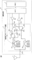
- FIG. 1 is a configuration diagram of a high-frequency front end circuit and its peripheral circuits according to the first embodiment.
- FIG. 2 is a diagram for explaining frequency allocation of bands used in the high-frequency front-end circuit according to the first embodiment.
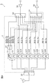
- FIG. 3 is a circuit configuration diagram of a filter constituting the high-frequency front-end circuit according to the first embodiment.
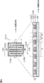
- FIG. 4 is an example of a plan view and a cross-sectional view schematically showing the resonator of the filter according to the first embodiment.
- FIG. 5A is a graph showing filter pass characteristics when the Band 28a and Band 28b are transmitted by the high-frequency front-end circuit according to the first embodiment.
- FIG. 1 is a configuration diagram of a high-frequency front end circuit and its peripheral circuits according to the first embodiment.
- FIG. 2 is a diagram for explaining frequency allocation of bands used in the high-frequency front-end circuit according to the first embodiment.
- FIG. 3 is a circuit configuration diagram of a filter constituting the high-frequency front-end circuit
- FIG. 5B is a graph illustrating filter pass characteristics when the Band 28a, Band 28b, and Band 29 are received by the high-frequency front-end circuit according to the first embodiment.
- FIG. 6 is a circuit configuration diagram of a high-frequency front end circuit according to a comparative example.
- FIG. 7 is a configuration diagram of the high-frequency front-end circuit and its peripheral circuits according to the first modification of the first embodiment.
- FIG. 8 is a configuration diagram of the high-frequency front-end circuit and its peripheral circuits according to the second modification of the first embodiment.
- FIG. 9 is a configuration diagram of a high-frequency front-end circuit and its peripheral circuits according to the third modification of the first embodiment.
- FIG. 10 is a configuration diagram of the high-frequency front-end circuit and its peripheral circuits according to the fourth modification of the first embodiment.
- FIG. 11 is a configuration diagram of the high-frequency front-end circuit and its peripheral circuits according to the second embodiment.
- FIG. 12 is a diagram for explaining frequency allocation of bands used in the high-frequency front-end circuit according to the second embodiment.
- FIG. 13A is a graph showing circuit connections during transmission / reception of Band 27 of the high-frequency front-end circuit according to the second embodiment.
- FIG. 13B is a graph showing circuit connections at the time of Band20 transmission / reception of the high-frequency front-end circuit according to the second embodiment.
- FIG. 14 is a circuit configuration diagram of a multiband-compatible mobile communication terminal capable of carrier aggregation described in Patent Document 1.
- FIG. 1 is a configuration diagram of a high-frequency front-end circuit 2 and its peripheral circuits according to the first embodiment.
- the figure shows an antenna element 1, a high-frequency front end circuit 2, a transmission amplifier circuit 3A, a reception amplifier circuit 3B, an RF signal processing circuit (RFIC) 4, and a baseband signal processing circuit (BBIC) 7. It is shown.
- the high-frequency front-end circuit 2, the transmission amplifier circuit 3A, the reception amplifier circuit 3B, the RF signal processing circuit (RFIC) 4, and the baseband signal processing circuit (BBIC) 7 constitute a communication device 9.
- the antenna element 1, the high-frequency front end circuit 2, the transmission amplifier circuit 3A, the reception amplifier circuit 3B, and the RFIC 4 are disposed, for example, in the front end portion of a mobile phone that supports multimode / multiband.
- An RFIC (Radio Frequency Integrated Circuit) 4 processes a high-frequency reception signal input from the antenna element 1 via a reception-side signal path by down-conversion or the like, and the reception signal generated by the signal processing is sent to the BBIC 7 Output. Further, the RFIC 4 performs signal processing on the transmission signal input from the BBIC 7 by up-conversion or the like, and outputs a high-frequency transmission signal generated by the signal processing to the transmission amplifier circuit 3A.
- the RFIC 4 functions as a control unit that controls conduction and non-conduction of each switch included in the high-frequency front-end circuit 2 based on a frequency band (band) to be used.
- the BBIC 7 is a circuit that performs signal processing using an intermediate frequency band that is lower in frequency than the high-frequency signal in the front end.
- the image signal processed by the BBIC 7 is used, for example, for image display, and the audio signal processed by the BBIC 7 is used, for example, for a call through a speaker.
- the transmission amplifier circuit 3A power-amplifies the high-frequency transmission signal output from the RFIC 4, and outputs the amplified high-frequency transmission signal to the transmission terminal 120 of the high-frequency front end circuit 2.
- the reception amplification circuit 3B amplifies the high frequency reception signal output from the reception terminal 130 of the high frequency front end circuit 2, and outputs the amplified high frequency reception signal to the RFIC 4.
- the transmission amplifier circuit 3A, the reception amplifier circuit 3B, and the RFIC 4 correspond to a subsequent circuit of the high frequency front end circuit 2.
- the transmission amplifier circuit 3A and the reception amplifier circuit 3B are arranged separately from the high frequency front end circuit 2, but the high frequency front end circuit 2 is configured of the transmission amplifier circuit 3A and the reception amplifier circuit 3B. May be provided.
- the high frequency front end circuit 2 includes filters 21 and 22, switches 23 and 24, an antenna common terminal 110, a transmission terminal 120, and a reception terminal 130. With this configuration, the high-frequency front-end circuit 2 transmits and receives high-frequency signals of BandA1, BandA2, and BandB via the antenna element 1.
- the filter 21 includes a first input / output terminal (not shown) connected to the antenna common terminal 110 and a second input / output terminal (not shown) connected to the switch 23, and the passband is the first passband or The first filter changes in frequency to the second passband.
- the first pass band corresponds to the transmission band of Band A2 (first band)
- the second pass band corresponds to the transmission band of Band A1 (third band) and the reception band of Band B (second band).
- the filter 22 includes a third input / output terminal (not shown) connected to the antenna common terminal 110 and a fourth input / output terminal (not shown) connected to the switch 24, and the passband is the first passband and It is the 2nd filter which has the 3rd pass band where a frequency does not overlap with the 2nd pass band.
- the third passband corresponds to the reception bands of BandA1 and BandA2.
- the filter 21 and the filter 22 constitute a duplexer that supports both Band A1 and A2.
- the switch 23 has a common terminal 23a (first common terminal), a selection terminal 23b (first selection terminal), and 23c (second selection terminal). Based on the control signal S2 from the RFIC 4, the switch 23 This is a single-pole double-throw (SPDT) type first switch circuit that exclusively switches connection between the selection terminal 23b and connection between the common terminal 23a and the selection terminal 23c.
- the common terminal 23 a is connected to the second input / output terminal of the filter 21.
- the selection terminal 23b is connected to a transmission side path including the transmission terminal 120 and the transmission amplifier circuit 3A.
- the selection terminal 23c is connected to a reception side path including the switch 24, the reception terminal 130, and the reception amplification circuit 3B.
- the switch 23 can change and use the filter 21 having a variable pass band between the transmission band of Band A1 and Band A2 and the reception band of Band B. That is, the filter 21 can be used as both a transmission filter for one band and a reception filter for the other band. Thereby, in the system corresponding to a multiband, the number of filters or a duplexer composed of the filters can be reduced.
- the switch 24 has a common terminal 24a (second common terminal) and selection terminals 24b (third selection terminal) and 24c (fourth selection terminal). Based on the control signal S3 from the RFIC 4, the switch 24 This is a single-pole double-throw (SPDT) type second switch circuit that exclusively switches connection between the selection terminal 24b and connection between the common terminal 24a and the selection terminal 24c.
- the selection terminal 24b is connected to the selection terminal 23c.
- the selection terminal 24 c is connected to the fourth input / output terminal of the filter 22.
- the common terminal 24a is connected to a reception side path including the reception terminal 130 and the reception amplification circuit 3B.
- the filter 21 when the filter 21 is used as a transmission filter for Band A1 and A2, the filter 22 can be used as a reception filter for Band A1 and A2.
- the filter 21 when Bands A1 and A2 are not used, the filter 21 can be used as a BandB reception filter. Thereby, in the system corresponding to a multiband, the number of filters or a duplexer composed of the filters can be reduced.
- FIG. 2 is a diagram for explaining frequency allocation of bands used in the high-frequency front-end circuit 2 according to the first embodiment.
- frequency assignment of Band 28a, Band 28b, and Band 29 is shown.
- Band 28a transmission band (703-733 MHz), Band 28b transmission band (718-748 MHz), and Band 29 reception band (717.25-727.25 MHz) partially overlap.
- the Band 28a reception band (758-788 MHz) and the Band 28b reception band (773-803 MHz) partially overlap.
- Band 28a, Band 28b, and Band 29 are not used at the same time but are used exclusively.
- the Band 28a (third band) transmission band, the Band 28b (first band) transmission band, and the Band 29 (second band) reception, which partially overlap the frequency band.
- the pass band of the filter 21 whose pass band is variable is made to correspond.
- the pass band of the filter 22 is made to correspond to the reception band of the Band 28a and the reception band of the Band 28b.
- the high-frequency front-end circuit 2 includes a filter 21 that varies in frequency according to the transmission band of Band 28a / Band 28b and the reception band of Band 29, and a filter 22 with a fixed frequency that covers the reception band of Band 28a / 28b.
- the duplexer circuit is a three-band duplexer bundled at the terminal 110.
- FIG. 3 is a circuit configuration diagram of the filters 21 and 22 constituting the high-frequency front-end circuit 2 according to the first embodiment.
- the filter 21 includes series arm resonators 211s, 212s, 213s, and 214s, parallel arm resonators 221p, 222p, 223p, 224p, and 225p, a capacitor 21C, an inductor 21L, and switches 216 and 217.
- the series arm resonators 211s to 214s are connected in series between a first input / output terminal (not shown) connected to the antenna common terminal 110 and a second input / output terminal (not shown) connected to the common terminal 23a. It is connected.
- the parallel arm resonators 221p to 225p are connected in parallel between the first input / output terminal, the series arm resonators 211s to 214s, and a node on the path connecting the second input / output terminals and the ground (reference) terminal. .
- the capacitor 21C and the switch 216 are connected in parallel between the parallel arm resonator 221p and the ground (reference) terminal.
- the inductor 21L is connected between the series arm resonator 214s and the second input / output terminal.
- the switch 217 is connected between the parallel arm resonator 225p and the ground (reference) terminal.
- the filter 21 constitutes a ladder-type bandpass filter.
- the switches 216 and 217 include, for example, FET switches made of GaAs or CMOS, or diode switches. Thereby, since the switches 216 and 217 can be configured by one FET switch or diode switch, a small filter 21 can be realized.
- the filter 22 includes a longitudinally coupled filter unit 224, series arm resonators 221s, 222s, and 223s, a parallel arm resonator 221p, and an inductor 22L.
- each resonator constituting the filters 21 and 22 is a resonator using a surface acoustic wave.
- the filters 21 and 22 can be configured by IDT (InterDigital Transducer) electrodes formed on the piezoelectric substrate, so that a small and low-profile filter circuit having a high steep passage characteristic can be realized.
- IDT InterDigital Transducer
- FIG. 4 is an example of a plan view and a cross-sectional view schematically showing the resonators of the filters 21 and 22 according to the first embodiment.
- a schematic plan view and a schematic cross-sectional view showing the structure of the series arm resonator 221s among the resonators constituting the filters 21 and 22 are illustrated.
- the series arm resonator shown in FIG. 4 is for explaining a typical structure of the plurality of resonators, and the number and length of electrode fingers constituting the electrode are the same. It is not limited.
- Each resonator of the filters 21 and 22 includes a piezoelectric substrate 100 and comb-shaped IDT electrodes 11a and 11b.
- the IDT electrode 11a includes a plurality of electrode fingers 110a that are parallel to each other and a bus bar electrode 111a that connects the plurality of electrode fingers 110a.
- the IDT electrode 11b includes a plurality of electrode fingers 110b that are parallel to each other and a bus bar electrode 111b that connects the plurality of electrode fingers 110b.
- the plurality of electrode fingers 110a and 110b are formed along a direction orthogonal to the propagation direction.
- the IDT electrode 104 including the plurality of electrode fingers 110a and 110b and the bus bar electrodes 111a and 111b has a laminated structure of the adhesion layer 101 and the main electrode layer 102 as shown in the cross-sectional view of FIG. ing.
- the adhesion layer 101 is a layer for improving the adhesion between the piezoelectric substrate 100 and the main electrode layer 102, and, for example, Ti is used as a material.
- the film thickness of the adhesion layer 101 is, for example, 12 nm.
- the main electrode layer 102 is made of, for example, Al containing 1% Cu.
- the film thickness of the main electrode layer 102 is, for example, 162 nm.
- the protective layer 103 is formed so as to cover the IDT electrodes 11a and 11b.
- the protective layer 103 is a layer for the purpose of protecting the main electrode layer 102 from the external environment, adjusting frequency temperature characteristics, and improving moisture resistance, for example, a film containing silicon dioxide as a main component. .
- adherence layer 101, the main electrode layer 102, and the protective layer 103 is not limited to the material mentioned above.
- the IDT electrode 104 may not have the above-described stacked structure.
- the IDT electrode 104 may be made of, for example, a metal or alloy such as Ti, Al, Cu, Pt, Au, Ag, or Pd, or may be made of a plurality of laminates made of the above metal or alloy. May be.
- the protective layer 103 may not be formed.
- the piezoelectric substrate 100 is made of, for example, LiTaO 3 piezoelectric single crystal, LiNbTaO 3 piezoelectric single crystal, or piezoelectric ceramic.
- each resonator which the filters 21 and 22 have is not limited to the structure described in FIG.
- the IDT electrode 104 may be a single layer of metal film instead of a laminated structure of metal films.
- each resonator of the filters 21 and 22 may not be a surface acoustic wave resonator, but may be a resonator using a BAW (Bulk Acoustic Wave).
- the filters 21 and 22 may be LC resonance filters or dielectric filters.
- the circuit can be reduced in size and price.
- the filter 21 is based on a ladder type filter using a SAW resonator.
- the filter 21 is a tunable filter that changes the filter characteristics by switching the parallel arm resonators 221p and 225p and the capacitor 21C with the switches 216 and 217.
- the filter 22 is a fixed frequency filter in which a ladder filter circuit and a longitudinally coupled resonator are connected.
- the circuit configurations of the filters 21 and 22 according to the present invention are not limited to the above circuit configuration.
- the filter 22 having a fixed filter characteristic may be configured with only a ladder type filter circuit.
- the filter 22 may be a tunable filter circuit.
- the configuration in which the capacitor 21C and the parallel arm resonator 225p are controlled by the switches 216 and 217 is merely an example, and is not limited to the configuration.
- FIG. 5A is a graph showing the filter pass characteristics when the high frequency front end circuit 2 according to the first embodiment transmits B28a and B28b.
- FIG. 5B is a graph showing filter pass characteristics when the high-frequency front-end circuit 2 according to Embodiment 1 receives B28a, B28b, and B29.
- the high-frequency front end circuit 2 has a circuit connection configuration shown in the upper part of FIG. 5A and the upper right part of FIG. 5B. That is, the common terminal 23a and the selection terminal 23b of the switch 23 are connected based on the control signal S2 from the RFIC 4, and the common terminal 24a and the selection terminal 24c of the switch 24 are connected based on the control signal S3 from the RFIC 4. Is done. That is, the filter 21 is connected to the transmission terminal 120 via the switch 23, and functions as a Band 28a / 28b transmission filter. On the other hand, the filter 22 is connected to the reception terminal 130 via the switch 24, and functions as a reception filter for Bands 28a / 28b.
- the pass characteristic of the filter 21 is a lower graph (solid line) in FIG. 5A.
- the pass characteristic between the transmission terminal 120 and the antenna common terminal 110 is the band 28a transmission band (703-733 MHz) as the pass band, and the band 28a reception band (758-788 MHz) and the DTV (450-698 MHz) attenuation band. It is said.
- the pass characteristic of the filter 22 is a lower graph (solid line) in FIG. 5B.
- the pass characteristic between the antenna common terminal 110 and the reception terminal 130 has a Band 28a reception band (758-788 MHz) and a Band 28b reception band (773-803 MHz) as a pass band, and a Band 28a / 28b transmission band (703-). 748 MHz) as an attenuation band.
- the pass characteristic of the filter 21 is a lower graph (broken line) in FIG. 5A.
- the pass characteristic between the transmission terminal 120 and the antenna common terminal 110 uses the Band 28b transmission band (718-748 MHz) as the pass band and the Band 28b reception band (773-803 MHz) and the DTV (450-710 MHz) as the attenuation band. It is said.
- the pass characteristic of the filter 22 is a lower graph (broken line) in FIG. 5B.
- the pass characteristic between the antenna common terminal 110 and the reception terminal 130 has a Band 28a reception band (758-788 MHz) and a Band 28b reception band (773-803 MHz) as a pass band, and a Band 28a / 28b transmission band (703-). 748 MHz) as an attenuation band.
- the high frequency front end circuit 2 has a circuit connection configuration shown in the upper left of FIG. 5B. That is, the common terminal 23a and the selection terminal 23c of the switch 23 are connected based on the control signal S2 from the RFIC 4, and the common terminal 24a and the selection terminal 24b of the switch 24 are connected based on the control signal S3 from the RFIC 4. Is done. That is, the filter 21 is connected to the reception terminal 130 via the switches 23 and 24 and functions as a reception filter for the Band 29. On the other hand, the filter 22 is not connected to either the transmission terminal 120 or the reception terminal 130.
- the switch 216 of the filter 21 is turned on and the switch 217 is turned off based on the control signal S1 from the RFIC 4.
- the pass characteristic of the filter 21 is a lower graph (one-dot chain line) in FIG. 5B. That is, the pass characteristic between the antenna common terminal 110 and the receiving terminal 130 is the band 29 reception band (717.25-727.25 MHz).
- the filter 21 can be applied to the Band 28a and Band 28b transmission filters. Furthermore, the filter 21 can be applied to the Band 29 reception filter by the switches 23 and 24. Therefore, the multiband high-frequency front-end circuit having the three bands can be configured with a small size and at a low price.
- the control unit of the RFIC 4 controls the connection state of the switches 23 and 24 and the pass band of the filter 21 in conjunction with each other by outputting control signals S1 to S3. As a result, it is possible to realize a communication device that can accurately select a filter or duplexer that supports multiband.
- control unit may not be built in the RFIC 4 but may be provided in the high frequency front end circuit 2.
- FIG. 6 is a circuit configuration diagram of a high-frequency front end circuit 500 according to a comparative example.
- a high-frequency front-end circuit 500 shown in the figure shows a conventional circuit configuration when applied to a multiband system having LTE standards Band 28a, Band 28b, and Band 29.
- the high-frequency front-end circuit 500 includes an SP3T switch 521, filters 528bT, 528bR, 528aT, 528aR and 529R, an SPDT switch 522, an SP3T switch 523, an antenna common terminal ANT, a transmission terminal Tx, and a reception terminal Rx.
- the high-frequency front-end circuit 500 transmits and receives high-frequency signals of Band 28a, Band 28b, and Band 29 via the antenna element.
- the filters 528bT, 528bR, 528aT, 528aR, and 529R correspond to Band 28b transmission, Band 28b reception, Band 28a transmission, Band 28a reception, and Band 29 reception, respectively.
- an SP3T switch 521 for switching Band 28a, Band 28b, and Band 29 an SPDT switch 522 for switching the transmission path of Band 28a and 28b, and an SP3T switch 523 for switching the reception path of Band 28a, Band 28b, and Band 29 are required. It has become.
- the high-frequency front-end circuit 500 it is necessary to arrange a filter or a duplexer for each band used.
- a filter or duplexer for each band used.
- the passbands of each band partially overlap or are adjacent to each other, it is necessary to arrange a filter or duplexer corresponding to each band.
- the number of bands increases, the number of filters or duplexers increases, and further, the number of switch terminals for band switching increases. Therefore, there is a problem that the front end circuit of the mobile communication terminal is increased in area and cost.
- the SPDT switch 23 can switch the passband variable filter 21 to the transmission filter and the reception filter. . Therefore, for example, even when the transmission band and the reception band of different bands are partially overlapped or close to each other, the filter 21 is used for the transmission filter of one band and the reception band of the other band. It can also be used as a filter.
- the two filters 21 and 22 constitute a Band 28a duplexer, a Band 28b duplexer, and a Band 29 reception filter.
- FIG. 7 is a configuration diagram of the high-frequency front-end circuit 2A and its peripheral circuits according to the first modification of the first embodiment.
- the high-frequency front-end circuit 2A according to the first modification differs from the high-frequency front-end circuit 2 according to the first embodiment in the configuration of the switches arranged at the subsequent stages of the filters 21 and 22.
- description of the same points as those of the high-frequency front-end circuit 2 according to Embodiment 1 will be omitted, and different points will be mainly described.
- the high-frequency front-end circuit 2A includes filters 21 and 22, a switch 27, an antenna common terminal 110, a transmission terminal 120, and a reception terminal 130. With this configuration, the high-frequency front end circuit 2A transmits and receives high-frequency signals of BandA1, BandA2, and BandB via the antenna element 1.
- the switch 27 includes common terminals 27a (first common terminal) and 27e (second common terminal), selection terminals 27b (first selection terminal), 27c (second selection terminal and third selection terminal) and 27d (fourth selection terminal). And a connection between the common terminal 27a and the selection terminal 27b and a connection between the common terminal 27a and the selection terminal 27c are exclusively switched based on the control signal S2 from the RFIC4.
- This is a DP3T type switch circuit that exclusively switches the connection between the common terminal 27e and the selection terminal 27c and the connection between the common terminal 27e and the selection terminal 27d on the basis of the control signal S3.
- the common terminal 27 a is connected to the second input / output terminal of the filter 21.
- the selection terminal 27b is connected to a transmission side path including the transmission terminal 120 and the transmission amplifier circuit 3A.
- the selection terminal 27c is exclusively connected to the common terminal 27a or 27e.
- the selection terminal 27d is connected to the fourth input / output terminal of the filter 22 via the reception side path.
- the common terminal 27e is connected to a reception side path including the reception terminal 130 and the reception amplification circuit 3B.
- the switches 23 and 24 included in the high-frequency front end circuit 2 according to the first embodiment are formed in one package, and the selection terminal 23c of the switch 23 and the selection terminal 24b of the switch 24 are formed. And are common. Therefore, the high-frequency front end circuit can be reduced in size and price.
- FIG. 8 is a configuration diagram of the high-frequency front end circuit 2B and its peripheral circuits according to the second modification of the first embodiment. As shown in the figure, the high-frequency front-end circuit 2B according to the second modification is different from the high-frequency front-end circuit 2 according to the first embodiment in the configuration of the switches arranged in the subsequent stages of the filters 21 and 22. .
- description of the same points as those of the high-frequency front-end circuit 2 according to Embodiment 1 will be omitted, and different points will be mainly described.
- the high frequency front end circuit 2B includes filters 21 and 22, a switch 28, an antenna common terminal 110, a transmission terminal 120, and a reception terminal 130. With this configuration, the high-frequency front-end circuit 2B transmits and receives high-frequency signals of BandA1, BandA2, and BandB via the antenna element 1.
- the switch 28 selects the common terminals 28a (first common terminal), 28b (first common terminal and third selection terminal), 28e (second common terminal and second selection terminal), and 28f (second common terminal). And a terminal 28c (fourth selection terminal) and 28d (first selection terminal). Based on a control signal S2 from the RFIC 4, the connection between the common terminal 28a and the selection terminal 28d, the common terminal 28b and the common terminal 28e, And a switch circuit for switching the connection between the common terminal 28f and the selection terminal 28c.
- the common terminals 28a and 28b are short-circuited in the switch circuit, and the common terminals 28e and 28f are short-circuited in the switch circuit.
- the common terminals 28 a and 28 b are connected to the second input / output terminal of the filter 21.
- the selection terminal 28d is connected to a transmission side path including the transmission terminal 120 and the transmission amplifier circuit 3A.
- the selection terminal 28c is connected to the fourth input / output terminal of the filter 22 via the reception side path.
- the common terminals 28e and 28f are connected to a reception side path including the reception terminal 130 and the reception amplification circuit 3B.
- the switch 28 according to the present modification is not configured to switch the connection between the common terminal and the two selection terminals, but configured to switch between conduction and non-conduction of each terminal pair in three sets of two terminals.
- the common terminal 28a and the selection terminal 28d are connected by the control signal S2, the common terminal 28b and the common terminal 28e are disconnected, and the common terminal 28f and the selection terminal 28c are connected. And are connected.
- the common terminal 28a and the selection terminal 28d are disconnected by the control signal S2, the common terminal 28b and the common terminal 28e are connected, and the common terminal 28f and the selection terminal 28c are connected. Disconnected.
- the switch 28 has a first common terminal (common terminals 28a and 28b), a first selection terminal (selection terminal 28d), and a second selection terminal (common terminal 28e), and the first common terminal.
- (Common terminals 28a and 28b) are connected to the second input / output terminal
- the first selection terminal (selection terminal 28d) is connected to one of the transmission side path and the reception side path
- the second selection terminal is connected. It is connected to the other of the transmission side path and the reception side path.
- the switch 28 includes a second common terminal (common terminals 28f and 28e), a third selection terminal (common terminal 28b), and a fourth selection terminal (selection terminal 28c), and a third selection terminal (common terminal 28b).
- a second common terminal common terminals 28f and 28e
- a third selection terminal common terminal 28b
- a fourth selection terminal selection terminal 28c
- a third selection terminal common terminal 28b
- the switch 28 is obtained by forming the switches 23 and 24 included in the high-frequency front-end circuit 2 according to the first embodiment in one package. Therefore, the high-frequency front end circuit can be reduced in size and price.
- FIG. 9 is a configuration diagram of the high-frequency front-end circuit 5 and its peripheral circuits according to the third modification of the first embodiment.
- the high-frequency front end circuit 5 according to this modification has a configuration corresponding to a system having a larger number of bands used than the high-frequency front end circuit 2 according to the first embodiment.
- description of the same points as those of the high-frequency front-end circuit 2 according to Embodiment 1 will be omitted, and different points will be mainly described.
- the high-frequency front end circuit 5 further includes SP5T-type switches 30 and 50 and filters 31T and 31R constituting a Band12 duplexer in addition to the high-frequency front-end circuit 2 according to the first embodiment. And filters 32T and 32R constituting a Band20 duplexer, filters 33T and 33R constituting a Band26 duplexer, and filters 34T and 34R constituting a Band8 duplexer.
- the switch 24 is an SPDT type in the first embodiment, whereas it is an SP6T type in this modification.
- the switch 30 is provided in front of the duplexer of each band, has one common terminal and five selection terminals, and selects any one of Band28a / 28b / 29, Band12, Band20, Band26, and Band8. To the antenna element 1.
- the switch 50 is provided after the transmission filter for each band, has one common terminal and five selection terminals.
- the filter 21, the filter 31T, the filter 32T, and the filter 33T via the selection terminal 23b of the switch 23 are provided. Then, any one of the filters 34T is selected and connected to the transmission amplifier circuit 3A.
- the switch 24 is provided in the subsequent stage of the reception filter for each band, and has one common terminal and six selection terminals.
- the filter 21, the filter 22, the filter 31R, and the filter 32R via the selection terminal 23c of the switch 23 are provided. Then, any one of the filter 33R and the filter 34R is selected and connected to the reception amplifier circuit 3B.
- the high-frequency front end circuit 5 has a multi-band compatible configuration using 7 bands.
- the passband variable type filter 21 is switched between the transmission filter and the reception filter by the SPDT type switch 23 in the signal path of Band 28a / 28b / 29.
- the two filters 21 and 22 constitute a Band 28a duplexer, a Band 28b duplexer, and a Band 29 reception filter.
- FIG. 10 is a configuration diagram of the high-frequency front end circuit 6 and its peripheral circuits according to the fourth modification of the first embodiment.
- the high frequency front end circuit 6 according to this modification has a configuration corresponding to carrier aggregation with respect to the high frequency front end circuit 5 according to modification 3.
- the description of the same points as those of the high-frequency front end circuit 5 according to the modified example 3 will be omitted, and different points will be mainly described.
- the high-frequency front-end circuit 6 further includes a duplexer 70 and a high-band circuit in addition to the high-frequency front-end circuit 5 (low-band circuit) according to the third modification.
- the high-band circuit includes a switch 40, each duplexer corresponding to Band1, Band3, Band7, Band2, Band4, and Band30, a switch 61 that selects one of the filters 41T (Band1) and 44T (Band2), and a filter 42T.
- Switch 62 for selecting either (Band3) or 45T (Band4), switch 63 for selecting any one of filters 43T (Band7) and 46T (Band30), and any of filters 41R (Band1) and 44R (Band2)
- a switch 64 for selecting one of the filters a switch 65 for selecting one of the filters 42R (Band3) and 45R (Band4), and one of the filters 43R (Band7) and 46R (Band30).
- a switch 66 a transmission amplifier circuit 3C connected to the switch 61, a transmission amplifier circuit 3D connected to the switch 62, a transmission amplifier circuit 3E connected to the switch 63, and a reception amplifier circuit 3F connected to the switch 64 And a reception amplification circuit 3G connected to the switch 65 and a reception amplification circuit 3H connected to the switch 66.
- the demultiplexer 70 is composed of a high-pass filter and a low-pass filter, and demultiplexes the low-frequency signal on the low band side and the high-frequency signal on the high band side.
- the switch 40 is provided between each duplexer constituting the high-band circuit and the duplexer 70, and has six switch elements provided in parallel. Band 1, Band 3, Band 7, Band 2, Band 4, and Band 30 Each duplexer is connected to the antenna element 1. According to the configuration of the switch 40, the number of bands connected to the antenna element 1 in the high band circuit is arbitrary. However, Band1 and Band2 are exclusively selected by the configuration of the switches 61 to 66, Band3 and Band4 are exclusively selected, and Band7 and Band30 are exclusively selected.
- the high-frequency front-end circuit 6 can execute carrier aggregation using one band selected from the low-band circuit and one or more bands selected from the high band at the same time.
- FIG. 11 is a configuration diagram of the high-frequency front end circuit 8 and its peripheral circuits according to the second embodiment.
- an antenna element 1, a high-frequency front end circuit 8, a transmission amplifier circuit 3A, a reception amplifier circuit 3B, and an RFIC 4 are shown.
- the high frequency front end circuit 8, the transmission amplifier circuit 3A, the reception amplifier circuit 3B, and the RFIC 4 constitute a communication device.
- the antenna element 1, the high-frequency front end circuit 8, the transmission amplifier circuit 3A, the reception amplifier circuit 3B, and the RFIC 4 are disposed, for example, in the front end portion of a mobile phone that supports multimode / multiband.
- the high frequency front end circuit 8 includes filters 81 and 82, switches 83, 84, 85 and 86, an antenna common terminal 110, a transmission terminal 120, and a reception terminal 130. With this configuration, the high-frequency front end circuit 8 transmits and receives high-frequency signals of BandC (first band) and BandD (second band) via the antenna element 1.
- BandC first band
- BandD second band
- the filter 81 includes a first input / output terminal (not shown) connected to the antenna common terminal 110 and a second input / output terminal (not shown) connected to the switch 83, and the passband is the first passband or The first filter changes in frequency to the second passband.
- the first passband corresponds to the BandC transmission band
- the second passband corresponds to the BandD reception band.
- the filter 82 includes a third input / output terminal (not shown) connected to the antenna common terminal 110 and a fourth input / output terminal (not shown) connected to the switch 84, and the pass band is the third pass band or It is the 2nd filter which changes a frequency to the 4th pass band.
- the third passband corresponds to the BandC reception band
- the fourth passband corresponds to the BandD transmission band.
- the filter 81 and the filter 82 constitute a duplexer that supports both Band C and D.
- the switch 83 has a common terminal 83a (first common terminal) and selection terminals 83b (first selection terminal) and 83c (second selection terminal). Based on the control signal S2 from the RFIC 4, the switch 83 This SPDT type first switch circuit exclusively switches the connection with the selection terminal 83b and the connection between the common terminal 83a and the selection terminal 83c.
- the common terminal 83 a is connected to the second input / output terminal of the filter 81.
- the selection terminal 83b is connected to a transmission side path including the switch 85, the transmission terminal 120, and the transmission amplifier circuit 3A.
- the selection terminal 83c is connected to a reception side path including the switch 86, the reception terminal 130, and the reception amplification circuit 3B.
- the switch 84 has a common terminal 84a and selection terminals 84b and 84c. Based on the control signal S5 from the RFIC 4, the switch 84 connects the common terminal 84a and the selection terminal 84b, and connects the common terminal 84a and the selection terminal 84c. It is an SPDT type switch circuit that switches connections exclusively.
- the common terminal 84 a is connected to the fourth input / output terminal of the filter 82.
- the selection terminal 84b is connected to a reception side path including the switch 86, the reception terminal 130, and the reception amplification circuit 3B.
- the selection terminal 84c is connected to a transmission side path including the switch 85, the transmission terminal 120, and the transmission amplifier circuit 3A.
- the switch 81 with the variable pass band can be used by switching to the Band C transmission band and the Band D reception band by the switch 83.
- the switch 84 allows the filter 82 whose pass band is variable to be switched between the BandC reception band and the BandD transmission band. That is, each of the filters 81 and 82 can serve as both a transmission filter for one band and a reception filter for the other band. Thereby, in the system corresponding to a multiband, the number of filters or a duplexer composed of the filters can be reduced.
- the switch 86 includes a common terminal 86a (second common terminal) and selection terminals 86c (third selection terminal) and 86b (fourth selection terminal). Based on the control signal S6 from the RFIC 4, the switch 86 This is an SPDT type second switch circuit that exclusively switches the connection with the selection terminal 86b and the connection between the common terminal 86a and the selection terminal 86c.
- the selection terminal 86c is connected to the selection terminal 83c.
- the selection terminal 86b is connected to the fourth input / output terminal of the filter 82 via the switch 84 and the reception side path.
- the common terminal 86a is connected to a reception side path including the reception terminal 130 and the reception amplification circuit 3B.
- the switch 85 has a common terminal 85a and selection terminals 85b and 85c. Based on the control signal S3 from the RFIC 4, the switch 85 connects the common terminal 85a and the selection terminal 85b, and connects the common terminal 85a and the selection terminal 85c. It is an SPDT type switch circuit that switches connections exclusively.
- the selection terminal 85b is connected to the selection terminal 83b.
- the selection terminal 85c is connected to the fourth input / output terminal of the filter 82 via the switch 84 and the transmission side path.
- the common terminal 85a is connected to a transmission side path including the transmission terminal 120 and the transmission amplifier circuit 3A.
- the filter 82 can be used as a BandC reception filter.
- the filter 82 can be used as a BandD transmission filter.
- FIG. 12 is a diagram for explaining frequency allocation of bands used in the high-frequency front-end circuit 8 according to the second embodiment.
- frequency allocation of Band 27 and Band 20 is shown.
- the band 27 transmission band (807-824 MHz) and the band 20 reception band (791-821 MHz) partially overlap.
- the Band 27 reception band (852-869 MHz) and the Band 20 transmission band (832-862 MHz) partially overlap.
- Band 27 and Band 20 are not used at the same time but are used exclusively.
- a common terminal 83a of the switch 83 is connected to the subsequent stage of the tunable filter 81 that can change the pass band and the attenuation band.
- the reception band is switched.
- the common terminal 84a of the switch 84 is connected to the subsequent stage of the tunable filter 82 that can change the pass band and the attenuation band, and the reception band of the Band 27 and the transmission band of the Band 20 are switched.
- the high-frequency front-end circuit 8 includes a filter 81 that varies in frequency according to the transmission band of Band 27 and a reception band of Band 20, and a filter 82 that varies in frequency according to the reception band of Band 27 and the transmission band of Band 20.
- the duplexer circuit is a two-band duplexer bundled at the common terminal 110.
- FIG. 13A is a graph showing circuit connections at the time of transmission / reception of the Band 27 of the high-frequency front-end circuit 8 according to the second embodiment.
- FIG. 13B is a graph showing circuit connections during transmission / reception of Band 20 of the high-frequency front-end circuit 8 according to the second embodiment.
- the high-frequency front end circuit 8 has a circuit connection configuration shown in FIG. 13A. That is, the common terminal 83a and the selection terminal 83b of the switch 83 are connected based on the control signal S2 from the RFIC4, and the common terminal 85a and the selection terminal 85b of the switch 85 are connected based on the control signal S3 from the RFIC4. Is done. That is, the filter 81 is connected to the transmission terminal 120 via the switches 83 and 85 and functions as a Band 27 transmission filter.
- the common terminal 84a and the selection terminal 84b of the switch 84 are connected based on the control signal S5 from the RFIC4, and the common terminal 86a and the selection terminal 86b of the switch 86 are connected based on the control signal S6 from the RFIC4. Is done. That is, the filter 82 is connected to the reception terminal 130 via the switches 84 and 86 and functions as a reception filter for the Band 27.
- the pass characteristic of the filter 81 is the pass band of the Band 27 (807-824 MHz) by switching on and off the switch provided in the filter 81 based on the control signal S1 from the RFIC 4.
- the band 27 reception band (852-869 MHz) is an attenuation band.
- the pass characteristic of the filter 82 is set to the Band 27 transmission band (807-824 MHz) as the attenuation band and the Band 27 reception band ( 852-869 MHz).
- the high-frequency front end circuit 8 has a circuit connection configuration shown in FIG. 13B. That is, the common terminal 83a and the selection terminal 83c of the switch 83 are connected based on the control signal S2 from the RFIC4, and the common terminal 86a and the selection terminal 86c of the switch 86 are connected based on the control signal S6 from the RFIC4. Is done. That is, the filter 81 is connected to the reception terminal 130 via the switches 83 and 86 and functions as a Band 20 reception filter.
- the common terminal 84a and the selection terminal 84c of the switch 84 are connected based on the control signal S5 from the RFIC 4, and the common terminal 85a and the selection terminal 85c of the switch 85 are connected based on the control signal S3 from the RFIC 4. Is done. That is, the filter 82 is connected to the transmission terminal 120 via the switches 84 and 85 and functions as a Band 20 transmission filter.
- the pass characteristic of filter 81 is set to the band 20 reception band (791-821 MHz) by switching on and off the switch provided in filter 81 based on control signal S1 from RFIC 4.
- the band 20 transmission band (832-862 MHz) is an attenuation band.
- the pass characteristic of the filter 82 is set to the band 20 reception band (791-821 MHz) as the attenuation band and the band 20 transmission band ( 832 to 862 MHz).
- the filter 81 can be applied to the Band 27 transmission filter and the Band 20 reception filter. Can be applied to the Band 27 reception filter and the Band 20 transmission filter. Therefore, the multiband high-frequency front-end circuit having the two bands can be configured in a small size and at a low price.
- a communication device including the high-frequency front-end circuit, a control unit that interlocks and controls the passband of the filter and the connection state of the switch circuit, and the RFIC 4 that processes the high-frequency signal is also included in the present invention. This makes it possible to reduce the size and price of the communication device.
- the high-frequency front-end circuit according to Embodiments 1 and 2 and the modification has been described as being applied to a system that switches frequency bands (bands) that are close to each other.
- the high-frequency front-end circuit is allocated within one frequency band.
- the present invention can also be applied to a system that exclusively switches a plurality of channels close to each other.
- an inductor or a capacitor may be connected between the terminals such as the input terminal, the output terminal, and the common terminal.
- the present invention can be widely used in communication devices such as mobile phones as a small and low-cost high-frequency front-end circuit and communication device that can be applied to multiband and multimode systems.
Landscapes
- Engineering & Computer Science (AREA)
- Computer Networks & Wireless Communication (AREA)
- Signal Processing (AREA)
- Power Engineering (AREA)
- Physics & Mathematics (AREA)
- Acoustics & Sound (AREA)
- Transceivers (AREA)
Abstract
Un circuit frontal à haute fréquence (2) comprend : un filtre (21) pourvu d'une première borne d'entrée/sortie et d'une deuxième borne d'entrée/sortie, la première borne d'entrée/sortie étant reliée à une borne commune d'antenne (110), et la fréquence d'une bande passante étant modifiée pour passer à celle d'une première bande passante ou d'une deuxième bande passante ; un filtre (22) pourvu d'une troisième borne d'entrée/sortie et d'une quatrième borne d'entrée/sortie, la troisième borne d'entrée/sortie étant reliée à la borne commune d'antenne (110), et la bande passante ayant une troisième bande passante dont la fréquence ne chevauche ni celle de la première bande passante, ni celle de la deuxième bande passante ; et un commutateur (23) comportant une borne commune (23a) et des bornes de sélection (23b) et (23c), la borne commune (23a) étant reliée à la deuxième borne d'entrée/sortie, la borne de sélection (23b) étant reliée à un trajet de côté émission, la borne de sélection (23c) étant reliée à un trajet de côté réception, et une commutation étant effectuée exclusivement entre une connexion entre la borne commune (23a) et la borne de sélection (23b) et une connexion entre la borne commune (23a) et la borne de sélection (23c).
Priority Applications (2)
| Application Number | Priority Date | Filing Date | Title |
|---|---|---|---|
| CN201780029617.8A CN109155639A (zh) | 2016-05-20 | 2017-04-12 | 高频前端电路以及通信装置 |
| US16/196,214 US20190115947A1 (en) | 2016-05-20 | 2018-11-20 | Radio-frequency front end circuit and communication apparatus |
Applications Claiming Priority (2)
| Application Number | Priority Date | Filing Date | Title |
|---|---|---|---|
| JP2016-101992 | 2016-05-20 | ||
| JP2016101992 | 2016-05-20 |
Related Child Applications (1)
| Application Number | Title | Priority Date | Filing Date |
|---|---|---|---|
| US16/196,214 Continuation US20190115947A1 (en) | 2016-05-20 | 2018-11-20 | Radio-frequency front end circuit and communication apparatus |
Publications (1)
| Publication Number | Publication Date |
|---|---|
| WO2017199649A1 true WO2017199649A1 (fr) | 2017-11-23 |
Family
ID=60325020
Family Applications (1)
| Application Number | Title | Priority Date | Filing Date |
|---|---|---|---|
| PCT/JP2017/014956 Ceased WO2017199649A1 (fr) | 2016-05-20 | 2017-04-12 | Circuit frontal à haute fréquence et dispositif de communication |
Country Status (3)
| Country | Link |
|---|---|
| US (1) | US20190115947A1 (fr) |
| CN (1) | CN109155639A (fr) |
| WO (1) | WO2017199649A1 (fr) |
Cited By (9)
| Publication number | Priority date | Publication date | Assignee | Title |
|---|---|---|---|---|
| WO2019044656A1 (fr) * | 2017-08-28 | 2019-03-07 | 株式会社村田製作所 | Dispositif de filtre, multiplexeur, circuit frontal haute fréquence, et dispositif de communication |
| WO2019176538A1 (fr) * | 2018-03-15 | 2019-09-19 | 株式会社村田製作所 | Circuit frontal, module frontal, dispositif de communication et multiplexeur |
| WO2020017108A1 (fr) * | 2018-07-19 | 2020-01-23 | 株式会社村田製作所 | Module haute fréquence et dispositif de communication |
| WO2020129445A1 (fr) * | 2018-12-21 | 2020-06-25 | 株式会社村田製作所 | Module haute fréquence et dispositif de communication |
| KR20210034508A (ko) * | 2019-09-20 | 2021-03-30 | 가부시키가이샤 무라타 세이사쿠쇼 | 고주파 모듈 및 통신 장치 |
| CN113169756A (zh) * | 2018-12-04 | 2021-07-23 | 株式会社村田制作所 | 前端电路以及通信装置 |
| WO2022044524A1 (fr) * | 2020-08-28 | 2022-03-03 | 株式会社村田製作所 | Circuit de filtre à onde élastique, multiplexeur, circuit frontal et dispositif de communication |
| US11438964B2 (en) * | 2018-12-19 | 2022-09-06 | Murata Manufacturing Co., Ltd. | Radio-frequency module and communication device |
| WO2024236913A1 (fr) * | 2023-05-17 | 2024-11-21 | 株式会社村田製作所 | Circuit haute fréquence |
Families Citing this family (20)
| Publication number | Priority date | Publication date | Assignee | Title |
|---|---|---|---|---|
| CN113691360B (zh) * | 2017-03-24 | 2023-04-28 | 展讯通信(上海)有限公司 | 一种部分带宽无线传输方法、装置及用户设备 |
| WO2019073899A1 (fr) * | 2017-10-10 | 2019-04-18 | 株式会社村田製作所 | Multiplexeur et filtre haute fréquence |
| JP2019097103A (ja) * | 2017-11-27 | 2019-06-20 | 株式会社村田製作所 | フィルタ装置およびマルチプレクサ |
| US10659086B2 (en) * | 2018-06-13 | 2020-05-19 | Qorvo Us, Inc. | Multi-mode radio frequency circuit |
| KR102662110B1 (ko) * | 2019-01-23 | 2024-05-03 | 가부시키가이샤 무라타 세이사쿠쇼 | 고주파 프론트 엔드 회로 및 통신 장치 |
| CN113396542B (zh) * | 2019-02-07 | 2022-11-22 | 株式会社村田制作所 | 高频模块以及通信装置 |
| CN110098843B (zh) * | 2019-04-23 | 2021-12-24 | 维沃移动通信有限公司 | 一种传输信号的方法、装置和电子设备 |
| CN211670850U (zh) * | 2019-04-24 | 2020-10-13 | 株式会社村田制作所 | 高频信号收发电路以及高频信号收发装置 |
| US11451212B2 (en) * | 2019-06-19 | 2022-09-20 | Skyworks Solutions, Inc. | Acoustic wave resonator with transverse spurious mode for filter steepness |
| JP2021016049A (ja) | 2019-07-11 | 2021-02-12 | 株式会社村田製作所 | 高周波回路および通信装置 |
| CN114258636B (zh) * | 2019-08-26 | 2023-03-14 | 株式会社村田制作所 | 高频电路和通信装置 |
| CN114641937B (zh) * | 2019-11-20 | 2023-08-08 | 株式会社村田制作所 | 高频电路、高频前端电路以及通信装置 |
| WO2021100259A1 (fr) * | 2019-11-20 | 2021-05-27 | 株式会社村田製作所 | Circuit haute fréquence, circuit frontal haute fréquence et dispositif de communication |
| CN115004562B (zh) * | 2020-02-28 | 2023-12-29 | 株式会社村田制作所 | 高频电路和通信装置 |
| CN115362634B (zh) * | 2020-04-10 | 2023-12-22 | 株式会社村田制作所 | 高频电路、分集模块以及通信装置 |
| WO2022044485A1 (fr) * | 2020-08-24 | 2022-03-03 | 株式会社村田製作所 | Module haute fréquence et dispositif de communication |
| CN112929039B (zh) * | 2021-02-25 | 2022-11-08 | 浙江海通通讯电子股份有限公司 | 一种高频模块及通信装置 |
| CN113055145A (zh) * | 2021-03-08 | 2021-06-29 | 西安兆格电子信息技术有限公司 | 一种实现多载波聚合的设计方法 |
| US12375063B2 (en) * | 2021-06-09 | 2025-07-29 | Qorvo Us, Inc. | Dynamic band steering filter bank die |
| US12015430B2 (en) | 2021-06-09 | 2024-06-18 | Qorvo Us, Inc. | Dynamic band steering filter bank module |
Citations (5)
| Publication number | Priority date | Publication date | Assignee | Title |
|---|---|---|---|---|
| JP2003258675A (ja) * | 2002-02-27 | 2003-09-12 | Kyocera Corp | 通信制御方法 |
| US20040162107A1 (en) * | 2003-02-14 | 2004-08-19 | Raimo Klemetti | Antenna arrangement and mobile terminal device |
| JP2009207116A (ja) * | 2008-01-31 | 2009-09-10 | Fujitsu Ltd | 弾性波デバイス、デュープレクサ、通信モジュール、および通信装置 |
| WO2015128005A1 (fr) * | 2014-02-28 | 2015-09-03 | Epcos Ag | Circuit frontal pour un fonctionnement simultané en émission et en réception |
| WO2016158954A1 (fr) * | 2015-03-30 | 2016-10-06 | 株式会社村田製作所 | Filtre à haute fréquence, circuit d'extrémité avant et dispositif de communication |
Family Cites Families (1)
| Publication number | Priority date | Publication date | Assignee | Title |
|---|---|---|---|---|
| US5881369A (en) * | 1996-07-03 | 1999-03-09 | Northern Telecom Limited | Dual mode transceiver |
-
2017
- 2017-04-12 WO PCT/JP2017/014956 patent/WO2017199649A1/fr not_active Ceased
- 2017-04-12 CN CN201780029617.8A patent/CN109155639A/zh active Pending
-
2018
- 2018-11-20 US US16/196,214 patent/US20190115947A1/en not_active Abandoned
Patent Citations (5)
| Publication number | Priority date | Publication date | Assignee | Title |
|---|---|---|---|---|
| JP2003258675A (ja) * | 2002-02-27 | 2003-09-12 | Kyocera Corp | 通信制御方法 |
| US20040162107A1 (en) * | 2003-02-14 | 2004-08-19 | Raimo Klemetti | Antenna arrangement and mobile terminal device |
| JP2009207116A (ja) * | 2008-01-31 | 2009-09-10 | Fujitsu Ltd | 弾性波デバイス、デュープレクサ、通信モジュール、および通信装置 |
| WO2015128005A1 (fr) * | 2014-02-28 | 2015-09-03 | Epcos Ag | Circuit frontal pour un fonctionnement simultané en émission et en réception |
| WO2016158954A1 (fr) * | 2015-03-30 | 2016-10-06 | 株式会社村田製作所 | Filtre à haute fréquence, circuit d'extrémité avant et dispositif de communication |
Cited By (27)
| Publication number | Priority date | Publication date | Assignee | Title |
|---|---|---|---|---|
| WO2019044656A1 (fr) * | 2017-08-28 | 2019-03-07 | 株式会社村田製作所 | Dispositif de filtre, multiplexeur, circuit frontal haute fréquence, et dispositif de communication |
| US11316499B2 (en) | 2017-08-28 | 2022-04-26 | Murata Manufacturing Co., Ltd. | Filter device, multiplexer, radio frequency front-end circuit, and communication device |
| US11757482B2 (en) | 2018-03-15 | 2023-09-12 | Murata Manufacturing Co., Ltd. | Frontend circuit, frontend module, communication apparatus, and multiplexer |
| US12375116B2 (en) | 2018-03-15 | 2025-07-29 | Murata Manufacturing Co., Ltd. | Frontend circuit, frontend module, communication apparatus, and multiplexer |
| KR20200098654A (ko) * | 2018-03-15 | 2020-08-20 | 가부시키가이샤 무라타 세이사쿠쇼 | 프런트 엔드 회로, 프런트 엔드 모듈, 통신 장치, 및 멀티플렉서 |
| CN111869112A (zh) * | 2018-03-15 | 2020-10-30 | 株式会社村田制作所 | 前端电路、前端模块、通信装置以及多工器 |
| CN111869112B (zh) * | 2018-03-15 | 2022-05-17 | 株式会社村田制作所 | 前端电路、前端模块、通信装置以及多工器 |
| KR102375500B1 (ko) * | 2018-03-15 | 2022-03-17 | 가부시키가이샤 무라타 세이사쿠쇼 | 프런트 엔드 회로, 프런트 엔드 모듈, 통신 장치, 및 멀티플렉서 |
| WO2019176538A1 (fr) * | 2018-03-15 | 2019-09-19 | 株式会社村田製作所 | Circuit frontal, module frontal, dispositif de communication et multiplexeur |
| KR20200131312A (ko) * | 2018-07-19 | 2020-11-23 | 가부시키가이샤 무라타 세이사쿠쇼 | 고주파 모듈 및 통신 장치 |
| US11996869B2 (en) | 2018-07-19 | 2024-05-28 | Murata Manufacturing Co., Ltd. | Radio frequency module and communication device |
| KR102408077B1 (ko) | 2018-07-19 | 2022-06-13 | 가부시키가이샤 무라타 세이사쿠쇼 | 고주파 모듈 및 통신 장치 |
| US11664830B2 (en) | 2018-07-19 | 2023-05-30 | Murata Manufacturing Co., Ltd. | Radio frequency module and communication device |
| WO2020017108A1 (fr) * | 2018-07-19 | 2020-01-23 | 株式会社村田製作所 | Module haute fréquence et dispositif de communication |
| US11329675B2 (en) | 2018-07-19 | 2022-05-10 | Murata Manufacturing Co., Ltd. | Radio frequency module and communication device |
| CN113169756A (zh) * | 2018-12-04 | 2021-07-23 | 株式会社村田制作所 | 前端电路以及通信装置 |
| CN113169756B (zh) * | 2018-12-04 | 2022-12-23 | 株式会社村田制作所 | 前端电路以及通信装置 |
| US11438964B2 (en) * | 2018-12-19 | 2022-09-06 | Murata Manufacturing Co., Ltd. | Radio-frequency module and communication device |
| US11483019B2 (en) | 2018-12-21 | 2022-10-25 | Murata Manufacturing Co., Ltd. | Radio-frequency module and communication device |
| CN113196675A (zh) * | 2018-12-21 | 2021-07-30 | 株式会社村田制作所 | 高频模块和通信装置 |
| WO2020129445A1 (fr) * | 2018-12-21 | 2020-06-25 | 株式会社村田製作所 | Module haute fréquence et dispositif de communication |
| US11336315B2 (en) | 2019-09-20 | 2022-05-17 | Murata Manufacturing Co., Ltd. | Radio-frequency module and communication device |
| KR102383353B1 (ko) * | 2019-09-20 | 2022-04-06 | 가부시키가이샤 무라타 세이사쿠쇼 | 고주파 모듈 및 통신 장치 |
| KR20210034508A (ko) * | 2019-09-20 | 2021-03-30 | 가부시키가이샤 무라타 세이사쿠쇼 | 고주파 모듈 및 통신 장치 |
| WO2022044524A1 (fr) * | 2020-08-28 | 2022-03-03 | 株式会社村田製作所 | Circuit de filtre à onde élastique, multiplexeur, circuit frontal et dispositif de communication |
| US12407373B2 (en) | 2020-08-28 | 2025-09-02 | Murata Manufacturing Co., Ltd. | Acoustic wave filter circuit, multiplexer, front-end circuit, and communication apparatus |
| WO2024236913A1 (fr) * | 2023-05-17 | 2024-11-21 | 株式会社村田製作所 | Circuit haute fréquence |
Also Published As
| Publication number | Publication date |
|---|---|
| US20190115947A1 (en) | 2019-04-18 |
| CN109155639A (zh) | 2019-01-04 |
Similar Documents
| Publication | Publication Date | Title |
|---|---|---|
| WO2017199649A1 (fr) | Circuit frontal à haute fréquence et dispositif de communication | |
| CN108604890B (zh) | 高频前端电路以及通信装置 | |
| US10644673B2 (en) | Radio frequency filter circuit, duplexer, radio frequency front end circuit, and communication apparatus | |
| CN107634782B (zh) | 高频前端电路以及通信装置 | |
| JP6669262B2 (ja) | 弾性波フィルタ装置、高周波フロントエンド回路及び通信装置 | |
| CN109286387B (zh) | 高频滤波器、多路复用器、高频前置电路以及通信装置 | |
| US10727805B2 (en) | Multiplexer including filters with resonators and parallel inductor | |
| US9998097B2 (en) | Radio-frequency front-end circuit and communication device | |
| CN109643988B (zh) | 弹性波滤波器装置、高频前端电路以及通信装置 | |
| JP6222406B2 (ja) | マルチプレクサ、送信装置、受信装置、高周波フロントエンド回路、通信装置、およびマルチプレクサのインピーダンス整合方法 | |
| JP5823168B2 (ja) | 通信モジュール | |
| US10075160B2 (en) | Switch circuit, radio-frequency module, and communication device | |
| CN109196778B (zh) | 高频滤波电路、高频前端电路以及通信装置 | |
| US10944381B2 (en) | Acoustic wave filter device, multiplexer, radio-frequency front end circuit, and communication device | |
| CN108111143B (zh) | 高频前端电路以及通信装置 | |
| JP6798456B2 (ja) | 高周波フロントエンド回路及び通信装置 | |
| CN109643989B (zh) | 弹性波滤波器装置、高频前端电路以及通信装置 | |
| WO2018151218A1 (fr) | Dispositif filtre, multiplexeur, circuit frontal haute fréquence et dispositif de communication | |
| JP2018078542A (ja) | フィルタ装置、マルチプレクサ、高周波フロントエンド回路及び通信装置 | |
| WO2018186227A1 (fr) | Dispositif de filtre à ondes élastiques, multiplexeur, circuit frontal haute fréquence et dispositif de communication | |
| WO2018016279A1 (fr) | Circuit de filtrage haute fréquence, multiplexeur, circuit frontal haute fréquence et dispositif de communication | |
| CN109792240B (zh) | 高频前端电路以及通信装置 |
Legal Events
| Date | Code | Title | Description |
|---|---|---|---|
| NENP | Non-entry into the national phase |
Ref country code: DE |
|
| 121 | Ep: the epo has been informed by wipo that ep was designated in this application |
Ref document number: 17799081 Country of ref document: EP Kind code of ref document: A1 |
|
| 122 | Ep: pct application non-entry in european phase |
Ref document number: 17799081 Country of ref document: EP Kind code of ref document: A1 |
|
| NENP | Non-entry into the national phase |
Ref country code: JP |