WO2019073899A1 - Multiplexeur et filtre haute fréquence - Google Patents
Multiplexeur et filtre haute fréquence Download PDFInfo
- Publication number
- WO2019073899A1 WO2019073899A1 PCT/JP2018/037225 JP2018037225W WO2019073899A1 WO 2019073899 A1 WO2019073899 A1 WO 2019073899A1 JP 2018037225 W JP2018037225 W JP 2018037225W WO 2019073899 A1 WO2019073899 A1 WO 2019073899A1
- Authority
- WO
- WIPO (PCT)
- Prior art keywords
- filter
- parallel arm
- arm resonator
- switch
- series
- Prior art date
- Legal status (The legal status is an assumption and is not a legal conclusion. Google has not performed a legal analysis and makes no representation as to the accuracy of the status listed.)
- Ceased
Links
Images


Classifications
-
- H—ELECTRICITY
- H03—ELECTRONIC CIRCUITRY
- H03H—IMPEDANCE NETWORKS, e.g. RESONANT CIRCUITS; RESONATORS
- H03H9/00—Networks comprising electromechanical or electro-acoustic elements; Electromechanical resonators
- H03H9/70—Multiple-port networks for connecting several sources or loads, working on different frequencies or frequency bands, to a common load or source
- H03H9/703—Networks using bulk acoustic wave devices
- H03H9/706—Duplexers
-
- H—ELECTRICITY
- H03—ELECTRONIC CIRCUITRY
- H03H—IMPEDANCE NETWORKS, e.g. RESONANT CIRCUITS; RESONATORS
- H03H9/00—Networks comprising electromechanical or electro-acoustic elements; Electromechanical resonators
- H03H9/70—Multiple-port networks for connecting several sources or loads, working on different frequencies or frequency bands, to a common load or source
- H03H9/72—Networks using surface acoustic waves
-
- H—ELECTRICITY
- H01—ELECTRIC ELEMENTS
- H01Q—ANTENNAS, i.e. RADIO AERIALS
- H01Q1/00—Details of, or arrangements associated with, antennas
- H01Q1/50—Structural association of antennas with earthing switches, lead-in devices or lightning protectors
-
- H—ELECTRICITY
- H03—ELECTRONIC CIRCUITRY
- H03H—IMPEDANCE NETWORKS, e.g. RESONANT CIRCUITS; RESONATORS
- H03H9/00—Networks comprising electromechanical or electro-acoustic elements; Electromechanical resonators
- H03H9/46—Filters
- H03H9/54—Filters comprising resonators of piezoelectric or electrostrictive material
- H03H9/542—Filters comprising resonators of piezoelectric or electrostrictive material including passive elements
-
- H—ELECTRICITY
- H03—ELECTRONIC CIRCUITRY
- H03H—IMPEDANCE NETWORKS, e.g. RESONANT CIRCUITS; RESONATORS
- H03H9/00—Networks comprising electromechanical or electro-acoustic elements; Electromechanical resonators
- H03H9/46—Filters
- H03H9/54—Filters comprising resonators of piezoelectric or electrostrictive material
- H03H9/56—Monolithic crystal filters
- H03H9/566—Electric coupling means therefor
- H03H9/568—Electric coupling means therefor consisting of a ladder configuration
-
- H—ELECTRICITY
- H03—ELECTRONIC CIRCUITRY
- H03H—IMPEDANCE NETWORKS, e.g. RESONANT CIRCUITS; RESONATORS
- H03H9/00—Networks comprising electromechanical or electro-acoustic elements; Electromechanical resonators
- H03H9/46—Filters
- H03H9/54—Filters comprising resonators of piezoelectric or electrostrictive material
- H03H9/58—Multiple crystal filters
- H03H9/60—Electric coupling means therefor
- H03H9/605—Electric coupling means therefor consisting of a ladder configuration
-
- H—ELECTRICITY
- H03—ELECTRONIC CIRCUITRY
- H03H—IMPEDANCE NETWORKS, e.g. RESONANT CIRCUITS; RESONATORS
- H03H9/00—Networks comprising electromechanical or electro-acoustic elements; Electromechanical resonators
- H03H9/46—Filters
- H03H9/64—Filters using surface acoustic waves
- H03H9/6403—Programmable filters
-
- H—ELECTRICITY
- H03—ELECTRONIC CIRCUITRY
- H03H—IMPEDANCE NETWORKS, e.g. RESONANT CIRCUITS; RESONATORS
- H03H9/00—Networks comprising electromechanical or electro-acoustic elements; Electromechanical resonators
- H03H9/46—Filters
- H03H9/64—Filters using surface acoustic waves
- H03H9/6423—Means for obtaining a particular transfer characteristic
- H03H9/6433—Coupled resonator filters
-
- H—ELECTRICITY
- H03—ELECTRONIC CIRCUITRY
- H03H—IMPEDANCE NETWORKS, e.g. RESONANT CIRCUITS; RESONATORS
- H03H9/00—Networks comprising electromechanical or electro-acoustic elements; Electromechanical resonators
- H03H9/46—Filters
- H03H9/64—Filters using surface acoustic waves
- H03H9/6423—Means for obtaining a particular transfer characteristic
- H03H9/6433—Coupled resonator filters
- H03H9/6483—Ladder SAW filters
-
- H—ELECTRICITY
- H03—ELECTRONIC CIRCUITRY
- H03H—IMPEDANCE NETWORKS, e.g. RESONANT CIRCUITS; RESONATORS
- H03H9/00—Networks comprising electromechanical or electro-acoustic elements; Electromechanical resonators
- H03H9/70—Multiple-port networks for connecting several sources or loads, working on different frequencies or frequency bands, to a common load or source
-
- H—ELECTRICITY
- H03—ELECTRONIC CIRCUITRY
- H03H—IMPEDANCE NETWORKS, e.g. RESONANT CIRCUITS; RESONATORS
- H03H9/00—Networks comprising electromechanical or electro-acoustic elements; Electromechanical resonators
- H03H9/70—Multiple-port networks for connecting several sources or loads, working on different frequencies or frequency bands, to a common load or source
- H03H9/72—Networks using surface acoustic waves
- H03H9/725—Duplexers
-
- H—ELECTRICITY
- H03—ELECTRONIC CIRCUITRY
- H03H—IMPEDANCE NETWORKS, e.g. RESONANT CIRCUITS; RESONATORS
- H03H2250/00—Indexing scheme relating to dual- or multi-band filters
Definitions
- the present invention relates to a multiplexer and a high frequency filter.
- a communication apparatus such as a mobile telephone terminal
- CA carrier aggregation
- a multiport on switch including a plurality of switches and a switch capable of simultaneously turning on two or more of the plurality of switches
- high frequency signals of a plurality of frequency bands are simultaneously transmitted and received (e.g., Patent Document 1).
- an object of this invention is to provide the multiplexer etc. which can improve a filter characteristic.
- a multiplexer includes a plurality of filters, one input / output terminal of each of the plurality of filters is connected to a common terminal, and a first filter included in the plurality of filters is A ladder-type filter, at least one series arm resonator connected on a path connecting the common terminal and the other input / output terminal of the first filter, and a connection node provided on the path; At least one parallel arm resonator connected between the ground and the at least one parallel arm resonator connected in series with the first parallel arm resonator closest to the common terminal; And a first switch that switches between conduction and non-conduction between the connection node to which the first parallel arm resonator is connected and the ground.
- the first parallel arm resonators are the resonators closest to the common terminal and easily affecting the impedance viewed from the common terminal side of the first filter. It has become.
- the first switch is nonconductive (the connection node to which the first parallel arm resonator is connected and the ground are nonconductive), the first parallel arm resonator closest to the common terminal is open.
- the impedance seen from the common terminal side outside the pass band of the first filter can be increased by the amount that the first parallel arm resonator is open, and the reflection characteristics outside the pass band of the first filter can be improved. . That is, it is possible to configure the multiplexer together with the first filter and improve the pass characteristic of the other filters whose pass band is outside the pass band. Thus, it is possible to provide a multiplexer that can improve the filter characteristics.
- the at least one series arm resonator is at least two series arm resonators, and the first parallel arm resonator is connected closest to the common terminal among the at least two series arm resonators. It may be connected to the connection node between the first series arm resonator and the second series arm resonator connected second most closely.
- the first series arm resonator and the second series arm resonator are connected close to the common terminal, they become resonators that easily affect the impedance seen from the common terminal side of the first filter.
- the first switch When the first switch is in the non-conductive state, the first parallel arm resonator connected between the first series arm resonator and the second series arm resonator is opened, so that the first series arm resonator The combined capacitance of the second series arm resonator is reduced. Therefore, the impedance viewed from the common terminal side outside the pass band of the first filter can be made larger, and the reflection characteristics outside the pass band of the first filter can be further improved. That is, the pass characteristics of the other filters can be further improved.
- the common terminal and the connection node to which the first parallel arm resonator is connected may be connected without any one of the at least one series arm resonator.
- the first filter can not perform the first parallel connection as viewed from the common terminal side. It is a ladder type filter which starts from the circuit in which the arm resonator and the first switch are connected in series. When the first switch is in the non-conductive state, the first parallel arm resonator is open, and the first filter can be a ladder type filter starting from the series arm resonator as viewed from the common terminal side.
- the first filter is a ladder type filter starting from the first parallel arm resonator. be able to.
- the impedance seen from the common terminal side of the first filter differs greatly between the ladder type filter starting from the series arm resonator and the ladder type circuit starting from the parallel arm resonator. Therefore, since the impedance seen from the common terminal side of the first filter can be largely changed by the conduction / non-conduction of the first switch, the first filter can also be used as an impedance adjustment circuit.
- the at least one parallel arm resonator is at least two parallel arm resonators
- the first filter further includes a second switch
- the second switch is the at least two parallel arm resonators.
- connection node connected in series to a second parallel arm resonator connected to the other input / output terminal side with respect to the first parallel arm resonator, and to which the second parallel arm resonator is connected. The conduction and non-conduction with the ground may be switched.
- the impedance viewed from the common terminal side of the first filter can be flexibly adjusted by the first switch and the second switch.
- the second parallel arm resonator may be connected second closest to the common terminal among the at least two parallel arm resonators.
- the second parallel arm resonator is the second closest to the common terminal among the at least one parallel arm resonators constituting the first filter, and affects the impedance viewed from the common terminal side of the first filter. Can be more flexibly adjusted.
- the first switch may be rendered non-conductive when any of the plurality of filters except the first filter is used.
- the plurality of filters may include a filter having a higher passband than the first filter.
- the first filter may be a filter with the lowest pass band among the plurality of filters.
- the loss (for example, the on resistance) of the first switch degrades the Q value near the resonance point of the first parallel arm resonator.
- the anti-resonance point of the first parallel arm resonator forms a pass band of the first filter, and the resonance point whose frequency is lower than that of the anti-resonance point forms an attenuation band on the side lower than the pass band. Therefore, the resonance point affects the attenuation characteristics of the attenuation band on the side lower than the pass band of the first filter, so that the Q value of the resonance point is deteriorated, so that the attenuation characteristic of the attenuation band is deteriorated.
- the passband of the first filter among the plurality of filters is as low as possible, for example, the lowest, so that the attenuation band on the side lower than the passband of the first filter overlaps the passbands of the other filters. It is possible to suppress the influence of the deterioration of the attenuation characteristics of the attenuation band to other filters.
- the at least one parallel arm resonator may include a parallel arm resonator whose resonance frequency is higher than the resonance frequency of the first parallel arm resonator.
- the first parallel arm resonator may be a parallel arm resonator having the lowest resonance frequency among the at least one parallel arm resonators.
- the loss (for example, the on resistance) of the first switch degrades the Q value near the resonance point of the first parallel arm resonator. Since the pass band of the filter is formed from the resonance point on the low band side of the parallel arm resonator to the antiresonance point on the high band side, the resonance frequency of the first parallel arm resonator in which the Q value near the resonance point is degraded As low as possible, for example, the lowest, it is possible to suppress the influence of the deterioration of the Q value on the pass characteristic of the first filter.
- a high frequency filter is a ladder type high frequency filter, and at least one series arm resonator connected on a path connecting a first input / output terminal and a second input / output terminal; At least one parallel arm resonator connected between the connection node provided on the path, the ground, and any one of the at least one parallel arm resonator, and the parallel arm resonator is connected And a switch that switches between conduction and non-conduction between the connection node and the ground.
- the multiplexer and the like according to the present invention can improve the filter characteristics.
- FIG. 1 is a circuit configuration diagram of the multiplexer according to the first embodiment.
- FIG. 2A is a Smith chart showing the impedance characteristics of the first filter in the first embodiment when the first switch is nonconductive and when it is conductive.
- FIG. 2B is a graph showing the reflection loss of the first filter in the first embodiment when the first switch is nonconductive and when the first switch is conductive.
- FIG. 3 is a graph showing the insertion loss of the second filter when the first switch is nonconductive and when it is conductive in the first embodiment.
- FIG. 4 is a circuit configuration diagram of a first filter according to a comparative example.
- FIG. 5 is a graph showing the reflection loss of the first filter when Embodiment 1 is compared with the comparative example.
- FIG. 1 is a circuit configuration diagram of the multiplexer according to the first embodiment.
- FIG. 2A is a Smith chart showing the impedance characteristics of the first filter in the first embodiment when the first switch is nonconductive and when it is conductive.
- FIG. 6 is a circuit configuration diagram of a multiplexer according to a modification of the first embodiment.
- FIG. 7A is a Smith chart showing impedance characteristics of the first filter in the case where the first switch is nonconductive and in the case where the first switch is conductive in the modification of the first embodiment.
- FIG. 7B is a graph showing the reflection loss of the first filter when the first switch is not conducting and when the first switch is conducting in the modification of the first embodiment.
- FIG. 8 is a circuit configuration diagram of a first filter according to the second embodiment.
- FIG. 9 is a Smith chart showing the impedance characteristics of the first filter in the case where the first switch is nonconductive and in the case where the first switch is conductive in the second embodiment.
- FIG. 10 is a circuit configuration diagram of the first filter according to the third embodiment.
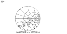
- FIG. 11 is a Smith chart showing impedance characteristics of the first filter when non-conduction and conduction of the first switch to the third switch are switched in the third embodiment.
- Embodiment 1 [1. Multiplexer Configuration] First, the configuration of the multiplexer according to the first embodiment will be described.
- FIG. 1 is a circuit configuration diagram of the multiplexer 1 according to the first embodiment.
- the antenna element ANT connected to the common terminal m1 of the multiplexer 1 is also illustrated in FIG.
- the antenna element ANT is a multi-band compatible antenna that transmits and receives high-frequency signals and that conforms to a communication standard such as LTE (Long Term Evolution), for example.
- LTE Long Term Evolution
- the multiplexer 1 includes a plurality of filters including the ladder-type first filter 10, and one input / output terminal (input / output terminals m11, m21 and m31) of each of the plurality of filters is commonly connected to the common terminal m1. It is a demultiplexing / multiplexing device.
- the plurality of filters have, for example, different pass bands.
- the multiplexer 1 is a triplexer comprising three filters. As shown in FIG. 1, the multiplexer 1 includes ladder-type first filters 10, second filters 20 and third filters 30.
- the other input / output terminals (input / output terminals m12, m22 and m23) of each of the plurality of filters are, for example, RF signal processing circuits via switch circuits or amplifier circuits such as power amplifiers and low noise amplifiers.
- RFIC Radio Frequency Integrated Circuit
- Which one of the first filter 10, the second filter 20, and the third filter 30 is used to perform communication is controlled by, for example, the RFIC.
- CA is performed by simultaneously using two or more of the first filter 10, the second filter 20, and the third filter 30.
- the first filter 10 is, for example, a high frequency filter having a pass band of Band 66 Rx (2110 to 2200 MHz) of LTE.
- the first filter 10 is, for example, a ladder-type elastic wave filter.
- the first filter 10 includes at least one series arm resonator connected on a path connecting one input / output terminal m11 (first input / output terminal) and the other input / output terminal m12 (second input / output terminal).
- the path may be a path connecting the common terminal m1 and the input / output terminal m12.
- the first filter 10 includes series arm resonators s11 to s14 connected in series with each other.
- the first filter 10 includes at least one parallel arm resonator connected between a connection node provided on the path and the ground.
- the connection node is a connection point between an element and an element or an element and a terminal, and is indicated by a point indicated by n1 or the like in FIG.
- the first filter 10 is a parallel arm resonator p11 connected between the node n1 between the series arm resonators s11 and s12 and the ground, and a series arm Parallel arm resonator p12 connected between node n2 between resonators s12 and s13 and ground, parallel arm resonator connected between node n3 between series arm resonators s13 and s14 and ground It has p13.
- the parallel arm resonator p11 is a first parallel arm resonator connected closest to the common terminal m1 among at least one parallel arm resonator (here, parallel arm resonators p11 to p13).
- the parallel arm resonator p11 is connected closest to the common terminal m1 among the at least one parallel arm resonators constituting the first filter 10, and therefore affects the impedance viewed from the common terminal m1 side of the first filter 10 It is easy to give a resonator.
- the connection closest to the common terminal m1 means that the connection is connected closest to the common terminal m1 in the circuit diagram. That is, for example, in the arrangement on the substrate or the like, the parallel arm resonator p11 may not be arranged closest to the common terminal m1 among the parallel arm resonators p11 to p13.
- At least one series arm resonator and at least one parallel arm resonator are resonators using elastic waves, for example, resonators using SAW (Surface Acoustic Wave), BAW (Bulk Acoustic Wave) It is a resonator or a film bulk acoustic resonator (FBAR).
- SAW Surface Acoustic Wave
- BAW Bulk Acoustic Wave
- FBAR film bulk acoustic resonator
- the SAW includes not only surface waves but also boundary waves.
- these resonators are SAW resonators.
- the high frequency filter can be configured by an IDT (Inter Digital Transducer) electrode formed on a substrate having piezoelectricity, so that a small and low-profile filter circuit having a high steepness pass characteristic can be realized.
- IDT Inter Digital Transducer
- the substrate having piezoelectricity is a substrate having piezoelectricity at least on the surface.
- the substrate may be provided with a piezoelectric thin film on the surface, and may be formed of a film having a speed of sound different from that of the piezoelectric thin film, and a laminated body such as a support substrate.
- the substrate is, for example, a laminate including a high sound velocity support substrate and a piezoelectric thin film formed on the high sound velocity support substrate, a high sound velocity support substrate, and a low sound velocity film formed on the high sound velocity support substrate.
- the first filter 10 further includes a switch SW1 (first switch).
- the switch SW1 is connected in series to the parallel arm resonator p11, and switches between conduction and non-conduction between the node n1 to which the parallel arm resonator p11 is connected and the ground.
- the non-conduction includes not only the non-conduction completely but also the case where a minute current such as a leak current flows.
- the switch SW1 is connected between the parallel arm resonator p11 and the ground, but may be connected between the node n1 and the parallel arm resonator p11.
- the switch SW1 is, for example, a SPST (Single Pole Single Throw) type switch element.
- the switch SW1 switches between conduction and non-conduction by a control signal from a control unit (not shown) such as RFIC, thereby making the connection node and the ground conductive or non-conductive.
- a control unit such as RFIC
- the switch SW1 may be a field effect transistor (FET) switch made of GaAs or complementary metal oxide semiconductor (CMOS), or a diode switch.
- FET field effect transistor
- CMOS complementary metal oxide semiconductor
- the switch SW1 Since the switch SW1 is not connected on the path connecting the common terminal m1 and the input / output terminal m12, the switch characteristic of the first filter 10 is unlikely to be affected. For example, when the switch is connected on the path, when using the first filter 10, the switch is made conductive. At this time, the pass characteristic and the reflection characteristic of the first filter 10 deteriorate due to the loss (on resistance) of the switch. Therefore, when the first filter 10 and another filter are used at the same time, the reflection characteristic of the first filter 10 is deteriorated, and the passage characteristic of the other filter is also deteriorated. Therefore, in the present invention, the switch is not connected on the path but connected in series with the parallel arm resonator.
- the parallel arm resonator p11 closest to the common terminal m1 is open.
- at least one series arm resonator is at least two series arm resonators, and parallel arm resonator p11 is connected closest to common terminal m1 among at least two series arm resonators. It is connected to the node n1 between the series arm resonator s11 (first series arm resonator) and the series arm resonator s12 (second series arm resonator) connected second most closely.
- the switch SW1 is in the non-conductive state, the combined capacitance of the two series arm resonators s11 and s12 connected in series decreases.
- the switch SW1 When the first filter 10 is used, for example, the switch SW1 is made conductive.
- the switch SW1 when any of the plurality of filters (the second filter 20 or the third filter 30) except the first filter 10 is used, the switch SW1 is rendered non-conductive. In this case, only the second filter 20 may be used, only the third filter 30 may be used, and both the second filter 20 and the third filter 30 may be used to perform CA. .
- the 2nd filter 20 or the 3rd filter 30 when the 1st filter 10 is also used (for example, at the time of 3CA where the 1st filter 10, the 2nd filter 20, and the 3rd filter 30 are used simultaneously) , The switch SW1 may be turned off.
- the number of series arm resonators provided in the first filter 10 is not limited to four, and the number of parallel arm resonators is not limited to three.
- the first filter 10 may include one to three or five or more series arm resonators, and may include one, two, or four or more parallel arm resonators.
- the first filter 10 may be configured to include only one series arm resonator s11, one parallel arm resonator p11, and the switch SW1.
- the second filter 20 is, for example, a filter having a Band 25 Rx (1930 to 1995 MHz) of LTE as a pass band.
- the second filter 20 is, for example, a ladder-type elastic wave filter.
- the second filter 20 includes series arm resonators s21 to s24 connected on a path connecting one input / output terminal m21 (common terminal m1) and the other input / output terminal m22.
- a parallel arm resonator p21 connected between the node between the series arm resonators s21 and s22 and the ground, a node between the series arm resonators s22 and s23 and the ground
- a parallel arm resonator p23 connected between a node between the series arm resonators s23 and s24 and the ground.
- the third filter 30 is, for example, a filter having a Band 30 Rx (2350 to 2360 MHz) of LTE as a pass band.
- the third filter 30 is, for example, a ladder-type elastic wave filter.
- the third filter 30 includes series arm resonators s31 to s34 connected on a path connecting one input / output terminal m31 (common terminal m1) and the other input / output terminal m32.
- the third filter 30 is connected between the node between the parallel arm resonator p31 connected between the node between the series arm resonators s31 and s32 and the ground, the node between the series arm resonators s32 and s33, and the ground.
- a parallel arm resonator p33 connected between a node between the series arm resonators s33 and s34 and the ground.
- FIG. 2A is a Smith chart showing impedance characteristics of the first filter 10 in the case where the switch SW1 is nonconductive (OFF) and conductive (ON) in the first embodiment.
- FIG. 2A is a Smith chart showing the impedance characteristics of the first filter 10 when viewed from the side of the input / output terminal m11 on the common terminal m1 side of the first filter 10.
- the second filter 20 and the third filter 30 are combined with the first filter 10 and It has been separated. That is, in FIG. 2A, the connection state of the first filter 10, the second filter 20, and the third filter 30 is not in the actual use state (the state shown in FIG.
- FIG. 2B is a graph showing the reflection loss of the first filter 10 in the case where the switch SW1 is nonconductive and in the case where the switch SW1 is conductive in the first embodiment.
- the second filter 20 and the third filter 30 are separated. It has become. That is, in FIG. 2B, the connection state of the first filter 10, the second filter 20, and the third filter 30 is not in the actual use state for the sake of explanation.
- the solid line indicates the reflection loss of the first filter 10 when the switch SW1 is nonconductive
- the broken line indicates the reflection loss of the first filter 10 when the switch SW1 is conductive.
- Each figure shows the filter characteristic of the first filter 10 outside the pass band (2110-2200 MHz) of the first filter 10 and in the pass band (1930-1995 MHz) of the second filter 20. The same applies to the drawings described below unless otherwise described.
- the switch SW1 is made nonconductive so that it is out of the passband of the first filter 10 (specifically, the second The impedance seen from the common terminal m1 side in the pass band of the filter 20: 1930 to 1995 MHz) is large.
- the parallel arm resonator p11 is connected closest to the common terminal m1 among the at least one parallel arm resonators constituting the first filter 10, and the impedance viewed from the common terminal m1 side of the first filter 10 It is because it is a resonator that easily affects the That is, by connecting the switch SW1 in series with the parallel arm resonator p11 and making the switch SW1 nonconductive to open the parallel arm resonator p11, the impedance can be increased.
- the series arm resonators s11 and s12 are connected close to the common terminal m1
- FIG. 3 is a graph showing the insertion loss of the second filter 20 in the case where the switch SW1 is nonconductive and in the case where the switch SW1 is conductive in the first embodiment.
- the connection state of the first filter 10, the second filter 20, and the third filter 30 is in the actual use state.
- the solid line indicates the insertion loss of the second filter 20 when the switch SW1 is nonconductive
- the broken line indicates the insertion loss of the second filter 20 when the switch SW1 is conductive.
- FIG. 3 shows the pass characteristic of the second filter 20 outside the pass band (2110-2200 MHz) of the first filter 10 and in the pass band (1930-1995 MHz) of the second filter 20.
- the switch SW1 when the switch SW1 is nonconductive, it is understood that the insertion loss in the pass band of the second filter 20 becomes smaller, and the pass characteristic of the second filter 20 is improved. Specifically, the insertion loss of the second filter 20 is 2.349 dB at 1930 MHz and 2.853 dB at 1995 MHz when the switch SW1 is on, whereas it is 1.52 at 1930 MHz when the switch SW1 is not on. It is improved to 28 dB and 2.552 dB at 1995 MHz.
- the parallel arm resonator p11 is a resonator that easily affects the impedance viewed from the common terminal m1 side of the first filter 10, and the parallel arm resonator p11 is parallel to open the parallel arm resonator p11.
- the switch SW1 is connected in series with the arm resonator p11.
- a comparative example in which the switch SW1 is not connected in series with the parallel arm resonator p11 will be described.
- FIG. 4 is a circuit configuration diagram of the first filter 100 according to the comparative example. Although not shown, the first filter 100, the second filter 20 and the third filter 30 constitute a multiplexer as shown in FIG.
- the switch SW1 is not connected to the parallel arm resonator p11, and the switch SW1a is connected to the parallel arm resonator p12.
- the parallel arm resonator p12 is not a resonator connected closest to the common terminal m1 among the at least one parallel arm resonators constituting the first filter 100, so the first filter 100 is more suitable than the parallel arm resonator p11.
- the resonator hardly affects the impedance viewed from the side of the common terminal m1.
- FIG. 5 is a graph showing the reflection loss of the first filters 10 and 100 when the first embodiment and the comparative example are compared.
- the second filter 20 and the third filter 30 are combined with the first filter 100. It has been separated. That is, in FIG. 5, the connection state of the first filter 100, the second filter 20, and the third filter 30 is not in the actual use state for the sake of explanation.
- the solid line indicates the reflection loss of the first filter 10 when the switch SW1 is nonconductive
- the broken line indicates the reflection loss of the first filter 10 when the switch SW1 is conductive
- the dashed dotted line indicates that the switch SW1a is nonconductive.
- the reflection loss of the 1st filter 100 in case of conduction is shown.
- the parallel arm resonator p12 is a resonator that is less likely to affect the impedance viewed from the common terminal m1 side of the first filter 100 than the parallel arm resonator p11. . Therefore, by connecting the switch SW1 in series with the parallel arm resonator p11 connected closest to the common terminal m1 among the at least one parallel arm resonators constituting the first filter 10 as in the present embodiment. The impedance viewed from the common terminal m1 side of the first filter 100 can be improved.
- the multiplexer 1 may include a matching circuit between the common terminal m1 and one of the input / output terminals m11, m21 and m31 of each filter.
- FIG. 6 is a circuit configuration diagram of the multiplexer 1 according to a modification of the first embodiment.
- the multiplexer 1 includes a matching circuit 11 for adjusting the impedance of the first filter 10 between the common terminal m1 and the input / output terminal m11, and the common terminal m1 and the input / output terminal m21
- a matching circuit 21 for adjusting the impedance of the second filter 20 is provided between them, and a matching circuit 31 for adjusting the impedance of the third filter 30 is provided between the common terminal m1 and the input / output terminal m31.
- the matching circuits 11, 21 and 31 are, for example, LC circuits or the like, but are not particularly limited.
- matching circuit 11, 21 and 31 do not include the switch.
- matching circuits 11, 21 and 31 are configured by shunt inductors.
- FIG. 7A is a Smith chart showing impedance characteristics of the first filter 10 in the case where the switch SW1 is nonconductive and in the case where the switch SW1 is conductive in the modification of the first embodiment.
- FIG. 7B is a graph showing the reflection loss of the first filter 10 when the switch SW1 is nonconductive and when it is conductive in the modification of the first embodiment.
- the second filter 20 and the third filter 30 are separated from the first filter 10.
- the impedance characteristics of the first filter 10 on the Smith chart in this modification are equal resistances in both the conduction and non-conduction of the switch SW1 compared to the impedance characteristics shown in FIG. 2A. It can be seen that the circle is rotated counterclockwise, and the impedance (particularly reactance) is increased. This is because a shunt inductor is connected between the common terminal m1 and the first filter 10 as the matching circuit 11.
- the reflection characteristics of the first filter 10 can be improved when the switch SW1 is nonconductive as compared to when the switch SW1 is conductive. .
- the matching circuit 11 may be connected between the common terminal m1 and the first filter 10 to increase the impedance viewed from the common terminal m1 outside the passband of the first filter 10.
- the switch SW1 is connected between the path connecting the common terminal m1 and the input / output terminal m12 and the ground, and is not connected on the path, so the first filter due to the loss of the switch Deterioration of the 10 filter characteristics can be suppressed.
- the parallel arm resonator p11 is closest to the common terminal m1 among the at least one parallel arm resonators constituting the first filter 10, and affects the impedance viewed from the common terminal m1 side of the first filter 10. It is an easy resonator. When the switch SW1 is in the non-conductive state, the parallel arm resonator p11 closest to the common terminal m1 is open.
- the impedance seen from the common terminal m1 side out of the pass band of the first filter 10 can be increased, and the reflection characteristic outside the pass band of the first filter 10 can be improved. That is, it is possible to configure the multiplexer 1 together with the first filter 10 and improve the pass characteristic of another filter (second filter 20 or the like) having the pass band outside the pass band.
- the present invention is particularly effective when a plurality of filters that can be used simultaneously in the multiplexer include a low priority filter and a high priority filter.
- the high priority filter is, for example, a filter corresponding to a frequently used frequency band, or a filter with a strict requirement specification.
- the filter of the first filter 10 since the parallel arm resonator p11 is opened when the switch SW1 is turned off in the first filter 10, the filter of the first filter 10 is not turned on when the switch SW1 is turned off. The characteristics deteriorate. Therefore, the first filter 10 may be used as a low priority filter.
- the second filter 20 may be used as a filter with higher priority than the first filter 10 because the filter characteristics are improved by the first filter 10.
- the two series arm resonators s11 and s12 are also connected close to the common terminal m1.
- the resonator easily affects the impedance viewed from the common terminal side of the first filter 10. Then, when the switch SW1 is in the non-conductive state, the parallel arm resonator p11 connected between the two series arm resonators s11 and s12 is open, so that the combined capacitance of the two series arm resonators s11 and s12 is It becomes smaller.
- the impedance viewed from the common terminal m1 side outside the pass band of the first filter 10 can be made larger, and the reflection characteristics outside the pass band of the first filter 10 can be further improved. That is, the pass characteristics of the other filters (the second filter 20 etc.) can be further improved.
- a plurality of filters constituting the multiplexer 1 may include a filter having a higher passband than the first filter 10.
- the first filter 10 has the lowest passband among the plurality of filters. It may be a filter.
- the resonance point of the parallel arm resonator p11 (a singular point at which the impedance of the resonator is minimized (ideally, the point at which the impedance is 0))
- the Q value of is degraded.
- the antiresonance point of the parallel arm resonator p11 (the singular point at which the impedance of the resonator reaches a maximum (ideally, the point at which the impedance is infinite)) forms the passband of the first filter 10 and the antiresonance
- the resonance point whose frequency is lower than that of the point forms an attenuation band lower than the pass band.
- the resonance point affects the attenuation characteristics of the attenuation band on the side lower than the pass band of the first filter 10, the Q value of the resonance point is deteriorated, so that the attenuation characteristic of the attenuation band is deteriorated.
- the pass band of the first filter 10 is as low as possible, for example, the lowest, and the attenuation band on the side lower than the pass band of the first filter 10 and other filters (for example, the third The pass band of the filter 30) can be made not to overlap, and the influence of the deterioration of the attenuation characteristic of the attenuation band on other filters can be suppressed.
- the at least one parallel arm resonator may include a parallel arm resonator whose resonance frequency is higher than the resonance frequency of the parallel arm resonator p11.
- the parallel arm resonator p11 is at least one.
- the parallel arm resonator having the lowest resonance frequency may be used.
- the Q value near the resonance point of the parallel arm resonator p11 is degraded by the loss (for example, the on resistance) of the switch SW1. Since the pass band of the filter is formed from the resonance point on the low band side of the parallel arm resonator to the antiresonance point on the high band side, the resonance frequency of the parallel arm resonator p11 whose Q value near the resonance point is degraded is As low as possible, for example, the lowest, it is possible to suppress the influence of the deterioration of the Q value on the pass characteristic of the first filter 10.
- the first filter 10a according to the second embodiment differs from the first filter 10 according to the first embodiment in that the series arm resonator s11 is not provided.
- the other points are the same as those of the first filter 10 according to the first embodiment, so the description will be omitted.
- the first filter 10 a constitutes a multiplexer together with the second filter 20 and the third filter 30.
- the pass band of the first filter 10a is the same Band 66 Rx (2110 to 2200 MHz) of LTE as the first filter 10.
- FIG. 8 is a circuit configuration diagram of the first filter 10a according to the second embodiment.
- the first filter 10a according to Embodiment 2 does not include the series arm resonator s11, and thus parallel arm resonance with the common terminal m1 (input / output terminal m11).
- the node n1 to which the child p11 is connected is connected without any one of at least one series arm resonator. Thereby, the node n1 becomes a connection node provided between the common terminal m1 (input / output terminal m11) and the series arm resonator s12.
- the series arm resonator is not connected to the common terminal m1 side of the node n1, in the first filter 10a, the parallel arm resonator p11 and the switch SW1 are connected in series as viewed from the common terminal m1 side. It is a ladder type filter that starts from the circuit.
- FIG. 9 is a Smith chart showing impedance characteristics of the first filter 10a in the case where the switch SW1 is nonconductive and in the case where the switch SW1 is conductive in the second embodiment. As in FIG. 2A, in FIG. 9, the second filter 20 and the third filter 30 are separated from the first filter 10a.
- the switch SW1 is made non-conductive, so that it is out of the passband of the first filter 10a (specifically, the second The impedance seen from the common terminal m1 side in the pass band of the filter 20: 1930 to 1995 MHz) is large.
- the impedance characteristic of the first filter 10a on the Smith chart in the present embodiment is at a position where the equal resistance circle is rotated clockwise as compared with the impedance characteristic of the first filter 10 shown in FIG. 2A. It can be seen that (especially the reactance) is reduced.
- the first filter 10a is a series arm resonator s11. It is because it is not equipped and the capacity
- the parallel arm resonator p11 when the switch SW1 is in the non-conductive state, the parallel arm resonator p11 is open, and the ladder type filter starts from the serial arm resonator s12 when the first filter 10a is viewed from the common terminal m1 side. It can be done.
- the first filter 10a when the switch SW1 is in the conductive state, the first filter 10a can be a ladder type filter starting from the parallel arm resonator p1.
- the impedance characteristic of the first filter 10a on the Smith chart in the present embodiment is compared with the impedance characteristic of the first filter 10 shown in FIG. 2A, when the switch SW1 is in the conductive state and in the non-conductive state.
- the impedance viewed from the common terminal m1 side of the first filter 10 is largely different between the ladder type filter starting from the series arm resonator s12 and the ladder type filter starting from the parallel arm resonator p11. Therefore, since the impedance viewed from the common terminal m1 side of the first filter 10a can be largely changed by the conduction / non-conduction of the switch SW1, the first filter 10a can also be used as an impedance adjustment circuit.
- the first filter 10b according to the third embodiment includes at least two parallel arm resonators, and among the at least two parallel arm resonators, switches are connected in series also to parallel arm resonators other than the parallel arm resonator p11. Is different from the first filter 10 according to the first embodiment.
- the first filter 10b according to the third embodiment is different from the first filter 10 according to the first embodiment in that the first filter 10b according to the third embodiment also includes the parallel arm resonator p14 and the series arm resonator s15. This shows that the number of series connections of arm resonators and the number of parallel connections of parallel arm resonators may be different from those in the first embodiment, and is not the main feature of the third embodiment, and therefore, the detailed description will be given. Omit.
- the first filter 10 b constitutes a multiplexer together with the second filter 20 and the third filter 30. Further, the pass band of the first filter 10 b is the same as Band 66 Rx (2110-2200 MHz) of LTE as the first filter 10.
- FIG. 10 is a circuit configuration diagram of the first filter 10b according to the third embodiment.
- the first filter 10b further includes a switch SW2 (second switch).
- the switch SW2 is connected in series to a parallel arm resonator p12 (second parallel arm resonator) connected to the other input / output terminal m12 side of the parallel arm resonator p11 among at least two parallel arm resonators. And switching between conduction and non-conduction between the node n2 to which the parallel arm resonator p12 is connected and the ground.
- at least one series arm resonator (here, a series arm resonator) between the node n1 to which the parallel arm resonator p11 is connected and the node n2 to which the parallel arm resonator p12 is connected. s12) is connected.
- the parallel arm resonator p12 is connected second closest to the common terminal m1 (input / output terminal m11) among the at least two parallel arm resonators.
- the first filter 10b may not include the series arm resonator s12, and none of at least one series arm resonator may be connected between the node n1 and the node n2.
- the first filter 10b includes a switch SW3 (third switch).
- the switch SW3 is connected in series with the parallel arm resonator p13 connected to the other input / output terminal m12 side of the parallel arm resonator p11 among the at least two parallel arm resonators, and the parallel arm resonator p13 is connected Switching between conduction and non-conduction between the node n3 and the ground.
- at least one series arm resonator (here, a series arm resonator) between the node n2 to which the parallel arm resonator p12 is connected and the node n3 to which the parallel arm resonator p13 is connected. s13) is connected. As shown in FIG.
- the parallel arm resonator p13 is connected third closest to the common terminal m1 (input / output terminal m11) among the at least two parallel arm resonators.
- the first filter 10b may not include the series arm resonator s13, and none of at least one series arm resonator may be connected between the node n2 and the node n3.
- the parallel arm resonator connected closer to the input / output terminal m12 than the parallel arm resonator p11 is also used.
- the switches are connected in series.
- the first filter 10b may not have any of the switches SW2 and SW3, and may be connected in series with the parallel arm resonator p14.
- FIG. 11 is a Smith chart showing the impedance characteristic of the first filter 10b when the non-conduction and conduction of the switch SW3 are switched from the switch SW1 in the third embodiment.
- the second filter 20 and the third filter 30 are separated from the first filter 10b.
- “All SW ON” shown in FIG. 11 indicates the impedance characteristic of the first filter 10b when all the switches SW1 to SW3 are in the conductive state.
- “SW1 OFF” indicates the impedance characteristic of the first filter 10b when only the switch SW1 is in the non-conductive state and the switches SW2 and SW3 are in the conductive state.
- SW1, SW2 OFF indicates the impedance characteristic of the first filter 10b when the switches SW1 and SW2 are turned off and only the switch SW3 is turned on.
- All SW OFF indicates the impedance characteristic of the first filter 10b when all the switches SW1 to SW3 are in the non-conductive state.
- the switch is also connected to the parallel arm resonators other than the parallel arm resonator p11 connected closest to the common terminal m1.
- the impedance viewed from the common terminal m1 side can be flexibly adjusted.
- the parallel arm resonator p12 is the second closest to the common terminal m1 among the at least one parallel arm resonators constituting the first filter 10b, and affects the impedance viewed from the common terminal m1 side of the first filter 10b.
- the impedance can be adjusted more flexibly by connecting the switch SW2 to the parallel arm resonator p12 as a parallel arm resonator other than the parallel arm resonator p11.
- the multiplexer 1 is a triplexer, but may be a duplexer, a quadplexer, or the like.
- the pass band of the first filters 10, 10a and 10b is Band 66 Rx (2110-2200 MHz) of LTE
- the pass band of the second filter 20 is Band 25 Rx (1930-1995 MHz) of LTE
- the pass band of the third filter 30 is the Band 30 Rx (2350-2360 MHz) of LTE, but these are an example, and are appropriately determined according to the required specifications.
- the second filter 20 and the third filter 30 are ladder-type elastic wave filters, but may be LC filters or the like.
- the switch SW1 is connected in series with the parallel arm resonator p11 connected closest to the common terminal m1, but is connected in series with any one of at least one parallel arm resonator It should just be. That is, the switch SW1 may not necessarily be connected in series with the parallel arm resonator p11 connected closest to the common terminal m1.
- the present invention can be widely used in communication devices such as mobile phones as multiplexers and high frequency filters applicable to multi-band systems.
Landscapes
- Physics & Mathematics (AREA)
- Acoustics & Sound (AREA)
- Chemical & Material Sciences (AREA)
- Crystallography & Structural Chemistry (AREA)
- Surface Acoustic Wave Elements And Circuit Networks Thereof (AREA)
- Piezo-Electric Or Mechanical Vibrators, Or Delay Or Filter Circuits (AREA)
Abstract
Priority Applications (4)
| Application Number | Priority Date | Filing Date | Title |
|---|---|---|---|
| CN201880064910.2A CN111183585B (zh) | 2017-10-10 | 2018-10-04 | 多工器 |
| KR1020207007756A KR102368022B1 (ko) | 2017-10-10 | 2018-10-04 | 멀티플렉서 및 고주파 필터 |
| JP2019548162A JP6822580B2 (ja) | 2017-10-10 | 2018-10-04 | マルチプレクサおよび高周波フィルタ |
| US16/830,318 US11881841B2 (en) | 2017-10-10 | 2020-03-26 | Multiplexer and high-frequency filter |
Applications Claiming Priority (2)
| Application Number | Priority Date | Filing Date | Title |
|---|---|---|---|
| JP2017197048 | 2017-10-10 | ||
| JP2017-197048 | 2017-10-10 |
Related Child Applications (1)
| Application Number | Title | Priority Date | Filing Date |
|---|---|---|---|
| US16/830,318 Continuation US11881841B2 (en) | 2017-10-10 | 2020-03-26 | Multiplexer and high-frequency filter |
Publications (1)
| Publication Number | Publication Date |
|---|---|
| WO2019073899A1 true WO2019073899A1 (fr) | 2019-04-18 |
Family
ID=66100853
Family Applications (1)
| Application Number | Title | Priority Date | Filing Date |
|---|---|---|---|
| PCT/JP2018/037225 Ceased WO2019073899A1 (fr) | 2017-10-10 | 2018-10-04 | Multiplexeur et filtre haute fréquence |
Country Status (5)
| Country | Link |
|---|---|
| US (1) | US11881841B2 (fr) |
| JP (1) | JP6822580B2 (fr) |
| KR (1) | KR102368022B1 (fr) |
| CN (1) | CN111183585B (fr) |
| WO (1) | WO2019073899A1 (fr) |
Cited By (1)
| Publication number | Priority date | Publication date | Assignee | Title |
|---|---|---|---|---|
| JP2021027382A (ja) * | 2019-07-31 | 2021-02-22 | 太陽誘電株式会社 | 弾性波デバイスおよびその製造方法、圧電薄膜共振器、フィルタ並びにマルチプレクサ |
Families Citing this family (5)
| Publication number | Priority date | Publication date | Assignee | Title |
|---|---|---|---|---|
| WO2019073899A1 (fr) * | 2017-10-10 | 2019-04-18 | 株式会社村田製作所 | Multiplexeur et filtre haute fréquence |
| US20220029646A1 (en) * | 2020-07-27 | 2022-01-27 | Corning Research & Development Corporation | Radio frequency transceiver filter circuit having inter-stage impedance matching |
| CN112511131B (zh) * | 2021-02-05 | 2021-05-25 | 成都频岢微电子有限公司 | 一种具有高隔离度和高通频带低频侧高陡峭度的双工器 |
| JP7853021B2 (ja) * | 2021-05-28 | 2026-04-28 | スカイワークス ソリューションズ,インコーポレイテッド | スイッチング可能弾性波フィルタを備えるマルチプレクサ、無線通信デバイス、及びスイッチング可能フィルタ |
| US12542568B2 (en) * | 2021-11-08 | 2026-02-03 | Skyworks Solutions, Inc. | Power rugged filter module |
Citations (7)
| Publication number | Priority date | Publication date | Assignee | Title |
|---|---|---|---|---|
| US20090251235A1 (en) * | 2008-02-15 | 2009-10-08 | Stmicroelectronics S.A. | Bulk acoustic wave resonator filter being digitally reconfigurable, with process |
| JP2010252254A (ja) * | 2009-04-20 | 2010-11-04 | Murata Mfg Co Ltd | 弾性波フィルタ及び分波器 |
| US20110299432A1 (en) * | 2009-12-03 | 2011-12-08 | Rf Micro Devices, Inc. | Sub-band duplexer with active frequency tuning |
| WO2014167755A1 (fr) * | 2013-04-08 | 2014-10-16 | 株式会社村田製作所 | Duplexeur |
| WO2015099105A1 (fr) * | 2013-12-27 | 2015-07-02 | 株式会社村田製作所 | Filtre à haute fréquence |
| WO2016026607A1 (fr) * | 2014-08-20 | 2016-02-25 | Epcos Ag | Filtre hf accordable comprenant des résonateurs en parallèle |
| WO2017138540A1 (fr) * | 2016-02-08 | 2017-08-17 | 株式会社村田製作所 | Circuit de filtrage haute fréquence, duplexeur, circuit frontal haute fréquence, et dispositif de communication |
Family Cites Families (46)
| Publication number | Priority date | Publication date | Assignee | Title |
|---|---|---|---|---|
| JP3878714B2 (ja) * | 1997-04-24 | 2007-02-07 | 京セラ株式会社 | 弾性表面波フィルタ |
| JP4943137B2 (ja) | 2006-12-25 | 2012-05-30 | 京セラ株式会社 | 分波器および通信装置 |
| JP5441095B2 (ja) * | 2008-01-31 | 2014-03-12 | 太陽誘電株式会社 | 弾性波デバイス、デュープレクサ、通信モジュール、および通信装置 |
| US9246536B2 (en) * | 2009-12-03 | 2016-01-26 | Rf Micro Devices, Inc. | Duplexer with active temperature compensation |
| JP5859579B2 (ja) * | 2012-02-06 | 2016-02-10 | 太陽誘電株式会社 | フィルタ回路およびモジュール |
| US9654169B2 (en) | 2014-04-22 | 2017-05-16 | Skyworks Solutions, Inc. | Apparatus and methods for multi-band radio frequency signal routing |
| WO2017138539A1 (fr) * | 2016-02-08 | 2017-08-17 | 株式会社村田製作所 | Circuit frontal à haute fréquence et dispositif de communication |
| JP6411398B2 (ja) * | 2016-03-14 | 2018-10-24 | 太陽誘電株式会社 | フィルタ回路、フロントエンド回路およびモジュール |
| WO2017170071A1 (fr) * | 2016-03-31 | 2017-10-05 | 株式会社村田製作所 | Filtre à fréquence variable, circuit rf frontal et terminal de communication |
| WO2017199649A1 (fr) * | 2016-05-20 | 2017-11-23 | 株式会社村田製作所 | Circuit frontal à haute fréquence et dispositif de communication |
| CN109196778B (zh) * | 2016-05-27 | 2022-06-14 | 株式会社村田制作所 | 高频滤波电路、高频前端电路以及通信装置 |
| WO2017204347A1 (fr) * | 2016-05-27 | 2017-11-30 | 株式会社村田製作所 | Dispositif de filtre haute fréquence et dispositif de communication |
| KR102115112B1 (ko) * | 2016-05-27 | 2020-05-25 | 가부시키가이샤 무라타 세이사쿠쇼 | 고주파 필터 회로, 멀티플렉서, 고주파 프론트 엔드 회로 및 통신 장치 |
| CN109478882B (zh) * | 2016-07-15 | 2022-08-23 | 株式会社村田制作所 | 多工器、高频前端电路以及通信终端 |
| WO2018037967A1 (fr) * | 2016-08-23 | 2018-03-01 | 株式会社村田製作所 | Dispositif de filtrage, circuit frontal à haute fréquence, et dispositif de communication |
| WO2018037968A1 (fr) * | 2016-08-26 | 2018-03-01 | 株式会社村田製作所 | Dispositif de filtre à onde élastique, multiplexeur, circuit frontal haute fréquence et dispositif de communication |
| WO2018043607A1 (fr) * | 2016-09-02 | 2018-03-08 | 株式会社村田製作所 | Dispositif de filtre à ondes acoustiques, circuit frontal à haute fréquence, et dispositif de communication |
| WO2018043606A1 (fr) * | 2016-09-02 | 2018-03-08 | 株式会社村田製作所 | Dispositif de filtre à ondes élastiques, circuit frontal à haute fréquence, et appareil de communication |
| WO2018043608A1 (fr) * | 2016-09-02 | 2018-03-08 | 株式会社村田製作所 | Dispositif de filtre d'onde acoustique, circuit frontal à haute fréquence, et appareil de communication |
| WO2018051864A1 (fr) * | 2016-09-16 | 2018-03-22 | 株式会社村田製作所 | Circuit frontal haute fréquence et appareil de communication |
| WO2018056224A1 (fr) * | 2016-09-21 | 2018-03-29 | 株式会社村田製作所 | Dispositif à ondes élastiques, circuit frontal à haute fréquence et dispositif de communication |
| CN109792238B (zh) * | 2016-09-26 | 2023-01-03 | 株式会社村田制作所 | 弹性波滤波器装置、高频前端电路以及通信装置 |
| WO2018061878A1 (fr) * | 2016-09-29 | 2018-04-05 | 株式会社村田製作所 | Dispositif d'ondes élastiques, circuit frontal haute fréquence, et dispositif de communication |
| WO2018061949A1 (fr) * | 2016-09-29 | 2018-04-05 | 株式会社村田製作所 | Dispositif de filtre à ondes acoustiques, multiplexeur, circuit frontal à haute fréquence et dispositif de communication |
| WO2018061950A1 (fr) * | 2016-09-29 | 2018-04-05 | 株式会社村田製作所 | Dispositif de filtre à ondes acoustiques, multiplexeur, circuit frontal haute fréquence et dispositif de communication |
| WO2018135538A1 (fr) * | 2017-01-19 | 2018-07-26 | 株式会社村田製作所 | Filtre haute fréquence, circuit frontal haute fréquence et dispositif de communication |
| US10547286B2 (en) * | 2017-02-03 | 2020-01-28 | Samsung Electro-Mechanics Co., Ltd. | Filter and front end module including the same |
| WO2018147135A1 (fr) * | 2017-02-07 | 2018-08-16 | 株式会社村田製作所 | Filtre haute fréquence, circuit frontal haute fréquence et dispositif de communication |
| WO2018151218A1 (fr) * | 2017-02-20 | 2018-08-23 | 株式会社村田製作所 | Dispositif filtre, multiplexeur, circuit frontal haute fréquence et dispositif de communication |
| CN110383687B (zh) * | 2017-03-01 | 2023-02-17 | 株式会社村田制作所 | 高频滤波器、多工器、高频前端电路以及通信装置 |
| WO2018168655A1 (fr) * | 2017-03-15 | 2018-09-20 | 株式会社村田製作所 | Multiplexeur, circuit frontal haute fréquence, et dispositif de communication |
| WO2018186227A1 (fr) * | 2017-04-03 | 2018-10-11 | 株式会社村田製作所 | Dispositif de filtre à ondes élastiques, multiplexeur, circuit frontal haute fréquence et dispositif de communication |
| CN110663179B (zh) * | 2017-05-18 | 2023-03-21 | 株式会社村田制作所 | 多工器、高频电路以及通信装置 |
| WO2019003619A1 (fr) * | 2017-06-28 | 2019-01-03 | 株式会社村田製作所 | Filtre haute fréquence, multiplexeur, circuit frontal haute fréquence et dispositif de communication |
| WO2019003855A1 (fr) * | 2017-06-28 | 2019-01-03 | 株式会社村田製作所 | Filtre haute fréquence, multiplexeur, circuit frontal haute fréquence et dispositif de communication |
| WO2019012822A1 (fr) * | 2017-07-10 | 2019-01-17 | 株式会社村田製作所 | Filtre haute fréquence, multiplexeur, circuit frontal haute fréquence et dispositif de communication |
| WO2019013015A1 (fr) * | 2017-07-10 | 2019-01-17 | 株式会社村田製作所 | Filtre haute fréquence, multiplexeur, circuit frontal haute fréquence et dispositif de communication |
| CN111034042B (zh) * | 2017-08-28 | 2023-06-02 | 株式会社村田制作所 | 滤波器装置、多工器、高频前端电路以及通信装置 |
| WO2019073899A1 (fr) * | 2017-10-10 | 2019-04-18 | 株式会社村田製作所 | Multiplexeur et filtre haute fréquence |
| WO2019078157A1 (fr) * | 2017-10-16 | 2019-04-25 | 株式会社村田製作所 | Filtre à ondes acoustiques, multiplexeur, circuit frontal haute fréquence et dispositif de communication |
| WO2019188864A1 (fr) * | 2018-03-28 | 2019-10-03 | 株式会社村田製作所 | Filtre à ondes élastiques, multiplexeur, circuit frontal haute fréquence et dispositif de communication |
| US10659086B2 (en) * | 2018-06-13 | 2020-05-19 | Qorvo Us, Inc. | Multi-mode radio frequency circuit |
| WO2020059352A1 (fr) * | 2018-09-19 | 2020-03-26 | 株式会社村田製作所 | Dispositif de filtre, circuit frontal haute fréquence et dispositif de communication utilisant ledit dispositif de filtre |
| US11563421B2 (en) * | 2018-09-21 | 2023-01-24 | Qorvo Us, Inc. | Acoustic structure having tunable parallel resonance frequency |
| JP2021064874A (ja) * | 2019-10-15 | 2021-04-22 | 株式会社村田製作所 | 高周波モジュールおよび通信装置 |
| JP7853021B2 (ja) * | 2021-05-28 | 2026-04-28 | スカイワークス ソリューションズ,インコーポレイテッド | スイッチング可能弾性波フィルタを備えるマルチプレクサ、無線通信デバイス、及びスイッチング可能フィルタ |
-
2018
- 2018-10-04 WO PCT/JP2018/037225 patent/WO2019073899A1/fr not_active Ceased
- 2018-10-04 KR KR1020207007756A patent/KR102368022B1/ko active Active
- 2018-10-04 JP JP2019548162A patent/JP6822580B2/ja active Active
- 2018-10-04 CN CN201880064910.2A patent/CN111183585B/zh active Active
-
2020
- 2020-03-26 US US16/830,318 patent/US11881841B2/en active Active
Patent Citations (7)
| Publication number | Priority date | Publication date | Assignee | Title |
|---|---|---|---|---|
| US20090251235A1 (en) * | 2008-02-15 | 2009-10-08 | Stmicroelectronics S.A. | Bulk acoustic wave resonator filter being digitally reconfigurable, with process |
| JP2010252254A (ja) * | 2009-04-20 | 2010-11-04 | Murata Mfg Co Ltd | 弾性波フィルタ及び分波器 |
| US20110299432A1 (en) * | 2009-12-03 | 2011-12-08 | Rf Micro Devices, Inc. | Sub-band duplexer with active frequency tuning |
| WO2014167755A1 (fr) * | 2013-04-08 | 2014-10-16 | 株式会社村田製作所 | Duplexeur |
| WO2015099105A1 (fr) * | 2013-12-27 | 2015-07-02 | 株式会社村田製作所 | Filtre à haute fréquence |
| WO2016026607A1 (fr) * | 2014-08-20 | 2016-02-25 | Epcos Ag | Filtre hf accordable comprenant des résonateurs en parallèle |
| WO2017138540A1 (fr) * | 2016-02-08 | 2017-08-17 | 株式会社村田製作所 | Circuit de filtrage haute fréquence, duplexeur, circuit frontal haute fréquence, et dispositif de communication |
Cited By (2)
| Publication number | Priority date | Publication date | Assignee | Title |
|---|---|---|---|---|
| JP2021027382A (ja) * | 2019-07-31 | 2021-02-22 | 太陽誘電株式会社 | 弾性波デバイスおよびその製造方法、圧電薄膜共振器、フィルタ並びにマルチプレクサ |
| JP7383417B2 (ja) | 2019-07-31 | 2023-11-20 | 太陽誘電株式会社 | 弾性波デバイスおよびその製造方法、圧電薄膜共振器、フィルタ並びにマルチプレクサ |
Also Published As
| Publication number | Publication date |
|---|---|
| KR20200039774A (ko) | 2020-04-16 |
| CN111183585A (zh) | 2020-05-19 |
| CN111183585B (zh) | 2023-09-15 |
| KR102368022B1 (ko) | 2022-02-25 |
| JPWO2019073899A1 (ja) | 2020-09-03 |
| US11881841B2 (en) | 2024-01-23 |
| US20200228097A1 (en) | 2020-07-16 |
| JP6822580B2 (ja) | 2021-01-27 |
Similar Documents
| Publication | Publication Date | Title |
|---|---|---|
| CN108023568B (zh) | 滤波器装置、多路复用器、高频前置电路以及通信装置 | |
| JP6822580B2 (ja) | マルチプレクサおよび高周波フィルタ | |
| CN109286387B (zh) | 高频滤波器、多路复用器、高频前置电路以及通信装置 | |
| KR101986022B1 (ko) | 멀티플렉서 | |
| JP6516018B2 (ja) | スイッチモジュール | |
| US10333484B2 (en) | Filter modules and filter arrays having inductive impedance | |
| US10547288B2 (en) | Radio frequency front-end circuit and communication device | |
| CN107733448B (zh) | 开关电路、高频模块以及通信装置 | |
| JP6687161B2 (ja) | スイッチモジュール | |
| WO2017204346A1 (fr) | Circuit de filtrage haute fréquence, multiplexeur, circuit frontal haute fréquence et dispositif de communication | |
| WO2019064990A1 (fr) | Filtre haute fréquence, multiplexeur, circuit frontal haute fréquence et dispositif de communication | |
| JP6798456B2 (ja) | 高周波フロントエンド回路及び通信装置 | |
| WO2020008759A1 (fr) | Filtre haute fréquence, multiplexeur, circuit frontal haute fréquence et dispositif de communication | |
| JP2018078542A (ja) | フィルタ装置、マルチプレクサ、高周波フロントエンド回路及び通信装置 | |
| WO2018061950A1 (fr) | Dispositif de filtre à ondes acoustiques, multiplexeur, circuit frontal haute fréquence et dispositif de communication | |
| WO2018168655A1 (fr) | Multiplexeur, circuit frontal haute fréquence, et dispositif de communication | |
| WO2018061949A1 (fr) | Dispositif de filtre à ondes acoustiques, multiplexeur, circuit frontal à haute fréquence et dispositif de communication | |
| JP2018026795A (ja) | 高周波モジュール及び通信装置 | |
| CN109792238B (zh) | 弹性波滤波器装置、高频前端电路以及通信装置 | |
| WO2019044034A1 (fr) | Module haute fréquence, module frontal et dispositif de communication | |
| WO2018061783A1 (fr) | Dispositif de filtre d'onde élastique, circuit frontal haute fréquence et dispositif de communication | |
| JP2019096971A (ja) | 高周波フィルタおよびマルチプレクサ | |
| JPWO2019131868A1 (ja) | フィルタモジュール |
Legal Events
| Date | Code | Title | Description |
|---|---|---|---|
| 121 | Ep: the epo has been informed by wipo that ep was designated in this application |
Ref document number: 18866559 Country of ref document: EP Kind code of ref document: A1 |
|
| ENP | Entry into the national phase |
Ref document number: 2019548162 Country of ref document: JP Kind code of ref document: A |
|
| ENP | Entry into the national phase |
Ref document number: 20207007756 Country of ref document: KR Kind code of ref document: A |
|
| NENP | Non-entry into the national phase |
Ref country code: DE |
|
| 122 | Ep: pct application non-entry in european phase |
Ref document number: 18866559 Country of ref document: EP Kind code of ref document: A1 |