WO2017203828A1 - Système d'alimentation électrique - Google Patents
Système d'alimentation électrique Download PDFInfo
- Publication number
- WO2017203828A1 WO2017203828A1 PCT/JP2017/012935 JP2017012935W WO2017203828A1 WO 2017203828 A1 WO2017203828 A1 WO 2017203828A1 JP 2017012935 W JP2017012935 W JP 2017012935W WO 2017203828 A1 WO2017203828 A1 WO 2017203828A1
- Authority
- WO
- WIPO (PCT)
- Prior art keywords
- switch
- terminal
- capacitor
- current
- inductive load
- Prior art date
- Legal status (The legal status is an assumption and is not a legal conclusion. Google has not performed a legal analysis and makes no representation as to the accuracy of the status listed.)
- Ceased
Links
Images




Classifications
-
- H—ELECTRICITY
- H02—GENERATION; CONVERSION OR DISTRIBUTION OF ELECTRIC POWER
- H02M—APPARATUS FOR CONVERSION BETWEEN AC AND AC, BETWEEN AC AND DC, OR BETWEEN DC AND DC, AND FOR USE WITH MAINS OR SIMILAR POWER SUPPLY SYSTEMS; CONVERSION OF DC OR AC INPUT POWER INTO SURGE OUTPUT POWER; CONTROL OR REGULATION THEREOF
- H02M7/00—Conversion of AC power input into DC power output; Conversion of DC power input into AC power output
- H02M7/42—Conversion of DC power input into AC power output without possibility of reversal
- H02M7/44—Conversion of DC power input into AC power output without possibility of reversal by static converters
- H02M7/48—Conversion of DC power input into AC power output without possibility of reversal by static converters using discharge tubes with control electrode or semiconductor devices with control electrode
- H02M7/53—Conversion of DC power input into AC power output without possibility of reversal by static converters using discharge tubes with control electrode or semiconductor devices with control electrode using devices of a triode or transistor type requiring continuous application of a control signal
- H02M7/537—Conversion of DC power input into AC power output without possibility of reversal by static converters using discharge tubes with control electrode or semiconductor devices with control electrode using devices of a triode or transistor type requiring continuous application of a control signal using semiconductor devices only, e.g. single switched pulse inverters
- H02M7/5387—Conversion of DC power input into AC power output without possibility of reversal by static converters using discharge tubes with control electrode or semiconductor devices with control electrode using devices of a triode or transistor type requiring continuous application of a control signal using semiconductor devices only, e.g. single switched pulse inverters in a bridge configuration
- H02M7/53871—Conversion of DC power input into AC power output without possibility of reversal by static converters using discharge tubes with control electrode or semiconductor devices with control electrode using devices of a triode or transistor type requiring continuous application of a control signal using semiconductor devices only, e.g. single switched pulse inverters in a bridge configuration with automatic control of output voltage or current
-
- H—ELECTRICITY
- H02—GENERATION; CONVERSION OR DISTRIBUTION OF ELECTRIC POWER
- H02M—APPARATUS FOR CONVERSION BETWEEN AC AND AC, BETWEEN AC AND DC, OR BETWEEN DC AND DC, AND FOR USE WITH MAINS OR SIMILAR POWER SUPPLY SYSTEMS; CONVERSION OF DC OR AC INPUT POWER INTO SURGE OUTPUT POWER; CONTROL OR REGULATION THEREOF
- H02M7/00—Conversion of AC power input into DC power output; Conversion of DC power input into AC power output
- H02M7/42—Conversion of DC power input into AC power output without possibility of reversal
- H02M7/44—Conversion of DC power input into AC power output without possibility of reversal by static converters
- H02M7/48—Conversion of DC power input into AC power output without possibility of reversal by static converters using discharge tubes with control electrode or semiconductor devices with control electrode
- H02M7/4826—Conversion of DC power input into AC power output without possibility of reversal by static converters using discharge tubes with control electrode or semiconductor devices with control electrode operating from a resonant DC source, i.e. the DC input voltage varies periodically, e.g. resonant DC-link inverters
-
- H—ELECTRICITY
- H02—GENERATION; CONVERSION OR DISTRIBUTION OF ELECTRIC POWER
- H02J—ELECTRIC POWER NETWORKS; CIRCUIT ARRANGEMENTS OR SYSTEMS FOR SUPPLYING OR DISTRIBUTING ELECTRIC POWER; SYSTEMS FOR STORING ELECTRIC ENERGY
- H02J7/00—Circuit arrangements for charging or discharging batteries or for supplying loads from batteries
- H02J7/34—Parallel operation in networks using both storage and other DC sources, e.g. providing buffering
- H02J7/345—Parallel operation in networks using both storage and other DC sources, e.g. providing buffering using capacitors as storage or buffering devices
-
- H—ELECTRICITY
- H02—GENERATION; CONVERSION OR DISTRIBUTION OF ELECTRIC POWER
- H02M—APPARATUS FOR CONVERSION BETWEEN AC AND AC, BETWEEN AC AND DC, OR BETWEEN DC AND DC, AND FOR USE WITH MAINS OR SIMILAR POWER SUPPLY SYSTEMS; CONVERSION OF DC OR AC INPUT POWER INTO SURGE OUTPUT POWER; CONTROL OR REGULATION THEREOF
- H02M1/00—Details of apparatus for conversion
- H02M1/08—Circuits specially adapted for the generation of control voltages for semiconductor devices incorporated in static converters
-
- H—ELECTRICITY
- H02—GENERATION; CONVERSION OR DISTRIBUTION OF ELECTRIC POWER
- H02M—APPARATUS FOR CONVERSION BETWEEN AC AND AC, BETWEEN AC AND DC, OR BETWEEN DC AND DC, AND FOR USE WITH MAINS OR SIMILAR POWER SUPPLY SYSTEMS; CONVERSION OF DC OR AC INPUT POWER INTO SURGE OUTPUT POWER; CONTROL OR REGULATION THEREOF
- H02M11/00—Power conversion systems not covered by the preceding groups
-
- H—ELECTRICITY
- H02—GENERATION; CONVERSION OR DISTRIBUTION OF ELECTRIC POWER
- H02M—APPARATUS FOR CONVERSION BETWEEN AC AND AC, BETWEEN AC AND DC, OR BETWEEN DC AND DC, AND FOR USE WITH MAINS OR SIMILAR POWER SUPPLY SYSTEMS; CONVERSION OF DC OR AC INPUT POWER INTO SURGE OUTPUT POWER; CONTROL OR REGULATION THEREOF
- H02M7/00—Conversion of AC power input into DC power output; Conversion of DC power input into AC power output
- H02M7/42—Conversion of DC power input into AC power output without possibility of reversal
- H02M7/44—Conversion of DC power input into AC power output without possibility of reversal by static converters
- H02M7/48—Conversion of DC power input into AC power output without possibility of reversal by static converters using discharge tubes with control electrode or semiconductor devices with control electrode
- H02M7/4815—Resonant converters
- H02M7/4818—Resonant converters with means for adaptation of resonance frequency, e.g. by modification of capacitance or inductance of resonance circuits
-
- H—ELECTRICITY
- H05—ELECTRIC TECHNIQUES NOT OTHERWISE PROVIDED FOR
- H05B—ELECTRIC HEATING; ELECTRIC LIGHT SOURCES NOT OTHERWISE PROVIDED FOR; CIRCUIT ARRANGEMENTS FOR ELECTRIC LIGHT SOURCES, IN GENERAL
- H05B6/00—Heating by electric, magnetic or electromagnetic fields
- H05B6/02—Induction heating
- H05B6/04—Sources of current
-
- H—ELECTRICITY
- H05—ELECTRIC TECHNIQUES NOT OTHERWISE PROVIDED FOR
- H05B—ELECTRIC HEATING; ELECTRIC LIGHT SOURCES NOT OTHERWISE PROVIDED FOR; CIRCUIT ARRANGEMENTS FOR ELECTRIC LIGHT SOURCES, IN GENERAL
- H05B6/00—Heating by electric, magnetic or electromagnetic fields
- H05B6/02—Induction heating
- H05B6/06—Control, e.g. of temperature, of power
-
- H—ELECTRICITY
- H02—GENERATION; CONVERSION OR DISTRIBUTION OF ELECTRIC POWER
- H02M—APPARATUS FOR CONVERSION BETWEEN AC AND AC, BETWEEN AC AND DC, OR BETWEEN DC AND DC, AND FOR USE WITH MAINS OR SIMILAR POWER SUPPLY SYSTEMS; CONVERSION OF DC OR AC INPUT POWER INTO SURGE OUTPUT POWER; CONTROL OR REGULATION THEREOF
- H02M7/00—Conversion of AC power input into DC power output; Conversion of DC power input into AC power output
- H02M7/42—Conversion of DC power input into AC power output without possibility of reversal
- H02M7/44—Conversion of DC power input into AC power output without possibility of reversal by static converters
- H02M7/48—Conversion of DC power input into AC power output without possibility of reversal by static converters using discharge tubes with control electrode or semiconductor devices with control electrode
- H02M7/4815—Resonant converters
-
- Y—GENERAL TAGGING OF NEW TECHNOLOGICAL DEVELOPMENTS; GENERAL TAGGING OF CROSS-SECTIONAL TECHNOLOGIES SPANNING OVER SEVERAL SECTIONS OF THE IPC; TECHNICAL SUBJECTS COVERED BY FORMER USPC CROSS-REFERENCE ART COLLECTIONS [XRACs] AND DIGESTS
- Y02—TECHNOLOGIES OR APPLICATIONS FOR MITIGATION OR ADAPTATION AGAINST CLIMATE CHANGE
- Y02B—CLIMATE CHANGE MITIGATION TECHNOLOGIES RELATED TO BUILDINGS, e.g. HOUSING, HOUSE APPLIANCES OR RELATED END-USER APPLICATIONS
- Y02B70/00—Technologies for an efficient end-user side electric power management and consumption
- Y02B70/10—Technologies improving the efficiency by using switched-mode power supplies [SMPS], i.e. efficient power electronics conversion e.g. power factor correction or reduction of losses in power supplies or efficient standby modes
Definitions
- the present invention relates to a power supply system, and is particularly suitable for use in converting DC power to AC power.
- the magnetic energy regenerative switch described in Patent Document 1 has four switches and a capacitor.
- the four switches are connected to form a full bridge circuit.
- the capacitor is connected between the DC terminals of the full bridge circuit.
- the load is connected between the output terminals of the full bridge circuit.
- the four switches have a positive terminal and a negative terminal.
- the conduction state from the negative terminal to the positive terminal of the four switches is a state in which current always flows.
- the conduction state from the positive terminal to the negative terminal of the four switches is switched between a state in which current flows and a state in which no current flows by an external signal.
- Such a magnetic energy regenerative switch circuit can change the frequency of AC power converted from DC power by changing the frequency at which the four switches are switched ON and OFF.
- Patent Document 2 describes that a capacitor for improving the power factor on the input side of the magnetic energy regenerative switch is provided on the input side of the magnetic energy regenerative switch.
- Patent Document 2 describes that a transformer is connected to both ends of the capacitor of the magnetic energy regenerative switch, and a capacitor is connected in series to the transformer and the capacitor of the magnetic energy regenerative switch. This capacitor is for increasing the input voltage of the transformer.
- Patent Document 3 discloses that a DCDC converter is configured using two magnetic energy regenerative switches.
- Patent Document 4 describes connecting a capacitor in parallel with an inductive load between AC terminals of a magnetic energy regenerative switch. In Patent Document 4, it is said that the current flowing through the magnetic energy regenerative switch can be reduced by connecting a capacitor in parallel with the inductive load.
- the reactance of the inductive load as viewed from the output side of the inverter decreases.
- the technique described in Patent Document 4 aims to reduce the current flowing through the magnetic energy regenerative switch.
- a capacitor is connected in parallel with the inductive load between the AC terminals of the magnetic energy regenerative switch.
- a closed circuit is formed by the inductive load and the capacitor connected to the inductive load.
- the present invention has been made in view of the above problems, and it is possible to stabilize the current transmitted to the load without using a specific device and to reduce the capacity of the magnetic energy regenerative switch. Objective.
- An example of the power system of the present invention has a magnetic energy regenerative switch, a frequency setting device, a control device, and a quasi-resonant element, converts DC power to AC power, and supplies the AC power to an inductive load.
- the magnetic energy regenerative switch includes one or more first capacitors and a plurality of switches, and the frequency setting device sets an output frequency of the magnetic energy regenerative switch.
- the control device controls the on / off operation of the plurality of switches based on the output frequency set by the frequency setting device, and the magnetic energy regeneration switch is configured to turn on / off the plurality of switches.
- the quasi-resonant element is composed of at least one passive element including a second capacitor, and the first capacitor is connected to the inductive load.
- the second capacitor is connected in series to the inductive load on the inductive load side of the output end of the magnetic energy regeneration switch, and the magnetic energy regeneration
- the inductive reactance value on the inductive load side than the output end of the switch is greater than the capacitive reactance value on the inductive load side than the output end of the magnetic energy regenerative switch, and the plurality of switches are The power system switches on and off when the voltage across the first capacitor is 0 (zero).
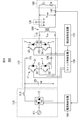
- FIG. 1 is a diagram illustrating a configuration of a power supply system according to the first embodiment.
- FIG. 2 is a diagram illustrating an example of a configuration of a power supply system equivalent to the power supply system of FIG.
- FIG. 3 is a diagram illustrating the flow of current in the inverter unit in the power supply system according to the first embodiment.
- FIG. 4A shows the first relationship between the switching signal of the second switch and the third switch, the voltage applied to the first capacitor, and the current output from the inverter unit in the power supply system according to the first embodiment. It is a figure explaining the example of.
- FIG. 4A shows the first relationship between the switching signal of the second switch and the third switch, the voltage applied to the first capacitor, and the current output from the inverter unit in the power supply system according to the first embodiment. It is a figure explaining the example of.
- FIG. 4A shows the first relationship between the switching signal of the second switch and the third switch, the voltage applied to the first capacitor, and the current output from the inverter unit in
- FIG. 4B shows a second relationship between the switching signal of the second switch and the third switch, the voltage applied to the first capacitor, and the current output from the inverter unit in the power supply system according to the first embodiment. It is a figure explaining the example of.
- FIG. 5 is a diagram illustrating an example of a voltage applied to the smoothing capacitor in the power supply system according to the first embodiment.
- FIG. 6A is a diagram illustrating a first example of an operation simulation result of the power supply system in the power supply system according to the first embodiment.
- FIG. 6B is a diagram illustrating a second example of the operation simulation result of the power supply system in the power supply system according to the first embodiment.
- FIG. 7 is a diagram showing, in a tabular form, simulation results of the power system of the invention example and the power system of the comparative example.
- FIG. 8 is a diagram illustrating a configuration of a power supply system according to the second embodiment.
- FIG. 9 is a diagram illustrating a configuration of a power supply system according to the third embodiment.
- FIG. 10 is a diagram illustrating the flow of current in the inverter unit in the power supply system according to the third embodiment.
- FIG. 11A is a diagram illustrating a first example of the relationship among the switching signal of the first switch, the voltage applied to the high-side capacitor, the voltage applied to the low-side capacitor, and the current output from the inverter unit.
- FIG. 11B is a diagram illustrating a second example of the relationship among the switching signal of the first switch, the voltage applied to the high-side capacitor, the voltage applied to the low-side capacitor, and the current output from the inverter unit.
- FIG. 1 is a diagram illustrating a configuration of a power supply system 100 according to the first embodiment.
- the power supply system 100 includes a DC power supply unit 110, an inverter unit 120, a quasi-resonant element 130, a current transformer 140, a switch control device 150, a current control device 160, and a frequency setting device 170.
- each configuration of the power supply system 100 may be distributed and connected by being communicably connected via a communication unit.
- the power supply system 100 does not have a specific device (vibration suppression circuit) for suppressing the oscillating current.
- the DC power supply unit 110 supplies DC power to the inverter unit 120.
- the DC power supply unit 110 includes an AC power supply 111, a rectifier 112, and a reactor 113.
- the AC power supply 111 outputs AC power.
- An AC power supply 111 is connected to the input terminal of the rectifier 112.
- One end of the reactor 113 is connected to one end on the output side of the rectifier 112.
- the rectifier 112 rectifies AC power supplied from the AC power supply 111 and outputs DC power.
- the rectifier 112 for example, a thyristor rectifier is used. However, the rectifier 112 is not limited to this.
- the rectifier 112 may be configured using a diode rectifier and a voltage control circuit (such as a step-up / step-down chopper).
- the reactor 113 is for smoothing the waveform of the DC power output from the rectifier 112.
- the DC power supply unit 110 is configured to convert AC power into DC power.
- the DC power supply unit 110 is not limited to this.
- the DC power supply unit 110 may be a power supply device that directly supplies a DC current.
- the DC power supply unit 110 may be configured using a battery, a current control circuit, and the like.
- the inverter unit 120 converts the DC power output from the DC power source unit 110 into AC power having the same frequency as the switching frequency for switching each switch of the inverter unit 120. Then, the inverter unit 120 supplies AC power of the frequency to the inductive load 180.
- the inverter unit 120 includes a magnetic energy recovery switch (MERS). An example of the configuration of the inverter unit 120 (magnetic energy regeneration switch) of the present embodiment will be described.
- the inverter unit 120 includes a first switch U, a second switch X, a third switch V, a fourth switch Y, a first AC terminal 121, a second AC terminal 122, a first DC terminal 123, It has a second DC terminal 124 and a first capacitor 125.
- the first switch U, the second switch X, the third switch V, and the fourth switch Y will be described.
- the first switch U, the second switch X, the third switch V, and the fourth switch Y have the same configuration.
- the first switch U, the second switch X, the third switch V, and the fourth switch Y constitute a full bridge circuit.
- the first switch U has a self-extinguishing element S1 and a free-wheeling diode D1.
- the second switch X has a self-extinguishing element S2 and a free wheeling diode D2.
- the third switch V has a self-extinguishing element S3 and a free-wheeling diode D3.
- the fourth switch Y has a self-extinguishing element S4 and a free wheeling diode D4.
- the self-extinguishing elements S1 to S4 can be switched between a state in which a current can flow and a state in which a current cannot flow by an external signal.
- the free-wheeling diodes D1 to D4 have a first end and a second end.
- the free-wheeling diodes D1 to D4 are in a conductive state and pass current from the first end portion to the second end portion, but only have a state in which no current passes from the second end portion to the first end portion. .
- the direction from the first end to the second end of the free-wheeling diodes D1 to D4 is the forward direction in the free-wheeling diodes D1 to D4.
- the first ends of the free-wheeling diodes D1 to D4 are assumed to be ends on the forward direction side.
- the second ends of the free-wheeling diodes D1 to D4 are the ends opposite to the forward direction.
- the self-extinguishing elements S1 to S4 have a first end and a second end.
- the self-extinguishing elements S1 to S4 pass current from the first end to the second end when the current can flow.
- the self-extinguishing elements S1 to S4 do not pass current from the first end to the second end when the current cannot flow.
- the self-extinguishing elements S1 to S4 do not pass current from the second end portion to the first end portion in any state.
- the direction from the first end to the second end of the self-extinguishing elements S1 to S4 is the forward direction in the self-extinguishing elements S1 to S4.
- the first ends of the self-extinguishing elements S1 to S4 are defined as the ends on the forward direction side.
- the second ends of the self-extinguishing elements S1 to S4 are the ends opposite to the forward direction.
- the self-extinguishing elements S1 to S4 are not limited to bipolar transistors.
- the self-extinguishing elements S1 to S4 may be a field effect transistor (FET), an insulated gate bipolar transistor (IGBT), an electron injection promoting gate transistor (IEGT), a gate turn-off thyristor (GTO thyristor), or a gate commutation type turn-off thyristor. (GCT thyristor) can be employed.
- the self-extinguishing element S1 and the freewheeling diode D1 are connected in parallel so that the forward directions are opposite to each other. The same applies to the self-extinguishing element S2 and the freewheeling diode D2, the self-extinguishing element S3 and the freewheeling diode D3, and the self-extinguishing element S4 and the freewheeling diode D4.
- connection point between the forward end of the free-wheeling diodes D1, D2, D3, and D4 and the end opposite to the forward direction of the self-extinguishing elements S1, S2, S3, and S4 is a negative terminal.
- a connection point between the forward end of the self-extinguishing elements S1, S2, S3, and S4 and the end opposite to the forward direction of the freewheeling diodes D1, D2, D3, and D4 is a positive terminal.
- the negative terminal of the first switch U and the positive terminal of the second switch X are connected to each other.
- the positive terminal of the first switch U and the positive terminal of the third switch V are connected to each other.
- the negative terminal of the fourth switch Y and the negative terminal of the second switch X are connected to each other.
- the positive terminal of the fourth switch Y and the negative terminal of the third switch V are connected to each other.
- the first AC terminal 121 is connected to a connection point between the negative terminal of the first switch U and the positive terminal of the second switch X.
- the second AC terminal 122 is connected to a connection point between the negative terminal of the third switch V and the positive terminal of the fourth switch Y.
- the first AC terminal 121 and the second AC terminal 122 are the output ends of the inverter unit 120.
- the first DC terminal 123 is connected to a connection point between the positive terminal of the first switch U and the positive terminal of the third switch V.
- the other end of the reactor 113 is connected to the first DC terminal 123.
- the second DC terminal 124 is connected to a connection point between the negative terminal of the second switch X and the negative terminal of the fourth switch Y.
- the other end on the output side of the rectifier 112 is connected to the second DC terminal 124.
- the first DC terminal 123 and the second DC terminal 124 are input terminals of the inverter unit 120.
- the DC power supply unit 110 is connected between the first DC terminal 123 and the second DC terminal 124.
- the return diodes D1, D2, D3, and D4 are not necessarily provided.
- the self-extinguishing elements S1, S2, S3, and S4 may not be provided.
- the first switch U, the second switch X, the third switch V, and the fourth switch Y may be metal oxide semiconductor field effect transistors (MOS transistors) in which parasitic diodes are built. .
- the first capacitor 125 is connected between the first DC terminal 123 and the second DC terminal 124. That is, one end of the first capacitor 125 and the first DC terminal 123 are connected to each other. The other end of the first capacitor 125 and the second DC terminal 124 are connected to each other.
- the first capacitor 125 is a capacitor having polarity.
- the quasi-resonant element 130 is used to apparently reduce the inductance of the inductive load 180 as viewed from the output end of the inverter unit 120.
- the quasi-resonant element 130 is composed of at least one passive element including a second capacitor.
- the quasi-resonant element 130 is composed of a second capacitor.
- the second capacitor is a nonpolar capacitor.
- the quasi-resonant element 130 is connected in series with the inductive load 180 between the first AC terminal 121 and the second AC terminal 122 of the inverter unit 120. In the example shown in FIG. 1, one end of the quasi-resonant element 130 and the second AC terminal 122 of the inverter unit 120 are connected to each other.
- Inductive load 180 is connected in series with first capacitor 125 between first AC terminal 121 and second AC terminal 122 of inverter unit 120.
- one end of the inductive load 180 and the other end of the quasi-resonant element 130 are connected to each other.
- the other end of the inductive load 180 and the first AC terminal 121 of the inverter unit 120 are connected to each other.
- the inductive load 180 is connected between the first AC terminal 121 and the second AC terminal 122.
- the quasi-resonant element 130 is connected in series with the inductive load 180 between the first AC terminal 121 and the second AC terminal 122.
- the inductive load 180 is a load having an inductance component. It is assumed that the inductive reactance of the inductive load 180 is larger than the capacitive reactance of the inductive load 180. In order to simplify the description, in the following description, it is assumed that the capacitive reactance of the inductive load 180 is 0 (zero).
- the inductive load 180 is, for example, a coil for heating an object to be heated such as a steel plate and an object to be heated.
- the coil that induction-heats the object to be heated of the inductive load 180 generates magnetic lines when an alternating current is supplied from the inverter unit 120. Due to the magnetic lines of force, an eddy current flows through the object to be heated.
- Inductive load 180 is not limited to a coil for induction heating of an object to be heated.
- the inductive load 180 may be a plurality of metal plates (for example, steel plates) subjected to resistance spot welding.
- the plurality of metal plates serving as the inductive load 180 are heated by energization.
- the current transformer 140 measures the alternating current value flowing through the inductive load 180.
- the frequency setting device 170 sets a switching frequency for switching the first switch U, the second switch X, the third switch V, and the fourth switch Y.
- a frequency suitable for induction heating of the object to be heated is set as the switching frequency.
- the frequency suitable for induction heating of the object to be heated is determined based on, for example, the conditions including the specifications of the induction heating device and the shape, width, thickness, and heating temperature of the object to be heated.
- the worker can set the switching frequency when the specification of the induction heating device and the shape, width, thickness, and heating temperature of the object to be heated are different as frequencies suitable for induction heating of the object to be heated.
- the frequency setting device 170 can store the frequency thus investigated in a storage device such as a ROM in advance. Further, the frequency setting device 170 can also input information on the switching frequency based on the operation of an operator via an input interface such as a screen for inputting the frequency.
- the switch control device 150 generates a switching signal for switching the first switch U, the second switch X, the third switch V, and the fourth switch Y at the switching frequency set by the frequency setting device 170. To do. Then, the switch control device 150 outputs a switching signal to the first switch U, the second switch X, the third switch V, and the fourth switch Y. Based on this switching signal, the conduction states of the self-extinguishing elements S1, S2, S3, and S4 of the first switch U, the second switch X, the third switch V, and the fourth switch Y are switched.
- ON a state in which the self-extinguishing elements S1, S2, S3, and S4 can pass a current
- OFF A state where the self-extinguishing elements S1, S2, S3, and S4 cannot flow current.
- the switch control device 150 When the first switch U and the fourth switch Y are on, the switch control device 150 turns off the second switch X and the third switch V. Further, the switch control device 150 turns on the second switch X and the third switch V when the first switch U and the fourth switch Y are OFF. In addition, the switch control device 150 turns on and off each of the first switch U, the second switch X, the third switch V, and the fourth switch Y at the switching frequency set by the frequency setting device 170. Switch. Note that the frequency of the current I inv output from the inverter unit 120 is set as a switching frequency (details of this point will be described later). In this embodiment, the switching frequency for switching the first switch U, the second switch X, the third switch V, and the fourth switch Y is the output frequency of the magnetic energy regeneration switch.
- f be a switching frequency at which the switch control device 150 switches the first switch U, the second switch X, the third switch V, and the fourth switch Y.
- the inverter unit 120 supplies the current I inv having the frequency f to the inductive load 180.
- the current control device 160 monitors the current measured by the current transformer 140. Then, the current control device 160 controls the operation of the rectifier 112 so that the current measured by the current transformer 140 becomes a target value.
- the target value is determined based on the physical property value, the size, etc. of the object to be heated.
- the physical property values include, for example, magnetic permeability and resistivity.
- the angular frequency ⁇ [rad / s] is expressed by 2 ⁇ f using the frequency f [Hz].
- L be the inductance of the inductive load 180.
- L ′ be the apparent inductance of the inductive load.
- the capacitance of the second capacitor quasi-resonant elements 130 and C r is expressed by the following equation (1).
- the circuit configuration of the power supply system 100 is a circuit in which an inductive load having an inductance L ′ shown in the equation (2) is connected between the first AC terminal 121 and the second AC terminal 122 of the inverter unit 120.
- FIG. 2 is a diagram illustrating an example of a configuration of a power supply system equivalent to the power supply system 100 of FIG.
- FIG. 2 is a diagram in which an apparent inductive load 210 is arranged instead of the quasi-resonant element 130 and the inductive load 180 shown in FIG.
- the power supply system 200 includes an apparent inductive load 210 that does not include the pseudo-resonant element 130 and has an inductance L ′.
- the power supply system 200 shown in FIG. 2 is different from the power supply system 100 shown in FIG.
- the power supply system 200 shown in FIG. 2 is equivalent to the power supply system 100 shown in FIG. That is, the power supply system 100 according to the present embodiment has the quasi-resonant element 130 connected in series with the inductive load 180, so that the inductance of the inductive load 180 is apparently reduced.
- FIG. 3 is a diagram illustrating an example of a current flow in the inverter unit 120.
- 4A shows the relationship between the switching signal V-X gate of the second switch X and the third switch V, the voltage V mersc applied to the first capacitor 125, and the current I inv output from the inverter unit 120.
- FIG. It is a figure explaining a 1st example.
- 4B shows the relationship between the switching signal V-X gate of the second switch X and the third switch V, the voltage V mersc applied to the first capacitor 125, and the current I inv output from the inverter unit 120. It is a figure explaining a 2nd example.
- V-X gate is a signal that the switch control device 150 transmits to the second switch X and the third switch V, and is an ON / OFF switching signal for the second switch X and the third switch V. It is.
- the second switch X and the third switch V are in the ON state when the switching signal VX gate indicates the ON value, and the second switch X and the third switch V are in the ON state when the switching signal VX gate indicates the OFF value.
- the switch X and the third switch V are OFF.
- the switch control device 150 also transmits a switching signal U-Y gate to the first switch U and the fourth switch Y.
- the value of the switching signal UY gate indicates a value opposite to the switching signal transmitted to the second switch X and the third switch V. That is, the value of the switching signal U-Y Gate, showed a value of OFF when the switching signal V-X Gate has a value of ON, indicating the value of ON when the switching signal V-X Gate has a value of OFF .
- V mersc indicates a voltage applied to the first capacitor 125.
- I inv represents a current output from the inverter unit 120.
- t 0 indicates the time at which the first capacitor 125 starts discharging.
- the current I inv output from the inverter unit 120 increases in the positive direction, and the voltage V mersc applied to the first capacitor 125 starts to decrease.
- the voltage V mersc applied to the first capacitor 125 becomes 0 (zero).
- t 1 indicates the time when the first capacitor 125 completes discharging.
- the current I inv output from the inverter unit 120 reaches a peak, and the voltage V mersc of the first capacitor 125 becomes 0 (zero). Since the voltage between the first DC terminal 123 and the second DC terminal 124 is 0 (zero), no current flows between the first DC terminal 123 and the second DC terminal 124. In this case, as in the state B in FIG. 3, a part of the current flowing into the first AC terminal 121 is directed to the first DC terminal 123 via the free wheel diode D1 of the first switch U, 3 to the second AC terminal 122 via the switch V.
- the remainder of the current flowing into the first AC terminal 121 is directed to the second DC terminal 124 via the second switch X, and then passed through the free-wheeling diode D4 of the fourth switch Y. Go to AC terminal 122.
- the voltage V mersc applied to the first capacitor 125 is 0 (zero). Therefore, the voltages applied to the first switch U, the second switch X, the third switch V, and the fourth switch Y are also 0 (zero).
- a period in which the voltage V mersc applied to the first capacitor 125 is 0 (zero) is defined as T 0 .
- the current flowing through the inverter unit 120 and the inductive load 180 gradually decreases according to a time constant determined from the inductance and resistance components of the inductive load 180.
- the current I inv output from the inverter unit 120 decreases during the period from time t 1 to time t 2 .
- the switch control device 150 turns on the first switch U and the fourth switch Y at the time t 2 when the period T 0 has elapsed from the time t 1 when the discharge of the first capacitor 125 is completed, and the second switch X and the third switch V are switched OFF. At this time, since the voltage V mersc applied to the first capacitor 125 is 0 (zero), soft switching is performed. Soft switching means that the switch is switched from ON to OFF or from OFF to ON when the voltage applied to the switch is theoretically 0 (zero).
- the first switch U and the fourth switch Y When the first switch U and the fourth switch Y are switched ON and the second switch X and the third switch V are switched OFF, the first switch U and the fourth switch Y flow into the first AC terminal 121 as in the state C of FIG. Since the second switch X is OFF, the current cannot flow to the second switch X, and goes to the first DC terminal 123 via the first switch U. The current flowing into the first DC terminal 123 cannot flow through the third switch V because the third switch V is OFF, and is directed to the first capacitor 125. The current flowing into the first capacitor 125 is used for charging the first capacitor 125 and gradually decreases. This current flows as in state C in FIG. 3 until the first capacitor 125 completes charging, and becomes 0 (zero) when charging of the first capacitor 125 is completed. In Figure 4A, the first capacitor 125, and to complete the charging time t 3.
- the voltage V mersc applied to the first capacitor 125 rises between time t 2 and time t 3 . Further, the current I inv output from the inverter unit 120 decreases as the voltage V mersc applied to the first capacitor 125 increases. When the charging of the first capacitor 125 is completed at time t 3, the voltage V Mersc of the first capacitor 125 reaches a peak. At this time, the current I inv output from the inverter unit 120 is 0 (zero).
- the first capacitor 125 After the charging of the first capacitor 125 is completed, the first capacitor 125 starts discharging. As in state D in FIG. 3, the current discharged from the first capacitor 125 is directed to the first DC terminal 123. Since the first switch U is ON and the third switch V is OFF, the current flows to the first AC terminal 121 via the first switch U, and the inductive load 180 and the pseudo-current. It flows into the resonant element 130. The current flowing into the quasi-resonant element 130 goes to the second AC terminal 122, goes to the first capacitor 125 via the fourth switch Y and the second DC terminal 124.
- the inverter unit 120 has the switching frequency f set by the switch control device 150, and the first switch U, the second switch X, the third switch V, and the fourth switch Y are turned on and off. Is switched to output a current I inv having the same frequency as the switching frequency f.
- the first capacitor 125 At time t 4, to complete the discharge.
- the voltage V mersc applied to the first capacitor 125 continues to decrease from time t 3 in accordance with the discharge of the first capacitor 125, and becomes 0 (zero) at time t 4 .
- the current I inv output from the inverter unit 120 increases in the direction opposite to the direction from time t 0 to time t 3 in accordance with the discharge of the first capacitor 125.
- the current I inv output from the inverter unit 120 reaches a peak in a direction opposite to the direction from time t 0 to time t 3 at time t 4 when the discharge of the first capacitor 125 is completed.
- the direction of the current I inv output from the inverter unit 120 between time t 3 and time t 4 is opposite to the direction of the current I inv output from the inverter unit 120 between time t 0 and time t 1. .
- the value of the current I inv output from the inverter unit 120 between time t 3 and time t 4 is a negative value.
- the discharge of the first capacitor 125 is completed, the voltage V Mersc of the first capacitor 125 becomes 0 (zero). Since the voltage between the first DC terminal 123 and the second DC terminal 124 is 0 (zero), between the first DC terminal 123 and the second DC terminal 124 as in the state E in FIG. No current flows. In this case, a part of the current flowing into the second AC terminal 122 is directed to the first DC terminal 123 via the free-wheeling diode D3 of the third switch V, via the first switch U, Go to the first AC terminal 121. The remainder of the current flowing into the second AC terminal 122 goes to the second DC terminal 124 via the fourth switch Y, passes through the free wheel diode D2 of the second switch X, and passes through the first current. Head to AC terminal 121.
- the current flowing through the inverter unit 120 and the inductive load 180 gradually approaches 0 (zero) according to the time constant due to the inductance and resistance components of the inductive load 180.
- the current I inv output from the inverter unit 120 approaches 0 (zero) during the period from time t 4 to time t 5 .
- Switch controller 150 at time t 5 has elapsed period T 0 from time t 4 when the discharge of the first capacitor 125 is completed, switching the first switch U and the fourth switch Y to OFF, the second Switch X and third switch V are turned ON. At this time, since the voltage V mersc applied to the first capacitor 125 is 0 (zero), soft switching is performed.
- the voltage V mersc applied to the first capacitor 125 rises between time t 5 and time t 6 . Further, the current I inv output from the inverter unit 120 approaches 0 (zero) as the voltage V mersc applied to the first capacitor 125 increases. When the charging of the first capacitor 125 is completed at time t 6, the voltage V Mersc of the first capacitor 125 reaches a peak. At this time, the current I inv output from the inverter unit 120 is 0 (zero).
- the first capacitor 125 has completed charging, since the first switch U and the fourth switch Y is OFF, the second switch X, and the third switch V is in ON, initial Return to state A, which is the state.
- the inverter unit 120 repeats the above operation.
- the first capacitor 125 when the first capacitor 125 is charged, current flows from the first DC terminal 123 into the first capacitor 125. In other words, the first capacitor 125 always accumulates positive charges on the first DC terminal 123 side and negative charges on the second DC terminal 124 side. For this reason, a capacitor having polarity can be used as the first capacitor 125. Further, the direction of the current flowing into the second capacitor included in the quasi-resonant element 130 is not constant. For this reason, a capacitor having polarity cannot be used as the second capacitor, and a nonpolar capacitor is used.
- a current corresponding to one cycle of the alternating current is output as the current I inv output from the inverter unit 120. That is, the inverter unit 120 outputs an alternating current having the same frequency as the switching frequency f.
- FIG. 4A shows a case where the period T 0 during which the voltage V mersc applied to the first capacitor 125 remains 0 (zero) exceeds 0 (zero).
- FIG. 4B shows a case where the period T 0 during which the voltage V mersc applied to the first capacitor 125 remains 0 (zero) is 0 (zero).
- an example of the operation of the inverter unit 120 when the period T 0 during which the voltage V mersc applied to the first capacitor 125 remains 0 (zero) is 0 (zero) will be described with reference to FIGS. 3 and 4B. While explaining.
- the first capacitor 125 is charged, the first switch U and the fourth switch Y are OFF, and the second switch X and the third switch V are ON.
- the first capacitor 125 is time t 0 to time t as shown in FIG. 4B. to discharge to t 1. Then, the voltage V Mersc of the first capacitor 125 at time t 1 is 0 (zero).
- the operation of the inverter unit 120 from time t 0 to time t 1 shown in FIG. 4B is the same as the operation of the inverter unit 120 from time t 0 to time t 1 shown in FIG. 4A.
- a period T 0 in which the voltage V mersc applied to the first capacitor 125 remains 0 (zero) after time t 1 is provided.
- the period T 0 during which the voltage V mersc applied to the first capacitor 125 remains 0 (zero) is 0 (zero).
- the first capacitor 125 is charged between time t 1 and time t 2 and discharged between time t 2 and time t 3 .
- the voltage V mersc applied to the first capacitor 125 becomes 0 (zero).
- the first switch U, the second switch X, the third switch V, and the fourth switch Y transition from the state A in FIG. Do not take.
- the operation of the inverter unit 120 between time t 1 and time t 3 shown in FIG. 4B is the same as the operation of the inverter unit 120 between time t 2 and time t 4 shown in FIG. 4A.
- a period T 0 in which the voltage V mersc applied to the first capacitor 125 remains 0 (zero) is provided.
- the period T 0 during which the voltage V mersc applied to the first capacitor 125 remains 0 (zero) is 0 (zero).
- the first capacitor 125 is charged between time t 3 and time t 4 .
- the first switch U, the second switch X, the third switch V, and the fourth switch Y transition from the state D to the state F in FIG. Do not take.
- the operation of the inverter unit 120 between time t 3 and time t 4 shown in FIG. 4B is the same as the operation of the inverter unit 120 between time t 5 and time t 6 shown in FIG. 4A.
- the current I inv output from the inverter unit 120 increases in the positive direction from time t 0 as the first capacitor 125 is discharged. Then, the current I inv output from the inverter unit 120 reaches a peak at time t 1 when the discharge of the first capacitor 125 is completed. The current I inv output from the inverter unit 120 approaches 0 (zero) as the first capacitor 125 is charged from time t 1 . The current I inv output from the inverter unit 120 becomes 0 (zero) at time t 2 when the charging of the first capacitor 125 is completed.
- the current I inv output from the inverter unit 120 reaches a peak in a direction opposite to the direction from the time t 0 to the time t 2 at the time t 3 when the discharge of the first capacitor 125 is completed.
- the current I inv output from the inverter unit 120 approaches 0 (zero) as the first capacitor 125 is charged from time t 3 .
- the current I inv output from the inverter unit 120 becomes 0 (zero) at time t 4 when the charging of the first capacitor 125 is completed.
- the switch control device 150 includes the first switch U, the fourth switch Y, and the second switch X.
- the third switch V is switched on and off. In this way, the switch control device 150 can realize soft switching even when the period T 0 in which the voltage V mersc applied to the first capacitor 125 remains 0 (zero) is 0 (zero). .
- the period related to the charging and discharging of the first capacitor 125, the capacitance C m of the first capacitor 125, in a half cycle of the resonance frequency determined from the inductance L 'of the inductive load 210 apparent is there.
- the current I inv output from the inverter unit 120 Is equal to the resonance frequency determined from the capacitance of the first capacitor 125 and the apparent inductance L ′ of the inductive load 210.
- the first switch U, the second switch Y, the second switch X, and the third switch V are turned on and off to switch the first switch U, second switch
- the first capacitor 125 and the quasi-resonant element 130 are arranged in series on the path of the alternating current that flows through all or part of the switch X, the third switch V, and the fourth switch Y.
- this alternating current is not shunted in the inverter unit 120 except in the state B and the state E shown in FIG.
- the inverter unit 120, the quasi-resonant element 130, and the inductive load 180 are The capacitor 125, the quasi-resonant element 130, and the inductive load 180 having an inductance L can be regarded as a series resonant circuit. Further, the quasi-resonant element 130 and the inductive load 180 are equivalent to the apparent inductive load 210 having the inductance L ′.
- the series resonance circuit in which the inverter unit 120, the quasi-resonant element 130, and the inductive load 180 are connected in series has a series resonance in which the first capacitor 125 and the apparent inductive load 210 are connected in series. It can be regarded as a circuit.
- the first capacitor 125, the apparent inductive load 210, and the resonance frequency f res determined from the capacitance C m of the first capacitor 125 and the inductance L ′ of the apparent inductive load 210. Resonates.
- L ′ ⁇ C m needs to be a positive real number.
- the capacitance C m of the first capacitor 125 is a positive value because it is a scalar value. Therefore, in order for L ′ ⁇ C m to be a positive real number, the apparent inductance L ′ of the inductive load 210 needs to be a positive value (that is, a value exceeding 0 (zero)).
- the switch control device 150 realizes soft switching by switching ON / OFF of the first switch U and the fourth switch Y and the second switch X and the third switch V at this timing. Can do.
- the switch control device 150 can adjust the frequency of the voltage I inv output from the inverter unit 120 by adjusting the period in which the voltage V mersc applied to the first capacitor 125 is 0 (zero). .
- the first switch U and the fourth switch Y and the second switch X and the third switch V are turned on and off.
- the period up to the time when the switching is performed is the same as the period T 0 in which the voltage V mersc applied to the first capacitor 125 is 0 (zero). Then, the following relational expression (3) is established.
- one period of the resonance frequency f res is expressed by the following equation (4).
- the period T 0 during which the voltage V mersc applied to the first capacitor 125 is 0 (zero) is a value equal to or greater than 0 (zero). Therefore, one period of the resonance frequency f res determined from the capacitance C m of the first capacitor 125 and the apparent inductance L ′ of the inductive load 210 is equal to or less than one period of the switching frequency f of the inverter unit 120. Become. That is, the resonance frequency f res determined from the capacitance C m of the first capacitor 125 and the apparent inductance L ′ of the inductive load 210 needs to be larger than the switching frequency f. Therefore, the capacitance C m of the first capacitor 125 needs to be a value that satisfies the following equation (5).
- the inverter unit 120 does not generate a case where the voltage V mersc applied to the first capacitor 125 becomes 0 (zero). Switching becomes impossible.
- the switching frequency f of the inverter unit 120 is set to be equal to or lower than the resonance frequency f res in the resonance circuit including the first capacitor 125, the pseudo resonance element 130, and the inductive load 180.
- the switching frequency of the inverter unit 120 is f
- the first capacitor 125, the quasi-resonant element 130, the induction that satisfies L ′> 0 and the expression (5) is satisfied. It is necessary to have a sexual load 180.
- ⁇ (L ′ ⁇ C m ) is a positive value.
- the capacitance C m of the first capacitor 125 has a positive value. Therefore, the relational expression of L ′> 0 is also satisfied.
- the power supply system 100 includes the first capacitor 125, the quasi-resonant element 130, and the inductive load 180 that satisfy the expression (5) when the switching frequency of the inverter unit 120 is f. It will be good.
- the power supply system 100 reduces the apparent inductance of the inductive load 180 viewed from the inverter unit 120, thereby reducing the apparent reactance of the inductive load 180, and outputs from the inverter unit 120.
- the applied voltage V inv can be reduced. If the currents output from the inverter unit 120 are the same, the capacity of the inverter unit 120 may be smaller when the quasi-resonant element 130 is provided than when the quasi-resonant element 130 is not provided.
- the power supply system 100 causes the first capacitor 125 and the apparent inductive load 210 to resonate at a frequency equal to or higher than the switching frequency f of the inverter unit 120, thereby causing the voltage V applied to the first capacitor 125.
- a period when mersc is 0 (zero) can be generated.
- the power supply system 100 can implement
- the power supply system 100 includes the first capacitor 125, the quasi-resonant element 130, and the inductive load 180 that satisfy the expression (5) at all possible frequencies as the switching frequency f of the inverter unit 120. To. By doing in this way, the power supply system 100 can reduce the voltage V inv output from the inverter unit 120 (that is, the inverter unit 120) even when the switching frequency f of the inverter unit 120 is changed by the switch control device 150. (Capacity reduction) and soft switching can be realized.
- the quasi-resonant element 130 is connected in series with the inductive load 180 instead of in parallel. Further, there is no capacitor (passive element having a capacitive reactance) connected in parallel with the inductive load 180 on the inductive load 180 side of the inverter unit 120. Therefore, the quasi-resonant element 130 and the inductive load 180 do not constitute a closed circuit. Therefore, no oscillating current is generated. Therefore, an unexpected current can be prevented from flowing into the inductive load 180. From the above, the inverter unit 120 can transmit a desired current in which vibration is suppressed to the inductive load 180 without using a specific device such as a vibration suppression circuit.
- the inverter unit 120 performs ON / OFF switching of the first switch U and the fourth switch Y and the second switch X and the third switch V as described above. Therefore, the inverter unit 120 collects the magnetic energy stored in the inductive load 180, stores it as electrostatic energy, charges the first capacitor 125, and stores the electrostatic energy stored in the first capacitor 125. Is repeatedly supplied to the inductive load 180. Therefore, the voltage V mersc applied to the first capacitor 125 is an AC voltage including a period of 0 (zero) as shown in FIGS. 4A and 4B. That is, the first capacitor 125 is not for smoothing the waveform of the DC power output from the rectifier 112.
- the voltage applied to the first capacitor 125 may vary due to pulsating current. as shown in FIG. 5, substantially becomes constant value E d, it does not take a value of 0 (zero). Furthermore, in this case, it is necessary to resonate only with the quasi-resonant element 130 and the inductive load 180. However, under the condition shown in the equation (5), the quasi-resonant element 130 and the inductive load 180 alone do not resonate.
- V inv The voltage output from the inverter unit 120
- the current output from the inverter unit 120 is I inv
- the voltage applied to the pseudo-resonant element 130 is V r
- the voltage applied to the inductive load 180 is V load .
- the capacity of the inverter unit 120 is I inv ⁇ V inv .
- the voltage V inv output from the inverter unit 120 is expressed by the following equation (7).
- the voltage V inv output from the inverter unit 120 decreases as the capacitance C m of the first capacitor 125 increases.
- first capacitor 125 In the state that the voltage depends on the first capacitor 125, first capacitor 125, a quasi-resonant element 130 and the inductive load 180, resonates at a resonant frequency f res (For the resonance frequency f res (5) formula See).
- the resonance frequency f res does not change, the inductance L ′ decreases as the capacitance C m of the first capacitor 125 increases. Since the inductance L ′ is expressed by the following equation (8), the inductance L ′ decreases as the electrostatic capacitance C r of the second capacitor of the quasi-resonant element 130 decreases.
- the switch control device 150 sets the first switch U and the fourth switch Y, the second switch X, and the third switch V to 9.9 [kHz] to 7.0 [kHz]. Switching is performed at the switching frequency f. In this case, the frequency of the current I inv output from the inverter unit 120 is 9.9 [kHz] to 7.0 [kHz].
- the capacitance C r of the second capacitor of the quasi-resonant element 130 is 30 [ ⁇ F].
- resonance is caused by the apparent inductive load 210 having a combined reactance of the quasi-resonant element 130 and the inductive load 180 and the first capacitor 125.
- this resonance can be regarded as a resonance between the inductive load 180 and the capacitor having the combined capacitance of the first capacitor 125 and the pseudo-resonant element 130 as the capacitance.
- a capacitor having a combined capacitance of the first capacitor 125 and the pseudo-resonant element 130 as a capacitance is assumed.
- this capacitor is referred to as a synthetic capacitor.
- C res be the capacitance of the composite capacitor. Then, since the electrostatic capacity C res of the composite capacitor resonates with the inductance L of the inductive load 180, the following equation (9) is obtained.
- the capacitance C res of the composite capacitor when the frequency of the current I inv output from the inverter 120 is 9.9 [kHz] is about 10 [ ⁇ F] ( ⁇ 1 / ((2 ⁇ ⁇ 9.9 ⁇ 10 3 ) 2 ⁇ 23.7 ⁇ 10 ⁇ 6 )
- the first capacitor 125 and the fourth switch Y, and the second switch X and the third switch V are switched on and off so that soft switching is performed. What is necessary is just to design the electrostatic capacitance Cm.
- the period T 0 during which the voltage V mersc applied to the first capacitor 125 remains 0 (zero) can be expressed by the following equation (13) from the equation (3).
- f res is a resonance frequency determined from the capacitance C m of the first capacitor 125 and the apparent inductance L ′ of the inductive load 210. From this equation (13), the resonance frequency f res is expressed by the following equation (14), which is approximately 10.4 [kHz] ( ⁇ 1 / (1 / 9.9 ⁇ 10 3 ⁇ 2 ⁇ (2.5 ⁇ 10 ⁇ 6 )).
- the angular frequency ⁇ res when the frequency is the resonance frequency f res determined from the capacitance C m of the first capacitor 125 and the apparent inductance L ′ of the inductive load 210 is 15)
- ⁇ res 2 ⁇ f res (15) Since the capacitance C m of the first capacitor 125 resonates with the apparent inductance L ′ of the inductive load 210, the following equation (16) is established.
- the angular frequency ⁇ when the frequency is the switching frequency f of the inverter unit 120 is 2 ⁇ ⁇ 7.0 ⁇ 10 3 [rad / s].
- the inductance L of the inductive load 180 when the switching frequency f of the inverter unit 120 is 7.0 [kHz] is 24.2 [ ⁇ H].
- the capacitance C r of the second capacitor of the quasi-resonant element 130 is about 21.4 [ ⁇ F] ( ⁇ 1 / ((2 ⁇ ⁇ 7 ⁇ 10 3 ) 2 ⁇ 24.2. ⁇ 10 -6 )) must be exceeded.
- the capacitance C r of the second capacitor quasi-resonant element 130 because it is 30 [microfarads], thereby satisfying the expression (19). That is, since the value of the apparent inductance L ′ of the inductive load 210 is a positive value, the quasi-resonant element 130 and the inductive load 180 resonate with the first capacitor 125.
- the switching frequency f of the inverter unit 120 is higher than 7.0 [kHz]. Even when the switching frequency f is 7.0 [kHz], soft switching can be realized.
- the capacitance C r of the second capacitor of the quasi-resonant element 130 is determined so as to satisfy the equation (18) according to the inductance L of the inductive load 180 and the switching frequency f.
- the capacitance C m of the first capacitor 125 is determined so as to satisfy the equation (17) using the capacitance C r of the second capacitor of the quasi-resonant element 130 thus determined. .
- the capacitance C r of the second capacitor quasi-resonant element 130 for example, 6.5
- An appropriate value is selected from the range of [ ⁇ F] to 250 [ ⁇ F]
- the capacitance C m of the first capacitor 125 is, for example, an appropriate value from the range of 0.06 [ ⁇ F] to 20 [ ⁇ F]. Is selected.
- 6A and 6B are diagrams illustrating an example of an operation simulation result of the power supply system 100 of the present embodiment.
- 6A is a waveform when the switching frequency f of the inverter unit 120 is 9.9 [kHz] and the inductance L of the inductive load 180 is 23.7 [ ⁇ H].
- 6B is a waveform when the switching frequency f of the inverter unit 120 is 7.0 [kHz] and the inductance L of the inductive load 180 is 24.2 [ ⁇ H].
- the waveforms shown in FIGS. 6A and 6B the capacitance C m of the first capacitor 125 is 15 [microfarads], the electrostatic capacitance of the second capacitor quasi-resonant elements 130 C r is 30 [microfarads ].
- I inv represents a current output from the inverter unit 120.
- V inv represents a voltage output from the inverter unit 120.
- V mersc indicates a voltage applied to the first capacitor 125.
- Arms applied to the side of the waveform of the current I inv output from the inverter unit 120 indicates the effective value of the waveform (current I inv ).
- Vrms attached to the side of the waveform of the voltage V inv output from the inverter unit 120 and the voltage V mersc applied to the first capacitor 125 indicates the effective value of the waveform (voltage V inv , V mersc ). .
- U-Y gate indicates a switching signal transmitted from the switch control device 150 to the first switch U and the fourth switch Y.
- the switch control device 150 transmits to the second switch X and the third switch V a switching signal V-X gate opposite to the switching signal indicated by U-Y gate .
- FIG. 7 is a table showing simulation results of the power supply system of the invention example and the power supply system of the comparative example in a table format.
- the power supply system of the example of the invention is the power supply system 100 of the present embodiment.
- the power supply system of the comparative example is obtained by removing the quasi-resonant element 130 from the power supply system 100 of the present embodiment. Except for the presence or absence of the quasi-resonant element 130, there is no difference between the power supply system of the invention example and the power supply system of the comparative example.
- Arms and Vrms shown in FIG. 7 represent effective values as in FIGS. 6A and 6B.
- FIG. 7 shows the results of two simulations in which the switching frequency f of the inverter unit 120 is 9.9 [kHz] and 7.0 [kHz]. Further, the capacitance C m of the first capacitor 125 of each power supply system is 15 [ ⁇ F]. The capacitance C r of the pseudo power supply system of the invention Example resonant element 130 (second capacitor) is 30 [ ⁇ F]. The capacitance of the first capacitor 125 of the power supply system of the comparative example is 9.3 [ ⁇ F]. Further, the inductance L of the inductive load 180 is 23.7 [ ⁇ H] when the switching frequency f is 9.9 [kHz], or 24.2 [ ⁇ H] when the switching frequency f is 7.0 [kHz]. is there. In the simulation, the inverter unit 120 of the invention example and the comparative example output the same current.
- the voltage V inv output from the inverter unit 120 is shown to be smaller in the power supply system 100 of the invention example.
- the capacity of the inverter unit 120 of the power supply system 100 of the invention example is smaller than the capacity of the inverter unit 120 of the power supply system of the comparative example. That is, by using the quasi-resonant element 130, the capacity of the inverter unit 120 of the power supply system can be reduced.
- the quasi-resonant element 130 includes the second capacitor
- the quasi-resonant element 130 only needs to include the second capacitor.
- the second capacitor may be a single capacitor or a plurality of capacitors connected to each other.
- the plurality of capacitors may be connected to each other in series, may be connected to each other in parallel, or a portion connected in series and a portion connected in parallel may be mixed.
- the capacitance C r of the second capacitor quasi-resonant element 130 composite electrostatic of the plurality of capacitors It becomes capacity.
- the quasi-resonant element 130 When the capacitive reactance due to the capacitance of the second capacitor included in the quasi-resonant element 130 is larger than the inductive reactance of the inductive load 180, the quasi-resonant element 130 is added to the second capacitor, You may have a reactor. However, as described in the present embodiment, the value of the inductive reactance on the inductive load 180 side from the output end of the magnetic energy regenerative switch is greater than that on the inductive load 180 side from the output end of the magnetic energy regenerative switch. Above the capacitive reactance value.
- the inductance L of the inductive load 180 may be replaced with a combined inductance of the inductive load 180 and the reactor included in the quasi-resonant element 130. Therefore, the value of the combined reactance of the inductive reactance of the quasi-resonant element 130 and the inductive reactance of the inductive load 180 is set to exceed the value of the capacitive reactance of the quasi-resonant element 130.
- the capacitance C r of the second capacitor satisfies the conditions the combined inductance of the inductance (19) of L of formula, inductance and inductive load 180 of quasi-resonant element 130.
- the first capacitor 125 may be configured using at least one capacitor.
- a plurality of capacitors connected to each other may be used as the first capacitor 125.
- the plurality of capacitors may be connected to each other in series, may be connected to each other in parallel, or a portion connected in series and a portion connected in parallel may be mixed.
- the capacitance C m of the first capacitor 125 is the combined capacitance of the plurality of capacitors.
- a power supply system capable of adjusting the current I inv output from the inverter unit 120
- a transformer is disposed between inverter unit 120, quasi-resonant element 130 and inductive load 180.
- this embodiment adds a transformer with respect to 1st Embodiment. Therefore, in the description of the present embodiment, the same parts as those in the first embodiment are denoted by the same reference numerals as those in FIGS. 1 to 7, and detailed description thereof is omitted. Also in the present embodiment, as in the first embodiment, the case where the quasi-resonant element 130 includes a second capacitor will be described as an example.
- FIG. 8 is a diagram illustrating an example of the configuration of the power supply system 800.
- the power supply system 800 includes a transformer 810 in addition to the DC power supply unit 110, the inverter unit 120, the quasi-resonant element 130, the current transformer 140, the switch control device 150, the current control device 160, and the frequency setting device 170.
- the power supply system 800 does not have a specific device (vibration suppression circuit) for suppressing the oscillating current.
- the transformer 810 boosts or steps down the voltage V inv output from the inverter unit 120.
- One end of the primary winding (input side winding) of transformer 810 and second AC terminal 122 are connected to each other.
- the other end of the primary winding of transformer 810 and first AC terminal 121 are connected to each other.
- One end of the secondary winding (output-side winding) of transformer 810 and one end of quasi-resonant element 130 are connected to each other.
- the other end of the secondary winding of transformer 810 and the other end of inductive load 180 are connected to each other. Note that one end of the inductive load 180 is connected to the other end of the pseudo-resonant element 130.
- the turns ratio of the transformer 810 is n.
- the turns ratio n exceeds 1.
- the turns ratio n is less than 1.
- the transformer 810 is an ideal transformer.
- the primary voltage of transformer 810 (voltage applied to the primary winding) is voltage V inv output from inverter unit 120.
- the primary current of transformer 810 (current flowing through the primary winding) is current I inv output from inverter unit 120.
- the power supply system 800 of the present embodiment can adjust the current flowing through the inductive load 180 by the turns ratio n of the transformer 810.
- a step-down transformer is used as the transformer 810, a large current can flow through the inductive load 180 without flowing a large current through the inverter unit 120. Therefore, for example, it is not necessary to use a large current element as the first switch U, the second switch X, the third switch V, the fourth switch Y, and the first capacitor 125.
- the impedance Z when the inductive load 180 side is viewed from the output terminal of the inverter unit 120 is expressed by the following equation (20).
- R is the resistance [ ⁇ ] of the inductive load 180.
- L is the inductance [H] of the inductive load 180.
- C r is the capacitance [F] of the second capacitor of the quasi-resonant element 130.
- n is the turn ratio of the transformer 810. j is an imaginary unit.
- the equation (12) is established. That is, even if transformer 810, the capacitance C r of the second capacitor quasi-resonant element 130 is determined in the same manner as the first embodiment. From the equation (20), in the present embodiment, the apparent inductance L ′ of the inductive load 210 is expressed by the following equation (22).
- the capacitance C m of the first capacitor 125 may be designed so as to satisfy the equation (23) instead of the equation (17). Also in this embodiment, the modification described in the first embodiment can be adopted.
- FIG. 9 is a diagram illustrating an example of the configuration of the power supply system 900.
- the power supply system 900 includes a DC power supply unit 110, an inverter unit 920, a pseudo resonant element 130, a current transformer 140, a switch control device 150, a current control device 160, and a frequency setting device 170.
- the power supply system 900 does not have a specific device (vibration suppression circuit) for suppressing the oscillating current.
- the inverter unit 920 converts the DC power output from the DC power supply unit 110 into AC power having the same frequency as the switching frequency for switching each switch of the inverter unit 920. Convert to Then, the inverter unit 920 supplies AC power of the frequency to the inductive load 180.
- the inverter unit 920 has a magnetic energy regenerative switch.
- the inverter unit 920 includes a first switch U, a second switch X, a first free-wheeling diode D5, a second free-wheeling diode D6, a first AC terminal 921, second AC terminals 922 and 925, and a first A DC terminal 923, a second DC terminal 924, and a plurality of first capacitors are included.
- the inverter unit 920 includes a high side capacitor 926 and a low side capacitor 927 as a plurality of first capacitors.
- the first switch U is the same as the first switch U described in the first embodiment.
- the second switch X is the same as the second switch X described in the first embodiment. Therefore, detailed description of the first switch U and the second switch X is omitted here.
- the connection point between the forward ends of the free-wheeling diodes D1 and D2 and the ends of the self-extinguishing elements S1 and S2 opposite to the forward direction is a negative terminal.
- a connection point between the end portion on the forward direction side of the self-extinguishing elements S1 and S2 and the end portion on the opposite side to the forward direction of the free-wheeling diodes D1 and D2 is defined as a positive electrode terminal.
- the free-wheeling diodes D5 and D6 have a first end and a second end.
- the free-wheeling diodes D5 and D6 are in a conductive state and have only a state in which current is passed from the first end to the second end but no current is passed from the second end to the first end. .
- the direction from the first end to the second end of the free-wheeling diodes D5 and D6 is the forward direction of the free-wheeling diodes D5 and D6.
- the first ends of the free-wheeling diodes D5 and D6 are used as negative terminals.
- the second ends of the free-wheeling diodes D5 and D6 are used as positive terminals.
- a connection form of each part of the inverter unit 920 will be described.
- the negative terminal of the first switch U and the positive terminal of the second switch X are connected to each other.
- the negative terminal of the first freewheeling diode D5 and the positive terminal of the second freewheeling diode D6 are connected to each other.
- the positive terminal of the first switch U and the positive terminal of the first freewheeling diode D5 are connected to each other.
- the negative terminal of the second switch X and the negative terminal of the second freewheeling diode D6 are connected to each other.
- the first AC terminal 921 is connected to a connection point between the negative terminal of the first switch U and the positive terminal of the second switch X.
- the second AC terminals 922 and 925 are connected to a connection point between the negative terminal of the first free-wheeling diode D5 and the positive terminal of the second free-wheeling diode D6.
- One end of the pseudo resonant element 130 is connected to the second AC terminals 922 and 925.
- the first AC terminal 921 and the second AC terminals 922 and 925 are the output ends of the inverter unit 120.
- two second AC terminals 922 and 925 are shown for convenience of description, but these can be regarded as one terminal.
- the first DC terminal 923 is connected to a connection point between the positive terminal of the first switch U and the positive terminal of the first free-wheeling diode D5.
- the other end of the reactor 113 is connected to the first DC terminal 923.
- the second DC terminal 924 is connected to a connection point between the negative terminal of the second switch X and the negative terminal of the second free wheel diode D6.
- the other end on the output side of the rectifier 112 is connected to the second DC terminal 924.
- the first DC terminal 923 and the second DC terminal 924 are input terminals of the inverter unit 120.
- the DC power supply unit 110 is connected between the first DC terminal 923 and the second DC terminal 924.
- the high-side capacitor 926 has a connection point between the positive terminal of the first switch U and the positive terminal of the first freewheeling diode D5, and the connection between the negative terminal of the first freewheeling diode D5 and the positive terminal of the second freewheeling diode D6. Connected between points.
- the first DC terminal 923 is also connected to the connection point between the positive terminal of the first switch U and the positive terminal of the first freewheeling diode D5.
- a second AC terminal 922 is also connected to a connection point between the negative terminal of the first freewheeling diode D5 and the positive terminal of the second freewheeling diode D6.
- the high side capacitor 926 is a capacitor having polarity.
- the low-side capacitor 927 has a connection point between the negative terminal of the second switch X and the negative terminal of the second freewheeling diode D6, and a connection point between the negative terminal of the first freewheeling diode D5 and the positive terminal of the second freewheeling diode D6. Connected between. As described above, the second DC terminal 924 is also connected to the connection point between the negative terminal of the second switch X and the negative terminal of the second free-wheeling diode D6. In addition, one end of the high-side capacitor 926 is connected to a connection point between the negative terminal of the first free-wheeling diode D5 and the positive terminal of the second free-wheeling diode D6.
- the low side capacitor 927 is a capacitor having polarity.
- Inductive load 180 is connected in series with high side capacitor 926 and low side capacitor 927 between first AC terminal 921 and second AC terminals 922 and 925 of inverter unit 920.
- one end of the inductive load 180 and the other end of the quasi-resonant element 130 are connected to each other.
- the other end of the inductive load 180 and the first AC terminal 921 of the inverter unit 920 are connected to each other.
- the inductive load 180 is connected between the first AC terminal 921 and the second AC terminals 922 and 925.
- the quasi-resonant element 130 is connected in series with the inductive load 180 between the first AC terminal 921 and the second AC terminals 922 and 925.
- FIG. 10 is a diagram for explaining an example of a current flow in the inverter unit 920.
- 11A is a switching signal U Gate of the first switch U, the voltage V Mersc1 according to the high side capacitor 926, the voltage V Mersc2 according to the low side capacitor 927, the relationship between the current I inv output from the inverter unit 920 It is a figure explaining the 1st example of.
- 11B is a switching signal U Gate of the first switch U, the voltage V Mersc1 according to the high side capacitor 926, the voltage V Mersc2 according to the low side capacitor 927, the relationship between the current I inv output from the inverter unit 920 It is a figure explaining the 2nd example of.
- the current discharged from the high-side capacitor 926 goes to the first DC terminal 923. Since the first switch U is ON, the current flowing into the first DC terminal 923 flows toward the first AC terminal 921 via the first switch U. The current flowing into the first AC terminal 921 cannot flow to the positive terminal side of the second switch X because the second switch X is OFF, and the inductive load 180 and the quasi-resonant element 130 are not. Flows against. The current that has passed through the quasi-resonant element 130 flows into the second AC terminal 922 and returns to the high-side capacitor 926.
- U gate is a signal that the switch control device 150 transmits to the first switch U, and is a switching signal for turning on and off the first switch U.
- the switch control device 150 also transmits a switching signal X gate to the second switch X.
- the value of the switching signal X gate indicates a value opposite to the switching signal transmitted to the first switch U.
- the value of the switching signal X Gate represents the value of the OFF when the switching signal U Gate has a value of ON, indicating the value of ON when the switching signal U Gate has a value of OFF.
- V mersc1 indicates a voltage applied to the high side capacitor 926.
- V mersc2 indicates a voltage applied to the low-side capacitor 927.
- I inv represents a current output from the inverter unit 920.
- t 0 indicates the time when the high-side capacitor 926 starts discharging.
- the voltage applied to the first switch U and the second switch X is also 0 (zero).
- a period in which the voltages V mersc1 and V mersc2 applied to the high-side capacitor 926 and the low-side capacitor 927 are 0 (zero) is T 0 .
- state B in FIG. 10 the current flowing through inverter unit 920 and inductive load 180 gradually decreases according to a time constant determined from the inductance and resistance components of inductive load 180. As shown in FIG. 11A, the current I inv output from the inverter unit 920 decreases during the period from time t 1 to time t 2 .
- the switch control device 150 switches the first switch U to OFF and the second switch X to ON at time t 2 when the period T 0 has elapsed from time t 1 when discharge of the high-side capacitor 926 is completed. At this time, since the voltages V mersc1 and V mersc2 applied to the high side capacitor 926 and the low side capacitor 927 are 0 (zero), soft switching is performed.
- the current flowing into the second AC terminals 922 and 925 is changed by the first switch U as shown in the state C of FIG. Since it is OFF, it goes to the low-side capacitor 927.
- the current flowing into the low side capacitor 927 is used to charge the low side capacitor 927 and gradually decreases. This current flows as in state C in FIG. 10 until the low-side capacitor 927 completes charging, and becomes 0 (zero) when charging of the low-side capacitor 927 is completed.
- FIG. 11A the low-side capacitor 927, and to complete the charging time t 3.
- the voltage V mersc2 applied to the low-side capacitor 927 increases between time t 2 and time t 3 . Further, the current I inv output from the inverter unit 920 decreases as the voltage V mersc2 applied to the low-side capacitor 927 increases.
- the voltage V Mersc2 according to the low-side capacitor 927 reaches a peak. At this time, the current I inv output from the inverter unit 920 is 0 (zero).
- the discharge of the high-side capacitor 926 has been completed. Also, no current flows through the high-side capacitor 926 during the period from time t 1 to time t 3 . Therefore, the voltage V mersc1 applied to the high side capacitor 926 during this period is 0 (zero).
- the low side capacitor 927 starts discharging.
- the current discharged from the low-side capacitor 927 goes to the second AC terminals 922 and 925.
- This current flows into the quasi-resonant element 130 and the inductive load 180 because the first switch U is OFF.
- the current that has flowed into the inductive load 180 is directed to the first AC terminal 921 and flows into the first AC terminal 921.
- the current that flows into the first AC terminal 921 returns to the low-side capacitor 927 via the second switch X because the first switch U is OFF and the second switch X is ON.
- the inverter unit 920 switches the first switch U and the second switch X on and off at the switching frequency f set by the switch control device 150, so that a current having the same frequency as the switching frequency f is obtained. I inv is output.
- the low-side capacitor 927 At time t 4, to complete the discharge.
- the voltage V Mersc2 according to the low-side capacitor 927 is continued to decrease from the time t 3 in accordance with the discharge of the low side capacitor 927, becomes 0 (zero) at time t 4.
- the current I inv output from the inverter unit 920 increases in the direction opposite to the direction from time t 0 to time t 3 in accordance with the discharge of the low-side capacitor 927.
- the current I inv output from the inverter unit 920 reaches a peak in the direction opposite to the direction from time t 0 to time t 3 at time t 4 when the discharge of the low-side capacitor 927 is completed.
- the current flowing through the inverter unit 920 and the inductive load 180 gradually approaches 0 (zero) according to the time constant due to the inductance and resistance components of the inductive load 180.
- the current I inv output from the inverter unit 920 approaches 0 (zero) during the period from time t 4 to time t 5 .
- Switch controller 150 at time t 5 the discharge period T 0 from time t 4 when completed has elapsed the low side capacitor 927, switches the first switch U to ON, it switches the second switch X to OFF. At this time, since the voltages V mersc1 and V mersc2 applied to the high side capacitor 926 and the low side capacitor 927 are 0 (zero), soft switching is performed.
- the current flowing into the first AC terminal 921 is in the state where the first switch U is ON as shown in the state F of FIG. Yes, since the second switch X is OFF, it goes to the first DC terminal 923 via the first switch U.
- the current flowing into the first DC terminal 923 goes to the high side capacitor 926.
- the current flowing into the high side capacitor 926 further approaches 0 (zero). This current flows as in the state F of FIG. 10 until the charging of the high side capacitor 926 is completed, and becomes 0 (zero) when the charging of the high side capacitor 926 is completed.
- the voltage V mersc1 applied to the high-side capacitor 926 increases between time t 5 and time t 6 . Further, the current I inv output from the inverter unit 920 approaches 0 (zero) as the voltage V mersc1 applied to the high side capacitor 926 increases.
- the voltage V Mersc1 according to the high side capacitor 926 reaches a peak. At this time, the current I inv output from the inverter unit 920 is 0 (zero).
- the discharge of the low-side capacitor 927 is completed. Further, no current flows through the low-side capacitor 927 during the period from time t 4 to time t 6 . Therefore, the voltage V mersc2 applied to the low-side capacitor 927 during this period is 0 (zero).
- a current corresponding to one cycle of the alternating current is output as the current I inv output from the inverter unit 120. That is, the inverter unit 920 outputs an alternating current having the same frequency as the switching frequency f.
- the switching frequency for switching the first switch U and the second switch X is the output frequency of the magnetic energy regenerative switch.
- FIG. 11A shows a case where the period T 0 during which the voltages V mersc1 and V mersc2 applied to the high-side capacitor 926 and the low-side capacitor 927 remain 0 (zero) exceeds 0 (zero).
- FIG. 11B shows a case where the period T 0 in which the voltages V mersc1 and V mersc2 applied to the high-side capacitor 926 and the low-side capacitor 927 remain 0 (zero) is 0 (zero).
- the high-side capacitor 926 is charged, the discharge of the low-side capacitor 927 is completed, the first switch U is ON, and the second switch X is OFF.
- the switch control device 150 turns off the first switch U at time t 1 when the discharge of the high side capacitor 926 is completed (that is, without waiting for the time after the discharge of the high side capacitor 926 is completed). Switching, the second switch X is switched ON.
- the low-side capacitor 927 was charged during the time t 1 at time t 2, performing a discharge between the time t 2 at time t 3.
- the voltage V mersc2 applied to the low-side capacitor 927 becomes 0 (zero).
- the first switch U and the second switch X transition from the state A to the state C in FIG.
- the operation of the inverter unit 920 between time t 1 and time t 3 shown in FIG. 11B is the same as the operation of the inverter unit 920 between time t 2 and time t 4 shown in FIG. 11A.
- a period T 0 in which the voltage V mersc2 applied to the low-side capacitor 927 remains 0 (zero) is provided.
- the period T 0 during which the voltage V mersc2 applied to the low-side capacitor 927 remains 0 (zero) is 0 (zero).
- the high side capacitor 926 performs charging between time t 3 and time t 4 .
- the first switch U and the second switch X transition from the state D to the state F in FIG.
- the operation of the inverter unit 920 between time t 3 and time t 4 shown in FIG. 11B is the same as the operation of the inverter unit 920 between time t 5 and time t 6 shown in FIG. 11A.
- the current I inv output from the inverter unit 920 increases in the negative direction from time t 0 as the high side capacitor 926 is discharged. Then, the current I inv output from the inverter unit 920 reaches a peak at time t 1 when the discharge of the high side capacitor 926 is completed. The current I inv output from the inverter unit 920 approaches 0 (zero) as the low-side capacitor 927 is charged from time t 1 . The current I inv output from the inverter unit 920 becomes 0 (zero) at time t 2 when the charging of the low-side capacitor 927 is completed.
- Current I inv output from the inverter 920 from time t 2, with the discharge of the low side capacitor 927, the orientation at time t 2 from time t 0 increases in the opposite direction.
- the current I inv output from the inverter unit 920 reaches a peak in a direction opposite to the direction from time t 0 to time t 2 at time t 3 when the discharge of the low-side capacitor 927 is completed.
- the current I inv output from the inverter unit 920 approaches 0 (zero) as the high side capacitor 926 is charged from time t 3 .
- the current I inv output from the inverter unit 920 becomes 0 (zero) at time t 4 when the charging of the high-side capacitor 926 is completed.
- the switch control device 150 includes the first switch U and the second switch X at time t 1 and time t 3 when the voltages V mersc1 and V mersc2 applied to the high-side capacitor 926 and the low-side capacitor 927 become 0 (zero). Switch between ON and OFF. By doing in this way, the switch control device 150 is configured so that the voltage T mersc1 and V mersc2 applied to the high-side capacitor 926 and the low-side capacitor 927 remain 0 (zero) even when the period T 0 is 0 (zero). Soft switching can be realized.
- the periods of charging and discharging of the high-side capacitor 926 and the low-side capacitor 927 are the capacitances C m1 and C m2 of the high-side capacitor 926 and the low-side capacitor 927 and the inductance of the apparent inductive load 210. This is a half period of the resonance frequency determined from L ′. Therefore, as shown in FIG.
- the inverter unit 920 when the period T 0 during which the voltages V mersc1 and V mersc2 applied to the high-side capacitor 926 and the low-side capacitor 927 remain 0 (zero) is 0 (zero), the inverter unit 920 The frequency of the output current I inv is equal to the resonance frequency determined from the capacitances C m1 and C m2 of the high-side capacitor 926 and the low-side capacitor 927 and the apparent inductance L ′ of the inductive load 210. .
- the alternating current flowing through a part of the first switch U and the second switch X by the ON / OFF switching of the first switch U and the second switch X On the path, a high side capacitor 926, a low side capacitor 927, and a quasi-resonant element 130 are arranged in series.
- the design of the capacitances C m1 and C m2 of the high side capacitor 926 and the low side capacitor 927 is the same as the capacitance C m of the first capacitor 125 described in the first embodiment. This can be realized by replacing the capacitances C m1 and C m2 respectively.
- a first It is determined in the same manner as the capacitance C m of the first capacitor 125 described in the embodiment.
- the capacitances C m1 and C m2 of the high-side capacitor 926 and the low-side capacitor 927 need to satisfy the following equations (24) and (25).
- the switching frequency of the inverter unit 920 is f
- the high-side capacitor 926, the low-side capacitor 927, the quasi-resonant element 130, the inductive load that satisfy the expressions (24) and (25) are satisfied. It is necessary to have 180.
- the capacitances C m1 and C m2 of the high-side capacitor 926 and the low-side capacitor 927 need only satisfy the following expressions (26) and (27).
- each of the capacitances C m1 and C m2 of the high-side capacitor 926 and the low-side capacitor 927 only needs to satisfy the expression (17) described in the first embodiment.
- the pseudo capacitance C r of the second capacitor of the resonance element 130 is described in the first embodiment (19) it is sufficient to satisfy the equation. As described above, even if the magnetic energy regenerative switch is configured with a half-bridge circuit, the effects described in the first embodiment can be obtained.
- the modification described in the first embodiment can be adopted. Further, this embodiment may be applied to the second embodiment. In this case, the capacitances C m1 and C m2 of the high-side capacitor 926 and the low-side capacitor 927 are set to satisfy the expression (23) described in the second embodiment.
- the present invention can be used for energization or heating with AC power.
Landscapes
- Engineering & Computer Science (AREA)
- Power Engineering (AREA)
- Physics & Mathematics (AREA)
- Electromagnetism (AREA)
- Inverter Devices (AREA)
- General Induction Heating (AREA)
- Charge And Discharge Circuits For Batteries Or The Like (AREA)
Abstract
Priority Applications (6)
| Application Number | Priority Date | Filing Date | Title |
|---|---|---|---|
| KR1020177028047A KR101994572B1 (ko) | 2016-05-24 | 2017-03-29 | 전원 시스템 |
| EP17772592.6A EP3273589B1 (fr) | 2016-05-24 | 2017-03-29 | Système d'alimentation électrique |
| US15/564,519 US10075096B2 (en) | 2016-05-24 | 2017-03-29 | Power supply system |
| JP2017551735A JP6341339B2 (ja) | 2016-05-24 | 2017-03-29 | 電源システム |
| CN201780001152.5A CN107852104B (zh) | 2016-05-24 | 2017-03-29 | 电源系统 |
| BR112017021481-4A BR112017021481B1 (pt) | 2016-05-24 | 2017-03-29 | sistema de fornecimento de energia |
Applications Claiming Priority (2)
| Application Number | Priority Date | Filing Date | Title |
|---|---|---|---|
| JP2016103511 | 2016-05-24 | ||
| JP2016-103511 | 2016-05-24 |
Publications (1)
| Publication Number | Publication Date |
|---|---|
| WO2017203828A1 true WO2017203828A1 (fr) | 2017-11-30 |
Family
ID=60411249
Family Applications (1)
| Application Number | Title | Priority Date | Filing Date |
|---|---|---|---|
| PCT/JP2017/012935 Ceased WO2017203828A1 (fr) | 2016-05-24 | 2017-03-29 | Système d'alimentation électrique |
Country Status (7)
| Country | Link |
|---|---|
| US (1) | US10075096B2 (fr) |
| EP (1) | EP3273589B1 (fr) |
| JP (1) | JP6341339B2 (fr) |
| KR (1) | KR101994572B1 (fr) |
| CN (1) | CN107852104B (fr) |
| BR (1) | BR112017021481B1 (fr) |
| WO (1) | WO2017203828A1 (fr) |
Cited By (1)
| Publication number | Priority date | Publication date | Assignee | Title |
|---|---|---|---|---|
| CN108111022A (zh) * | 2018-01-11 | 2018-06-01 | 东南大学 | 新能源汽车用电机驱动和车载发电集成系统及其控制方法 |
Families Citing this family (3)
| Publication number | Priority date | Publication date | Assignee | Title |
|---|---|---|---|---|
| US10315526B2 (en) * | 2017-01-25 | 2019-06-11 | Witricity Corporation | Switched-capacitor power ramping for soft switching |
| WO2019187902A1 (fr) * | 2018-03-28 | 2019-10-03 | 公益財団法人福岡県産業・科学技術振興財団 | Appareil de dépôt en phase vapeur et procédé de fabrication d'un dispositif organique électronique |
| HRP20241565T1 (hr) * | 2021-02-05 | 2025-01-17 | Ajax Tocco Magnethermic Corporation | Aktivni ispravljač sa sustavima napajanja izmjenjivača izvora struje i izmjenjivača izvora napona za primjene u indukcijskom grijanju i taljenju |
Citations (6)
| Publication number | Priority date | Publication date | Assignee | Title |
|---|---|---|---|---|
| JPH03169263A (ja) * | 1989-11-27 | 1991-07-22 | Shimada Phys & Chem Ind Co Ltd | 大出力インバータ |
| JP2008092745A (ja) * | 2006-10-05 | 2008-04-17 | Tokyo Institute Of Technology | 誘導加熱用電源装置 |
| WO2010050486A1 (fr) * | 2008-10-27 | 2010-05-06 | 株式会社MERSTech | Onduleur |
| WO2011074383A1 (fr) | 2009-12-14 | 2011-06-23 | 新日本製鐵株式会社 | Dispositif de commande pour dispositif de chauffage par induction et procédé de commande de système de chauffage par induction et de dispositif de chauffage par induction |
| JP2012034522A (ja) | 2010-07-30 | 2012-02-16 | Merstech Inc | 電流直列共振dcdc変換装置及び電力変換制御方法 |
| JP2012125064A (ja) | 2010-12-08 | 2012-06-28 | Merstech Inc | 電力変換装置 |
Family Cites Families (12)
| Publication number | Priority date | Publication date | Assignee | Title |
|---|---|---|---|---|
| JP3634982B2 (ja) * | 1999-06-11 | 2005-03-30 | 財団法人理工学振興会 | スナバーエネルギーを回生する電流順逆両方向スイッチ |
| US6091210A (en) * | 1999-10-01 | 2000-07-18 | Cavolina; Alejandro | Electronic ballast with boost converter |
| JP4258738B2 (ja) | 2005-01-25 | 2009-04-30 | 三菱電機株式会社 | 誘導加熱調理器 |
| US7173467B2 (en) * | 2005-03-31 | 2007-02-06 | Chang Gung University | Modified high-efficiency phase shift modulation method |
| JP4441691B2 (ja) * | 2007-02-06 | 2010-03-31 | 国立大学法人東京工業大学 | 交流/直流電力変換装置 |
| WO2009139077A1 (fr) * | 2008-05-15 | 2009-11-19 | 国立大学法人 東京工業大学 | Unité de commande de courant alternatif |
| JP2011044036A (ja) * | 2009-08-21 | 2011-03-03 | Tokyo Institute Of Technology | 交流電流制御装置、交流電流制御方法、及び、プログラム |
| JP2011147299A (ja) * | 2010-01-15 | 2011-07-28 | Merstech Inc | 保護機能付電力変換装置及び制御方法 |
| JP6115026B2 (ja) * | 2012-05-24 | 2017-04-19 | 富士電機株式会社 | 誘導加熱電源装置 |
| US9571005B2 (en) * | 2014-01-08 | 2017-02-14 | Majid Pahlevaninezhad | ZVS voltage source inverter |
| JP6007935B2 (ja) * | 2014-03-26 | 2016-10-19 | サンケン電気株式会社 | 電流共振型電源装置 |
| JP6425007B2 (ja) | 2014-05-13 | 2018-11-21 | 富士電機株式会社 | 誘導加熱装置 |
-
2017
- 2017-03-29 WO PCT/JP2017/012935 patent/WO2017203828A1/fr not_active Ceased
- 2017-03-29 KR KR1020177028047A patent/KR101994572B1/ko active Active
- 2017-03-29 JP JP2017551735A patent/JP6341339B2/ja active Active
- 2017-03-29 US US15/564,519 patent/US10075096B2/en active Active
- 2017-03-29 BR BR112017021481-4A patent/BR112017021481B1/pt active IP Right Grant
- 2017-03-29 EP EP17772592.6A patent/EP3273589B1/fr active Active
- 2017-03-29 CN CN201780001152.5A patent/CN107852104B/zh active Active
Patent Citations (7)
| Publication number | Priority date | Publication date | Assignee | Title |
|---|---|---|---|---|
| JPH03169263A (ja) * | 1989-11-27 | 1991-07-22 | Shimada Phys & Chem Ind Co Ltd | 大出力インバータ |
| JP2008092745A (ja) * | 2006-10-05 | 2008-04-17 | Tokyo Institute Of Technology | 誘導加熱用電源装置 |
| WO2010050486A1 (fr) * | 2008-10-27 | 2010-05-06 | 株式会社MERSTech | Onduleur |
| JP4460650B1 (ja) | 2008-10-27 | 2010-05-12 | 株式会社MERSTech | 電力逆変換装置 |
| WO2011074383A1 (fr) | 2009-12-14 | 2011-06-23 | 新日本製鐵株式会社 | Dispositif de commande pour dispositif de chauffage par induction et procédé de commande de système de chauffage par induction et de dispositif de chauffage par induction |
| JP2012034522A (ja) | 2010-07-30 | 2012-02-16 | Merstech Inc | 電流直列共振dcdc変換装置及び電力変換制御方法 |
| JP2012125064A (ja) | 2010-12-08 | 2012-06-28 | Merstech Inc | 電力変換装置 |
Cited By (1)
| Publication number | Priority date | Publication date | Assignee | Title |
|---|---|---|---|---|
| CN108111022A (zh) * | 2018-01-11 | 2018-06-01 | 东南大学 | 新能源汽车用电机驱动和车载发电集成系统及其控制方法 |
Also Published As
| Publication number | Publication date |
|---|---|
| CN107852104A (zh) | 2018-03-27 |
| CN107852104B (zh) | 2020-04-21 |
| EP3273589A4 (fr) | 2018-12-19 |
| KR101994572B1 (ko) | 2019-06-28 |
| EP3273589A1 (fr) | 2018-01-24 |
| US20180212537A1 (en) | 2018-07-26 |
| EP3273589B1 (fr) | 2019-12-04 |
| JPWO2017203828A1 (ja) | 2018-06-07 |
| BR112017021481A2 (pt) | 2018-07-10 |
| KR20180002608A (ko) | 2018-01-08 |
| BR112017021481B1 (pt) | 2021-01-19 |
| JP6341339B2 (ja) | 2018-06-13 |
| US10075096B2 (en) | 2018-09-11 |
Similar Documents
| Publication | Publication Date | Title |
|---|---|---|
| EP2814136B1 (fr) | Système bidirectionnel d'alimentation électrique sans contact | |
| Hillers et al. | Design of a highly efficient bidirectional isolated LLC resonant converter | |
| JP2012213260A (ja) | スイッチング電源装置 | |
| KR101286509B1 (ko) | 직렬 공진 컨버터를 이용한 배터리 충전기 | |
| JP6710976B2 (ja) | 電力変換装置及び電力変換装置の制御方法 | |
| JP6049861B2 (ja) | Dc/dcコンバータ | |
| KR102009200B1 (ko) | 보조 lc 공진 회로를 갖는 양방향 컨버터 및 그 구동 방법 | |
| JP4460650B1 (ja) | 電力逆変換装置 | |
| TWI523401B (zh) | 單相反相器 | |
| CN102655376A (zh) | 直流电源装置 | |
| JP6341339B2 (ja) | 電源システム | |
| JP5552149B2 (ja) | コンバータ及び双方向コンバータ | |
| JP3690822B2 (ja) | Dc−dcコンバータ | |
| EP3700074B1 (fr) | Convertisseur cc-cc | |
| JP2016123258A (ja) | スイッチング電源、および、充電装置 | |
| JP2014171310A (ja) | 共振型dc/dcコンバータ及び共振型dc/dcコンバータ装置 | |
| CN107005171A (zh) | 电力变换单元 | |
| Ghojavand et al. | A single-switch soft-switched high step-down zeta converter with low output current ripple | |
| JP6458235B2 (ja) | スイッチング電源装置 | |
| CN101286695B (zh) | Dc/dc电力转换装置 | |
| JP3753978B2 (ja) | Dc−dcコンバータ制御方法 | |
| JP6515762B2 (ja) | 電源装置 | |
| JP2014068491A (ja) | 共振型dc/dcコンバータ | |
| JP5992820B2 (ja) | コンバータ及び双方向コンバータ | |
| Kleeb et al. | Optimized size design of a low cost automotive on-board power supply |
Legal Events
| Date | Code | Title | Description |
|---|---|---|---|
| ENP | Entry into the national phase |
Ref document number: 20177028047 Country of ref document: KR Kind code of ref document: A |
|
| ENP | Entry into the national phase |
Ref document number: 2017551735 Country of ref document: JP Kind code of ref document: A |
|
| WWE | Wipo information: entry into national phase |
Ref document number: 15564519 Country of ref document: US |
|
| REEP | Request for entry into the european phase |
Ref document number: 2017772592 Country of ref document: EP |
|
| REG | Reference to national code |
Ref country code: BR Ref legal event code: B01A Ref document number: 112017021481 Country of ref document: BR |
|
| ENP | Entry into the national phase |
Ref document number: 112017021481 Country of ref document: BR Kind code of ref document: A2 Effective date: 20171006 |
|
| NENP | Non-entry into the national phase |
Ref country code: DE |