WO2017203859A1 - Procédé et dispositif de circuit électronique - Google Patents
Procédé et dispositif de circuit électronique Download PDFInfo
- Publication number
- WO2017203859A1 WO2017203859A1 PCT/JP2017/014757 JP2017014757W WO2017203859A1 WO 2017203859 A1 WO2017203859 A1 WO 2017203859A1 JP 2017014757 W JP2017014757 W JP 2017014757W WO 2017203859 A1 WO2017203859 A1 WO 2017203859A1
- Authority
- WO
- WIPO (PCT)
- Prior art keywords
- conductor
- solder
- electrode
- insulating member
- circuit board
- Prior art date
- Legal status (The legal status is an assumption and is not a legal conclusion. Google has not performed a legal analysis and makes no representation as to the accuracy of the status listed.)
- Ceased
Links
Images


Classifications
-
- H—ELECTRICITY
- H05—ELECTRIC TECHNIQUES NOT OTHERWISE PROVIDED FOR
- H05K—PRINTED CIRCUITS; CASINGS OR CONSTRUCTIONAL DETAILS OF ELECTRIC APPARATUS; MANUFACTURE OF ASSEMBLAGES OF ELECTRICAL COMPONENTS
- H05K3/00—Apparatus or processes for manufacturing printed circuits
- H05K3/22—Secondary treatment of printed circuits
- H05K3/28—Applying non-metallic protective coatings
-
- H—ELECTRICITY
- H05—ELECTRIC TECHNIQUES NOT OTHERWISE PROVIDED FOR
- H05K—PRINTED CIRCUITS; CASINGS OR CONSTRUCTIONAL DETAILS OF ELECTRIC APPARATUS; MANUFACTURE OF ASSEMBLAGES OF ELECTRICAL COMPONENTS
- H05K3/00—Apparatus or processes for manufacturing printed circuits
- H05K3/30—Assembling printed circuits with electric components, e.g. with resistors
- H05K3/32—Assembling printed circuits with electric components, e.g. with resistors electrically connecting electric components or wires to printed circuits
- H05K3/34—Assembling printed circuits with electric components, e.g. with resistors electrically connecting electric components or wires to printed circuits by soldering
-
- H—ELECTRICITY
- H10—SEMICONDUCTOR DEVICES; ELECTRIC SOLID-STATE DEVICES NOT OTHERWISE PROVIDED FOR
- H10W—GENERIC PACKAGES, INTERCONNECTIONS, CONNECTORS OR OTHER CONSTRUCTIONAL DETAILS OF DEVICES COVERED BY CLASS H10
- H10W70/00—Package substrates; Interposers; Redistribution layers [RDL]
- H10W70/60—Insulating or insulated package substrates; Interposers; Redistribution layers
-
- H—ELECTRICITY
- H10—SEMICONDUCTOR DEVICES; ELECTRIC SOLID-STATE DEVICES NOT OTHERWISE PROVIDED FOR
- H10W—GENERIC PACKAGES, INTERCONNECTIONS, CONNECTORS OR OTHER CONSTRUCTIONAL DETAILS OF DEVICES COVERED BY CLASS H10
- H10W90/00—Package configurations
- H10W90/701—Package configurations characterised by the relative positions of pads or connectors relative to package parts
- H10W90/721—Package configurations characterised by the relative positions of pads or connectors relative to package parts of bump connectors
- H10W90/724—Package configurations characterised by the relative positions of pads or connectors relative to package parts of bump connectors between a chip and a stacked insulating package substrate, interposer or RDL
Definitions
- the present invention relates to an electronic circuit device and method.
- the electronic control device (electronic circuit device) is required to have a long life by downsizing and high-density mounting, and changing the mounting position in a high temperature environment.
- One factor that determines the product life of the electronic control device is the life of the solder joint.
- thermal fatigue failure the life until failure due to thermal fatigue failure is called the thermal fatigue failure life.
- solder connection height As a measure to suppress thermal fatigue failure of solder. The lower the solder connection height, the greater the shear strain generated in the solder connection part, and the shorter the thermal fatigue failure life. On the other hand, when the solder connection height is high, the shear strain generated in the solder connection portion is reduced, and the thermal fatigue failure life is long.
- Patent Document 1 A technique for improving the thermal fatigue life of solder by increasing the connection height between the electronic component and the solder connection portion of the substrate is disclosed (for example, see Patent Document 1).
- this Patent Document 1 “at least a part of an unconnected land that is not connected to a lead terminal is disposed in a region opposite to the mounting surface, and a height adjustment that contacts the lower surface of the main body portion of the semiconductor device on the unconnected land.
- the solder for solder is pushed up against the lower surface of the main body by forming a part of the solder paste that is placed on the solder resist so that it melts during the reflow process and collects on the unconnected land due to surface tension. Are in contact with each other ”.
- Patent Document 2 a technique for improving the long-term connection reliability of the solder connection portion by increasing the connection height of the solder is disclosed (for example, see Patent Document 2).
- an electrode pad of a semiconductor element and an electrode pad on a substrate are connected by a solder ball.
- the solder ball is provided around a metal core part and the metal core part, and the core part
- the solder ball has a lower rigidity and a lower melting point, and the solder ball is connected to the semiconductor element by reflow, and then the semiconductor element with the solder ball is connected to the substrate by ultrasonic waves.
- the metal core and the electrode are directly connected.
- An object of the present invention is to provide an electronic circuit device and method capable of reducing the voids in the conductive bonding material while ensuring the height of the conductive bonding material for bonding the electrode of the electronic component and the conductor of the circuit board. It is to provide.
- the present invention provides an electronic component having an electrode, a circuit board having a conductor opposed to the electrode, a conductive bonding material for bonding the electrode and the conductor, and the conductive bonding.
- An insulating member disposed in the material and in contact with the conductor and the electrode.
- FIG. 7 is a top view of the circuit board shown in FIG. 6.
- FIG. 8 is a Y-Y ′ cross-sectional view of the circuit board shown in FIG. 7.
- FIG. 2 is a cross-sectional view showing an example of an electronic control device according to the first and second embodiments of the present invention. It is a flowchart which shows the 1st method of forming a nonmetallic member. It is a flowchart which shows the 2nd method of forming a nonmetallic member.
- FIG. 9 is a cross-sectional view showing an example of the electronic control device 100 according to the first and second embodiments of the present invention.
- the electronic control device 100 mainly includes a cover 31, a base 32, a connector 21, and a circuit board 6. Note that the cover 31 and the base 32 constitute a housing and accommodate the circuit board 6.
- the electronic component 1 and the semiconductor package 11 are electrically connected to the circuit board 6 via the conductive bonding material 3.
- the connector 21 has a connector terminal 22 connected to the circuit board 6 and is fitted with an external connector. Sealing material 41 seals between cover 31 and connector 21, between cover 31 and base 32, and between connector 21 and base 32.
- the base 32 has a boss 32 a that protrudes toward the semiconductor package 11.
- a heat radiating member 42 is disposed between a surface (back surface) opposite to the surface (front surface) of the circuit board 6 on which the semiconductor package 11 is mounted and a surface on the tip side of the boss 32a.
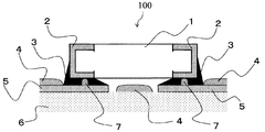
- FIG. 1 is a cross-sectional view illustrating a main part of the electronic control device 100 according to the first embodiment.
- the electrode 2 of the electronic component 1 and the conductor 5 (wiring) of the circuit board 6 are connected by the conductive bonding material 3.
- the electronic component 1 has, for example, a chip resistance 3216 size (3.2 mm ⁇ 1.6 mm), and the conductive bonding material 3 uses solder.
- the chip resistor shown in FIG. 1 is a leadless chip component.
- the circuit board 6 is a printed board, and includes a solder resist 4 and a conductor 5 for protecting wiring, and a non-metallic member 7 in a region (electrode pad) to which the solder of the conductor 5 is connected.
- the non-metallic member 7 is made of the same material as that of the solder resist 4, and in the electronic control device 100, the non-metallic member 7 exists between the electrode 2 of the electronic component 1 and the conductor 5 facing the solder.
- the electronic component 1 has an electrode 2, and the circuit board 6 has a conductor 5 that faces the electrode 2.
- the conductive bonding material 3 bonds the electrode 2 and the conductor 5 together.
- the nonmetallic member 7 (insulating member) is disposed in the conductive bonding material 3 and is in contact with the conductor 5 and the electrode 2. That is, the nonmetallic member 7 has a height in the direction connecting the electrode 2 and the conductor 5, and protrudes from the conductor 5 toward the electrode 2.
- the height from the surface of the conductor 5 (a 1st conductor and a 2nd conductor) of the two nonmetallic members 7 (a 1st insulating member and a 2nd insulating member) shown in FIG. 1 is the same. is there.
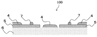
- FIG. 2 is a top view of the circuit board 6 before the electronic component 1 is mounted
- FIG. 3 is a cross-sectional view taken along the line X-X ′ of FIG.
- the nonmetallic member 7 is disposed on the conductor 5 to which the electronic component 1 is soldered.
- the non-metallic member 7 is the same material as the solder resist 4 applied as a protective film on the surface layer of the circuit board 6.
- the non-metallic member 7 (insulating member) is made of the same material as the solder resist 4 that protects the circuit board 6.
- the nonmetallic member 7 is separated from the solder resist 4 that protects the circuit board 6 and is isolated.
- the two non-metallic members 7 (the first insulating member and the second insulating member) are arranged in the arrangement direction of the two conductors 5 (the first conductor and the second conductor). Arranged in a row.
- the electronic control device 100 of this embodiment can be manufactured in the same process as the manufacturing process of the conventional printed circuit board and the electronic control device.
- the non-metallic member 7 that is a feature of the first embodiment is formed in an existing manufacturing process of “solder resist coating / exposure / development” in the printed circuit board manufacturing process.
- a solder resist is applied to the entire surface of the substrate by, for example, a spray method or a printing method (S10). Thereafter, in the “exposure” step, the portion where the solder resist is to be formed is cured by exposure using a photomask (S15). At this time, the solder resist is hardened in the soldering region of the conductor 5. In the next “development” step, the uncured portion that does not require the solder resist is washed away (S20).
- the non-metal member 7 formed as a result is a cylinder having a diameter of 0.1 mm, for example.
- the columnar non-metallic member 7 (insulating member) is formed on the conductor 5 of the circuit board 6 in the steps S10 to S20.
- a film-like solder resist 4 for protecting the circuit board 6 is also formed. That is, the columnar non-metallic member 7 is formed as a solder resist in the step of forming the solder resist 4 that protects the circuit board 6.
- the electronic component 1 is soldered to the circuit board 6 which is a manufacturing process of the electronic control device 100. This is the same as the conventional process, and a solder paste is printed on the conductor 5 of the substrate using a solder mask (S25). Thereafter, the electronic component 1 is mounted and the solder is cured in the reflow process (S30).
- the conductive bonding material 3 is disposed on the columnar non-metallic member 7 (insulating member) in the step S25, and the electronic component 1 is disposed on the conductive bonding material 3 in the step S30. Then, the electrode 2 of the electronic component 1 and the conductor 5 of the circuit board 6 are joined by the conductive joining material 3.
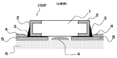
- FIG. 4 is a cross-sectional view showing an electronic control device 100P, which is a comparative example with the first embodiment.
- the electrode 2 of the electronic component 1 and the conductor 5 of the circuit board 6 are connected by the conductive bonding material 3, but the volume of the conductive bonding material 3 between the electronic component 1 and the conductor 5 is extremely small.
- the distance between the electrode 2 and the opposing conductor 5, that is, the connection height of the solder is about 10 ⁇ m, and in some cases, it may be substantially equal to zero. This is due to the weight of the electronic component 1, and the electronic component sinks into the molten solder during reflow, and the solder is cured as it is.
- FIG. 5 is a graph showing the relationship between the solder connection height and the solder thermal fatigue life.
- the solder connection height H affects the fatigue life Nf of the solder accompanying a change in temperature.
- the nonmetallic member 7 functions as a spacer when the electronic component 1 is mounted on the solder paste printed on the conductor 5 due to the presence of the nonmetallic member 7 disposed on the conductor 5 of the circuit board 6. Fulfill.
- the volume of the solder between the electronic component 1 and the conductor 5 is kept constant without the electronic component 1 sinking into the molten solder. That is, it is possible to keep the solder connection height higher than before and keep it constant.
- non-metallic member 7 is present in a form encased in solder, there is no fear of causing breakage starting from the non-metallic member such as peeling between the non-metallic member 7 and the conductor 5.
- the present embodiment provides an electronic control device with improved reliability without incurring a cost increase that can be realized only by existing processes.
- the graph of the relationship between the solder connection height H and the solder thermal fatigue life Nf shown in FIG. 5 also shows the relationship between the voids in the solder and the fatigue life. As can be seen from the graph, the fatigue life Nf of the solder decreases as the number of voids in the solder increases.
- the nonmetallic member 7 shown in FIGS. 1, 2, and 3 is a member having an electric resistance of 1 ⁇ 10 3 ⁇ or more. Due to the presence of the non-metallic member 7, voids in the solder can be reduced as will be described below.
- the non-metallic member 7 is made of a material having an electrical resistivity of 1 ⁇ 10 3 or more, thereby reducing voids in the solder after soldering and extending the fatigue life of the solder. Is possible. As a result, an electronic control device with improved reliability is realized.
- the height of the conductive bonding material 3 (solder) between the electrode 2 of the electronic component 1 and the conductor 5 of the circuit board 6 is secured by the non-metallic member 7, so that the fatigue life of the conductive bonding material 3 is maintained. Can be improved. Further, since the nonmetallic member 7 has insulating properties and lower wettability than the metal, an alloy layer is not formed at the boundary between the nonmetallic member 7 and the conductive bonding material 3, and convection occurs when the conductive bonding material 3 is melted. Is prone to occur. As a result, voids can be reduced.
- the non-metallic member 7 has a height in a direction connecting the electrode 2 of the electronic component 1 and the opposing conductor 5, and the height is 10 ⁇ m or more. In other words, the height of the nonmetallic member 7 (insulating member) from the surface of the conductor 5 is 10 ⁇ m or more.
- the non-metallic member 7 shown in FIGS. 1, 2, and 3 is a solder resist having a height of 30 ⁇ m. Moreover, it is set as a cylindrical shape with a diameter of 0.1 mm.
- the solder resist on the surface layer of the circuit board 6 generally has a thickness of 25 ⁇ m to 50 ⁇ m and a minimum coating width of 0.1 mm. Therefore, the nonmetallic member 7 can be formed only by the existing solder resist coating process in the manufacturing process of the circuit board 6.
- the thickness is smaller than the general thickness (100 to 150 ⁇ m) of the solder printing mask used in the solder printing process. Soldering can be performed in the same process as existing, without jumping out of the solder printing mask. As a result, an electronic control device with improved solder connection reliability can be obtained.
- the height of the conductive bonding material 3 for bonding the electrode 2 of the electronic component 1 and the conductor 5 of the circuit board 6 is secured, and the inside of the conductive bonding material 3 is secured. Voids can be reduced. As a result, the connection reliability of the conductive bonding material 3 is improved.
- the nonmetallic member 7 can be formed only by the existing solder resist coating process in the manufacturing process of the circuit board 6, the manufacturing cost can be reduced.
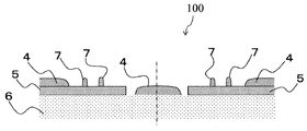
- FIG. 6 is a cross-sectional view showing a main part of the electronic control device 100 of the second embodiment.
- two nonmetallic members 7 are provided in the conductive bonding material 3 at a pair of bonding portions 8 and 9 between the electrode 2 of the electronic component 1 and the conductor 5 of the circuit board 6 facing each other.
- all the non-metallic members 7 are formed to have the same height.
- FIG. 7 is a top view of the circuit board 6, and FIG. 8 is a cross-sectional view taken along the line Y-Y 'of FIG.
- the joining portion 8 and the nonmetallic member 7 of the joining portion 9 are formed so as to be positioned symmetrically with respect to the center of the electronic component 1. That is, the nonmetallic member 7 (insulating member) is disposed symmetrically with respect to a plane that passes through the center of the electronic component 1 and is perpendicular to the arrangement direction of the electrodes 2 of the electronic component 1.
- all the non-metallic members 7 are arranged in the direction in which the two conductors 5 (first conductor and second conductor) are arranged. Arranged in a row.
- the non-metallic member 7 provided at each joint is symmetrical with respect to the center of the electronic component 1, when the electronic component 1 is mounted on the conductor 5 of the circuit board 6 and joined, The electronic component 1 is prevented from tilting. As a result, it is possible to obtain an electronic control device that increases the solder connection height without tilting the electronic component 1 and improves the solder connection reliability.
- thermosetting organic solvent is used for the non-metallic member 7 for example.
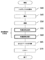
- S40 to S50 are the same as S10 to S20 of FIG. 10 except for the formation of the non-metallic member 7, and thus description thereof is omitted.
- thermosetting organic solvent is applied to the conductor 5 of the circuit board 6 in a columnar shape using, for example, a cylinder (S55).
- the non-metallic member 7 is formed by curing the organic solvent in an environment of the curing temperature of the organic solvent (S60).
- the conductive bonding material 3 of the circuit board 6 is applied by, for example, mask printing (S65).
- the electronic component 1 is mounted on the upper surface, and the electrode 2 of the electronic component 1, the conductive bonding material 3, and the conductor 5 are bonded by passing through the environment of the curing temperature of the conductive bonding material 3 (S ⁇ b> 70). ).
- the nonmetallic member 7 even when the nonmetallic member 7 is not formed in advance in the circuit board manufacturing process, it is possible to form the nonmetallic member 7 by adding a process before mounting the electronic component. As a result, it is possible to obtain an electronic control device that achieves a structure in which the solder connection height is increased and the voids in the solder are reduced, and the reliability is improved.
- the present invention is not limited to the above-described embodiment, and includes various modifications.
- the above-described embodiment has been described in detail for easy understanding of the present invention, and is not necessarily limited to the one having all the configurations described.
- a part of the configuration of an embodiment can be replaced with the configuration of another embodiment, and the configuration of another embodiment can be added to the configuration of an embodiment.
- the non-metallic member 7 (insulating member) is cylindrical, but may be prismatic. Moreover, the non-metallic member 7 may have a pillow shape (bank shape).
- the electronic component 1 may have two or more electrodes 2, and the circuit board 6 may have two or more conductors 5 respectively facing the electrodes 2.
- an electronic control device including a circuit board on which an electronic component is mounted, the electrode and the conductor are included in a conductive bonding material that joins an electrode of the electronic component and a conductor of the circuit board.
- An electronic control device in which a non-metallic member having a height in the direction of tying is disposed.
- the non-metallic member has a pair of electrodes facing each other along a planar direction of the circuit board, and the non-metallic member is formed of each conductive bonding material that joins the pair of electrodes and the conductor.
- the solder connection reliability is improved by controlling the solder connection height to be constant. And it can be realized only by existing processes.
- Patent Document 1 a solder paste for adjusting the solder connection height is used separately from the solder paste for connecting the electronic component and the electrode of the substrate.
- the solder paste for adjusting the solder height is partially applied on the solder resist on the board surface, and rises and collects on the land due to the surface tension of the solder melted at the time of reflow. Adjust. That is, the invention is an invention in which the solder connection height is controlled by the weight of the electronic component and the volume of the height adjusting solder paste.
- the scaffold of the electronic component mounted on the solder paste is an unstable molten solder at the time of reflow, and there is a concern that the electronic component is inclined and connected. Therefore, with the technology of Patent Document 1, it may be difficult to control the height to be constant without tilting the electronic component.
- Patent Document 2 relates to a structure for joining an electronic component to a substrate using solder balls.
- a metal core in the solder ball By providing a metal core in the solder ball, the solder connection height after reflowing is ensured to a certain level, and the solder connection reliability can be improved.
- Patent Document 2 requires a new manufacturing process for manufacturing a solder ball with a built-in metal core. The technique of Patent Document 2 is applied only to a structure using solder balls such as BGA (Ball Grid Array) or flip chip.
- BGA Ball Grid Array
Landscapes
- Engineering & Computer Science (AREA)
- Manufacturing & Machinery (AREA)
- Microelectronics & Electronic Packaging (AREA)
- Electric Connection Of Electric Components To Printed Circuits (AREA)
Abstract
L'invention concerne un procédé et un dispositif de circuit électronique qui permettent de réduire les manques dans un matériau de liaison conducteur qui lie une électrode d'un composant électronique et un conducteur d'une carte de circuit imprimé l'un à l'autre, tout en assurant la taille dudit matériau de liaison conducteur. Un dispositif de commande électronique (100) (dispositif de circuit électronique) est pourvu d'un composant électronique (1), d'une carte de circuit imprimé (6), d'un matériau de liaison conducteur (3) et d'un élément non métallique (7) (élément isolant). Le composant électronique (1) possède une électrode (2), et la carte de circuit imprimé (6) possède un conducteur (5) en regard de l'électrode (2). Le matériau de liaison conducteur (3) lie l'électrode (2) et le conducteur (5) l'un à l'autre. L'élément non métallique (7) (élément isolant) est disposé dans le matériau de liaison conducteur (3) et est en contact avec le conducteur (5) et l'électrode (2).
Priority Applications (1)
| Application Number | Priority Date | Filing Date | Title |
|---|---|---|---|
| JP2018519131A JPWO2017203859A1 (ja) | 2016-05-25 | 2017-04-11 | 電子回路装置及び方法 |
Applications Claiming Priority (2)
| Application Number | Priority Date | Filing Date | Title |
|---|---|---|---|
| JP2016-104213 | 2016-05-25 | ||
| JP2016104213 | 2016-05-25 |
Publications (1)
| Publication Number | Publication Date |
|---|---|
| WO2017203859A1 true WO2017203859A1 (fr) | 2017-11-30 |
Family
ID=60411732
Family Applications (1)
| Application Number | Title | Priority Date | Filing Date |
|---|---|---|---|
| PCT/JP2017/014757 Ceased WO2017203859A1 (fr) | 2016-05-25 | 2017-04-11 | Procédé et dispositif de circuit électronique |
Country Status (2)
| Country | Link |
|---|---|
| JP (1) | JPWO2017203859A1 (fr) |
| WO (1) | WO2017203859A1 (fr) |
Cited By (2)
| Publication number | Priority date | Publication date | Assignee | Title |
|---|---|---|---|---|
| JP2019186329A (ja) * | 2018-04-05 | 2019-10-24 | 新光電気工業株式会社 | 配線基板、電子装置 |
| JP2022028391A (ja) * | 2020-08-03 | 2022-02-16 | 三菱電機エンジニアリング株式会社 | プリント基板、プリント基板の製造方法および電子部品の実装方法 |
Citations (5)
| Publication number | Priority date | Publication date | Assignee | Title |
|---|---|---|---|---|
| JPH08181419A (ja) * | 1994-12-22 | 1996-07-12 | Nissan Motor Co Ltd | プリント配線板の構造 |
| JP2000332394A (ja) * | 1999-05-24 | 2000-11-30 | Taiyo Yuden Co Ltd | 電子部品実装用基板及びその製造方法 |
| JP2011258794A (ja) * | 2010-06-10 | 2011-12-22 | Denso Corp | 電子装置およびその製造方法 |
| JP2012124397A (ja) * | 2010-12-10 | 2012-06-28 | Cmk Corp | 部品内蔵型多層プリント配線板 |
| JP2012165156A (ja) * | 2011-02-07 | 2012-08-30 | Nippon Dempa Kogyo Co Ltd | 発振器 |
Family Cites Families (2)
| Publication number | Priority date | Publication date | Assignee | Title |
|---|---|---|---|---|
| JP2008226946A (ja) * | 2007-03-09 | 2008-09-25 | Nec Corp | 半導体装置およびその製造方法 |
| EP2293324B1 (fr) * | 2008-06-25 | 2019-05-15 | Panasonic Intellectual Property Management Co., Ltd. | Structure de conditionnement et procédé de fabrication de structure de conditionnement |
-
2017
- 2017-04-11 JP JP2018519131A patent/JPWO2017203859A1/ja active Pending
- 2017-04-11 WO PCT/JP2017/014757 patent/WO2017203859A1/fr not_active Ceased
Patent Citations (5)
| Publication number | Priority date | Publication date | Assignee | Title |
|---|---|---|---|---|
| JPH08181419A (ja) * | 1994-12-22 | 1996-07-12 | Nissan Motor Co Ltd | プリント配線板の構造 |
| JP2000332394A (ja) * | 1999-05-24 | 2000-11-30 | Taiyo Yuden Co Ltd | 電子部品実装用基板及びその製造方法 |
| JP2011258794A (ja) * | 2010-06-10 | 2011-12-22 | Denso Corp | 電子装置およびその製造方法 |
| JP2012124397A (ja) * | 2010-12-10 | 2012-06-28 | Cmk Corp | 部品内蔵型多層プリント配線板 |
| JP2012165156A (ja) * | 2011-02-07 | 2012-08-30 | Nippon Dempa Kogyo Co Ltd | 発振器 |
Cited By (3)
| Publication number | Priority date | Publication date | Assignee | Title |
|---|---|---|---|---|
| JP2019186329A (ja) * | 2018-04-05 | 2019-10-24 | 新光電気工業株式会社 | 配線基板、電子装置 |
| JP7015721B2 (ja) | 2018-04-05 | 2022-02-03 | 新光電気工業株式会社 | 配線基板、電子装置 |
| JP2022028391A (ja) * | 2020-08-03 | 2022-02-16 | 三菱電機エンジニアリング株式会社 | プリント基板、プリント基板の製造方法および電子部品の実装方法 |
Also Published As
| Publication number | Publication date |
|---|---|
| JPWO2017203859A1 (ja) | 2019-02-14 |
Similar Documents
| Publication | Publication Date | Title |
|---|---|---|
| KR100921919B1 (ko) | 반도체 칩에 형성되는 구리기둥-주석범프 및 그의 형성방법 | |
| JP6206494B2 (ja) | 半導体装置 | |
| CN101145545A (zh) | 包括元件安装表面被树脂层涂覆的布线基板的半导体装置 | |
| KR101054440B1 (ko) | 전자 소자 패키지 및 그 제조 방법 | |
| JP2004266074A (ja) | 配線基板 | |
| US7928559B2 (en) | Semiconductor device, electronic component module, and method for manufacturing semiconductor device | |
| US20250183125A1 (en) | Electronic device and method for manufacturing electronic device | |
| JP2019140179A (ja) | フリップチップ実装用の基板およびこれを用いた電子装置 | |
| JP2009105209A (ja) | 電子装置及びその製造方法 | |
| US20150144390A1 (en) | Wiring board and method for mounting semiconductor element on wiring board | |
| KR101101550B1 (ko) | 솔더 볼 및 반도체 패키지 | |
| WO2017203859A1 (fr) | Procédé et dispositif de circuit électronique | |
| US20100127382A1 (en) | Semiconductor device | |
| JP2010272563A (ja) | 部品内蔵配線板、部品内蔵配線板の製造方法 | |
| JP4952365B2 (ja) | 両面実装回路基板に対する電子部品の実装構造、半導体装置、及び両面実装半導体装置の製造方法 | |
| JP2004128290A (ja) | 半導体装置 | |
| JP5062376B1 (ja) | 電子部品実装基板の製造方法 | |
| JP4267549B2 (ja) | 半導体装置およびその製造方法ならびに電子機器 | |
| JP5369875B2 (ja) | 部品内蔵配線板、部品内蔵配線板の製造方法 | |
| JP2013211497A (ja) | 部品接合構造 | |
| JP2016162813A (ja) | プリント基板及びハンダ付け方法 | |
| JP5601413B2 (ja) | 部品内蔵配線板、部品内蔵配線板の製造方法 | |
| JP5577734B2 (ja) | 電子装置および電子装置の製造方法 | |
| JP2001168224A (ja) | 半導体装置、電子回路装置および製造方法 | |
| US20230005830A1 (en) | Semiconductor apparatus |
Legal Events
| Date | Code | Title | Description |
|---|---|---|---|
| ENP | Entry into the national phase |
Ref document number: 2018519131 Country of ref document: JP Kind code of ref document: A |
|
| NENP | Non-entry into the national phase |
Ref country code: DE |
|
| 121 | Ep: the epo has been informed by wipo that ep was designated in this application |
Ref document number: 17802459 Country of ref document: EP Kind code of ref document: A1 |
|
| 122 | Ep: pct application non-entry in european phase |
Ref document number: 17802459 Country of ref document: EP Kind code of ref document: A1 |