WO2017204151A1 - 磁気センサ - Google Patents
磁気センサ Download PDFInfo
- Publication number
- WO2017204151A1 WO2017204151A1 PCT/JP2017/019009 JP2017019009W WO2017204151A1 WO 2017204151 A1 WO2017204151 A1 WO 2017204151A1 JP 2017019009 W JP2017019009 W JP 2017019009W WO 2017204151 A1 WO2017204151 A1 WO 2017204151A1
- Authority
- WO
- WIPO (PCT)
- Prior art keywords
- magnetic
- convergence
- region
- magnetic sensor
- magnetosensitive
- Prior art date
- Legal status (The legal status is an assumption and is not a legal conclusion. Google has not performed a legal analysis and makes no representation as to the accuracy of the status listed.)
- Ceased
Links
Images


Classifications
-
- G—PHYSICS
- G01—MEASURING; TESTING
- G01R—MEASURING ELECTRIC VARIABLES; MEASURING MAGNETIC VARIABLES
- G01R33/00—Arrangements or instruments for measuring magnetic variables
- G01R33/0011—Arrangements or instruments for measuring magnetic variables comprising means, e.g. flux concentrators, flux guides, for guiding or concentrating the magnetic flux, e.g. to the magnetic sensor
-
- G—PHYSICS
- G01—MEASURING; TESTING
- G01R—MEASURING ELECTRIC VARIABLES; MEASURING MAGNETIC VARIABLES
- G01R33/00—Arrangements or instruments for measuring magnetic variables
- G01R33/02—Measuring direction or magnitude of magnetic fields or magnetic flux
- G01R33/06—Measuring direction or magnitude of magnetic fields or magnetic flux using galvano-magnetic devices
- G01R33/09—Magnetoresistive devices
- G01R33/093—Magnetoresistive devices using multilayer structures, e.g. giant magnetoresistance sensors
-
- G—PHYSICS
- G01—MEASURING; TESTING
- G01R—MEASURING ELECTRIC VARIABLES; MEASURING MAGNETIC VARIABLES
- G01R33/00—Arrangements or instruments for measuring magnetic variables
- G01R33/02—Measuring direction or magnitude of magnetic fields or magnetic flux
-
- G—PHYSICS
- G01—MEASURING; TESTING
- G01R—MEASURING ELECTRIC VARIABLES; MEASURING MAGNETIC VARIABLES
- G01R33/00—Arrangements or instruments for measuring magnetic variables
- G01R33/02—Measuring direction or magnitude of magnetic fields or magnetic flux
- G01R33/06—Measuring direction or magnitude of magnetic fields or magnetic flux using galvano-magnetic devices
- G01R33/09—Magnetoresistive devices
-
- G—PHYSICS
- G01—MEASURING; TESTING
- G01R—MEASURING ELECTRIC VARIABLES; MEASURING MAGNETIC VARIABLES
- G01R33/00—Arrangements or instruments for measuring magnetic variables
- G01R33/0047—Housings or packaging of magnetic sensors ; Holders
-
- H—ELECTRICITY
- H10—SEMICONDUCTOR DEVICES; ELECTRIC SOLID-STATE DEVICES NOT OTHERWISE PROVIDED FOR
- H10N—ELECTRIC SOLID-STATE DEVICES NOT OTHERWISE PROVIDED FOR
- H10N50/00—Galvanomagnetic devices
- H10N50/10—Magnetoresistive devices
Definitions
- the present invention relates to a magnetic sensor, and more particularly to a magnetic sensor in which four magnetosensitive elements are bridge-connected.
- Magnetic sensors using magnetosensitive elements are widely used in ammeters and magnetic encoders.
- the magnetic sensor may be provided with an external magnetic body for collecting magnetic flux in the magnetosensitive element.
- it is difficult to increase the detection accuracy because the magnetic flux to be detected is not sufficiently concentrated on the magnetosensitive element.
- the magnetic sensor described in Patent Document 2 is provided with a magnetic layer on a sensor substrate on which a magnetosensitive element is formed, thereby concentrating the magnetic flux to be detected on the magnetosensitive element.
- a magnetic sensor described in Patent Document 2 two gaps are formed using three magnetic layers, and two magnetosensitive elements are arranged in each of the two gaps, so that a total of four magnetosensitive elements are provided. Constitutes a bridge circuit.
- an object of the present invention is to provide an improved magnetic sensor in which four magnetosensitive elements are bridge-connected.
- a magnetic sensor includes a sensor substrate, first, second, and third magnetic layers provided on the sensor substrate, and first, second, third, and fourth magnetosensitive elements that are bridge-connected.
- the first magnetic layer includes: a first main region; and first, second, third, and fourth convergence regions that decrease in width as they move away from the first main region.
- the second magnetic layer includes a second main region, and fifth and seventh convergence regions whose width decreases as the distance from the second main region increases.
- the layer includes a third main region, and sixth and eighth convergence regions that become narrower as the distance from the third main region decreases, and the first, second, third, and fourth convergence regions And the ends of the fifth, sixth, seventh and eighth convergence regions are respectively connected to the first, second, third and fourth gaps.
- the first, second, third and fourth magnetosensitive elements are arranged on magnetic paths formed by the first, second, third and fourth gaps, respectively. To do.
- the magnetic flux generated by the current flowing through each magnetosensitive element affects the other magnetosensitive elements. There is no. This makes it possible to provide a magnetic sensor with higher detection accuracy.
- the magnetic sensor according to the present invention preferably further includes a first external magnetic body provided on the sensor substrate so as to cover the first main region. According to this, the selectivity of the magnetic flux perpendicular to the sensor substrate can be enhanced.
- the width of the first external magnetic body in the first direction which is the extending direction of the first to fourth gaps, is wider than the width of the first main region in the first direction.
- the magnetic sensor according to the present invention further includes a second external magnetic body provided in the vicinity of the second main region and a third external magnetic body provided in the vicinity of the third main region. Is preferred. According to this, higher detection accuracy can be obtained.
- the first convergence area and the fourth convergence area are lines having a first straight line extending in a first direction which is an extending direction of the first to fourth gaps as an axis of symmetry. It is preferable that the second convergence region and the third convergence region are symmetrical with respect to the first straight line as an axis of symmetry. According to this, since the balance of the magnetic flux applied to the 1st and 4th magnetosensitive elements and the balance of the magnetic flux applied to the 2nd and 3rd magnetosensitive elements are raised, higher detection accuracy is achieved. Can be obtained.
- the first convergence region and the third convergence region may have a second straight line extending in a second direction orthogonal to the extending direction of the first to fourth gaps as a symmetry axis.
- the second convergence region and the fourth convergence region are line symmetric with respect to the second straight line as an axis of symmetry
- the fifth convergence region and the seventh convergence region are It is preferable that the second straight line is symmetric with respect to the axis of symmetry
- the sixth convergence area and the eighth convergence area are line symmetric with respect to the second straight line as the axis of symmetry.
- the first and third magnetosensitive elements overlap with the first and second magnetic layers
- the second and fourth magnetosensitive elements are the first and second magnetosensitive elements. It may overlap with the third magnetic layer. According to this, since the leakage magnetic flux is reduced, higher detection accuracy can be obtained.
- the first magnetic layer is preferably provided with a notch having a loop-shaped outer periphery. According to this, since the residual magnetic flux of the first magnetic layer circulates around the outer periphery of the notch portion, it is possible to prevent a decrease in detection accuracy due to the residual magnetic flux.
- the first, second, third and fourth magnetosensitive elements each have a plurality of sensitive elements arranged on a magnetic path formed by the first, second, third and fourth gaps. Magnetic elements may be connected in series. According to this, higher detection accuracy can be obtained.
- the magnetic sensor according to the present invention includes a fourth magnetic body disposed between the plurality of magnetic sensing elements that respectively constitute the first, second, third, and fourth magnetic sensing elements in a plan view. It is preferable to further comprise a layer. According to this, it becomes possible to reduce the magnetic flux leakage between the plurality of magnetosensitive elements. Furthermore, in this case, the fourth magnetic layer may have an overlap with the plurality of magnetosensitive elements respectively constituting the first, second, third and fourth magnetosensitive elements. According to this, it becomes possible to further reduce the leakage magnetic flux between the plurality of magnetosensitive elements.
- the fourth magnetic layer may be divided in a first direction that is an extending direction of the first to fourth gaps. According to this, since the fourth magnetic layer has magnetic anisotropy, higher detection accuracy can be obtained.
- each of the first to fourth magnetosensitive elements is a magnetoresistive element.
- the sensitivity directions of the magnetoresistive elements constituting the first to fourth magnetosensitive elements are the same, and the magnetoresistive elements constituting the first to fourth magnetosensitive elements are spins.
- a valve type GMR element is preferred.
- the four magnetosensitive elements are arranged on magnetic paths formed by different gaps, a magnetic sensor with high detection accuracy is configured by bridge-connecting these four magnetosensitive elements. It becomes possible.
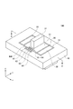
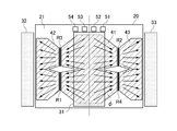
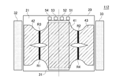
- FIG. 1 is a schematic perspective view showing an appearance of a magnetic sensor 100 according to a preferred embodiment of the present invention.
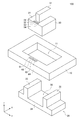
- FIG. 2 is a schematic exploded perspective view of the magnetic sensor 100.
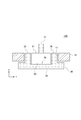
- FIG. 3 is a schematic cross-sectional view along the line AA shown in FIG.
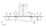
- FIG. 4 is a schematic plan view for explaining the structure of the element formation surface 21 of the sensor substrate 20.
- FIG. 5 is a schematic cross-sectional view along the line BB shown in FIG. It is a figure for demonstrating a mode that magnetic flux (phi) is equally distributed.
- FIG. 7 is a circuit diagram for explaining the connection relationship between the magnetosensitive elements R1 to R4 and the bonding pads 51 to 54. In FIG. FIG. FIG.
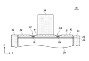
- FIG. 8 is a schematic cross-sectional view for explaining the configuration of the main part of the magnetic sensor 101 according to the first modification.
- FIG. 9 is a schematic cross-sectional view for explaining the configuration of the main part of the magnetic sensor 102 according to the second modification.
- FIG. 10 is a schematic cross-sectional view for explaining the configuration of the main part of the magnetic sensor 103 according to the third modification.
- FIG. 11 is a schematic cross-sectional view for explaining the configuration of the main part of the magnetic sensor 104 according to the fourth modification.
- FIG. 12 is a schematic cross-sectional view for explaining the configuration of the main part of the magnetic sensor 105 according to the fifth modification.
- FIG. 13 is a schematic cross-sectional view for explaining the configuration of the main part of the magnetic sensor 106 according to the sixth modification.
- FIG. 14 is a schematic plan view for explaining the configuration of the main part of the magnetic sensor 107 according to the seventh modification.
- FIG. 15 is a schematic plan view for explaining the configuration of the main part of the magnetic sensor 108 according to the eighth modification.
- FIG. 16 is a schematic plan view for explaining the configuration of the main part of the magnetic sensor 109 according to the ninth modification.
- FIG. 17 is a schematic plan view for explaining the configuration of the main part of the magnetic sensor 110 according to the tenth modification.
- FIG. 18 is a schematic plan view for explaining the configuration of the main part of the magnetic sensor 111 according to the eleventh modification.
- FIG. 19 is a schematic plan view for explaining the configuration of the main part of the magnetic sensor 112 according to the twelfth modification.
- FIG. 20 is a schematic plan view for explaining the configuration of the main part of the magnetic sensor 108 according to the eighth modification.
- FIG. 21 is a schematic cross-sectional view for explaining the configuration of the main part of the magnetic sensor 114 according to the fourteenth modification.
- FIG. 22 is a schematic plan view for explaining the configuration of the main part of the magnetic sensor 115 according to the fifteenth modification.
- FIG. 23 is a schematic cross-sectional view for explaining the configuration of the main part of the magnetic sensor 116 according to the sixteenth modification.
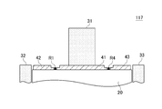
- FIG. 24 is a schematic cross-sectional view for explaining the configuration of the main part of a magnetic sensor 117 according to the seventeenth modification.
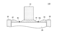
- FIG. 25 is a schematic cross-sectional view for explaining the configuration of the main part of a magnetic sensor 118 according to an eighteenth modification.
- FIG. 26 is a schematic perspective view for explaining the configuration of the main part of a magnetic sensor 119 according to a nineteenth modification.
- FIG. 1 is a schematic perspective view showing an appearance of a magnetic sensor 100 according to a preferred embodiment of the present invention.
- 2 is a schematic exploded perspective view of the magnetic sensor 100
- FIG. 3 is a schematic cross-sectional view taken along the line AA shown in FIG.
- the magnetic sensor 100 includes a circuit board 10 having an opening 11, a sensor board 20 disposed in the opening 11, and a first fixed to the sensor board 20.
- the sensor substrate 20 is a chip component that is smaller than the circuit substrate 10 and has a magnetosensitive element to be described later.
- the first to fourth external magnetic bodies 31 to 34 are blocks made of a soft magnetic material having high magnetic permeability such as ferrite.
- the sensor substrate 20 has a substantially rectangular parallelepiped shape, and a first external magnetic body 31 is disposed on the element forming surface 21 constituting the xy plane.
- a method for producing the sensor substrate 20 a method is generally used in which a large number of sensor substrates 20 are simultaneously formed on a collective substrate, and a large number are separated by separating them, but the present invention is not limited thereto.
- the individual sensor substrates 20 may be manufactured separately.
- four magnetosensitive elements R1 to R4 and three magnetic layers 41 to 43 are formed on the element forming surface 21.
- four bonding pads 51 to 54 are provided on the element forming surface 21 and are connected to bonding pads 61 to 64 provided on the circuit board 10 through corresponding bonding wires BW, respectively.
- the second and third external magnetic bodies 32 and 33 are respectively disposed on both sides of the sensor substrate 20 in the x direction.
- the second and third external magnetic bodies 32 and 33 are connected via a fourth external magnetic body 34 located at the bottom of the sensor substrate 20, whereby the second to fourth external magnetic bodies 32 to 32 are connected.
- 34 constitutes a single magnetic block 35.
- the magnetic block 35 is disposed so as to be inserted into the opening 11 of the circuit board 10.
- the magnetic block 35 is provided with a concave portion 36 for accommodating the sensor substrate 20. When the sensor substrate 20 is accommodated in the concave portion 36, the element forming surface 21 of the sensor substrate 20 and the second and third elements are formed.
- the tips of the external magnetic bodies 32 and 33 are close to each other and form substantially the same plane.
- FIG. 4 is a schematic plan view for explaining the structure of the element formation surface 21 of the sensor substrate 20.
- FIG. 5 is a schematic cross-sectional view along the line BB shown in FIG.
- first to third magnetic layers 41 to 43 are formed on the element formation surface 21 of the sensor substrate 20.
- the first magnetic layer 41 is located approximately at the center of the element formation surface 21, and the second and third magnetic layers 42 and 43 are disposed on both sides in the x direction.
- the magnetic layers 41 to 43 may be a film made of a composite magnetic material in which a magnetic filler is dispersed in a resin material, or made of a soft magnetic material such as nickel or permalloy. It may be a thin film or foil, or may be a thin film or bulk sheet made of ferrite or the like.
- the first magnetic layer 41 includes a first main region M1 located in the center and first to fourth convergence regions S1 to S4 whose width in the y direction becomes narrower as they move away from the first main region M1 in the x direction. Includes S4.
- the first main region M ⁇ b> 1 is a part covered with the first external magnetic body 31.
- the width of the first external magnetic body 31 in the y direction is wider than the width of the first main region M1 in the y direction, and thereby the y direction of the first main region M1.
- a rotational shift can be considered.
- the first to fourth convergence regions S1 to S4 are tapered portions whose width in the y direction becomes narrower as they move away from the first main region M1 in the x direction.
- the third convergence regions S1, S3 are positioned on the negative side (left side) in the x direction with respect to the first main region M1, and the second and fourth convergence regions S2, S4 are relative to the first main region M1. Located on the x direction plus side (right side).
- the first magnetic layer 41 has a two-fold symmetrical shape.
- the first convergence region S1 and the fourth convergence region S4 are axisymmetric with respect to the virtual straight line L1 extending in the y direction, and the second convergence region S2 and the third convergence region S4
- the convergence region S3 is line symmetric.
- the first convergence region S1 and the third convergence region S3 are axisymmetric with respect to a virtual straight line L2 extending in the x direction, and the second convergence region S4 and the fourth convergence region.
- the region S4 is line symmetric. Due to such a symmetrical shape, when the magnetic flux taken in via the first external magnetic body 31 is incident on the first main region M1, the magnetic flux ⁇ is changed from the first to the first as shown in FIG.
- the four convergence regions S1 to S4 are distributed almost evenly.
- the distributed magnetic flux ⁇ passes through the first to fourth converging regions S1 to S4 having a tapered shape, so that the magnetic flux density is increased.
- the second magnetic layer 42 includes a second main region M2, and fifth and seventh convergence regions whose width in the y direction becomes narrower as they move away from the second main region M2 in the x direction (plus side). Includes S5 and S7.
- the third magnetic layer 43 has a third main region M3 and sixth and eighth convergences whose width in the y direction becomes narrower as they move away from the third main region M3 in the x direction (minus side). Regions S6 and S8 are included.
- the second main region M2 is located in the vicinity of the end of the sensor substrate 20 on the minus side in the x direction, and thereby approaches the second external magnetic body 32.
- the third main region M3 is located in the vicinity of the end of the sensor substrate 20 on the positive side in the x direction, and thereby close to the third external magnetic body 33.
- the front end portion of the fifth convergence region S5 is opposed to the front end portion of the first convergence region S1 via the first gap G1.
- the tip of the seventh convergence region S7 is opposed to the tip of the third convergence region S3 via the third gap G3.
- the fifth convergence region S5 and the seventh convergence region S7 are line symmetric with respect to a virtual straight line L2 extending in the x direction. Due to such a symmetrical shape, when the magnetic flux taken in via the second external magnetic body 32 is incident on the second main region M2, this magnetic flux enters the fifth and seventh convergence regions S5 and S7. It is distributed almost evenly.
- the tip of the sixth convergence region S6 is opposed to the tip of the second convergence region S2 via the second gap G2.
- the tip of the eighth convergence region S8 is opposed to the tip of the fourth convergence region S4 via the fourth gap G4.
- the sixth convergence region S6 and the eighth convergence region S8 are line symmetric with respect to a virtual straight line L2 extending in the x direction. Due to such a symmetrical shape, when the magnetic flux taken in via the third external magnetic body 33 enters the third main region M3, this magnetic flux enters the sixth and eighth convergence regions S6 and S8. It is distributed almost evenly.
- first to fourth magnetosensitive elements R1 to R4 extending in the y direction are arranged in the first to fourth gaps G1 to G4, respectively.
- the widths of the first to fourth gaps G1 to G4 in the x direction are the same.
- the first to fourth magnetosensitive elements R1 to R4 are not in contact with the first to third magnetic layers 41 to 43.
- the magnetosensitive elements R1 to R4 are not particularly limited as long as their physical characteristics change depending on the magnetic flux density, but are preferably magnetoresistive elements whose electrical resistance changes according to the direction of the magnetic field, and are spin valve GMR elements. It is particularly preferred that In the present embodiment, the sensitivity directions (fixed magnetization directions) of the magnetosensitive elements R1 to R4 are all aligned in the direction indicated by the arrow C in FIGS. 4 and 5 (plus side in the x direction).
- the first external magnetic body 31 plays a role of collecting the magnetic flux ⁇ in the z direction and releasing it to the first main region M ⁇ b> 1 of the first magnetic layer 41.
- the height of the first external magnetic body 31 in the z direction is not particularly limited, but the selectivity of the magnetic flux in the z direction can be increased by increasing the height in the z direction. However, if the height of the first external magnetic body 31 in the z direction is too high, the support of the first external magnetic body 31 may become unstable. It is preferable to do.
- the magnetic flux ⁇ collected in the first main region M1 via the first external magnetic body 31 is distributed substantially evenly to the first to fourth convergence regions S1 to S4. After that, they are emitted to the fifth to eighth convergence regions S5 to S8 through the first to fourth magnetosensitive elements R1 to R4, respectively.
- magnetic fluxes in opposite directions are applied to the magnetic sensitive elements R1, R3 and the magnetic sensitive elements R2, R4.
- the magnetization fixed directions of the magnetosensitive elements R1 to R4 are oriented in the x plus direction indicated by the arrow C, the magnetic sensitive elements R1 to R4 are sensitive to the component in the x direction of the magnetic flux.
- the magnetic flux that has reached the fifth and seventh convergence regions S5 and S7 is collected by the second external magnetic body 32 via the second main region M2.
- the magnetic flux that has reached the sixth and eighth convergence regions S6 and S8 is recovered by the third external magnetic body 33 via the third main region M3.
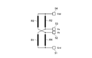
- FIG. 7 is a circuit diagram for explaining the connection relationship between the magnetosensitive elements R1 to R4 and the bonding pads 51 to 54.
- the bonding pads 51 and 54 are supplied with the ground potential Gnd and the power supply potential Vdd from the circuit board 10 side, respectively. Further, between the bonding pads 51 and 54, the magnetosensitive elements R1 and R2 are connected in series, and the magnetosensitive elements R4 and R3 are connected in series. The connection points of the magnetic sensitive elements R3 and R4 are connected to the bonding pad 52, and the connection points of the magnetic sensitive elements R1 and R2 are connected to the bonding pad 53.
- the connection points of the magnetic sensitive elements R1 and R2 are connected to the bonding pad 53.
- This difference is doubled by the differential bridge circuit shown in FIG. 7 and appears on the bonding pads 52 and 53.
- the circuit board 10 is provided with a voltage detection circuit (not shown), and the magnetic flux density can be measured by detecting the difference between the potentials Va and Vb appearing at the bonding pads 52 and 53.
- the first to third magnetic layers 41 to 43 are provided on the element forming surface 21 of the sensor substrate 20, and 4 formed by these magnetic layers 41 to 43. Since the magnetic sensing elements R1 to R4 are respectively disposed in the two gaps G1 to G4, the magnetic flux generated by the current flowing through one magnetic sensing element does not affect the other magnetic sensing elements. This makes it possible to obtain higher detection accuracy than before.
- the eight converging regions S1 to S8 constituting the gaps G1 to G4 all have a tapered shape whose width becomes narrower toward the corresponding magnetosensitive elements R1 to R4.
- the density of magnetic flux applied to R4 is increased.
- the first main region M1 included in the first magnetic layer 41 has a wide area connected to all the root portions of the four convergence regions S1 to S4, the first external region The magnetic flux collecting effect of the magnetic flux ⁇ via the magnetic body 31 is high, which makes it possible to obtain high detection accuracy.
- the magnetic sensor 100 according to the present embodiment includes the first external magnetic body 31, it can selectively detect the magnetic flux in the z direction. Moreover, since the second external magnetic body 32 and the third external magnetic body 33 are integrated in the magnetic sensor 100 according to the present embodiment, the magnetic resistance of the magnetic flux that circulates behind the sensor substrate 20 is reduced. You can also.
- FIG. 8 is a schematic cross-sectional view for explaining the configuration of the main part of the magnetic sensor 101 according to the first modification.
- insulating layers 22 and 23 are laminated in this order on the surface of the sensor substrate 20, and the surface of the insulating layer 22 constitutes the element forming surface 21.
- Magnetosensitive elements R1 to R4 are provided on the surface of the insulating layer 22, which is the element forming surface 21, and magnetic layers 41 to 43 are provided on the surface of the insulating layer 23 located on the upper layer.
- the magnetosensitive elements R1 to R4 and the magnetic layers 41 to 43 are located in different layers, and the gap G1 formed by the magnetic layers 41 and 42 ( G3) is disposed at a position overlapping with G3) in plan view, and the magnetosensitive element R4 (R2) is disposed at a position overlapping with gap G4 (G2) formed by the magnetic layers 41 and 43 in plan view. Be placed.
- the positions of the magnetosensitive elements R1 to R4 and the magnetic layers 41 to 43 in the z direction may be different from each other.
- the magnetic sensing elements R1 to R4 are not strictly located between the gaps G1 to G4, but are arranged on the magnetic path formed by the gaps G1 to G4, the magnetic flux passing through the gaps G1 to G4. Can be detected correctly.
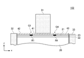
- FIG. 9 is a schematic cross-sectional view for explaining the configuration of the main part of the magnetic sensor 102 according to the second modification.
- a part of the magnetosensitive element R1 (R3) overlaps with the magnetic layers 41 and 42 in the z direction
- a part of the magnetosensitive element R4 is the magnetic layer 41. 43 in the z direction.
- the magnetic sensitive elements R1 to R4 are not strictly located between the gaps G1 to G4, they are arranged on the magnetic path formed by the gaps G1 to G4.
- FIG. 10 is a schematic cross-sectional view for explaining the configuration of the main part of the magnetic sensor 103 according to the third modification.
- insulating layers 24, 25, and 26 are laminated in this order on the surface of the sensor substrate 20, and the surface of the insulating layer 25 constitutes the element formation surface 21.
- Magnetic sensing elements R1 to R4 are provided on the surface of the insulating layer 25, which is the element formation surface 21, and magnetic layers 42 and 43 are provided on the surface of the insulating layer 24 located in the lower layer, and the insulating layer located in the upper layer. 26 is provided with a magnetic layer 41.
- the magnetic layer 41 and the magnetic layers 42 and 43 are located in different layers, and the three-dimensional gaps G1 to G4 are formed by overlapping these parts. Is formed.
- the magnetic sensing elements R1 to R4 are arranged between the gaps G1 to G4. As illustrated by the magnetic sensor 103 according to the third modification, the gaps G1 to G4 do not have to be planar, and may be three-dimensional.
- FIG. 11 is a schematic cross-sectional view for explaining the configuration of the main part of the magnetic sensor 104 according to the fourth modification.
- the magnetic layer 41 and the magnetic layers 42 and 43 are located in different layers and do not overlap each other. Therefore, oblique gaps G1 to G4 are formed by the magnetic layer 41 and the magnetic layers 42 and 43, and the magnetosensitive elements R1 to R4 are arranged at positions corresponding to the gaps G1 to G4. In this case, the magnetosensitive elements R1 to R4 and the magnetic layers 41 to 43 may or may not overlap.
- FIG. 12 is a schematic cross-sectional view for explaining the configuration of the main part of the magnetic sensor 105 according to the fifth modification.
- the second external magnetic body 32 and the third external magnetic body 33 are not integrated and are separated from each other.
- the magnetic resistance of the magnetic flux that circulates behind the sensor substrate 20 slightly increases, the same effect as that of the magnetic sensor 100 described above can be obtained.
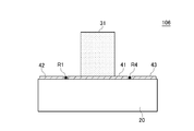
- FIG. 13 is a schematic cross-sectional view for explaining the configuration of the main part of the magnetic sensor 106 according to the sixth modification.
- the second and third external magnetic bodies 32 and 33 are omitted.
- the magnetic collection effect by the second and third external magnetic bodies 32 and 33 is eliminated, substantially the same effect as the magnetic sensor 100 described above can be obtained.
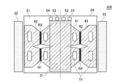
- FIG. 14 is a schematic plan view for explaining the configuration of the main part of the magnetic sensor 107 according to the seventh modification.
- the magnetic layers 41 to 43 are provided with slits, and each of the magnetic layers 41 to 43 is divided into a plurality of pieces by the slits.
- the magnetic layer 41 is provided with a cross-shaped slit, whereby the first to fourth convergence regions S1 to S4 are separated from each other.
- the magnetic layers 42 and 43 are provided with slits extending in the x direction, whereby the fifth and seventh convergence regions S5 and S7 are separated from each other, and the sixth and eighth convergence regions S6. , S8 are separated from each other.
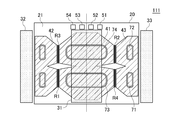
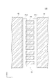
- FIG. 15 is a schematic plan view for explaining the configuration of the main part of the magnetic sensor 108 according to the eighth modification.
- the notch portion 71 is an independent space pattern having a loop-shaped outer periphery, and each of the cutout portions 71 is an ellipse having a major axis direction in the y direction.
- An independent space pattern means that the outer periphery is closed.
- four notches 71 are provided in the first magnetic layer 41, and two notches 71 are provided in the second and third magnetic layers 42 and 43, respectively. .
- a notch 71 is arranged avoiding the first main region M1, thereby preventing a reduction in the magnetic flux collecting effect in the first main region M1. If such a notch 71 is provided, the residual magnetic flux of the first to third magnetic layers 41 to 43 circulates around the outer periphery of the notch 71, thereby preventing a decrease in detection accuracy due to the residual magnetic flux. It becomes possible.
- FIG. 16 is a schematic plan view for explaining the configuration of the main part of the magnetic sensor 109 according to the ninth modification.
- the example shown in FIG. 16 is different from the example shown in FIG. 15 in that island-like independent patterns 72 are provided in the inner diameter region of the notch 71.
- the independent pattern 72 is separated from the first to third magnetic layers 41 to 43 through the notch 71. If such an independent pattern 72 is added, an increase in magnetic resistance due to the formation of the notch 71 can be minimized.
- FIG. 17 is a schematic plan view for explaining the configuration of the main part of the magnetic sensor 110 according to the tenth modification.
- the example shown in FIG. 17 is different from the example shown in FIG. 15 in that two notches 73 are provided in the first magnetic layer 41.
- the notch 73 is also an independent space pattern having a loop-shaped outer periphery, and all of them are elliptical with the x direction as the major axis direction. Even with such a configuration, the same effect as the example shown in FIG. 15 can be obtained.
- FIG. 18 is a schematic plan view for explaining the configuration of the main part of the magnetic sensor 111 according to the eleventh modification.
- the example shown in FIG. 18 is different from the example shown in FIG. 17 in that island-like independent patterns 74 are provided in the inner diameter region of the notch 73.
- the independent pattern 74 is separated from the first magnetic layer 41 through the notch 73. If such an independent pattern 74 is added, an increase in magnetic resistance due to the formation of the notch 73 can be minimized.
- FIG. 19 is a schematic plan view for explaining the configuration of the main part of the magnetic sensor 112 according to the twelfth modification.
- the edges of the first to eighth convergence regions S1 to S8 are curvilinear. With such a configuration, the flow of magnetic flux in the first to eighth convergence regions S1 to S8 becomes smoother and the magnetic resistance decreases.
- FIG. 20 is a schematic plan view for explaining the configuration of the main part of the magnetic sensor 113 according to the thirteenth modification.
- the first to fourth magnetosensitive elements R1 to R4 are constituted by two magnetosensitive elements arranged in the first to fourth gaps G1 to G4, respectively.
- the first magnetosensitive element R1 is configured by the two magnetosensitive elements R11 and R12 connected in series
- the second magnetosensitive element R2 is configured by the two magnetosensitive elements R21 and R22 connected in series
- the third magnetosensitive element R3 is configured by the two magnetosensitive elements R31 and R32 configured and connected in series
- the fourth magnetosensitive element R4 is configured by the two magnetosensitive elements R41 and R42 connected in series. ing.
- a fourth magnetic layer 44 may be added between two magnetosensitive elements (for example, R11 and R12) connected in series. Further, each of the magnetosensitive elements R1 to R4 may be constituted by three or more magnetosensitive elements connected in series.
- FIG. 21 is a schematic cross-sectional view for explaining the configuration of the main part of the magnetic sensor 114 according to the fourteenth modification.
- the magnetosensitive element R1 includes two magnetosensitive elements R11 and R12, and a part of the magnetosensitive element R11 overlaps the magnetic layers 41 and 44. The portion overlaps the magnetic layers 42 and 44.
- the other magnetosensitive elements R2 to R4 (not shown) have the same configuration. As described above, when the fourth magnetic layer 44 is provided and the magnetic sensitive elements R1 to R4 and the magnetic layers 41 to 44 are arranged so as to overlap with each other, the leakage magnetic flux is reduced, so that higher detection accuracy is obtained. It becomes possible.
- FIG. 22 is a schematic plan view for explaining the configuration of the main part of the magnetic sensor 115 according to the fifteenth modification.
- the fourth magnetic layer 44 is divided into a large number in the y direction, which is the extending direction of the gap G1.
- the other gaps G2 to G4 (not shown) have the same configuration.
- the flow of magnetic flux through the gaps G1 to G4 is limited to the x direction, which is the magnetosensitive direction, and hardly flows in the y direction. That is, since the magnetic anisotropy is generated by dividing the fourth magnetic layer 44 in the y direction, higher detection accuracy can be obtained.
- FIG. 23 is a schematic cross-sectional view for explaining the configuration of the main part of the magnetic sensor 116 according to the sixteenth modification.
- the first to third magnetic layers 41 to 43 have a structure in which the film thickness continuously decreases toward the gaps G1 to G4. According to such a configuration, since the magnetic flux is more concentrated on the first to fourth magnetosensitive elements R1 to R4, the detection accuracy can be improved.
- FIG. 24 is a schematic cross-sectional view for explaining the configuration of the main part of the magnetic sensor 117 according to the seventeenth modification.
- the first to third magnetic layers 41 to 43 have a step structure in which the film thickness is reduced in the vicinity of the gaps G1 to G4. Even with such a configuration, the magnetic flux is more concentrated on the first to fourth magnetosensitive elements R1 to R4, so that the detection accuracy can be improved.
- FIG. 25 is a schematic cross-sectional view for explaining the configuration of the main part of the magnetic sensor 118 according to the eighteenth modification.
- the first to third magnetic layers 41 to 43 have a step-like structure in which the film thickness gradually decreases toward the gaps G1 to G4. Even with such a configuration, the magnetic flux is more concentrated on the first to fourth magnetosensitive elements R1 to R4, so that the detection accuracy can be improved.
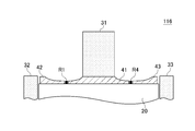
- FIG. 26 is a schematic perspective view for explaining the configuration of the magnetic sensor 119 according to the nineteenth modification.
- the sensor substrate 20 is mounted on the surface of the circuit substrate 10 having an xy plane. That is, the element formation surface 21 of the sensor substrate 20 forms an xz plane, and the first external magnetic body 31 extends in the y direction. According to such a configuration, it is not necessary to provide the opening 11 in the circuit board 10 and the magnetic flux in the direction parallel to the main surface of the circuit board 10 can be selectively detected. Further, even if the height (the length in the y direction) of the first external magnetic body 31 is increased, the support of the first external magnetic body 31 does not become unstable.
Landscapes
- Physics & Mathematics (AREA)
- Condensed Matter Physics & Semiconductors (AREA)
- General Physics & Mathematics (AREA)
- Measuring Magnetic Variables (AREA)
- Hall/Mr Elements (AREA)
Abstract
【課題】4つの感磁素子がブリッジ接続されてなる磁気センサの検出精度を高める。 【解決手段】センサ基板20の表面に設けられた磁性体層41~43と、ブリッジ接続される感磁素子R1~R4とを備える。磁性体層41は、主領域M1と、主領域M1から離れるに従って幅が狭くなる収束領域S1とを含み、磁性体層42は、主領域M2と、主領域M2から離れるに従って幅が狭くなる収束領域S5,S7とを含み、磁性体層43は、主領域M3と、主領域M3から離れるに従って幅が狭くなる収束領域S6,S8とを含む。収束領域S1~S4の端部と収束領域S5~S8の端部は、それぞれギャップG1~G4を介して対向し、感磁素子R1~R4はそれぞれギャップG1~G4によって形成される磁路上に配置される。本発明によれば、各感磁素子に流れる電流によって生じる磁束が他の感磁素子に影響を与えることがないので、検出精度が高められる。
Description
本発明は磁気センサに関し、特に、4つの感磁素子がブリッジ接続されてなる磁気センサに関する。
感磁素子を用いた磁気センサは、電流計や磁気エンコーダなどに広く用いられている。特許文献1に記載されているように、磁気センサには、感磁素子に磁束を集めるための外部磁性体が設けられることがある。しかしながら、特許文献1に記載された磁気センサでは、検出すべき磁束が感磁素子に十分に集中しないことから、検出精度を高めることは困難である。
一方、特許文献2に記載された磁気センサは、感磁素子が形成されるセンサ基板上に磁性体層が設けられており、これにより検出すべき磁束を感磁素子に集中させている。特許文献2に記載された磁気センサでは、3つの磁性体層を用いて2つのギャップを形成し、これら2つのギャップのそれぞれに2つの感磁素子を配置することにより、合計4つの感磁素子によるブリッジ回路を構成している。
しかしながら、特許文献2に記載された磁気センサでは、磁性体層によって形成されるギャップの数が2つであることから、ブリッジ回路を構成する2つの感磁素子が同じギャップ内に配置されることになる。これら2つの感磁素子に流れる電流は、一方が減少すると他方が増加する関係にあることから、一方の感磁素子に流れる電流によって生じる磁束が他方の感磁素子に無視できない影響を与え、その結果、検出精度が低下するおそれがあった。
したがって、本発明は、4つの感磁素子がブリッジ接続されてなる改良された磁気センサを提供することを目的とする。
本発明による磁気センサは、センサ基板と、センサ基板上に設けられた第1、第2及び第3の磁性体層と、ブリッジ接続される第1、第2、第3及び第4の感磁素子と、を備え、前記第1の磁性体層は、第1の主領域と、前記第1の主領域から離れるに従って幅が狭くなる第1、第2、第3及び第4の収束領域とを含み、前記第2の磁性体層は、第2の主領域と、前記第2の主領域から離れるに従って幅が狭くなる第5及び第7の収束領域とを含み、前記第3の磁性体層は、第3の主領域と、前記第3の主領域から離れるに従って幅が狭くなる第6及び第8の収束領域とを含み、前記第1、第2、第3及び第4の収束領域の端部と、前記第5、第6、第7及び第8の収束領域の端部は、それぞれ第1、第2、第3及び第4のギャップを介して対向し、前記第1、第2、第3及び第4の感磁素子は、それぞれ前記第1、第2、第3及び第4のギャップによって形成される磁路上に配置されることを特徴とする。
本発明によれば、4つの感磁素子が互いに異なるギャップによって形成される磁路上に配置されていることから、各感磁素子に流れる電流によって生じる磁束が他の感磁素子に影響を与えることがない。これにより、より検出精度の高い磁気センサを提供することが可能となる。
本発明による磁気センサは、前記第1の主領域を覆うよう、前記センサ基板上に設けられた第1の外部磁性体をさらに備えることが好ましい。これによれば、センサ基板に対して垂直方向の磁束の選択性を高めることができる。
この場合、前記第1乃至第4のギャップの延在方向である第1の方向における前記第1の外部磁性体の幅は、前記第1の主領域の前記第1の方向における幅よりも広く、これにより、前記第1の主領域の前記第1の方向における全幅が前記第1の外部磁性体によって覆われていることが好ましい。これによれば、第1の外部磁性体に位置ずれに起因する検出精度の低下を抑制することが可能となる。
本発明による磁気センサは、前記第2の主領域の近傍に設けられた第2の外部磁性体と、前記第3の主領域の近傍に設けられた第3の外部磁性体とをさらに備えることが好ましい。これによれば、より高い検出精度を得ることが可能となる。
本発明において、前記第1の収束領域と前記第4の収束領域は、前記第1乃至第4のギャップの延在方向である第1の方向に延在する第1の直線を対称軸として線対称であり、前記第2の収束領域と前記第3の収束領域は、前記第1の直線を対称軸として線対称であることが好ましい。これによれば、第1及び第4の感磁素子に印加される磁束のバランス、並びに、第2及び第3の感磁素子に印加される磁束のバランスが高められることから、より高い検出精度を得ることが可能となる。
本発明において、前記第1の収束領域と前記第3の収束領域は、前記第1乃至第4のギャップの延在方向と直交する第2の方向に延在する第2の直線を対称軸として線対称であり、前記第2の収束領域と前記第4の収束領域は、前記第2の直線を対称軸として線対称であり、前記第5の収束領域と前記第7の収束領域は、前記第2の直線を対称軸として線対称であり、前記第6の収束領域と前記第8の収束領域は、前記第2の直線を対称軸として線対称であることが好ましい。これによれば、第1及び第3の感磁素子に印加される磁束のバランス、並びに、第2及び第4の感磁素子に印加される磁束のバランスが高められることから、より高い検出精度を得ることが可能となる。
本発明において、前記第1及び第3の感磁素子は、前記第1及び第2の磁性体層と重なりを有しており、前記第2及び第4の感磁素子は、前記第1及び第3の磁性体層と重なりを有していても構わない。これによれば、漏れ磁束が低減されるため、より高い検出精度を得ることが可能となる。
本発明において、前記第1の磁性体層には、ループ状の外周を有する切り欠き部が設けられていることが好ましい。これによれば、第1の磁性体層の残留磁束が切り欠き部の外周を周回することから、残留磁束による検出精度の低下を防止することが可能となる。
本発明において、前記第1、第2、第3及び第4の感磁素子は、それぞれ前記第1、第2、第3及び第4のギャップによって形成される磁路上に配置された複数の感磁素子が直列接続されてなるものであっても構わない。これによれば、より高い検出精度を得ることが可能となる。
この場合、本発明による磁気センサは、平面視で、前記第1、第2、第3及び第4の感磁素子をそれぞれ構成する前記複数の感磁素子間に配置された第4の磁性体層をさらに備えることが好ましい。これによれば、複数の感磁素子間における漏れ磁束を低減することが可能となる。さらにこの場合、前記第4の磁性体層は、前記第1、第2、第3及び第4の感磁素子をそれぞれ構成する前記複数の感磁素子と重なりを有していても構わない。これによれば、複数の感磁素子間における漏れ磁束をよりいっそう低減することが可能となる。また、前記第4の磁性体層は、前記第1乃至第4のギャップの延在方向である第1の方向に分割されていても構わない。これによれば、第4の磁性体層が磁気的に異方性を持つことから、より高い検出精度を得ることが可能となる。
本発明において、前記第1乃至第4の感磁素子は、いずれも磁気抵抗素子であることが好ましい。この場合、前記第1乃至第4の感磁素子を構成する磁気抵抗素子の感度方向は互いに同一であることが好ましく、前記第1乃至第4の感磁素子を構成する磁気抵抗素子は、スピンバルブ型GMR素子であることが好ましい。
本発明によれば、4つの感磁素子が互いに異なるギャップによって形成される磁路上に配置されることから、これら4つの感磁素子をブリッジ接続することにより、検出精度の高い磁気センサを構成することが可能となる。
以下、添付図面を参照しながら、本発明の好ましい実施形態について詳細に説明する。
図1は、本発明の好ましい実施形態による磁気センサ100の外観を示す略斜視図である。また、図2は磁気センサ100の略分解斜視図であり、図3は図1に示すA-A線に沿った略断面図である。
図1~図3に示すように、本実施形態による磁気センサ100は、開口部11を有する回路基板10と、開口部11に配置されたセンサ基板20と、センサ基板20に固定された第1~第4の外部磁性体31~34とを備えている。センサ基板20は、回路基板10よりも小さいチップ部品であり、後述する感磁素子を有している。また、第1~第4の外部磁性体31~34は、フェライトなど透磁率の高い軟磁性材料からなるブロックである。
センサ基板20は略直方体形状を有し、xy平面を構成する素子形成面21には第1の外部磁性体31が配置されている。センサ基板20の作製方法としては、集合基板に多数のセンサ基板20を同時に形成し、これらを分離することによって多数個取りする方法が一般的であるが、本発明がこれに限定されるものではなく、個々のセンサ基板20を別個に作製しても構わない。詳細については後述するが、素子形成面21には4つの感磁素子R1~R4及び3つの磁性体層41~43が形成されている。また、素子形成面21には4つのボンディングパッド51~54が設けられており、対応するボンディングワイヤBWを介して、回路基板10に設けられたボンディングパッド61~64にそれぞれ接続されている。
さらに、第2及び第3の外部磁性体32,33は、センサ基板20のx方向における両側にそれぞれ配置されている。第2及び第3の外部磁性体32,33は、センサ基板20の底部に位置する第4の外部磁性体34を介して接続されており、これにより第2~第4の外部磁性体32~34は単一の磁性ブロック35を構成する。そして、この磁性ブロック35が回路基板10の開口部11に挿入されるよう配置されている。磁性ブロック35には、センサ基板20を収容するための凹部36が設けられており、この凹部36にセンサ基板20が収容されると、センサ基板20の素子形成面21と、第2及び第3の外部磁性体32,33の先端が近接し、ほぼ同一平面を構成する。
次に、センサ基板20の素子形成面21に形成される各構成要素について詳細に説明する。
図4は、センサ基板20の素子形成面21の構造を説明するための略平面図である。また、図5は、図4に示すB-B線に沿った略断面図である。
図4及び図5に示すように、センサ基板20の素子形成面21には、第1~第3の磁性体層41~43が形成されている。第1の磁性体層41は、素子形成面21の略中央に位置し、そのx方向における両側に第2及び第3の磁性体層42,43が配置される。特に限定されるものではないが、磁性体層41~43としては、樹脂材料に磁性フィラーが分散された複合磁性材料からなる膜であっても構わないし、ニッケル又はパーマロイなどの軟磁性材料からなる薄膜もしくは箔であっても構わないし、フェライトなどからなる薄膜又はバルクシートであっても構わない。
第1の磁性体層41は、中央に位置する第1の主領域M1と、第1の主領域M1からx方向に離れるに従ってy方向における幅が狭くなる第1~第4の収束領域S1~S4を含む。第1の主領域M1は、第1の外部磁性体31によって覆われる部分である。特に限定されるものではないが、第1の外部磁性体31のy方向における幅は、第1の主領域M1のy方向における幅よりも広く、これにより、第1の主領域M1のy方向における全幅が第1の外部磁性体31によって覆われていることが好ましい。これによれば、製造時において、第1の外部磁性体31と第1の外部磁性体31との相対的な位置関係にずれが生じたとしても、検出精度が大幅に低下することがない。位置ずれとしては、xy方向におけるずれの他、回転ずれも考えられる。
上述の通り、第1~第4の収束領域S1~S4は、第1の主領域M1からx方向に離れるに従ってy方向における幅が狭くなるテーパー形状部分であり、本実施形態では、第1及び第3の収束領域S1,S3が第1の主領域M1に対してx方向マイナス側(左側)に位置し、第2及び第4の収束領域S2,S4が第1の主領域M1に対してx方向プラス側(右側)に位置する。
ここで、第1の磁性体層41は二回対称形状を有している。このため、y方向に延在する仮想的な直線L1を対称軸として、第1の収束領域S1と第4の収束領域S4は線対称であり、且つ、第2の収束領域S2と第3の収束領域S3は線対称である。さらに、x方向に延在する仮想的な直線L2を対称軸として、第1の収束領域S1と第3の収束領域S3は線対称であり、且つ、第2の収束領域S4と第4の収束領域S4は線対称である。このような対称形状のため、第1の外部磁性体31を介して取り込まれた磁束が第1の主領域M1に入射されると、図6に示すように、この磁束φが第1~第4の収束領域S1~S4に対してほぼ均等に分配される。そして、分配された磁束φは、テーパー形状を有する第1~第4の収束領域S1~S4を通過することにより、磁束密度が高められる。
一方、第2の磁性体層42は、第2の主領域M2と、第2の主領域M2からx方向(プラス側)に離れるに従ってy方向における幅が狭くなる第5及び第7の収束領域S5,S7を含む。同様に、第3の磁性体層43は、第3の主領域M3と、第3の主領域M3からx方向(マイナス側)に離れるに従ってy方向における幅が狭くなる第6及び第8の収束領域S6,S8を含む。第2の主領域M2は、センサ基板20のx方向マイナス側における端部近傍に位置し、これにより、第2の外部磁性体32と近接する。一方、第3の主領域M3は、センサ基板20のx方向プラス側における端部近傍に位置し、これにより、第3の外部磁性体33と近接する。
第5の収束領域S5の先端部は、第1のギャップG1を介して第1の収束領域S1の先端部と対向している。また、第7の収束領域S7の先端部は、第3のギャップG3を介して第3の収束領域S3の先端部と対向している。ここで、第5の収束領域S5と第7の収束領域S7は、x方向に延在する仮想的な直線L2を対称軸として線対称である。このような対称形状のため、第2の外部磁性体32を介して取り込まれた磁束が第2の主領域M2に入射されると、この磁束が第5及び第7の収束領域S5,S7に対してほぼ均等に分配される。
第6の収束領域S6の先端部は、第2のギャップG2を介して第2の収束領域S2の先端部と対向している。また、第8の収束領域S8の先端部は、第4のギャップG4を介して第4の収束領域S4の先端部と対向している。ここで、第6の収束領域S6と第8の収束領域S8は、x方向に延在する仮想的な直線L2を対称軸として線対称である。このような対称形状のため、第3の外部磁性体33を介して取り込まれた磁束が第3の主領域M3に入射されると、この磁束が第6及び第8の収束領域S6,S8に対してほぼ均等に分配される。
図4に示すように、第1~第4のギャップG1~G4には、それぞれy方向に延在する第1~第4の感磁素子R1~R4が配置されている。第1~第4のギャップG1~G4のx方向における幅は互いに同一である。第1~第4の感磁素子R1~R4は、第1~第3の磁性体層41~43とは接していない。
感磁素子R1~R4は、磁束密度によって物理特性の変化する素子であれば特に限定されないが、磁界の向きに応じて電気抵抗が変化する磁気抵抗素子であることが好ましく、スピンバルブ型GMR素子であることが特に好ましい。本実施形態においては、感磁素子R1~R4の感度方向(固定磁化方向)は、図4及び図5の矢印Cが示す方向(x方向におけるプラス側)に全て揃えられている。
図5に示すように、第1の外部磁性体31はz方向の磁束φを集め、これを第1の磁性体層41の第1の主領域M1に放出する役割を果たす。第1の外部磁性体31のz方向における高さについては特に限定されないが、z方向における高さをより高くすることによって、z方向の磁束の選択性を高めることができる。但し、第1の外部磁性体31のz方向における高さが高すぎると、第1の外部磁性体31の支持が不安定となるおそれがあることから、安定的な支持を確保できる範囲において高くすることが好ましい。
第1の外部磁性体31を介して第1の主領域M1に集められた磁束φは、図6に示すように、第1~第4の収束領域S1~S4に対してほぼ均等に分配された後、第1~第4の感磁素子R1~R4を介してそれぞれ第5~第8の収束領域S5~S8へと放出される。これにより、感磁素子R1,R3と感磁素子R2,R4には、互いに逆方向の磁束が与えられることになる。上述の通り、感磁素子R1~R4の磁化固定方向は、矢印Cが示すxプラス方向に向けられていることから、磁束のx方向における成分に対して感度を持つことになる。
第5及び第7の収束領域S5,S7に到達した磁束は、第2の主領域M2を介して第2の外部磁性体32に回収される。同様に、第6及び第8の収束領域S6,S8に到達した磁束は、第3の主領域M3を介して第3の外部磁性体33に回収される。
図7は、感磁素子R1~R4とボンディングパッド51~54の接続関係を説明するための回路図である。
図7に示すように、ボンディングパッド51,54には、回路基板10側からそれぞれグランド電位Gnd及び電源電位Vddが供給される。また、ボンディングパッド51,54間には、感磁素子R1,R2が直列に接続されるとともに、感磁素子R4,R3が直列に接続される。そして、感磁素子R3,R4の接続点はボンディングパッド52に接続され、感磁素子R1,R2の接続点はボンディングパッド53に接続される。このようなブリッジ接続により、ボンディングパッド53に現れる電位Vaとボンディングパッド52に現れる電位Vbを参照することにより、磁束密度に応じた感磁素子R1~R4の電気抵抗の変化を高感度に検出することが可能となる。
具体的には、感磁素子R1~R4が全て同一の磁化固定方向を有していることから、第1の外部磁性体31からみて一方側に位置する感磁素子R1,R3の抵抗変化量と、第1の外部磁性体31からみて他方側に位置する感磁素子R2,R4の抵抗変化量との間には差が生じる。この差は、図7に示した差動ブリッジ回路によって2倍に増幅され、ボンディングパッド52,53に現れる。回路基板10には、図示しない電圧検出回路が設けられており、ボンディングパッド52,53に現れる電位Va,Vbの差を検出することによって、磁束密度を測定することが可能となる。
そして、本実施形態による磁気センサ100は、センサ基板20の素子形成面21に第1~第3の磁性体層41~43が設けられており、これら磁性体層41~43によって形成される4つのギャップG1~G4にそれぞれ感磁素子R1~R4が配置されていることから、ある感磁素子に流れる電流によって生じる磁束が他の感磁素子に影響を与えることがない。これにより、従来よりも高い検出精度を得ることが可能となる。
しかも、ギャップG1~G4を構成する8つの収束領域S1~S8は、いずれも対応する感磁素子R1~R4に向かって幅が狭くなるテーパー形状を有していることから、感磁素子R1~R4に与えられる磁束の密度が高められる。さらに、第1の磁性体層41に含まれる第1の主領域M1は、4つの収束領域S1~S4の全ての根元部分に接続される広い面積を有していることから、第1の外部磁性体31を介した磁束φの集磁効果が高く、これにより高い検出精度を得ることも可能となる。
また、本実施形態による磁気センサ100は、第1の外部磁性体31を備えていることから、z方向の磁束を選択的に検出することができる。しかも、本実施形態による磁気センサ100は、第2の外部磁性体32と第3の外部磁性体33が一体化されていることから、センサ基板20の背後に回り込む磁束の磁気抵抗を低減することもできる。
以下、本実施形態による磁気センサ100のいくつかの変形例について説明する。
図8は、第1の変形例による磁気センサ101の主要部の構成を説明するための略断面図である。図8に示す例では、センサ基板20の表面に絶縁層22,23がこの順に積層されており、絶縁層22の表面が素子形成面21を構成している。そして、素子形成面21である絶縁層22の表面に感磁素子R1~R4が設けられ、上層に位置する絶縁層23の表面に磁性体層41~43が設けられている。このように、第1の変形例による磁気センサ101では、感磁素子R1~R4と磁性体層41~43が異なる層に位置しており、磁性体層41,42によって形成されるギャップG1(G3)と平面視で重なる位置に感磁素子R1(R3)が配置され、磁性体層41,43によって形成されるギャップG4(G2)と平面視で重なる位置に感磁素子R4(R2)が配置される。第1の変形例による磁気センサ101が例示するように、本発明において、感磁素子R1~R4と磁性体層41~43のz方向における位置は互いに異なっていても構わない。この場合、感磁素子R1~R4は、厳密にはギャップG1~G4間には位置しないが、ギャップG1~G4によって形成される磁路上に配置されることから、ギャップG1~G4を通過する磁束を正しく検出することが可能となる。
図9は、第2の変形例による磁気センサ102の主要部の構成を説明するための略断面図である。図9に示す例では、感磁素子R1(R3)の一部が磁性体層41,42とz方向に重なりを有しており、感磁素子R4(R2)の一部が磁性体層41,43とz方向に重なりを有している。本例においても、感磁素子R1~R4は、厳密にはギャップG1~G4間には位置しないが、ギャップG1~G4によって形成される磁路上に配置されている。このように、感磁素子R1~R4と磁性体層41~43のz方向における位置が互いに異なっている場合、ギャップG1~G4の近傍において両者の一部がz方向に重なるよう配置すれば、漏れ磁束が低減されるため、より高い検出精度を得ることが可能となる。
図10は、第3の変形例による磁気センサ103の主要部の構成を説明するための略断面図である。図10に示す例では、センサ基板20の表面に絶縁層24,25,26がこの順に積層されており、絶縁層25の表面が素子形成面21を構成している。そして、素子形成面21である絶縁層25の表面に感磁素子R1~R4が設けられ、下層に位置する絶縁層24の表面に磁性体層42,43が設けられ、上層に位置する絶縁層26の表面に磁性体層41が設けられている。このように、第3の変形例による磁気センサ103では、磁性体層41と磁性体層42,43が異なる層に位置しており、これらの一部が重なることによって立体的なギャップG1~G4が形成されている。そして、これらギャップG1~G4間に感磁素子R1~R4が配置される構成を有している。第3の変形例による磁気センサ103が例示するように、ギャップG1~G4は平面的なものである必要はなく、立体的なものであっても構わない。
図11は、第4の変形例による磁気センサ104の主要部の構成を説明するための略断面図である。図11に示す例では、磁性体層41と磁性体層42,43が異なる層に位置しており、且つ、互いに重なりを有していない。このため、磁性体層41と磁性体層42,43によって斜め方向のギャップG1~G4が形成され、これらギャップG1~G4に相当する位置に感磁素子R1~R4が配置されている。この場合、感磁素子R1~R4と磁性体層41~43は、重なりを有していても構わないし、重なりを有していなくても構わない。
図12は、第5の変形例による磁気センサ105の主要部の構成を説明するための略断面図である。図12に示す例では、第2の外部磁性体32と第3の外部磁性体33が一体化されておらず、互いに分離されている。このような構成においては、センサ基板20の背後に回り込む磁束の磁気抵抗が若干増加するものの、上述した磁気センサ100とほぼ同様の効果を得ることができる。
図13は、第6の変形例による磁気センサ106の主要部の構成を説明するための略断面図である。図13に示す例では、第2及び第3の外部磁性体32,33が省略されている。このような構成においては、第2及び第3の外部磁性体32,33による集磁効果がなくなるものの、上述した磁気センサ100とほぼ同様の効果を得ることができる。
図14は、第7の変形例による磁気センサ107の主要部の構成を説明するための略平面図である。図14に示す例では、磁性体層41~43にスリットが設けられており、スリットによって磁性体層41~43がそれぞれ複数個に分割されている。具体的には、磁性体層41には十字型のスリットが設けられており、これによって第1~第4の収束領域S1~S4が互いに分離している。また、磁性体層42,43にはx方向に延在するスリットが設けられており、これによって第5及び第7の収束領域S5,S7が互いに分離し、第6及び第8の収束領域S6,S8が互いに分離している。このようなスリットは磁気ギャップとなるものの、その幅が十分に狭ければ、検出精度を十分に確保することが可能となる。第7の変形例による磁気センサ107が例示するように、本発明において、磁性体層41~43のそれぞれが完全に一体的であることは必須でない。
図15は、第8の変形例による磁気センサ108の主要部の構成を説明するための略平面図である。図15に示す例では、第1~第3の磁性体層41~43にいくつかの切り欠き部71が設けられている。切り欠き部71は、ループ状の外周を有する独立したスペースパターンであり、いずれもy方向を長軸方向とする楕円形である。独立したスペースパターンとは、外周が閉じていることを意味する。図15に示す例では、第1の磁性体層41に4つの切り欠き部71が設けられ、第2及び第3の磁性体層42,43にそれぞれ2つの切り欠き部71が設けられている。第1の磁性体層41においては、第1の主領域M1を避けて切り欠き部71が配置されており、これにより第1の主領域M1における集磁効果の低下を防止している。このような切り欠き部71を設ければ、第1~第3の磁性体層41~43の残留磁束が切り欠き部71の外周を周回することから、残留磁束による検出精度の低下を防止することが可能となる。
図16は、第9の変形例による磁気センサ109の主要部の構成を説明するための略平面図である。図16に示す例では、切り欠き部71の内径領域に島状の独立パターン72が設けられている点において、図15に示す例と相違している。独立パターン72は、切り欠き部71を介して第1~第3の磁性体層41~43と分離されている。このような独立パターン72を追加すれば、切り欠き部71を形成することによる磁気抵抗の増加を最小限に抑えることが可能となる。
図17は、第10の変形例による磁気センサ110の主要部の構成を説明するための略平面図である。図17に示す例では、第1の磁性体層41に2つの切り欠き部73が設けられている点において、図15に示す例と相違している。切り欠き部73もループ状の外周を有する独立したスペースパターンであり、いずれもx方向を長軸方向とする楕円形である。このような構成であっても、図15に示す例と同様の効果を得ることができる。
図18は、第11の変形例による磁気センサ111の主要部の構成を説明するための略平面図である。図18に示す例では、切り欠き部73の内径領域に島状の独立パターン74が設けられている点において、図17に示す例と相違している。独立パターン74は、切り欠き部73を介して第1の磁性体層41と分離されている。このような独立パターン74を追加すれば、切り欠き部73を形成することによる磁気抵抗の増加を最小限に抑えることが可能となる。
図19は、第12の変形例による磁気センサ112の主要部の構成を説明するための略平面図である。図19に示す例では、第1~第8の収束領域S1~S8のエッジが曲線的である。このような構成とすれば、第1~第8の収束領域S1~S8における磁束の流れがよりスムーズとなり、磁気抵抗が低下する。
図20は、第13の変形例による磁気センサ113の主要部の構成を説明するための略平面図である。図20に示す例では、第1~第4の感磁素子R1~R4がそれぞれ第1~第4のギャップG1~G4に配置された2つの感磁素子によって構成されている。具体的には、直列接続された2つの感磁素子R11,R12によって第1の感磁素子R1が構成され、直列接続された2つの感磁素子R21,R22によって第2の感磁素子R2が構成され、直列接続された2つの感磁素子R31,R32によって第3の感磁素子R3が構成され、直列接続された2つの感磁素子R41,R42によって第4の感磁素子R4が構成されている。これによれば、より大きな磁気抵抗効果を得ることができるため、センサ基板20のサイズをほとんど大型化することなく、高い検出精度を得ることが可能となる。尚、直列接続される2つの感磁素子(例えばR11とR12)の間には、第4の磁性体層44を追加しても構わない。また、各感磁素子R1~R4を直列接続された3以上の感磁素子によって構成しても構わない。
図21は、第14の変形例による磁気センサ114の主要部の構成を説明するための略断面図である。図21に示す例では、感磁素子R1が2つの感磁素子R11,R12によっているとともに、感磁素子R11の一部が磁性体層41,44と重なりを有し、感磁素子R12の一部が磁性体層42,44と重なりを有している。図示しない他の感磁素子R2~R4についても同様の構成を有している。このように、第4の磁性体層44を設けるとともに、各感磁素子R1~R4と磁性体層41~44が重なるよう配置すれば、漏れ磁束が低減されるため、より高い検出精度を得ることが可能となる。
図22は、第15の変形例による磁気センサ115の主要部の構成を説明するための略平面図である。図22に示す例では、第4の磁性体層44がギャップG1の延在方向であるy方向に多数分割されている。図示しない他のギャップG2~G4上においても同様の構成を有している。このように、第4の磁性体層44をy方向に分割すれば、ギャップG1~G4を介した磁束の流れが感磁方向であるx方向に制限され、y方向にはほとんど流れなくなる。つまり、第4の磁性体層44をy方向に分割することによって磁気的な異方性が生じることから、より高い検出精度を得ることが可能となる。
図23は、第16の変形例による磁気センサ116の主要部の構成を説明するための略断面図である。図23に示す例では、第1~第3の磁性体層41~43の膜厚がギャップG1~G4に向かって連続的に薄くなる構造を有している。このような構成によれば、第1~第4の感磁素子R1~R4に磁束がより集中することから、検出精度を高めることが可能となる。
図24は、第17の変形例による磁気センサ117の主要部の構成を説明するための略断面図である。図24に示す例では、第1~第3の磁性体層41~43の膜厚がギャップG1~G4の近傍において薄くなる段差構造を有している。このような構成であっても、第1~第4の感磁素子R1~R4に磁束がより集中することから、検出精度を高めることが可能となる。
図25は、第18の変形例による磁気センサ118の主要部の構成を説明するための略断面図である。図25に示す例では、第1~第3の磁性体層41~43の膜厚がギャップG1~G4に向かって段階的に薄くなる階段状構造を有している。このような構成であっても、第1~第4の感磁素子R1~R4に磁束がより集中することから、検出精度を高めることが可能となる。
図26は、第19の変形例による磁気センサ119の構成を説明するための略斜視図である。図26に示す例では、xy平面を有する回路基板10の表面にセンサ基板20が横倒しで搭載されている。つまり、センサ基板20の素子形成面21がxz面を構成しており、第1の外部磁性体31がy方向に延在している。このような構成によれば、回路基板10に開口部11を設ける必要がなくなるとともに、回路基板10の主面と平行な方向の磁束を選択的に検出することが可能となる。また、第1の外部磁性体31の高さ(y方向における長さ)を長くしても、第1の外部磁性体31の支持が不安定となることがない。
以上、本発明の好ましい実施形態について説明したが、本発明は、上記の実施形態に限定されることなく、本発明の主旨を逸脱しない範囲で種々の変更が可能であり、それらも本発明の範囲内に包含されるものであることはいうまでもない。
10 回路基板
11 開口部
20 センサ基板
21 素子形成面
22~26 絶縁層
31~34 外部磁性体
35 磁性ブロック
36 凹部
41~44 磁性体層
51~54,61~64 ボンディングパッド
71,73 切り欠き部
72,74 独立パターン
100~119 磁気センサ
BW ボンディングワイヤ
G1~G4 ギャップ
L1,L2 直線
M1~M3 主領域
R1~R4 感磁素子
S1~S8 収束領域
φ 磁束
11 開口部
20 センサ基板
21 素子形成面
22~26 絶縁層
31~34 外部磁性体
35 磁性ブロック
36 凹部
41~44 磁性体層
51~54,61~64 ボンディングパッド
71,73 切り欠き部
72,74 独立パターン
100~119 磁気センサ
BW ボンディングワイヤ
G1~G4 ギャップ
L1,L2 直線
M1~M3 主領域
R1~R4 感磁素子
S1~S8 収束領域
φ 磁束
Claims (15)
- センサ基板と、
センサ基板上に設けられた第1、第2及び第3の磁性体層と、
ブリッジ接続される第1、第2、第3及び第4の感磁素子と、を備え、
前記第1の磁性体層は、第1の主領域と、前記第1の主領域から離れるに従って幅が狭くなる第1、第2、第3及び第4の収束領域とを含み、
前記第2の磁性体層は、第2の主領域と、前記第2の主領域から離れるに従って幅が狭くなる第5及び第7の収束領域とを含み、
前記第3の磁性体層は、第3の主領域と、前記第3の主領域から離れるに従って幅が狭くなる第6及び第8の収束領域とを含み、
前記第1、第2、第3及び第4の収束領域の端部と、前記第5、第6、第7及び第8の収束領域の端部は、それぞれ第1、第2、第3及び第4のギャップを介して対向し、
前記第1、第2、第3及び第4の感磁素子は、それぞれ前記第1、第2、第3及び第4のギャップによって形成される磁路上に配置されることを特徴とする磁気センサ。 - 前記第1の主領域を覆うよう、前記センサ基板上に設けられた第1の外部磁性体をさらに備えることを特徴とする請求項1に記載の磁気センサ。
- 前記第1乃至第4のギャップの延在方向である第1の方向における前記第1の外部磁性体の幅は、前記第1の主領域の前記第1の方向における幅よりも広く、これにより、前記第1の主領域の前記第1の方向における全幅が前記第1の外部磁性体によって覆われていることを特徴とする請求項2に記載の磁気センサ。
- 前記第2の主領域の近傍に設けられた第2の外部磁性体と、前記第3の主領域の近傍に設けられた第3の外部磁性体とをさらに備えることを特徴とする請求項2又は3に記載の磁気センサ。
- 前記第1の収束領域と前記第4の収束領域は、前記第1乃至第4のギャップの延在方向である第1の方向に延在する第1の直線を対称軸として線対称であり、
前記第2の収束領域と前記第3の収束領域は、前記第1の直線を対称軸として線対称であることを特徴とする請求項1乃至4のいずれか一項に記載の磁気センサ。 - 前記第1の収束領域と前記第3の収束領域は、前記第1乃至第4のギャップの延在方向と直交する第2の方向に延在する第2の直線を対称軸として線対称であり、
前記第2の収束領域と前記第4の収束領域は、前記第2の直線を対称軸として線対称であり、
前記第5の収束領域と前記第7の収束領域は、前記第2の直線を対称軸として線対称であり、
前記第6の収束領域と前記第8の収束領域は、前記第2の直線を対称軸として線対称であることを特徴とする請求項1乃至5のいずれか一項に記載の磁気センサ。 - 前記第1及び第3の感磁素子は、前記第1及び第2の磁性体層と重なりを有しており、
前記第2及び第4の感磁素子は、前記第1及び第3の磁性体層と重なりを有していることを特徴とする請求項1乃至6のいずれか一項に記載の磁気センサ。 - 前記第1の磁性体層には、ループ状の外周を有する切り欠き部が設けられていることを特徴とする請求項1乃至7のいずれか一項に記載の磁気センサ。
- 前記第1、第2、第3及び第4の感磁素子は、それぞれ前記第1、第2、第3及び第4のギャップによって形成される磁路上に配置された複数の感磁素子が直列接続されてなることを特徴とする請求項1乃至8のいずれか一項に記載の磁気センサ。
- 平面視で、前記第1、第2、第3及び第4の感磁素子をそれぞれ構成する前記複数の感磁素子間に配置された第4の磁性体層をさらに備えることを特徴とする請求項9に記載の磁気センサ。
- 前記第4の磁性体層は、前記第1、第2、第3及び第4の感磁素子をそれぞれ構成する前記複数の感磁素子と重なりを有していることを特徴とする請求項10に記載の磁気センサ。
- 前記第4の磁性体層は、前記第1乃至第4のギャップの延在方向である第1の方向に分割されていることを特徴とする請求項10又は11に記載の磁気センサ。
- 前記第1乃至第4の感磁素子は、いずれも磁気抵抗素子であることを特徴とする請求項1乃至12のいずれか一項に記載の磁気センサ。
- 前記第1乃至第4の感磁素子を構成する磁気抵抗素子の感度方向は互いに同一であることを特徴とする請求項13に記載の磁気センサ。
- 前記第1乃至第4の感磁素子を構成する磁気抵抗素子は、スピンバルブ型GMR素子であることを特徴とする請求項13又は14に記載の磁気センサ。
Priority Applications (4)
| Application Number | Priority Date | Filing Date | Title |
|---|---|---|---|
| CN201780032067.5A CN109154640B (zh) | 2016-05-24 | 2017-05-22 | 磁传感器 |
| EP17802743.9A EP3467529B1 (en) | 2016-05-24 | 2017-05-22 | Magnetic sensor |
| JP2018519532A JP7014159B2 (ja) | 2016-05-24 | 2017-05-22 | 磁気センサ |
| US16/302,264 US10890630B2 (en) | 2016-05-24 | 2017-05-22 | Magnetic sensor |
Applications Claiming Priority (2)
| Application Number | Priority Date | Filing Date | Title |
|---|---|---|---|
| JP2016-103210 | 2016-05-24 | ||
| JP2016103210 | 2016-05-24 |
Publications (1)
| Publication Number | Publication Date |
|---|---|
| WO2017204151A1 true WO2017204151A1 (ja) | 2017-11-30 |
Family
ID=60412322
Family Applications (1)
| Application Number | Title | Priority Date | Filing Date |
|---|---|---|---|
| PCT/JP2017/019009 Ceased WO2017204151A1 (ja) | 2016-05-24 | 2017-05-22 | 磁気センサ |
Country Status (5)
| Country | Link |
|---|---|
| US (1) | US10890630B2 (ja) |
| EP (1) | EP3467529B1 (ja) |
| JP (1) | JP7014159B2 (ja) |
| CN (1) | CN109154640B (ja) |
| WO (1) | WO2017204151A1 (ja) |
Cited By (22)
| Publication number | Priority date | Publication date | Assignee | Title |
|---|---|---|---|---|
| WO2018216651A1 (ja) * | 2017-05-23 | 2018-11-29 | Tdk株式会社 | 磁気センサ |
| WO2019139110A1 (ja) * | 2018-01-11 | 2019-07-18 | Tdk株式会社 | 磁気センサ |
| JP2019117087A (ja) * | 2017-12-27 | 2019-07-18 | Tdk株式会社 | 磁気センサ |
| JP2019144116A (ja) * | 2018-02-21 | 2019-08-29 | Tdk株式会社 | 磁気センサ |
| JP2019148475A (ja) * | 2018-02-27 | 2019-09-05 | Tdk株式会社 | 磁気センサ |
| JP2019158508A (ja) * | 2018-03-12 | 2019-09-19 | Tdk株式会社 | 磁気センサ |
| JP2019163935A (ja) * | 2018-03-19 | 2019-09-26 | Tdk株式会社 | 磁気センサ |
| JP2019174140A (ja) * | 2018-03-27 | 2019-10-10 | Tdk株式会社 | 磁気センサ |
| JP2019190890A (ja) * | 2018-04-20 | 2019-10-31 | Tdk株式会社 | 磁路形成部材及びこれを用いた磁気センサ |
| WO2019239933A1 (ja) * | 2018-06-11 | 2019-12-19 | Tdk株式会社 | 磁気センサ |
| JP2019215311A (ja) * | 2018-06-07 | 2019-12-19 | Tdk株式会社 | 磁気センサ |
| JP2019219182A (ja) * | 2018-06-15 | 2019-12-26 | Tdk株式会社 | 磁気センサ |
| JP2020067331A (ja) * | 2018-10-23 | 2020-04-30 | Tdk株式会社 | 磁気センサ |
| JP2020071198A (ja) * | 2018-11-02 | 2020-05-07 | Tdk株式会社 | 磁気センサ |
| WO2020137861A1 (ja) * | 2018-12-26 | 2020-07-02 | Tdk株式会社 | 磁気センサ |
| CN112005126A (zh) * | 2018-03-29 | 2020-11-27 | Tdk株式会社 | 磁传感器 |
| JP2021006813A (ja) * | 2018-08-22 | 2021-01-21 | 旭化成エレクトロニクス株式会社 | 磁場計測装置、磁場計測方法、磁場計測プログラム |
| JP2021067568A (ja) * | 2019-10-24 | 2021-04-30 | Tdk株式会社 | 磁気センサ |
| US11237230B1 (en) | 2020-09-14 | 2022-02-01 | Kabushiki Kaisha Toshiba | Magnetic sensor and inspection device |
| JP2023048427A (ja) * | 2021-09-28 | 2023-04-07 | 旭化成エレクトロニクス株式会社 | 磁気センサ |
| JP2023122721A (ja) * | 2022-02-24 | 2023-09-05 | Tdk株式会社 | 磁気センサ |
| US11747303B2 (en) | 2020-12-14 | 2023-09-05 | Kabushiki Kaisha Toshiba | Magnetic sensor and inspection device |
Families Citing this family (8)
| Publication number | Priority date | Publication date | Assignee | Title |
|---|---|---|---|---|
| JP6936405B2 (ja) | 2018-12-26 | 2021-09-15 | 旭化成エレクトロニクス株式会社 | 磁場計測装置 |
| CN111766293A (zh) * | 2019-04-02 | 2020-10-13 | 中国石油天然气集团有限公司 | 多规格连续管缺陷检测装置 |
| JP7375419B2 (ja) * | 2019-09-26 | 2023-11-08 | Tdk株式会社 | 磁気センサ |
| JP7316719B2 (ja) | 2020-08-25 | 2023-07-28 | 株式会社東芝 | 磁気センサ及び検査装置 |
| JP7553388B2 (ja) * | 2021-03-18 | 2024-09-18 | Tdk株式会社 | 磁気センサ |
| US20250164584A1 (en) * | 2022-02-25 | 2025-05-22 | Tdk Corporation | Sensor chip, magnetic sensor having the same, and magnetic sensor manufacturing method |
| JP7746227B2 (ja) * | 2022-07-04 | 2025-09-30 | 株式会社東芝 | センサ及び検査装置 |
| JP7746233B2 (ja) * | 2022-08-09 | 2025-09-30 | 株式会社東芝 | 磁気センサ及び検査装置 |
Citations (8)
| Publication number | Priority date | Publication date | Assignee | Title |
|---|---|---|---|---|
| JPH07210835A (ja) * | 1993-12-14 | 1995-08-11 | Thomson Csf | 磁気抵抗磁気センサ |
| JPH095413A (ja) * | 1995-06-16 | 1997-01-10 | Nec Corp | 磁気センサ |
| JP2005049179A (ja) * | 2003-07-31 | 2005-02-24 | Mitsuteru Kimura | 半導体磁気センサとこれを用いた磁気計測装置 |
| JP2008170368A (ja) * | 2007-01-15 | 2008-07-24 | Mitsubishi Electric Corp | 磁界検出装置および磁界検出装置の製造方法 |
| US20110215800A1 (en) * | 2010-03-05 | 2011-09-08 | Headway Technologies, Inc. | MR sensor with flux guide enhanced hard bias structure |
| JP2013108923A (ja) * | 2011-11-24 | 2013-06-06 | Tdk Corp | 三次元磁界センサおよびその製造方法 |
| US20150028863A1 (en) * | 2013-07-29 | 2015-01-29 | Innovative Micro Technology | Microfabricated magnetic field transducer with flux guide |
| JP2015219061A (ja) * | 2014-05-15 | 2015-12-07 | Tdk株式会社 | 磁界検出センサ及びそれを用いた磁界検出装置 |
Family Cites Families (23)
| Publication number | Priority date | Publication date | Assignee | Title |
|---|---|---|---|---|
| JPS49135587A (ja) * | 1973-04-28 | 1974-12-27 | ||
| FR2754905B1 (fr) * | 1996-10-22 | 1998-11-20 | Commissariat Energie Atomique | Procede de realisation d'un capteur magnetique magnetoresistif et capteur obtenu par ce procede |
| JP2004158668A (ja) * | 2002-11-07 | 2004-06-03 | Asahi Kasei Corp | ハイブリッド磁気センサ及びその製造方法 |
| JP2005159273A (ja) * | 2003-05-27 | 2005-06-16 | Matsushita Electric Works Ltd | 磁電変換素子、磁気検出装置及び地磁気センサ |
| US8378674B2 (en) | 2007-05-28 | 2013-02-19 | Mitsubishi Electric Corporation | Magnetic field detection device |
| JP5500785B2 (ja) | 2008-05-14 | 2014-05-21 | 新科實業有限公司 | 磁気センサ |
| US8451003B2 (en) * | 2009-07-29 | 2013-05-28 | Tdk Corporation | Magnetic sensor having magneto-resistive elements on a substrate |
| CN102435961B (zh) * | 2010-09-28 | 2014-10-08 | 株式会社村田制作所 | 长型磁传感器 |
| JP5494591B2 (ja) | 2010-09-28 | 2014-05-14 | 株式会社村田製作所 | 長尺型磁気センサ |
| CN102280574B (zh) * | 2011-01-07 | 2014-04-16 | 江苏多维科技有限公司 | 薄膜磁电阻传感元件、多个传感元件的组合及与该组合耦合的电子装置 |
| WO2012096132A1 (ja) * | 2011-01-13 | 2012-07-19 | アルプス電気株式会社 | 磁気センサ |
| JP2013172040A (ja) * | 2012-02-22 | 2013-09-02 | Alps Electric Co Ltd | 磁気センサとその製造方法 |
| JP5701807B2 (ja) * | 2012-03-29 | 2015-04-15 | 株式会社東芝 | 圧力センサ及びマイクロフォン |
| CN103116143B (zh) * | 2013-01-22 | 2015-01-14 | 中国人民解放军国防科学技术大学 | 一体式高精度三轴磁传感器 |
| JP6021239B2 (ja) * | 2013-02-13 | 2016-11-09 | マグネデザイン株式会社 | 3次元磁界検出素子および3次元磁界検出装置 |
| JP6190226B2 (ja) * | 2013-09-20 | 2017-08-30 | 株式会社東芝 | 慣性センサ |
| JP6074344B2 (ja) * | 2013-09-20 | 2017-02-01 | 株式会社東芝 | 圧力センサ、マイクロフォン、血圧センサ及びタッチパネル |
| DE102014116953B4 (de) * | 2014-11-19 | 2022-06-30 | Sensitec Gmbh | Verfahren und Vorrichtung zur Herstellung einer Magnetfeldsensorvorrichtung, sowie diesbezüglicheMagnetfeldsensorvorrichtung |
| CN104931900B (zh) * | 2015-06-15 | 2017-12-29 | 中国科学院空间科学与应用研究中心 | 一种基于异常磁阻效应的高灵敏度矢量磁场传感器 |
| JP6480837B2 (ja) * | 2015-09-04 | 2019-03-13 | 株式会社東芝 | センサ、情報端末、マイクロフォン、血圧センサ及びタッチパネル |
| JP6717442B2 (ja) * | 2018-01-25 | 2020-07-01 | 株式会社村田製作所 | 磁気センサおよび電流センサ |
| JP6791237B2 (ja) * | 2018-12-28 | 2020-11-25 | Tdk株式会社 | 磁気センサ装置 |
| JP7006633B2 (ja) * | 2019-02-13 | 2022-01-24 | Tdk株式会社 | 磁気センサシステム |
-
2017
- 2017-05-22 JP JP2018519532A patent/JP7014159B2/ja active Active
- 2017-05-22 WO PCT/JP2017/019009 patent/WO2017204151A1/ja not_active Ceased
- 2017-05-22 US US16/302,264 patent/US10890630B2/en active Active
- 2017-05-22 EP EP17802743.9A patent/EP3467529B1/en active Active
- 2017-05-22 CN CN201780032067.5A patent/CN109154640B/zh active Active
Patent Citations (8)
| Publication number | Priority date | Publication date | Assignee | Title |
|---|---|---|---|---|
| JPH07210835A (ja) * | 1993-12-14 | 1995-08-11 | Thomson Csf | 磁気抵抗磁気センサ |
| JPH095413A (ja) * | 1995-06-16 | 1997-01-10 | Nec Corp | 磁気センサ |
| JP2005049179A (ja) * | 2003-07-31 | 2005-02-24 | Mitsuteru Kimura | 半導体磁気センサとこれを用いた磁気計測装置 |
| JP2008170368A (ja) * | 2007-01-15 | 2008-07-24 | Mitsubishi Electric Corp | 磁界検出装置および磁界検出装置の製造方法 |
| US20110215800A1 (en) * | 2010-03-05 | 2011-09-08 | Headway Technologies, Inc. | MR sensor with flux guide enhanced hard bias structure |
| JP2013108923A (ja) * | 2011-11-24 | 2013-06-06 | Tdk Corp | 三次元磁界センサおよびその製造方法 |
| US20150028863A1 (en) * | 2013-07-29 | 2015-01-29 | Innovative Micro Technology | Microfabricated magnetic field transducer with flux guide |
| JP2015219061A (ja) * | 2014-05-15 | 2015-12-07 | Tdk株式会社 | 磁界検出センサ及びそれを用いた磁界検出装置 |
Non-Patent Citations (1)
| Title |
|---|
| See also references of EP3467529A4 * |
Cited By (43)
| Publication number | Priority date | Publication date | Assignee | Title |
|---|---|---|---|---|
| WO2018216651A1 (ja) * | 2017-05-23 | 2018-11-29 | Tdk株式会社 | 磁気センサ |
| JP2018197661A (ja) * | 2017-05-23 | 2018-12-13 | Tdk株式会社 | 磁気センサ |
| JP2019117087A (ja) * | 2017-12-27 | 2019-07-18 | Tdk株式会社 | 磁気センサ |
| US11237228B2 (en) | 2017-12-27 | 2022-02-01 | Tdk Corporation | Magnetic sensor |
| US11754645B2 (en) | 2017-12-27 | 2023-09-12 | Tdk Corporation | Magnetic sensor |
| US12105165B2 (en) | 2017-12-27 | 2024-10-01 | Tdk Corporation | Magnetic sensor |
| WO2019139110A1 (ja) * | 2018-01-11 | 2019-07-18 | Tdk株式会社 | 磁気センサ |
| JPWO2019139110A1 (ja) * | 2018-01-11 | 2021-01-28 | Tdk株式会社 | 磁気センサ |
| JP2019144116A (ja) * | 2018-02-21 | 2019-08-29 | Tdk株式会社 | 磁気センサ |
| JP2019148475A (ja) * | 2018-02-27 | 2019-09-05 | Tdk株式会社 | 磁気センサ |
| JP7020176B2 (ja) | 2018-02-27 | 2022-02-16 | Tdk株式会社 | 磁気センサ |
| WO2019167598A1 (ja) * | 2018-02-27 | 2019-09-06 | Tdk株式会社 | 磁気センサ |
| JP2019158508A (ja) * | 2018-03-12 | 2019-09-19 | Tdk株式会社 | 磁気センサ |
| JP7077679B2 (ja) | 2018-03-12 | 2022-05-31 | Tdk株式会社 | 磁気センサ |
| JP2019163935A (ja) * | 2018-03-19 | 2019-09-26 | Tdk株式会社 | 磁気センサ |
| JP7192227B2 (ja) | 2018-03-19 | 2022-12-20 | Tdk株式会社 | 磁気センサ |
| JP2019174140A (ja) * | 2018-03-27 | 2019-10-10 | Tdk株式会社 | 磁気センサ |
| JP7095350B2 (ja) | 2018-03-27 | 2022-07-05 | Tdk株式会社 | 磁気センサ |
| US11442120B2 (en) | 2018-03-29 | 2022-09-13 | Tdk Corporation | Magnetic sensor with compensation coil for cancelling magnetic flux applied to a magneto-sensitive element |
| CN112005126A (zh) * | 2018-03-29 | 2020-11-27 | Tdk株式会社 | 磁传感器 |
| EP3779490A4 (en) * | 2018-03-29 | 2021-12-22 | TDK Corporation | MAGNETIC SENSOR |
| JP2019190890A (ja) * | 2018-04-20 | 2019-10-31 | Tdk株式会社 | 磁路形成部材及びこれを用いた磁気センサ |
| JP7070020B2 (ja) | 2018-04-20 | 2022-05-18 | Tdk株式会社 | 磁路形成部材及びこれを用いた磁気センサ |
| JP2019215311A (ja) * | 2018-06-07 | 2019-12-19 | Tdk株式会社 | 磁気センサ |
| JP7115242B2 (ja) | 2018-06-07 | 2022-08-09 | Tdk株式会社 | 磁気センサ |
| WO2019239933A1 (ja) * | 2018-06-11 | 2019-12-19 | Tdk株式会社 | 磁気センサ |
| JP2019215182A (ja) * | 2018-06-11 | 2019-12-19 | Tdk株式会社 | 磁気センサ |
| JP2019219182A (ja) * | 2018-06-15 | 2019-12-26 | Tdk株式会社 | 磁気センサ |
| JP2021006813A (ja) * | 2018-08-22 | 2021-01-21 | 旭化成エレクトロニクス株式会社 | 磁場計測装置、磁場計測方法、磁場計測プログラム |
| JP7402768B2 (ja) | 2018-08-22 | 2023-12-21 | 旭化成エレクトロニクス株式会社 | 磁場計測装置、磁場計測方法、磁場計測プログラム |
| WO2020084953A1 (ja) * | 2018-10-23 | 2020-04-30 | Tdk株式会社 | 磁気センサ |
| JP2020067331A (ja) * | 2018-10-23 | 2020-04-30 | Tdk株式会社 | 磁気センサ |
| JP7147462B2 (ja) | 2018-10-23 | 2022-10-05 | Tdk株式会社 | 磁気センサ |
| JP7115224B2 (ja) | 2018-11-02 | 2022-08-09 | Tdk株式会社 | 磁気センサ |
| JP2020071198A (ja) * | 2018-11-02 | 2020-05-07 | Tdk株式会社 | 磁気センサ |
| WO2020137861A1 (ja) * | 2018-12-26 | 2020-07-02 | Tdk株式会社 | 磁気センサ |
| JP2021067568A (ja) * | 2019-10-24 | 2021-04-30 | Tdk株式会社 | 磁気センサ |
| JP7006670B2 (ja) | 2019-10-24 | 2022-01-24 | Tdk株式会社 | 磁気センサ |
| US11237230B1 (en) | 2020-09-14 | 2022-02-01 | Kabushiki Kaisha Toshiba | Magnetic sensor and inspection device |
| US11747303B2 (en) | 2020-12-14 | 2023-09-05 | Kabushiki Kaisha Toshiba | Magnetic sensor and inspection device |
| JP2023048427A (ja) * | 2021-09-28 | 2023-04-07 | 旭化成エレクトロニクス株式会社 | 磁気センサ |
| JP2023122721A (ja) * | 2022-02-24 | 2023-09-05 | Tdk株式会社 | 磁気センサ |
| JP7824094B2 (ja) | 2022-02-24 | 2026-03-04 | Tdk株式会社 | 磁気センサ |
Also Published As
| Publication number | Publication date |
|---|---|
| JP7014159B2 (ja) | 2022-02-01 |
| US10890630B2 (en) | 2021-01-12 |
| JPWO2017204151A1 (ja) | 2019-03-22 |
| US20190293735A1 (en) | 2019-09-26 |
| CN109154640A (zh) | 2019-01-04 |
| EP3467529A4 (en) | 2020-03-04 |
| EP3467529B1 (en) | 2021-12-01 |
| CN109154640B (zh) | 2021-03-23 |
| EP3467529A1 (en) | 2019-04-10 |
Similar Documents
| Publication | Publication Date | Title |
|---|---|---|
| WO2017204151A1 (ja) | 磁気センサ | |
| EP2682773B1 (en) | Separately packaged bridge magnetic-field angle sensor | |
| CN103995240B (zh) | 一种磁电阻z轴梯度传感器芯片 | |
| US10060941B2 (en) | Magnetoresistive gear tooth sensor | |
| JP6076346B2 (ja) | Mtj三軸磁場センサおよびそのパッケージ方法 | |
| CN110709720B (zh) | 磁传感器 | |
| US9964601B2 (en) | Magnetic sensor | |
| JP6427588B2 (ja) | 磁気センサ | |
| JP6597370B2 (ja) | 磁気センサ | |
| JP2011047929A (ja) | 磁気センサ | |
| CN111693911B (zh) | 磁传感器装置 | |
| CN109655767B (zh) | 一种集成磁结构 | |
| JP6972900B2 (ja) | 磁気センサ | |
| JP7020176B2 (ja) | 磁気センサ | |
| WO2019139110A1 (ja) | 磁気センサ | |
| JP2014182096A (ja) | 磁気センサ | |
| WO2012172946A1 (ja) | 電流センサ | |
| US11815571B2 (en) | Electric current sensor and sensing device | |
| JP2015001467A (ja) | 磁気センサ | |
| KR20230089608A (ko) | 3축 자기저항 센서 | |
| JP2019190890A (ja) | 磁路形成部材及びこれを用いた磁気センサ |
Legal Events
| Date | Code | Title | Description |
|---|---|---|---|
| ENP | Entry into the national phase |
Ref document number: 2018519532 Country of ref document: JP Kind code of ref document: A |
|
| NENP | Non-entry into the national phase |
Ref country code: DE |
|
| 121 | Ep: the epo has been informed by wipo that ep was designated in this application |
Ref document number: 17802743 Country of ref document: EP Kind code of ref document: A1 |
|
| ENP | Entry into the national phase |
Ref document number: 2017802743 Country of ref document: EP Effective date: 20190102 |