WO2017221441A1 - Dispositif de communication optique - Google Patents
Dispositif de communication optique Download PDFInfo
- Publication number
- WO2017221441A1 WO2017221441A1 PCT/JP2016/085621 JP2016085621W WO2017221441A1 WO 2017221441 A1 WO2017221441 A1 WO 2017221441A1 JP 2016085621 W JP2016085621 W JP 2016085621W WO 2017221441 A1 WO2017221441 A1 WO 2017221441A1
- Authority
- WO
- WIPO (PCT)
- Prior art keywords
- temperature
- thermistor
- communication device
- temperature sensor
- optical communication
- Prior art date
- Legal status (The legal status is an assumption and is not a legal conclusion. Google has not performed a legal analysis and makes no representation as to the accuracy of the status listed.)
- Ceased
Links
Images


Classifications
-
- H—ELECTRICITY
- H01—ELECTRIC ELEMENTS
- H01S—DEVICES USING THE PROCESS OF LIGHT AMPLIFICATION BY STIMULATED EMISSION OF RADIATION [LASER] TO AMPLIFY OR GENERATE LIGHT; DEVICES USING STIMULATED EMISSION OF ELECTROMAGNETIC RADIATION IN WAVE RANGES OTHER THAN OPTICAL
- H01S5/00—Semiconductor lasers
- H01S5/02—Structural details or components not essential to laser action
- H01S5/022—Mountings; Housings
- H01S5/0239—Combinations of electrical or optical elements
-
- H—ELECTRICITY
- H01—ELECTRIC ELEMENTS
- H01S—DEVICES USING THE PROCESS OF LIGHT AMPLIFICATION BY STIMULATED EMISSION OF RADIATION [LASER] TO AMPLIFY OR GENERATE LIGHT; DEVICES USING STIMULATED EMISSION OF ELECTROMAGNETIC RADIATION IN WAVE RANGES OTHER THAN OPTICAL
- H01S5/00—Semiconductor lasers
- H01S5/02—Structural details or components not essential to laser action
- H01S5/024—Arrangements for thermal management
-
- H—ELECTRICITY
- H01—ELECTRIC ELEMENTS
- H01S—DEVICES USING THE PROCESS OF LIGHT AMPLIFICATION BY STIMULATED EMISSION OF RADIATION [LASER] TO AMPLIFY OR GENERATE LIGHT; DEVICES USING STIMULATED EMISSION OF ELECTROMAGNETIC RADIATION IN WAVE RANGES OTHER THAN OPTICAL
- H01S5/00—Semiconductor lasers
- H01S5/06—Arrangements for controlling the laser output parameters, e.g. by operating on the active medium
- H01S5/068—Stabilisation of laser output parameters
Definitions
- the present invention relates to an optical communication device, and more particularly to an optical communication device having a coaxial module structure using a CAN type package.
- DWDM Dense Wavelength Division Multiplexing
- the optical signal is transmitted from a laser diode provided in the optical communication device. Since the wavelength of the optical signal output from the laser diode depends on the temperature of the laser diode, it is necessary to keep the temperature of the laser diode constant. At this time, since the temperature of the laser diode cannot be directly measured, the temperature of the laser diode is generally indirectly measured using a thermistor that is a semiconductor element for temperature measurement.
- a thermistor is controlled by controlling the amount of heat generated by a Peltier element, which is a thermoelectric conversion element, based on a temperature signal output from the thermistor.
- a technique for keeping the temperature of the laser diode constant by keeping the temperature is described.
- the wall surface of the cover of the CAN package is in contact with the outside air, and the temperature is almost equal to the ambient temperature (environment temperature) of the optical communication device. Therefore, when the environmental temperature fluctuates, there is a problem of the temperature change that the thermistor receives due to heat radiation from the cover. Conventionally, the following two configurations have been proposed in order to suppress the influence of such an environmental temperature on the thermistor.
- a configuration in which a plate-like member is installed on the upper surface of a pedestal (carrier) on which the thermistor is installed is proposed.
- a configuration in which a plate-like member having the same temperature as the carrier is disposed between the upper surface of the cover and the upper surface of the thermistor, it is possible to suppress the influence of the environmental temperature that the thermistor receives due to thermal radiation from the cover. Thereby, even when environmental temperature fluctuates, the temperature of the thermistor can be stabilized and the temperature of the laser diode can be kept constant.
- An object of the present invention is to provide an optical communication device capable of performing
- the present invention relates to an optical communication device that outputs an optical signal toward an output direction, an optical signal generation unit that generates an optical signal, an output unit that outputs an optical signal generated by the optical signal generation unit, and an optical signal
- a temperature sensor that measures the temperature of the generation unit, a temperature adjustment element that adjusts the temperature of the temperature sensor, a carrier in which the optical signal generation unit and the temperature sensor are installed and having a protrusion, an output unit and a carrier
- the optical signal generator is installed on one side of the protrusion of the carrier, the temperature sensor is installed on the other side of the protrusion of the carrier, and the optical signal generator is an output unit in the output direction. And the temperature sensor, and the optical signal generator and the temperature sensor are spaced apart in the output direction.
- the temperature of the laser diode can be kept constant with the thermistor exposed without using an additional member such as a cover member or a plate-like member between the thermistor and the upper surface of the cover. Can do.
- FIG. 1 is a sectional view of an optical communication device for DWDM according to Embodiment 1 of the present invention.
- the optical communication device 1 has a coaxial module structure using a CAN type package.
- CAN type There are two types of optical communication device packages: CAN type and butterfly type.
- the butterfly type has a box shape as described in Patent Document 2, and is larger than the cylindrical CAN type.
- the butterfly mold since the butterfly mold has a box shape, the manufacturing cost is high because an additional process such as a bending process that is not necessary in the CAN mold is necessary in the manufacturing process.
- the butterfly type structure allows the laser diode and the thermistor to be mounted on the same side of the carrier, which is a block on which they are mounted, so that the temperature of the laser diode using the thermistor can be easily adjusted.
- the CAN type has a can shape (cylindrical), and is smaller in size than the butterfly type and has a simple shape that does not require bending in the manufacturing process.
- the distance from the thermistor to the cover is short because of its small size, the amount of heat entering the thermistor due to thermal radiation or heat conduction from the cover is large, and it is easily affected by the environmental temperature.
- it is difficult to mount the laser diode and the thermistor on the same side of the carrier due to the problem of assembly it is difficult to adjust the temperature of the laser diode using the thermistor compared to the butterfly type.
- the optical communication device 1 is hermetically sealed with a stem 2 and a cover 13 serving as a bottom surface, and a lens 4 is provided on the upper surface of the cover 13 (the y-axis positive surface in FIG. 1).
- the positive direction of the y-axis is the optical signal output direction.
- a plate 12 that is a plate-like member, a Peltier element 7 that is a thermoelectric conversion element, and a carrier 3 that is a metal block are installed on the inner surface of the stem 2 (the y-axis positive surface in FIG. 1) in order from the bottom. Yes.
- the carrier 3 is a material in which a material having a high thermal conductivity such as copper is mixed, and a protrusion 14 is provided toward the upper surface of the cover 13 (the y-axis positive surface in FIG. 1).
- a laser diode 6 is mounted on one surface side (the negative surface side of the x axis in FIG. 1) of the protrusion 14 via a submount 10 as a substrate, and the other surface side of the protrusion 14 (in FIG. 1).
- a thermistor 5 as a temperature measuring element is directly installed with an adhesive such as solder on a horizontal portion (attachment portion) on the positive side of the x-axis.
- the upper surface (the y-axis positive surface in FIG. 1) of the thermistor 5 is located below (the y-axis negative surface in FIG. 1) lower side than the lower surface (y-axis negative surface in FIG. 1).
- the laser diode 6 is disposed between the lens 4 and the thermistor 5 in the output direction of the optical communication device 1, and the laser diode 6 and the thermistor 5 are spaced apart in the output direction. Will be.
- the thermistor 5 since the distance from the thermistor 5 to the cover 13 becomes long, it is suppressed that the thermistor 5 receives the influence of environmental temperature by the thermal radiation and heat conduction from the cover 13, and the temperature of the thermistor 5 can be kept constant. it can.
- the laser diode 6 and the thermistor 5 are arranged apart from each other in the output direction without using an additional member such as a cover member or a plate-like member between the thermistor 5 and the upper surface of the cover 13. Even when fluctuates, the temperature of the laser diode 6 can be kept constant.
- the laser diode 6 is a light emitting element, and outputs an optical signal when current is supplied through a lead wire 8 and a wire (not shown) from a control device (microcontroller) which is an external connection device not shown in FIG. To do.
- the lead wire 8 passes through the stem 2, and a sealing glass 11 is filled between the lead wire 8 and the stem 2.
- the wavelength of the optical signal output from the laser diode 6 is temperature dependent, and the wavelength changes depending on the temperature of the laser diode 6. Since the temperature of the laser diode 6 cannot be directly measured, the thermistor 5 is used for temperature measurement.
- the thermistor 5 is a temperature measuring element whose electric resistance value changes depending on the temperature, and information on the temperature of the laser diode 6 (temperature signal) indirectly measured through the heat conduction between the submount 10 and the carrier 3. ) Is output to the control device via the wire 15 and the lead wire 16.
- the lead wire 16 passes through the stem 2, and a sealing glass 11 is filled between the lead wire 16 and the stem 2.
- the Peltier element 7 is a thermoelectric conversion element, and the temperature is applied to the upper and lower surfaces (surface in the y-axis direction in FIG. 1) of the Peltier element 7 according to the amount of current supplied from the control device via the lead wire 8 and a wire (not shown). A difference can be produced, and either one of the upper and lower surfaces can be a heating surface and the other can be a cooling surface. Moreover, the heating surface and the cooling surface can be interchanged by changing the direction of the current flowing in the Peltier element 7. Using these characteristics, the temperature of the thermistor 5 in contact with the Peltier element 7 via the carrier 3 is adjusted by adjusting the temperature of the upper and lower surfaces of the Peltier element 7 (the surface in the y-axis direction in FIG. 1). Can do.
- FIG. 2 is a schematic diagram showing the configuration of the temperature adjustment circuit (feedback circuit) of the optical communication device 1.
- a control device 20 that is external to the optical communication device 1 and connected to the tips of the lead wires 8 and 16 is supplied with current to the Peltier element 7 based on the difference between the temperature signal received from the thermistor 5 and a predetermined reference temperature signal. The amount is determined and controlled so that the temperature signal received from the thermistor 6 is kept constant.
- FIG. 3 is a flowchart showing the temperature adjustment operation by the temperature adjustment circuit of FIG.
- the control device 20 receives a temperature signal output from the thermistor 5 (S101).
- the control device 20 determines the amount of current to be supplied to the Peltier element 7 so that the thermistor 5 has a desired temperature based on the difference between the received temperature signal and a predetermined reference temperature signal (S102).
- a current is supplied from the control device 20 to the Peltier element 7 (S103), and the temperature of the thermistor 5 is determined by the amount of current flowing through the Peltier element 7 (S104).
- the control device 20 compares the temperature of the thermistor 5 with a desired temperature, and adjusts the amount of current to be supplied to the Peltier element 7 until the temperature of the thermistor 5 reaches the desired temperature (S101 to S105).
- the temperature of the laser diode 6 mounted on the same carrier 3 is determined (S106). Since the wavelength output from the laser diode 6 is temperature-dependent, the wavelength is also determined when the temperature of the laser diode 6 is determined. Therefore, an optical signal having a desired wavelength is output from the laser diode 6 through the lens 4 (S107).
- the upper surface (the y-axis positive surface in FIG. 1) of the thermistor 5 is lower than the lower surface (the y-axis negative surface in FIG. 1) of the laser diode 6 (y in FIG. 1). It is located in the negative axis direction.
- the laser diode 6 is disposed between the lens 4 and the thermistor 5 in the output direction of the optical communication device 1, and the laser diode 6 and the thermistor 5 are spaced apart in the output direction. Will be.
- the distance from the thermistor 5 to the cover 13 is increased, so that the thermistor 5 is prevented from being affected by the environmental temperature due to thermal radiation or heat conduction from the cover 13, and the temperature of the thermistor 5 is kept constant. Can keep.
- the laser diode 6 and the thermistor 5 are arranged apart from each other in the output direction without using an additional member such as a cover member or a plate-like member between the thermistor 5 and the upper surface of the cover 13. Even when fluctuates, the temperature of the laser diode 6 can be kept constant.
- cover shapes for optical communication devices there are two types of cover shapes for optical communication devices, butterfly type and CAN type.
- the butterfly type has a box shape and is larger than the cylindrical CAN type.
- the manufacturing cost is high because an additional process such as a bending process that is not necessary in the CAN mold is necessary in the manufacturing process.
- the distance from the thermistor to the cover is long due to its large size, the amount of heat entering the thermistor due to heat radiation and heat conduction from the cover that is close to the ambient temperature by touching the outside air is small, Less susceptible to environmental temperature.
- the butterfly type structure allows the laser diode and the thermistor to be mounted on the same side of the carrier, so that the temperature of the laser diode using the thermistor can be easily adjusted.
- the CAN type has a can shape (cylindrical), and is smaller in size than the butterfly type and has a simple shape that does not require bending in the manufacturing process, so the manufacturing cost is low.
- the distance from the thermistor to the cover is short because of its small size, the amount of heat entering the thermistor due to thermal radiation or heat conduction from the cover is large, and it is easily affected by the environmental temperature.
- it is difficult to mount the laser diode and the thermistor on the same side of the carrier due to the problem of assembly it is difficult to adjust the temperature of the laser diode using the thermistor compared to the butterfly type.
- an optical communication device for DWDM that requires a laser diode to be maintained at a constant temperature with high accuracy.
- the thermistor 5 since the distance from the thermistor 5 to the cover 13 is increased, the thermistor 5 is affected by the environmental temperature due to thermal radiation and heat conduction from the cover 13. Is suppressed, and the temperature of the thermistor 5 can be kept constant.
- an optical communication device for DWDM can be obtained while using a small and low-cost CAN-type cover.
- the thermistor 5 is arranged so that the position in the y-axis direction of FIG. As a result, the temperature of the laser diode 6 is measured by the thermistor 5 in a state where the thermal resistance between the thermistor 5 and the laser diode 6 is reduced and the temperature difference between the thermistor 5 and the laser diode 6 is minimized.
- the thermistor 5 is configured such that the upper surface of the thermistor 5 (the y-axis positive surface in FIG. 1) is the lower surface of the laser diode 6 (y in FIG. 1).
- the distance from the thermistor 5 to the cover 13 is increased by installing the sensor so that it is below (the negative axis surface) (in the negative y-axis direction in FIG. 1). Therefore, the thermistor 5 is not easily affected by thermal radiation or heat conduction from the upper surface of the cover 13 (the y-axis positive surface in FIG. 1).
- the temperature difference between the thermistor 5 and the laser diode 6 can be kept constant, so that the laser diode 6 can be accurately controlled using the detected temperature of the thermistor 5.
- the temperature of the laser diode 6 can be kept constant.
- the center line with respect to the width of the carrier 3 (z-axis direction in FIG. 1) and the center line with respect to the width of the thermistor 5 (z-axis direction in FIG. 1) are parallel and coincident with each other. This is a preferable condition.
- the two side surfaces of the thermistor 5 since the two side surfaces of the thermistor 5 (the surface parallel to the xy plane in FIG. 1 is located farthest from the side surface of the cover 13), the thermistor 5 is exposed to the ambient temperature from the cover 13.
- the temperature difference between the thermistor 5 and the laser diode 6 can be kept constant even when the environmental temperature fluctuates, so that the laser is detected using the detection temperature of the thermistor 5.
- the diode 6 can be controlled with high accuracy, and the temperature of the laser diode 6 can be kept constant.
- Embodiment 2 an optical communication device according to Embodiment 2 of the present invention will be described.
- the same reference numerals as those in FIG. 1 are the same or similar components, and thus detailed description thereof is omitted.
- FIG. 4 is a cross-sectional view of the optical communication device 201 according to Embodiment 2 of the present invention.
- the ratio of the area of the upper surface of the thermistor 205 (site facing in the y direction in FIG. 4) to the area of one side surface (site facing in the x direction in FIG. 4) of the thermistor 205 having a rectangular parallelepiped shape is It is larger than the first embodiment.
- the area of the upper surface of the thermistor 205 is smaller than the area of one side surface of the thermistor 205 by shortening the height dimension of the thermistor 205 (dimension in the y direction in FIG. 4) as compared with the first embodiment. It is designed to be 2.0 times or more.
- the internal thermal resistance in the y direction of the thermistor 205 in FIG. 4 can be reduced, so that the temperature difference between the upper and lower surfaces of the thermistor 205 can be reduced.
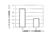
- FIG. 5 is a graph showing the effect of the optical communication device 201 according to the second embodiment of the present invention.
- the horizontal axis in FIG. 5 is a value obtained by dividing the area of the upper surface of the thermistor 205 by the area of one side surface of the thermistor 205.
- the vertical axis in FIG. 5 indicates the temperature difference of the laser diode 6 when the environmental temperature changes.
- the value obtained by dividing the area of the upper surface of the thermistor 205 by the area of one side surface of the thermistor 205 is 1.3.
- the temperature difference is 1.
- the shape of the thermistor 205 By changing the shape of the thermistor 205 to shorten the height dimension of the thermistor 205 and increase the ratio of the area of the upper surface of the thermistor 205 to the area of one side of the thermistor 205, as shown in FIG.
- the temperature difference when the environmental temperature changes can be reduced.
- the thermistor 205 having 2.0 as a value obtained by dividing the upper surface area by the side surface area is used, the thermistor 205 has a value obtained by dividing the upper surface area by the side surface area as 2.
- a shape having 0 or more is preferred. This is because an effect of more than half can be expected for the temperature difference of the laser diode 6 when the environmental temperature changes.
- FIG. 6 is a cross-sectional view of an optical communication device 301 according to Embodiment 3 of the present invention.
- the lower surface (the negative surface in the y-axis direction in FIG. 1) of the submount 10 is above the attachment surface (the negative surface in the y-axis direction in FIG. 1) of the thermistor 5 (the positive y-axis in FIG. 1).
- the lower surface of the submount 310 (the negative surface in the y-axis direction in FIG. 6) is below the attachment surface (the negative surface in the y-axis direction in FIG. 6) of the thermistor 5 (see FIG. 6). 6 in the negative y-axis direction).
- the thickness of the submount 310 (the x-axis direction in FIG. 6) is added to the area serving as the heat transfer path. It spreads by. Thereby, the thermal resistance by the submount 310 and the carrier 3 between the submount 310 and the thermistor 5 can be reduced, and the temperature difference between the submount 310 and the thermistor 5 is reduced.
- FIG. 7 is a cross-sectional view of an optical communication device 401 according to Embodiment 4 of the present invention.
- the lead wire 16 is directly connected to the thermistor 5 through one wire 15.
- a thermal ground 417 as a substrate is installed between the lead wire 16 and the thermistor 5, and the wires 215a and 215b are used to lead the lead wire 16 and the thermal ground 417.
- the thermal ground 417 and the thermistor 5 are electrically connected to each other.
- the thermal ground 417 is a circuit board in which an aluminum nitride layer is subjected to copper, nickel, gold plating or the like, and is attached by solder. Since the tip of the lead wire 16 on the negative side in the y-axis direction in FIG. 7 is in contact with the outside air, the lead wire 16 and the wire 215a attached to the lead wire 16 have a temperature substantially equal to the environmental temperature.
- the thermal ground 417 is installed between the lead wire 16 and the thermistor 5, and the lead wire 16 and the thermal ground 417, and the thermal ground 417 and the thermistor 5 are connected using the wires 415a and 415b, respectively.
- the amount of heat intrusion due to the influence of the environmental temperature transmitted from the wire 415a to the thermistor 5 can be reduced.
- the wire 415a extending from the lead wire 16 into contact with the thermal ground 417, the heat of the wire 415a that is substantially equal to the environmental temperature is transmitted to the carrier 3, and the wire 415a is brought close to the temperature of the carrier 3.
- the wire 415b extending from the thermal ground 417 which is a temperature close to the temperature of the carrier 3, into contact with the thermistor 5, the amount of heat intrusion due to the influence of the environmental temperature transmitted from the wire 415a to the thermistor 5 can be reduced.
- the tip of the lead wire 16 on the outside of the stem 2 (the y-axis negative side in FIG. 7) is in contact with the outside air and becomes a temperature substantially equal to the environmental temperature.
- the thermal ground 417 between the lead wire 16 and the thermistor 5 the heat transferred from the lead wire 16 to the wire 415 a is transferred to the carrier 3 via the thermal ground 417.
- the temperature of the wire 415a connecting the lead wire 16 and the thermal ground 417 is brought close to the temperature of the carrier 3, and the thermal ground 417 and the thermistor 5 are connected by the wire 415b, thereby intruding heat due to the influence of the environmental temperature transmitted to the thermistor 5.
- the amount can be reduced.
- the thermistor 5 can be moved away from the wire 415b having a temperature substantially equal to the environmental temperature. It is possible to reduce the amount of heat intruding into.
Landscapes
- Physics & Mathematics (AREA)
- Condensed Matter Physics & Semiconductors (AREA)
- General Physics & Mathematics (AREA)
- Electromagnetism (AREA)
- Optics & Photonics (AREA)
- Semiconductor Lasers (AREA)
Abstract
Selon l'invention, un dispositif de communication optique comporte : une diode laser qui produit des signaux optiques ; une lentille qui émet les signaux optiques vers l'extérieur ; une thermistance qui mesure la température de la diode laser ; un élément Peltier qui règle la température de la thermistance ; un support ayant une section en saillie ; et un couvercle, qui est pourvu de la lentille, et qui recouvre le support. La diode laser est disposée sur un côté de surface de la section en saillie du support, et la thermistance est disposée sur l'autre côté de surface de la section en saillie du support. La diode laser est disposée entre la lentille et la thermistance dans la direction de sortie, et la diode laser et la thermistance sont disposées en étant séparées l'une de l'autre dans la direction de sortie.
Priority Applications (1)
| Application Number | Priority Date | Filing Date | Title |
|---|---|---|---|
| JP2017525647A JPWO2017221441A1 (ja) | 2016-06-20 | 2016-11-30 | 光通信デバイス |
Applications Claiming Priority (2)
| Application Number | Priority Date | Filing Date | Title |
|---|---|---|---|
| JP2016-121800 | 2016-06-20 | ||
| JP2016121800 | 2016-06-20 |
Publications (1)
| Publication Number | Publication Date |
|---|---|
| WO2017221441A1 true WO2017221441A1 (fr) | 2017-12-28 |
Family
ID=60784671
Family Applications (1)
| Application Number | Title | Priority Date | Filing Date |
|---|---|---|---|
| PCT/JP2016/085621 Ceased WO2017221441A1 (fr) | 2016-06-20 | 2016-11-30 | Dispositif de communication optique |
Country Status (2)
| Country | Link |
|---|---|
| JP (1) | JPWO2017221441A1 (fr) |
| WO (1) | WO2017221441A1 (fr) |
Cited By (1)
| Publication number | Priority date | Publication date | Assignee | Title |
|---|---|---|---|---|
| WO2025182087A1 (fr) * | 2024-03-01 | 2025-09-04 | 三菱電機株式会社 | Module optique |
Citations (6)
| Publication number | Priority date | Publication date | Assignee | Title |
|---|---|---|---|---|
| JPH0475394A (ja) * | 1990-07-18 | 1992-03-10 | Fujitsu Ltd | 半導体レーザモジュール |
| JPH04132286A (ja) * | 1990-09-25 | 1992-05-06 | Fujitsu Ltd | 半導体レーザモジュール及び該モジュールの製造方法 |
| JPH08335747A (ja) * | 1995-06-07 | 1996-12-17 | Anritsu Corp | 発光素子モジュール及びその製造方法 |
| JPH1090077A (ja) * | 1996-09-17 | 1998-04-10 | Fujikura Ltd | 温度制御素子及びこれを用いた電子装置 |
| JP2003142766A (ja) * | 2001-09-06 | 2003-05-16 | Finisar Corp | 組込み式温度制御部付きコンパクトレーザーパッケージ |
| JP2006324524A (ja) * | 2005-05-19 | 2006-11-30 | Sumitomo Electric Ind Ltd | 発光モジュール |
Family Cites Families (2)
| Publication number | Priority date | Publication date | Assignee | Title |
|---|---|---|---|---|
| JP4779747B2 (ja) * | 2006-03-27 | 2011-09-28 | 住友電気工業株式会社 | 発光モジュール |
| JP2008153529A (ja) * | 2006-12-19 | 2008-07-03 | Sumitomo Electric Ind Ltd | 光送信器 |
-
2016
- 2016-11-30 WO PCT/JP2016/085621 patent/WO2017221441A1/fr not_active Ceased
- 2016-11-30 JP JP2017525647A patent/JPWO2017221441A1/ja active Pending
Patent Citations (6)
| Publication number | Priority date | Publication date | Assignee | Title |
|---|---|---|---|---|
| JPH0475394A (ja) * | 1990-07-18 | 1992-03-10 | Fujitsu Ltd | 半導体レーザモジュール |
| JPH04132286A (ja) * | 1990-09-25 | 1992-05-06 | Fujitsu Ltd | 半導体レーザモジュール及び該モジュールの製造方法 |
| JPH08335747A (ja) * | 1995-06-07 | 1996-12-17 | Anritsu Corp | 発光素子モジュール及びその製造方法 |
| JPH1090077A (ja) * | 1996-09-17 | 1998-04-10 | Fujikura Ltd | 温度制御素子及びこれを用いた電子装置 |
| JP2003142766A (ja) * | 2001-09-06 | 2003-05-16 | Finisar Corp | 組込み式温度制御部付きコンパクトレーザーパッケージ |
| JP2006324524A (ja) * | 2005-05-19 | 2006-11-30 | Sumitomo Electric Ind Ltd | 発光モジュール |
Cited By (1)
| Publication number | Priority date | Publication date | Assignee | Title |
|---|---|---|---|---|
| WO2025182087A1 (fr) * | 2024-03-01 | 2025-09-04 | 三菱電機株式会社 | Module optique |
Also Published As
| Publication number | Publication date |
|---|---|
| JPWO2017221441A1 (ja) | 2018-06-21 |
Similar Documents
| Publication | Publication Date | Title |
|---|---|---|
| US12560479B2 (en) | Light detection device | |
| US20070237196A1 (en) | Light-emitting module installing thermo-electric controller | |
| CN103534566B (zh) | 利用热敏电阻测定温度的方法 | |
| US20090059979A1 (en) | Optical transmission module and optical transmission system | |
| JP2018195752A (ja) | 発光装置 | |
| CN104350652A (zh) | 具有波长稳定化装置的激光装置 | |
| WO2017221441A1 (fr) | Dispositif de communication optique | |
| US10886700B2 (en) | Optical module control method, optical module unit, and optical module | |
| US20070127874A1 (en) | Optical module with thermo-electric controller in co-axial package | |
| JP5005421B2 (ja) | 波長ロッカー用温度制御装置、波長ロッカー及び光モジュール | |
| JP5088866B2 (ja) | 波長ロッカー用温度制御装置、波長ロッカー及び光モジュール | |
| JP4779747B2 (ja) | 発光モジュール | |
| KR101514243B1 (ko) | 광원장치 | |
| JP2008153529A (ja) | 光送信器 | |
| KR20030096838A (ko) | 서브마운트 일체형 포토다이오드 및 이를 이용한 레이져다이오드 패키지 | |
| JP2020077773A (ja) | 光源装置 | |
| KR101170937B1 (ko) | 광통신용 광모듈 | |
| JP7774766B2 (ja) | 光モジュール | |
| JP2011243819A (ja) | 同軸型光モジュール | |
| WO2023203774A1 (fr) | Dispositif laser à semi-conducteur | |
| JP2007324234A (ja) | 発光モジュール | |
| JP2009065083A (ja) | 光モジュール | |
| WO2022244440A1 (fr) | Module optique et système de module optique | |
| JP2021125539A (ja) | 光学装置 | |
| JP2011086832A (ja) | 波長ロッカー |
Legal Events
| Date | Code | Title | Description |
|---|---|---|---|
| ENP | Entry into the national phase |
Ref document number: 2017525647 Country of ref document: JP Kind code of ref document: A |
|
| 121 | Ep: the epo has been informed by wipo that ep was designated in this application |
Ref document number: 16906357 Country of ref document: EP Kind code of ref document: A1 |
|
| NENP | Non-entry into the national phase |
Ref country code: DE |
|
| 122 | Ep: pct application non-entry in european phase |
Ref document number: 16906357 Country of ref document: EP Kind code of ref document: A1 |