WO2017221607A1 - Dispositif à semi-conducteur optique avec couche de phosphore - Google Patents
Dispositif à semi-conducteur optique avec couche de phosphore Download PDFInfo
- Publication number
- WO2017221607A1 WO2017221607A1 PCT/JP2017/019060 JP2017019060W WO2017221607A1 WO 2017221607 A1 WO2017221607 A1 WO 2017221607A1 JP 2017019060 W JP2017019060 W JP 2017019060W WO 2017221607 A1 WO2017221607 A1 WO 2017221607A1
- Authority
- WO
- WIPO (PCT)
- Prior art keywords
- white
- optical semiconductor
- phosphor
- layer
- phosphor layer
- Prior art date
- Legal status (The legal status is an assumption and is not a legal conclusion. Google has not performed a legal analysis and makes no representation as to the accuracy of the status listed.)
- Ceased
Links
Images


Classifications
-
- H—ELECTRICITY
- H10—SEMICONDUCTOR DEVICES; ELECTRIC SOLID-STATE DEVICES NOT OTHERWISE PROVIDED FOR
- H10H—INORGANIC LIGHT-EMITTING SEMICONDUCTOR DEVICES HAVING POTENTIAL BARRIERS
- H10H20/00—Individual inorganic light-emitting semiconductor devices having potential barriers, e.g. light-emitting diodes [LED]
- H10H20/80—Constructional details
- H10H20/85—Packages
Definitions
- the present invention relates to an optical semiconductor element with a phosphor layer.
- a light-emitting device such as a white light-emitting device that includes a light-emitting diode element and a phosphor layer and emits white light is known (for example, see Patent Document 1).
- the light emitting device of Patent Document 1 includes a diode substrate, a light emitting diode element flip-chip mounted on the diode substrate, a phosphor layer in direct contact with the upper surface of the light emitting diode element, and a side surface of the light emitting diode element. And a reflective resin layer in direct contact.
- An object of the present invention is to provide a phosphor layer-attached optical semiconductor element having excellent junction reliability and heat dissipation while maintaining good brightness.
- the present invention [1] includes an optical semiconductor element having a light emitting surface and an opposing surface disposed to be opposed to the light emitting surface at an interval in a vertical direction, a white film disposed on the upper side of the light emitting surface, A phosphor layer disposed on the upper side of the white film, wherein the white film has a thickness of 2 ⁇ m or more and 15 ⁇ m or less.
- the present invention [2] includes the optical semiconductor element with a phosphor layer according to [1], wherein the white film has a thickness of 2 ⁇ m or more and 7 ⁇ m or less.
- the present invention [3] includes the optical semiconductor element with a phosphor layer according to [1] or [2], further comprising a white portion arranged around the optical semiconductor element.
- the white film includes the optical semiconductor element with a phosphor layer according to any one of [1] to [3] containing white particles.
- the present invention [5] includes the optical semiconductor element with a phosphor layer according to [4], wherein the white particles have an average particle diameter of 0.1 ⁇ m or more and 2.0 ⁇ m or less.
- the phosphor layer-coated optical semiconductor element of the present invention has excellent bonding reliability and heat dissipation while maintaining good brightness.
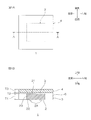
- FIG. 1A to 1B show a first embodiment of an optical semiconductor device with a phosphor layer according to the present invention.
- FIG. 1A is a plan view
- FIG. 1B is a cross-sectional view taken along line AA of FIG. 1A.
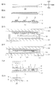
- 2A to 2G are process diagrams of the method of manufacturing the optical semiconductor element with a phosphor layer shown in FIG. 1,
- FIG. 2A is a process for preparing a phosphor laminated sheet
- FIG. 2B is a process for preparing a temporary fixing sheet
- FIG. FIG. 2D shows an opposing placement process
- FIG. 2E shows a stacking process
- FIG. 2F shows a cutting process
- FIG. 2G shows a mounting process.
- FIG. 1A to 1B show a first embodiment of an optical semiconductor device with a phosphor layer according to the present invention.
- FIG. 1A is a plan view
- FIG. 1B is a cross-sectional view taken along line AA of FIG. 1A.
- FIG. 3 is a modification of the first embodiment, and shows a cross-sectional view of a mode in which a light diffusion layer is provided on the upper surface of the phosphor layer.
- 4A to 4F are modifications of the method of manufacturing the optical semiconductor element with a phosphor layer shown in FIG. 1.
- FIG. 4A is a temporary fixing sheet preparation step
- FIG. 4B is a temporary fixing step
- FIG. Resin composition arranging step
- FIG. 4D shows a white layer lamination step
- FIG. 4E shows a step of obtaining a white layer laminate
- FIG. 4F shows a thickness adjustment step.
- FIGS. 5G to 5H are modifications of the method for manufacturing the optical semiconductor device with a phosphor layer shown in FIG. 1 following FIG. 4,
- FIG. 5G shows a phosphor layer laminating step, and
- FIG. 5H shows a cutting step.
- FIG. 6 shows a cross-sectional view of a second embodiment of the optical semiconductor device with a phosphor layer
- the vertical direction of the paper is the vertical direction (first direction, thickness direction)
- the upper side of the paper is the upper side (one side in the first direction, the one side in the thickness direction)
- the lower side of the paper is the lower side (the other side in the first direction).
- the other side in the thickness direction The left-right direction on the paper surface is the left-right direction (second direction orthogonal to the first direction, an example of the orthogonal direction to the up-down direction)
- the left side of the paper is the left side (second side in the second direction)
- the right side of the paper is the right side (the other in the second direction).
- the paper thickness direction is the front-rear direction (the third direction orthogonal to the first direction and the second direction, an example of the orthogonal direction to the vertical direction), the front side of the paper is the front side (one side in the third direction), and the back side of the paper is the rear side (The other side in the third direction). Specifically, it conforms to the direction arrow in each figure.
- a phosphor layer-attached optical semiconductor element 1 (hereinafter also referred to as a layered element) according to a first embodiment of the present invention will be described.
- the layered element 1 is not the optical semiconductor device 16 (light emitting device; see FIG. 2G for reference), that is, the diode substrate 15 (electrode substrate; reference symbol for FIG. 2G) provided in the optical semiconductor device 16. ) Is not included.
- the layered element 1 includes an optical semiconductor element 2, a white layer 3, and a phosphor layer 4.
- the layered element 1 is preferably composed of an optical semiconductor element 2, a white layer 3 and a phosphor layer 4. That is, the layered element 1 is configured such that it is not yet electrically connected to the electrode provided on the diode substrate 15 of the optical semiconductor device 16.
- the layered element 1 is a component for manufacturing the optical semiconductor device 16, that is, a component for manufacturing the optical semiconductor device 16.
- the layered element 1 includes an optical semiconductor element 2, a white layer 3, and a phosphor layer 4.
- the optical semiconductor element 2 is, for example, an LED (light emitting diode element) or an LD (semiconductor laser element) that converts electrical energy into light energy.
- the optical semiconductor element 2 is a blue LED that emits blue light.
- the optical semiconductor element 2 does not include a rectifier (semiconductor element) such as a transistor having a technical field different from that of the optical semiconductor element.
- the optical semiconductor element 2 has a substantially flat plate shape along the left-right direction and the front-rear direction.
- the optical semiconductor element 2 has a substantially rectangular shape in plan view (preferably, a substantially square shape in plan view).
- the optical semiconductor element 2 includes a light emitting surface 21, a facing surface 22, and a side surface 23.
- the light emitting surface 21 is the upper surface of the optical semiconductor element 2.
- the light emitting surface 21 has a flat shape.
- a white film 5 (described later) is provided on the light emitting surface 21.
- the facing surface 22 is a lower surface of the optical semiconductor element 2 and is a surface on which the electrode 24 is provided.
- the facing surface 22 is disposed to face the light emitting surface 21 with a space on the lower side.
- a plurality (two) of the electrodes 24 are provided and have a shape that slightly protrudes downward from the facing surface 22.
- the side surface 23 connects the peripheral edge of the light emitting surface 21 and the peripheral edge of the facing surface 22.
- the thickness T1 (length in the vertical direction) is, for example, 0.1 ⁇ m or more, preferably 1 ⁇ m or more, more preferably 10 ⁇ m or more. For example, it is 500 micrometers or less, Preferably, it is 200 micrometers or less.
- the length in the left-right direction and / or the front-rear direction of the optical semiconductor element 2 is, for example, 200 ⁇ m or more, preferably 500 ⁇ m or more, and for example, 3000 ⁇ m or less, preferably 2000 ⁇ m or less.
- the white layer 3 is a white reflective layer which is disposed on the upper side and the side of the optical semiconductor element 2 and can reflect light emitted from the optical semiconductor element 2 mainly to the side. Specifically, the white layer 3 is in contact with and covers the light emitting surface 21 and the side surface 23 of the optical semiconductor element. Further, the white layer 3 is disposed below the phosphor layer 4. Specifically, the white layer 3 is in contact with and covers the lower surface of the phosphor layer 4.
- the white layer 3 is integrally provided with a white film 5 and a white side portion 6 as a white portion.
- the white film 5 is disposed on the light emitting surface 21 of the optical semiconductor element 2. Specifically, the entire lower surface of the white film 5 is in contact with the entire upper surface of the light emitting surface 21, and the entire upper surface of the white film 5 is in contact with a part (center portion) of the lower surface of the phosphor layer 4. Arranged between the optical semiconductor element 2 and the phosphor layer 4.
- the white film 5 has a substantially flat plate shape along the left-right direction and the front-rear direction, and has a substantially rectangular shape in plan view (preferably, a substantially square shape in plan view).
- the white film 5 is formed so as to coincide with the light emitting surface 21 when projected in the thickness direction.
- the thickness T2 of the white film 5 is 2 ⁇ m or more and 15 ⁇ m or less. From the viewpoint of brightness, heat dissipation, etc., it is preferably 4 ⁇ m or more, and preferably 7 ⁇ m or less.
- the ratio (T2 / T1) of the thickness T2 of the white film 5 to the thickness T1 of the optical semiconductor element 2 is, for example, 0.001 or more, preferably 0.005 or more, and, for example, 0.300 or less, Preferably, it is 0.200 or less.
- the white side portion 6 is arranged on the side of the white film 5 and the optical semiconductor element 2 (around, that is, the outside in the left-right direction and the outside in the front-rear direction). Specifically, the white side portion 6 is disposed so as to contact the entire peripheral end surface of the white film 5 and the entire side surface 23 of the optical semiconductor element 2.
- the white side portion 6 has a substantially rectangular frame shape in plan view.
- the white side portion 6 is formed so that its inner shape matches the shape of the optical semiconductor element 2 and its outer shape matches the shape of the phosphor layer 4 when projected in the thickness direction.
- the thickness of the white side portion 6 is the same as the sum of the thickness T1 of the optical semiconductor element 2 and the thickness T2 of the white film 5.
- the white layer 3 has a reflectance of 70% or more, preferably 80% or more, more preferably 90% or more, for example, 100% when irradiated with light having a wavelength of 450 nm with a thickness of 100 ⁇ m. It is as follows. By setting the reflectance within the above range, the light extraction efficiency can be improved.
- the method for measuring the reflectance can be obtained by measuring the reflectance at a wavelength of 450 nm using an ultraviolet-visible near-infrared spectrophotometer with an optical path confirmation method using an integrating sphere.
- the white layer 3 is formed (prepared) from, for example, a white resin composition containing white particles and a resin.
- the white layer 3 is formed from a white resin composition composed of white particles and a resin.
- white particles examples include white inorganic particles and white organic particles.
- white inorganic particles are used from the viewpoint of heat dissipation and durability.
- Examples of the material constituting the white inorganic particles include oxides such as titanium oxide, zinc oxide, zirconium oxide, and aluminum oxide, such as carbonates such as lead white (basic lead carbonate) and calcium carbonate, such as kaolin. Clay minerals. From the viewpoints of brightness and heat dissipation, an oxide is preferable, and titanium oxide is more preferable.
- the average particle diameter of the white particles is, for example, 0.1 ⁇ m or more, preferably 0.2 ⁇ m or more, and for example, 2.0 ⁇ m or less, preferably 0.5 ⁇ m or less.
- the average particle diameter of the particles is calculated as a D50 value, and specifically measured by a laser diffraction particle size distribution meter.
- the content ratio of the white particles is, for example, 3% by mass or more, preferably 5% by mass or more, more preferably 10% by mass or more, and, for example, 70% by mass or less with respect to the white resin composition. Preferably, it is 50 mass% or less, More preferably, it is 40 mass% or less.
- the resin is a matrix that uniformly disperses white particles in the white resin composition, and is preferably a transparent resin.
- the resin include a curable resin and a thermoplastic resin.
- a curable resin is used.
- curable resin examples include silicone resin, epoxy resin, urethane resin, polyimide resin, phenol resin, urea resin, melamine resin, and unsaturated polyester resin.
- thermosetting resins such as a two-stage reaction curable resin and a one-stage reaction curable resin.
- the two-stage reaction curable resin has two reaction mechanisms.
- the A stage state is changed to the B stage (semi-cured), and then in the second stage reaction, the B stage state is obtained.
- C-stage complete curing
- the two-stage reaction curable resin is a thermosetting resin that can be in a B-stage state under appropriate heating conditions.
- the B stage state (semi-cured state) is a state between the A stage state (uncured state) in which the thermosetting resin is liquid and the fully cured C stage state (completely cured state).
- the gelation is slightly progressed, and the compression elastic modulus is a semi-solid state or a solid state smaller than the compression elastic modulus in the C stage state.
- the first stage reaction curable resin has one reaction mechanism, and can be changed from the A stage state to the C stage by the first stage reaction.
- a one-stage reaction curable resin can stop the reaction in the middle of the first-stage reaction and change from the A-stage state to the B-stage state.
- the reaction is restarted and includes a thermosetting resin that can be changed from the B-stage state to the C-stage. That is, the first-stage reaction curable resin includes a thermosetting resin that can be in a B-stage state.
- the one-stage reaction curable resin cannot be controlled so as to stop in the middle of the one-stage reaction, that is, cannot enter the B stage state, and is thermosetting that changes from the A stage to the C stage at a time. Also includes resin.
- thermosetting resin includes thermosetting resins (two-stage reaction curable resin and one-stage reaction curable resin) that can be in a B-stage state.
- thermosetting resin that can be in the B-stage state
- a silicone resin and an epoxy resin are used, and more preferably, a silicone resin is used.
- silicone resin examples include, for example, a silicone resin having both thermoplasticity and thermosetting properties (thermoplastic / thermosetting silicone resin), no thermoplasticity, and thermosetting properties. Silicone resin (non-thermoplastic / thermosetting silicone resin).
- thermoplastic / thermosetting silicone resin is once plasticized (or liquefied) by heating in the B stage and then cured (C stage) by further heating.
- the one-step reaction curable resin include phenyl silicone resin compositions described in, for example, JP-A-2016-37562.
- the two-step reaction curable resin include JP-A-2014 2014. -72351, JP-A-2013-187227, first to sixth thermoplastic / thermosetting silicone resin compositions (for example, compositions containing both terminal amino-type silicone resins, cage-type octaves) And compositions containing silsesquioxane).
- the phenyl silicone resin composition has a phenyl group in the main skeleton which is a siloxane bond.
- the phenyl silicone resin composition is preferably an addition reaction curable silicone resin composition. Specifically, it contains an alkenyl group-containing polysiloxane, a hydrosilyl group-containing polysiloxane, and a hydrosilylation catalyst, and at least one of the alkenyl group-containing polysiloxane and the hydrosilyl group-containing polysiloxane has a phenyl group.
- a silicone resin composition etc. are mentioned.
- phenyl silicone resin composition examples include “OE-6630” manufactured by Dow Corning, in addition to the phenyl silicone resin composition described in the above publication.
- non-thermoplastic / thermosetting silicone resin as the two-stage reaction curable resin, for example, the first to eighth condensation / reduction resins described in JP2010-265436A, JP2013-187227A, and the like.
- An addition reaction curable silicone resin composition may be mentioned.
- thermoplastic / thermosetting silicone resin is preferable, and a phenyl silicone resin composition is more preferable.
- thermosetting silicone resins that do not take the B stage state include methyl silicone resins such as ELASTOSIL series (manufactured by Asahi Kasei Wacker Silicone, specifically ELASTOSIL LR7665) and KER series (manufactured by Shin-Etsu Silicone). Examples thereof include a composition.
- Resin can be used alone or in combination of two or more.
- the resin content is the balance of the content of the white particles (and additives to be described later), and is, for example, 30% by mass or more, preferably 50% by mass or more, more preferably with respect to the white resin composition. Is 60% by mass or more, and is, for example, 97% by mass or less, preferably 95% by mass or less, and more preferably 90% by mass or less.
- the white resin composition can contain particles other than white particles.
- Examples of such particles include light diffusing inorganic particles.
- Examples of the light diffusing inorganic particles include silica particles and composite inorganic oxide particles (such as glass particles).
- the composite inorganic oxide particles contain, for example, silica or silica and boron oxide as main components, and also include aluminum oxide, calcium oxide, zinc oxide, strontium oxide, magnesium oxide, zirconium oxide, barium oxide, antimony oxide, and the like. Is contained as a minor component.
- the content ratio of the main component in the composite inorganic oxide particles is, for example, 40% by mass or more, preferably 50% by mass or more, and for example, 90% by mass or less, preferably with respect to the composite inorganic oxide particles. 80% by mass or less.
- the content ratio of the subcomponent is the remainder of the content ratio of the main component described above.
- the light diffusing inorganic particles are preferably silica particles from the viewpoint of heat dissipation and brightness.
- the average particle size of the light diffusing inorganic particles is preferably larger than the average particle size of the white particles, specifically, for example, 1.0 ⁇ m or more, preferably 2.0 ⁇ m or more. It is 10 ⁇ m or less, preferably 5.0 ⁇ m or less, and more preferably 3.0 ⁇ m or less.
- the content ratio of the light diffusing inorganic particles is, for example, 1% by mass or more, preferably 5% by mass or more, more preferably 10% by mass or more with respect to the white resin composition. It is 70 mass% or less, Preferably, it is 50 mass% or less, More preferably, it is 30 mass% or less.
- the heat dissipation can be improved while reducing the resin content.
- the particles are preferably composed only of white particles from the viewpoint of heat dissipation, that is, do not contain particles other than white particles. It is preferable.
- the white resin composition may contain a known additive in an appropriate ratio.
- the phosphor layer 4 is a layer containing a phosphor, and is disposed on the upper side of the white film 5. Specifically, the phosphor layer 4 is disposed on the upper surface of the white layer 3 so that the entire lower surface of the phosphor layer 4 is in contact with the entire upper surface of the white layer 3 (the white film 5 and the white side portion 6). Yes.
- the phosphor layer 4 has a substantially flat plate shape along the left-right direction and the front-rear direction, and has a substantially rectangular shape in plan view (preferably, a substantially square shape in plan view).
- the phosphor layer 4 is formed so as to coincide with the white layer 3 when projected in the vertical direction. That is, the peripheral side surface of the phosphor layer 4 is flush with the peripheral side surface of the white side portion 6.
- the thickness T3 of the phosphor layer 4 is, for example, 30 ⁇ m or more, preferably 50 ⁇ m or more, and, for example, 500 ⁇ m or less, preferably 200 ⁇ m or less.
- the ratio (T2 / T3) of the thickness T2 of the white film 5 to the thickness T3 of the phosphor layer 4 is, for example, 0.004 or more, preferably 0.01 or more, and, for example, 0.5 or less, Preferably, it is 0.3 or less.
- the phosphor layer 4 is made of, for example, a sheet-like phosphor-containing cured resin or a phosphor ceramic plate.
- the phosphor-containing cured resin is, for example, a completely cured product (C stage state) of a phosphor resin composition containing a phosphor and a curable resin.
- the phosphor converts the wavelength of the light emitted from the optical semiconductor element 2.
- Examples of the phosphor include a yellow phosphor that can convert blue light into yellow light, and a red phosphor that can convert blue light into red light.
- yellow phosphor examples include silicate phosphors such as (Ba, Sr, Ca) 2 SiO 4 ; Eu, (Sr, Ba) 2 SiO 4 : Eu (barium orthosilicate (BOS)), for example, Y 3 Al Garnet-type phosphors having a garnet-type crystal structure such as 5 O 12 : Ce (YAG (yttrium, aluminum, garnet): Ce), Tb 3 Al 3 O 12 : Ce (TAG (terbium, aluminum, garnet): Ce) Examples thereof include oxynitride phosphors such as Ca- ⁇ -SiAlON.
- silicate phosphors such as (Ba, Sr, Ca) 2 SiO 4 ; Eu, (Sr, Ba) 2 SiO 4 : Eu (barium orthosilicate (BOS)
- Y 3 Al Garnet-type phosphors having a garnet-type crystal structure such as 5 O 12 : Ce (YAG (yttrium, aluminum, garnet): Ce
- red phosphor examples include nitride phosphors such as CaAlSiN 3 : Eu and CaSiN 2 : Eu.
- the phosphor contained in the phosphor-containing cured resin is a particle, and examples of the shape thereof include a spherical shape, a plate shape, and a needle shape.
- the average value of the maximum length of the phosphor (in the case of a sphere, the average particle diameter) is, for example, 0.1 ⁇ m or more, preferably 1 ⁇ m or more, and for example, 200 ⁇ m or less, preferably 100 ⁇ m or less. It is.
- Fluorescent substances can be used alone or in combination of two or more.
- the content ratio of the phosphor is, for example, 10% by mass or more, preferably 20% by mass or more, and, for example, 80% by mass or less, preferably 70% by mass or less with respect to the phosphor resin composition. is there.
- the curable resin is a matrix in which the phosphor is uniformly dispersed in the phosphor resin composition.
- a curable resin include the same curable resins as those exemplified in the white resin composition, preferably a silicone resin, and more preferably a thermoplastic / thermosetting silicone resin. More preferably, a phenyl type silicone resin composition is mentioned.
- the content of the curable resin is the balance of the content of the phosphor (and additive), and is, for example, 20% by mass or more, preferably 30% by mass or more, with respect to the phosphor resin composition. For example, it is 90 mass% or less, Preferably, it is 80 mass% or less.
- the phosphor resin composition may contain a known additive such as inorganic particles in an appropriate ratio.
- the inorganic particles include the light diffusing inorganic particles described above for the white resin composition, preferably silica particles and glass particles, and more preferably glass particles.
- the content ratio is, for example, 1% by mass or more, preferably 5% by mass or more, more preferably 10% by mass or more, with respect to the phosphor resin composition.
- it is 70 mass% or less, Preferably, it is 50 mass% or less, More preferably, it is 30 mass% or less.
- the phosphor ceramic plate can be obtained by using the above phosphor as a ceramic material and sintering the above ceramic material. Alternatively, it can also be obtained by sintering the above-described phosphor raw material and performing a chemical reaction by sintering.
- the manufacturing method of the layered element 1 of the first embodiment includes, for example, a phosphor laminated sheet preparation step, a temporary fixing sheet preparation step, a temporary fixing step, an opposing arrangement step, a lamination step, a C-stage forming step, and a cutting step.
- the phosphor laminated sheet 10 is prepared.
- the phosphor laminate sheet 10 includes a phosphor layer 4 and a white layer 3 disposed on the upper surface of the phosphor layer 4.
- the white layer 3 in the phosphor laminated sheet 10 is in a B stage state.
- the phosphor laminated sheet 10 is produced, for example, by first forming the phosphor layer 4 and then laminating the white layer 3 on the upper surface of the phosphor layer 4.
- the phosphor layer 4 is made of a phosphor-containing curable resin
- a varnish of a phosphor resin composition containing the phosphor and a curable resin is prepared, and then the phosphor layer 4 is formed.
- the varnish of the resin composition is applied to the upper surface of the release sheet.
- the phosphor resin composition is C-staged (completely cured).
- the curable resin is a thermosetting resin
- the phosphor resin composition is heated.
- the heating temperature is, for example, 100 ° C. or higher, preferably 120 ° C. or higher, and for example, 200 ° C. or lower, preferably 160 ° C. or lower.
- the heating time is, for example, 5 minutes or more, preferably 10 minutes or more, and for example, 60 minutes or less, preferably 30 minutes or less.
- the phosphor layer 4 is a phosphor ceramic plate
- a green sheet is formed by applying and drying a slurry containing a phosphor material, a binder resin, and a solvent on the upper surface of the release sheet. The sheet is fired.
- JP-A-2015-216355 can be referred to for the slurry material and firing conditions.
- the tensile modulus E at 25 ° C. of the obtained phosphor layer 4 is, for example, 1 MPa or more, preferably 3 MPa or more, more preferably 10 MPa or more, and for example, 150 MPa or less, preferably 100 MPa or less, more Preferably, it is 50 MPa or less.
- the tensile modulus E equal to or less than the above upper limit, moderate flexibility is imparted to the phosphor layer 4, and the occurrence of cracks in the phosphor layer 4 is suppressed when the layered element 1 is manufactured. be able to.
- the tensile elastic modulus E is obtained by measuring the phosphor layer 4 under the condition of a tensile speed of 300 mm / min.
- a white resin composition that can be in a B-stage state is prepared.
- a varnish of a white resin composition containing white particles and a thermosetting resin that can be in a B-stage state is prepared.
- a varnish of white resin composition containing white particles and a thermoplastic / thermosetting silicone resin composition is prepared.
- the white resin composition varnish is applied to the upper surface of the phosphor layer 4. Thereafter, the white resin composition is B-staged. Specifically, the white resin composition is heated.
- Application method is not limited, and examples thereof include a method using an applicator, potting, cast coating, spin coating, and roll coating.
- the heating temperature is appropriately set according to the composition of the white resin composition and the melt viscosity of the white resin composition within a range where the white resin composition is B-staged but not C-staged, for example, 50 ° C.
- it is 60 degreeC or more, for example, 120 degrees C or less, Preferably, it is 100 degrees C or less.
- the heating time is, for example, 3 minutes or more, preferably 5 minutes or more, and for example, 120 minutes or less, preferably 60 minutes or less.
- the white layer 3 in the B stage state is obtained.
- the white layer 3 has both thermoplasticity and thermosetting properties.
- the melt viscosity at 60 ° C. of the white layer 3 in the B stage state is, for example, 5 Pa ⁇ s or more, preferably 10 Pa ⁇ s or more, more preferably 15 Pa ⁇ s or more, and for example, 800 Pa ⁇ s or less.
- the pressure is preferably 600 Pa ⁇ s or less, more preferably 550 Pa ⁇ s or less.
- the handling property of the white layer 3 can be improved by setting the melt viscosity of the white layer 3 to the above lower limit or more.
- the moldability of the white layer 3 becomes favorable by making the melt viscosity of the white layer 3 below the said upper limit.
- the thickness of the white film 5 of the layered element 1 can be easily adjusted, and a desired film thickness (2 to 15 ⁇ m) can be obtained.
- the melt viscosity is obtained by adjusting the temperature of the white layer 3 of the B stage to 60 ° C. and measuring using an E-type cone.
- the rotation speed is selected so that the torque is in the range of 30 to 90%, for example.
- the viscosity after the white layer 3 is uniformly heated to 60 ° C. and the measured viscosity becomes constant, specifically, the value after 3 minutes from the start of measurement is employed.
- the thickness of the white layer 3 in the phosphor laminated sheet 10 is the same as or slightly thicker than the thickness of the optical semiconductor element 2, specifically 0.1 ⁇ m or more, preferably 1 ⁇ m or more, more preferably 5 ⁇ m. For example, it is 800 ⁇ m or less, preferably 500 ⁇ m or less, and more preferably 200 ⁇ m or less.
- the ratio of the thickness of the white layer 3 to the thickness of the phosphor layer 4 is, for example, 1 or more, preferably 2 or more. Hereinafter, it is preferably 8 or less.
- the temporarily fixing sheet 11 is disposed on the upper surface of the carrier 12.
- the temporary fixing sheet 11 is, for example, a sheet having pressure-sensitive adhesiveness on both sides.
- the temporary fixing sheet 11 may have, for example, a single-layer structure formed from a single pressure-sensitive adhesive layer, and the pressure-sensitive adhesive layer is laminated on both surfaces of the support substrate. You may have a multilayer structure.
- the pressure-sensitive adhesive layer is formed of a pressure-sensitive adhesive whose pressure-sensitive adhesive force is reduced by, for example, treatment (for example, irradiation of ultraviolet rays or heating).
- the carrier 12 is a support plate for supporting the temporarily fixed sheet 11 from below, and is made of, for example, a hard material.
- the hard material include glass, ceramic, and stainless steel.
- the plurality of optical semiconductor elements 2 are temporarily fixed on the temporary fixing sheet 11.
- the electrodes 24 of the plurality of optical semiconductor elements 2 are pressure-sensitively bonded to the upper surface of the temporary fixing sheet 42.
- the plurality of optical semiconductor elements 2 are aligned and arranged on the temporary fixing sheet at intervals in the left-right direction and the front-rear direction.
- an element arrangement carrier 13 including the carrier 12, the temporary fixing sheet 11 arranged on the upper side of the carrier 12, and the plurality of optical semiconductor elements 2 arranged in alignment on the temporary fixing sheet 11 is obtained.
- the element placement carrier 13 and the phosphor laminated sheet 10 are placed facing each other with an interval in the vertical direction.
- the element arrangement carrier 13 and the phosphor laminated sheet 10 are set in the press machine 30.
- the press machine 30 is a heat press machine provided with a heat source, and is provided with a lower plate 31, an upper plate 32 that is arranged on the upper side of the lower plate 31 and configured to be movable downward with respect to the lower plate 31, A spacer 33 is mounted on the upper surface of the plate 31 and adjusts the distance between the upper plate 32 and the lower plate 31 during hot pressing.
- the phosphor laminated sheet 10 is arranged on the upper surface of the lower plate 31 so that the white layer 3 is on the upper side.
- the element arrangement carrier 13 is fixed to the lower surface of the upper plate 32 so that the optical semiconductor element 2 is on the lower side.
- the spacer 33 is arranged so that the light emitting surface 21 of the optical semiconductor element 2 reaches the white layer side surface of the phosphor layer 4 at the time of hot pressing, that is, the light emitting surface 21 is formed between the phosphor layer 4 and the white layer 3. Adjust to reach near the interface.
- the phosphor laminated sheet 10 is laminated on the element arrangement carrier 13.
- hot pressing is performed by moving the upper plate 32 downward while operating the heat source of the press machine 30.
- the optical semiconductor element 2 is buried in the white layer 3, and the light emitting surface 21 of the optical semiconductor element 2 reaches the vicinity of the white layer side surface (upper surface) of the phosphor layer 4.
- the white layer 3 contains a thermoplastic / thermosetting silicone resin composition
- the white layer 3 is easily melted by heat, so the light emitting surface 21 and the white layer side surface of the phosphor layer 4 It is formed so as to spread uniformly and thinly in a slight gap (interface).
- a white film 5 having a desired thickness (2 to 15 ⁇ m) is formed by a thermosetting reaction.
- the pressure of the hot press is, for example, 0.01 MPa or more, preferably 0.1 MPa or more, and for example, 10 MPa or less, preferably 5 MPa or less.
- the temperature of the hot press may be a temperature at which the white layer 3 is melted, for example, 40 ° C or higher, preferably 45 ° C or higher, more preferably 50 ° C or higher, and for example, 180 ° C or lower, preferably Is 150 ° C. or less, more preferably less than 100 ° C.
- the time of the heating press is, for example, 1 second or more, preferably 3 seconds or more, and for example, 30 minutes or less, preferably 10 minutes or less.
- the layered element assembly 14 including the plurality of optical semiconductor elements 2, the white layer 3, and the phosphor layer 4 is obtained in a state of being temporarily fixed to the temporary fixing sheet 11.
- the white layer 3 in the B-stage state is converted to the C-stage.
- a heating process is performed. That is, the layered element assembly 14 is removed from the press machine 30 and heated by an oven or the like.
- the heating temperature is, for example, 100 ° C. or more, preferably 120 ° C. or more, more preferably 130 ° C. or more, and for example, 200 ° C. or less, preferably 160 ° C. or less, more preferably 150 ° C. or less. is there.
- the heating time is, for example, 10 minutes or more, preferably 30 minutes or more, more preferably 60 minutes or more, and for example, 480 minutes or less, preferably 300 minutes or less, more preferably 180 minutes. It is as follows. Note that the heating can be performed a plurality of times at different temperatures.
- the layered element assembly 14 is cut.
- the white layer 3 and the phosphor layer 4 between the adjacent optical semiconductor elements 2 are cut by dicing or the like. As a result, the layered element assembly 14 is singulated.
- the layered element 1 including one optical semiconductor element 2, the white layer 3, and the phosphor layer 4 is obtained in a state of being temporarily fixed to the temporary fixing sheet 11.
- the layered element 1 is peeled off from the temporarily fixed sheet 11 as indicated by a virtual line in FIG. 2F.
- the white layer 3 covering the facing surface 22 is grinded so that the facing surface 22 (electrode) is exposed.
- a layered element 1 including one optical semiconductor element 2, a white layer 3, and a phosphor layer 4 is obtained.
- the layered element 1 is flip-chip mounted on an electrode substrate such as a diode substrate 15 to obtain an optical semiconductor device 16 such as a light emitting diode device (mounting process).
- the diode substrate 15 has a substantially flat plate shape. Specifically, the diode substrate 15 is formed of a laminated plate in which a conductor layer is laminated as a circuit pattern on the upper surface of an insulating substrate.
- the insulating substrate is made of, for example, a silicon substrate, a ceramic substrate, a plastic substrate (for example, a polyimide resin substrate), or the like.
- the conductor layer is made of a conductor such as gold, copper, silver, or nickel.
- the conductor layer includes an electrode (not shown) for electrical connection with the single optical semiconductor element 2.
- the thickness of the diode substrate 15 is, for example, 25 ⁇ m or more, preferably 50 ⁇ m or more, and, for example, 2000 ⁇ m or less, preferably 1000 ⁇ m or less.
- the layered element 1 according to the first embodiment includes the semiconductor element 2, the white film 5 disposed on the light emitting surface 21, and the phosphor layer 4 disposed on the upper surface of the white film 5. Is 2 ⁇ m or more and 15 ⁇ m or less. For this reason, the adhesiveness of the optical semiconductor element 2 and the fluorescent substance layer 4 is favorable, and it is excellent in joining reliability. Moreover, since the heat generated in the phosphor layer 4 can be dissipated through the white film 5, the heat dissipation is excellent.
- the phosphor layer 4 when the phosphor layer 4 is excellent in heat dissipation, the occurrence of cracks due to the temperature load of the phosphor layer 4 can be suppressed when light is emitted for a long time, and the durability reliability is also excellent. Furthermore, since the thickness of the white film 5 is thin, absorption and reflection of light entering the phosphor layer 4 from the light emitting surface 21 can be reduced, and a reduction in brightness can be suppressed.
- a white side portion 6 disposed around the optical semiconductor element 2 is further provided. For this reason, the light radiated
- the upper surface of the phosphor layer 4 is exposed.
- a functional layer such as a light diffusion layer 40 is formed on the upper surface of the phosphor layer 4.
- the light diffusion layer 40 is a layer that diffuses light emitted upward from the phosphor layer 4 in the left-right direction and the front-rear direction.
- the light diffusion layer 40 has a substantially flat plate shape along the left-right direction and the front-rear direction, and is formed to have the same shape as the phosphor layer 4 in plan view.
- the light diffusing layer 40 can be formed from, for example, a light diffusing resin composition containing the light diffusing inorganic particles and the resin described above in the white resin composition.
- the layered element 1 is manufactured using the phosphor laminated sheet 10.
- the layered element 1 can be manufactured without forming the sheet 10.
- a temporary fixing sheet preparing step a temporary fixing step, a white resin composition arranging step, a white layer laminating step, a thickness adjusting step, a phosphor layer laminating step, a C-staging step, and A cutting process is provided.
- a temporary fixing sheet preparation step and a temporary fixing step are performed.
- the temporary fixing sheet preparation step and the temporary fixing step are the same as in the manufacturing method of the first embodiment.
- the element arrangement carrier 13 and the white resin composition 34 are arranged to face each other with an interval in the vertical direction.
- the element arrangement carrier 13 and the white resin composition 34 are set in the press machine 30.
- the white resin composition 34 is disposed on the upper surface of the lower plate 31 of the press machine 30. Specifically, a planar frame-like spacer 33 is arranged on the upper surface of the lower plate 31, and then a release sheet 35 having a box shape with the upper side opened on the upper surface of the lower plate 31 and the inner surface of the spacer 33. Then, the A-stage white resin composition 34 is filled into the release sheet 35.
- the element arrangement carrier 13 is fixed to the lower surface of the upper plate 32 so that the optical semiconductor element 2 is on the lower side.
- the white layer 3 is stacked on the element arrangement carrier 13.
- a hot press is performed.
- the hot press conditions are the same as in the first embodiment.
- the optical semiconductor element 2 is buried in the white resin composition 34, and the white resin composition 34 is B-staged to form the white layer 3 in the B-stage state. That is, the optical semiconductor element 2 is covered with the white layer 3.
- the thickness of the white layer 3 is adjusted.
- the upper part of the white layer 3, that is, the upper part of the white film 5 is removed in the thickness direction.
- a removal method for example, (1) a method in which a pressure-sensitive adhesive sheet is adhered to the upper surface of the white film 5 and then peeled off; (3) A method of polishing the upper surface of the white film 5 using a polishing member such as a bath, a brush, or a blast.
- the thickness of the white film 5 is adjusted to be 2 ⁇ m or more and 15 ⁇ m or less.
- the phosphor layer 4 is laminated on the white layer 3 of the aggregate 17 of the elements with a white layer.
- a hot press is performed.
- the hot pressing conditions are the same as in the white layer lamination step.
- the layered element assembly 14 including the plurality of optical semiconductor elements 2, the white layer 3 (B stage), and the phosphor layer 4 is obtained in a state of being temporarily fixed to the temporary fixing sheet 11.
- a C-staging process and a cutting process indicated by a broken line in FIG. 5H are performed.
- the C-staging process and the cutting process are the same as in the first embodiment.
- a layered element 1 including one optical semiconductor element 2, a white layer 3, and a phosphor layer 4 is obtained.
- the production method shown in FIGS. 2A to 2G is preferable.
- the number of steps such as a lamination step such as hot pressing and a thickness adjustment step can be reduced, and the thickness of the white film 5 can be easily adjusted.
- the layered element 1 includes an optical semiconductor element 2, a white layer 3, and a phosphor layer 4.
- the white layer 3 is integrally provided with a white film 5 and a white side portion 6.
- the white film 5 is arranged on the upper side and the side of the optical semiconductor element 2 and covers the upper part of the optical semiconductor element.
- the white film 5 has a box shape with the lower side open, and is integrally provided with a first white film 5a and a second white film 5b.
- the first white film 5 a is disposed on the upper side of the optical semiconductor element 2.
- the first white film 5a has the entire surface of the lower surface thereof in contact with the entire surface of the light emitting surface 21, and the entire surface of the upper surface thereof is in contact with part of the lower surface of the phosphor layer 4 (central portion). It is arranged between the layers 4.
- the first white film 5a has a substantially flat plate shape along the left-right direction and the front-rear direction, and has a substantially rectangular shape in plan view (preferably, a substantially square shape in plan view).
- the first white film 5a is formed so as to coincide with the light emitting surface 21 when projected in the thickness direction.
- the second white film 5 b is disposed on the side of the optical semiconductor element 2. Specifically, the second white film 5 b is disposed between the optical semiconductor element 2 and the phosphor layer 4 so as to be in contact with the upper part of the side surface of the optical semiconductor element 2.
- the second white film 5b has a substantially rectangular frame shape in plan view, and the upper end thereof is continuous with the peripheral edge of the first white film 5a.
- the thickness of the white film 5 (that is, the vertical length of the first white film 5a and the longitudinal length or the horizontal length of the second white film 5b) is 2 ⁇ m or more and 15 ⁇ m or less. Preferably, it is 4 ⁇ m or more, and preferably 7 ⁇ m or less.
- the thickness (the length in the front-rear direction or the length in the left-right direction) of the second white film 5b is shorter than the vertical length of the optical semiconductor element 2, for example, with respect to 100% of the vertical length of the optical semiconductor element 2, for example It is 10% or more, preferably 20% or more, for example, 95% or less, preferably 90% or less. Specifically, for example, it is 5 ⁇ m or more, preferably 10 ⁇ m or more, and for example, 200 ⁇ m or less, preferably 150 ⁇ m or less.
- the white side part 6 is arranged on the side of the lower part of the optical semiconductor element 2. Specifically, the white side portion 6 is in contact with and covers the lower portion of the side surface 23 of the optical semiconductor element 2. The upper end of the white side portion 6 is continuous with the lower end of the second white film 5b.
- the white side portion 6 has a substantially rectangular frame shape in plan view.
- the white side portion 6 is formed so that its inner shape matches the shape of the optical semiconductor element 2 and its outer shape matches the shape of the phosphor layer 4 when projected in the thickness direction.
- the phosphor layer 4 is disposed on the upper side of the white layer 3. Specifically, the phosphor layer 4 is disposed on the upper surfaces of the white film 5 and the white side portion 6 so that the entire lower surface of the phosphor layer 4 is in contact with the entire upper surface of the white film 5 and the white side portion 6. ing.
- the phosphor layer 4 has a U-shape with the lower side opened in a cross-sectional view, and is integrally provided with a phosphor upper portion 7 and a phosphor lower portion 8.
- the phosphor upper part 7 is disposed on the upper side of the white layer 3. Specifically, the phosphor upper portion 7 is arranged such that the lower surface thereof is in contact with the upper surface of the first white film 5 a and is continuous with the upper surface of the phosphor lower portion 8.
- the phosphor upper part 7 has a substantially flat plate shape along the left-right direction and the front-rear direction, and has a substantially rectangular shape in plan view (preferably, a substantially square shape in plan view).
- the phosphor upper portion 7 is formed so as to include the light emitting surface 21 when projected in the thickness direction, and is formed so as to coincide with the outer shape of the white side portion 6.
- the lower phosphor portion 8 is disposed on the side of the optical semiconductor element 2. Specifically, the phosphor lower portion 8 is in contact with and covers the peripheral side surface of the second white film 5b.
- the phosphor lower portion 8 has a substantially frame rectangular shape in plan view. The phosphor lower portion 8 is formed so that its inner shape matches the outer shape of the second white film 5 b and its outer shape matches the outer shape of the white side portion 6 when projected in the thickness direction.
- the layered element 1 of the second embodiment can be manufactured with reference to the manufacturing process of FIGS. 2A to 2G, for example.
- the phosphor layered sheet 10 in which the thickness of the white layer 3 is thinner than the thickness of the optical semiconductor element 2 and the phosphor layer 4 is in the B stage state is produced.
- the phosphor laminate sheet 10 is laminated on the element arrangement carrier 13, as shown in FIGS. 2D to 2E.
- the hot press is performed by moving the upper plate 32 downward while operating the heat source of the press machine 30.
- the white resin composition 34 of the white layer 3 wets and spreads on the upper part (the light emitting surface 21 and the upper side surface) of the optical semiconductor element 2, and the white film 5 is formed (covered) on these surfaces.
- the upper part of the optical semiconductor element 2 is buried in the phosphor layer 4 while covering the white film 5.
- the white layer 3 and the phosphor layer 4 are made into a C-stage by the C-staging step and the cutting step, and separated into individual pieces, whereby the layered element 1 shown in FIG. 6 is obtained.
- a phenyl-based silicone resin composition (one-stage reaction curable resin that can be in a B-stage state, thermoplastic / thermosetting silicone) Resin, addition reaction curing type) was prepared.
- a phosphor resin composition A was prepared by mixing 100 parts by mass of this phenyl silicone resin composition with 40 parts by mass of a yellow phosphor (“Y-468”, manufactured by Nemoto Special Chemical Co., Ltd.).
- a phenyl silicone resin composition was prepared in accordance with Preparation Example 1 described in Examples of JP-A-2016-37562.
- a phosphor resin composition B was prepared by mixing 100 parts by mass of this phenyl silicone resin composition with 40 parts by mass of a yellow phosphor (as described above) and 50 parts by mass of glass particles.
- Phosphor resin composition comprising 100 parts by mass of methyl silicone resin composition (“KER-2500”, manufactured by Shin-Etsu Chemical Co., Ltd., addition reaction curing type) and 40 parts by mass of yellow phosphor (same as above). C was prepared.
- White resin composition A was prepared by mixing 30 parts by mass of titanium oxide (white particles, “R706S”, DuPont, average particle size 0.36 ⁇ m) with 100 parts by mass of the phenyl-based silicone resin composition.
- a white resin composition B was prepared by mixing parts by mass.
- phenyl silicone resin composition 100 parts by mass of phenyl silicone resin composition, 30 parts by mass of titanium oxide (same as above) and 10 parts by mass of silica (light diffusing inorganic particles, “FB-3SDC”, manufactured by DENKA, average particle diameter 3.4 ⁇ m) Were mixed to prepare a white resin composition C.
- Example 1 First, the phosphor resin composition A was applied on a release sheet and heated at 120 ° C. for 10 minutes to form a C-stage phosphor layer (thickness: 100 ⁇ m). The tensile elastic modulus E of the phosphor layer was 37 MPa. Subsequently, the white resin composition A was apply
- a plurality of optical semiconductor elements (1.0 mm square, thickness 150 ⁇ m, trade name “EDI-FA4545A”, manufactured by Epistar Co., Ltd.) with electrodes provided on the opposing surface are prepared, and the optical semiconductor elements are placed on the temporary fixing sheet.
- a pitch of 1.64 mm 20 in the front-rear direction and 20 in the left-right direction were aligned (see FIG. 2C). Thereby, an element arrangement carrier was obtained.
- the phosphor laminate sheet and the element arrangement carrier were set in a press machine (see FIG. 2D). Specifically, the phosphor laminated sheet is arranged on the upper surface of the lower plate of the press machine so that the white layer is on the upper side, the element arrangement carrier is arranged on the lower surface of the upper plate of the press machine, and the optical semiconductor element is It was fixed to be on the lower side. In addition, the spacers were adjusted so that the height of the interface between the phosphor layer and the white layer was close to the position during pressing.
- the layered element assembly was allowed to stand in an oven at 150 ° C. for 120 minutes, so that the white layer was converted to the C stage.
- the white layer and the phosphor layer between the adjacent optical semiconductor elements were cut by dicing to separate the layered element assembly. Subsequently, the separated layered element was peeled off from the temporarily fixed sheet, and then the white layer covering the opposing surface was ground so that the opposing surface was exposed (see FIG. 2F).
- Examples 2 to 6 A layered element was produced in the same manner as in Example 1 except that the curing conditions of the white resin composition A were adjusted and the melt viscosity of the white layer was changed to the melt viscosity shown in Table 1.
- Example 7 A layered element was produced in the same manner as in Example 1 except that the white resin composition B was used instead of the white resin composition A.
- Example 8 A layered element was produced in the same manner as in Example 1 except that the white resin composition C was used instead of the white resin composition A.
- Example 9 Phosphor layer sheet as in Example 1, except that the phosphor resin composition B is used in place of the phosphor resin composition A, and the melt viscosity of the white layer is changed to the melt viscosity shown in Table 1. And layered elements were manufactured.
- Example 10 A phosphor layer sheet and a layered element were produced in the same manner as in Example 1 except that the phosphor resin composition C was used instead of the phosphor resin composition A.
- a protective tape was attached to the light emitting surface so that a white film was not formed on the surface of the light emitting surface, so the thickness adjusting step shown in FIG. 4E was omitted.
- an adhesive layer transparent silicone resin, “KER-2500”, manufactured by Shin-Etsu Chemical Co., Ltd.
- the phosphor layer was disposed on the adhesive layer.
- the optical semiconductor element, the white layer, and the phosphor layer were bonded via an adhesive layer instead of the white film.
- the brightness of each optical semiconductor device was determined with the brightness (millilumen) of the optical semiconductor device of Example 1 as 100%. The results are shown in Table 1.
- the optical semiconductor element with a phosphor layer of the present invention can be applied to various industrial products, and can be suitably used for a light emitting device such as a white light emitting device.
Landscapes
- Led Device Packages (AREA)
- Luminescent Compositions (AREA)
- Optical Filters (AREA)
Abstract
Ce dispositif à semi-conducteur optique avec une couche de phosphore comprend : un élément semi-conducteur optique ayant une surface électroluminescente et une surface opposée disposée à l'opposé de la surface électroluminescente et séparée de celle-ci par un espace dans la direction verticale; un film blanc disposé sur le côté supérieur de la surface électroluminescente; et une couche de phosphore disposée sur le côté supérieur du film blanc. L'épaisseur du film blanc est de 2 à 15 µm.
Applications Claiming Priority (2)
| Application Number | Priority Date | Filing Date | Title |
|---|---|---|---|
| JP2016123851A JP2017228657A (ja) | 2016-06-22 | 2016-06-22 | 蛍光体層付光半導体素子 |
| JP2016-123851 | 2016-06-22 |
Publications (1)
| Publication Number | Publication Date |
|---|---|
| WO2017221607A1 true WO2017221607A1 (fr) | 2017-12-28 |
Family
ID=60783294
Family Applications (1)
| Application Number | Title | Priority Date | Filing Date |
|---|---|---|---|
| PCT/JP2017/019060 Ceased WO2017221607A1 (fr) | 2016-06-22 | 2017-05-22 | Dispositif à semi-conducteur optique avec couche de phosphore |
Country Status (2)
| Country | Link |
|---|---|
| JP (1) | JP2017228657A (fr) |
| WO (1) | WO2017221607A1 (fr) |
Families Citing this family (4)
| Publication number | Priority date | Publication date | Assignee | Title |
|---|---|---|---|---|
| JP7193740B2 (ja) * | 2020-04-17 | 2022-12-21 | 日亜化学工業株式会社 | 発光装置の製造方法及び発光モジュールの製造方法 |
| US12119433B2 (en) | 2020-12-14 | 2024-10-15 | Nichia Corporation | Method of manufacturing light emitting device and method of manufacturing light emitting module |
| JP7381903B2 (ja) | 2021-03-31 | 2023-11-16 | 日亜化学工業株式会社 | 発光装置 |
| JP7389364B2 (ja) | 2021-07-30 | 2023-11-30 | 日亜化学工業株式会社 | 発光装置の製造方法 |
Citations (4)
| Publication number | Priority date | Publication date | Assignee | Title |
|---|---|---|---|---|
| JP2010192629A (ja) * | 2009-02-18 | 2010-09-02 | Nichia Corp | 発光装置の製造方法 |
| US20110049545A1 (en) * | 2009-09-02 | 2011-03-03 | Koninklijke Philips Electronics N.V. | Led package with phosphor plate and reflective substrate |
| JP2012227470A (ja) * | 2011-04-22 | 2012-11-15 | Citizen Holdings Co Ltd | 半導体発光装置及びその製造方法 |
| JP2013077679A (ja) * | 2011-09-30 | 2013-04-25 | Citizen Electronics Co Ltd | 半導体発光装置とその製造方法 |
-
2016
- 2016-06-22 JP JP2016123851A patent/JP2017228657A/ja active Pending
-
2017
- 2017-05-22 WO PCT/JP2017/019060 patent/WO2017221607A1/fr not_active Ceased
Patent Citations (4)
| Publication number | Priority date | Publication date | Assignee | Title |
|---|---|---|---|---|
| JP2010192629A (ja) * | 2009-02-18 | 2010-09-02 | Nichia Corp | 発光装置の製造方法 |
| US20110049545A1 (en) * | 2009-09-02 | 2011-03-03 | Koninklijke Philips Electronics N.V. | Led package with phosphor plate and reflective substrate |
| JP2012227470A (ja) * | 2011-04-22 | 2012-11-15 | Citizen Holdings Co Ltd | 半導体発光装置及びその製造方法 |
| JP2013077679A (ja) * | 2011-09-30 | 2013-04-25 | Citizen Electronics Co Ltd | 半導体発光装置とその製造方法 |
Also Published As
| Publication number | Publication date |
|---|---|
| JP2017228657A (ja) | 2017-12-28 |
Similar Documents
| Publication | Publication Date | Title |
|---|---|---|
| TWI749058B (zh) | 光學半導體元件覆蓋用薄片 | |
| JP6519311B2 (ja) | 発光装置 | |
| KR102541533B1 (ko) | 광 반사층 부착 광 반도체 소자, 및 광 반사층 및 형광체층 부착 광 반도체 소자의 제조 방법 | |
| JP5960014B2 (ja) | 蛍光接着シート、光半導体素子−蛍光体層感圧接着体および光半導体装置 | |
| JP5670249B2 (ja) | 発光素子転写シートの製造方法、発光装置の製造方法、発光素子転写シートおよび発光装置 | |
| JP5700544B2 (ja) | 発光ダイオード装置の製造方法 | |
| JP5862066B2 (ja) | 蛍光体含有シート、それを用いたled発光装置およびその製造方法 | |
| JP2014096491A (ja) | 蛍光体層被覆半導体素子、その製造方法、半導体装置およびその製造方法 | |
| JP2014168036A (ja) | 封止層被覆半導体素子、その製造方法および半導体装置 | |
| KR20170118726A (ko) | 형광체 세라믹스, 봉지 광반도체 소자, 회로 기판, 광반도체 장치 및 발광 장치 | |
| JP2014022704A (ja) | 蛍光体含有樹脂シートと発光装置及びその製造方法 | |
| WO2017221606A1 (fr) | Élément semi-conducteur optique ayant une couche de phosphore, et procédé de fabrication d'un élément semi-conducteur optique | |
| JP2016119454A (ja) | 蛍光体層被覆光半導体素子およびその製造方法 | |
| WO2017221607A1 (fr) | Dispositif à semi-conducteur optique avec couche de phosphore | |
| JP5972571B2 (ja) | 光半導体装置および照明装置 | |
| JP2018041860A (ja) | 波長変換シート、シート被覆素子および光半導体装置 | |
| WO2018008197A1 (fr) | Élément photo-semi-conducteur doté d'une couche de réflexion et d'une couche de phosphore | |
| JP2018014480A (ja) | 反射層および蛍光体層付光半導体素子 | |
| JP2018041858A (ja) | 被覆シート、シート被覆素子および光半導体装置 | |
| WO2017221608A1 (fr) | Feuille de couche de phosphore et procédé de fabrication d'un élément de semi-conducteur optique avec une couche de phosphore | |
| WO2014155850A1 (fr) | Procédé de fabrication pour dispositif semi-conducteur optique | |
| KR20130100718A (ko) | 발광 장치, 조명 장치, 발광 장치 집합체 및 발광 장치의 제조 방법 | |
| JP2018006472A (ja) | 反射層−蛍光体層被覆光半導体素子の製造方法 | |
| US11398587B2 (en) | Method of manufacturing light-transmissive sheet | |
| WO2016178397A1 (fr) | Procédé de fabrication d'éléments semi-conducteurs optiques ayant des couches de phosphore et des couches d'étanchéité |
Legal Events
| Date | Code | Title | Description |
|---|---|---|---|
| 121 | Ep: the epo has been informed by wipo that ep was designated in this application |
Ref document number: 17815076 Country of ref document: EP Kind code of ref document: A1 |
|
| NENP | Non-entry into the national phase |
Ref country code: DE |
|
| 122 | Ep: pct application non-entry in european phase |
Ref document number: 17815076 Country of ref document: EP Kind code of ref document: A1 |