WO2017221608A1 - Feuille de couche de phosphore et procédé de fabrication d'un élément de semi-conducteur optique avec une couche de phosphore - Google Patents
Feuille de couche de phosphore et procédé de fabrication d'un élément de semi-conducteur optique avec une couche de phosphore Download PDFInfo
- Publication number
- WO2017221608A1 WO2017221608A1 PCT/JP2017/019061 JP2017019061W WO2017221608A1 WO 2017221608 A1 WO2017221608 A1 WO 2017221608A1 JP 2017019061 W JP2017019061 W JP 2017019061W WO 2017221608 A1 WO2017221608 A1 WO 2017221608A1
- Authority
- WO
- WIPO (PCT)
- Prior art keywords
- phosphor layer
- white
- optical semiconductor
- phosphor
- layer
- Prior art date
- Legal status (The legal status is an assumption and is not a legal conclusion. Google has not performed a legal analysis and makes no representation as to the accuracy of the status listed.)
- Ceased
Links
Images


Classifications
-
- G—PHYSICS
- G02—OPTICS
- G02B—OPTICAL ELEMENTS, SYSTEMS OR APPARATUS
- G02B5/00—Optical elements other than lenses
- G02B5/20—Filters
-
- H—ELECTRICITY
- H10—SEMICONDUCTOR DEVICES; ELECTRIC SOLID-STATE DEVICES NOT OTHERWISE PROVIDED FOR
- H10H—INORGANIC LIGHT-EMITTING SEMICONDUCTOR DEVICES HAVING POTENTIAL BARRIERS
- H10H20/00—Individual inorganic light-emitting semiconductor devices having potential barriers, e.g. light-emitting diodes [LED]
- H10H20/80—Constructional details
- H10H20/85—Packages
- H10H20/851—Wavelength conversion means
Definitions
- the present invention relates to a phosphor layer sheet and a method for producing an optical semiconductor element with a phosphor layer using the same.
- a light-emitting device such as a white light-emitting device that includes a light-emitting diode element and a phosphor layer and emits white light is known (for example, see Patent Document 1).
- the light emitting device of Patent Document 1 includes a diode substrate, a light emitting diode element flip-chip mounted on the diode substrate, a phosphor layer in direct contact with the upper surface of the light emitting diode element, and a side surface of the light emitting diode element. And a reflective resin layer in direct contact.
- the sheet for optical semiconductor encapsulation of Patent Document 2 is formed by laminating a first resin layer and a second resin layer in this order, the first resin layer contains particles having a wavelength conversion function, and the second resin layer It does not contain particles, and the storage elastic modulus at 150 ° C. of the second resin layer is 1.0 ⁇ 10 5 Pa or less, and the storage elastic modulus at 150 ° C. after thermosetting is 5.0 ⁇ 10 5 Pa or more.
- a reflective resin layer is formed on the side surface of the light emitting diode element, and then an adhesive layer or the like is disposed on the upper surface of the light emitting diode element by coating or transferring, and subsequently, the phosphor is formed on the adhesive layer. Layers need to be placed. That is, a new process such as application of an adhesive occurs.
- a thick film (adhesive layer) made of the second sealing layer is formed between the light emitting diode element and the phosphor layer. If it does so, the adhesive agent will reflect the light from the light emission surface of a light emitting diode element, As a result, the malfunction which the brightness of the white light discharge
- the present invention [1] includes a phosphor layer and a white layer disposed on one side in the thickness direction of the phosphor layer, and the phosphor layer is a phosphor-containing curable resin or a phosphor ceramic plate.
- the white layer contains white particles and a phosphor layer sheet that contains a silicone resin composition having both thermoplasticity and thermosetting properties and is in a semi-cured state.
- the present invention [2] includes the phosphor layer sheet according to [1], wherein the white layer has a melt viscosity at 60 ° C. of 10 Pa ⁇ s to 600 Pa ⁇ s.
- the present invention [3] includes the phosphor layer sheet according to [1] or [2], wherein the white particles have an average particle diameter of 0.1 ⁇ m or more and 2.0 ⁇ m or less.
- the present invention [4] includes the phosphor layer sheet according to [3], wherein the white particles have an average particle diameter of 0.2 ⁇ m or more and 0.5 ⁇ m or less.
- the present invention [6] includes the phosphor layer sheet according to any one of [1] to [5], wherein the phosphor layer has a thickness of 30 ⁇ m to 200 ⁇ m.
- the present invention [7] provides a production of an optical semiconductor element with a phosphor layer, comprising: an optical semiconductor element; a white film disposed above the optical semiconductor element; and a phosphor layer disposed above the white film.
- the method includes a method for producing an optical semiconductor element with a phosphor layer.
- the bonding reliability between the phosphor layer and the optical semiconductor element, and the brightness can be improved in a simple process.
- An optical semiconductor element with a phosphor layer having a good thickness can be manufactured.
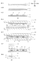
- FIG. 1 shows a cross-sectional view of one embodiment of the phosphor layer sheet of the present invention.
- 2A to 2G are process diagrams of a method of manufacturing a phosphor layer-attached optical semiconductor element using the phosphor layer sheet shown in FIG. 1,
- FIG. 2A is a phosphor layer sheet preparation process
- FIG. FIG. 2C shows a temporary fixing process
- FIG. 2D shows a facing arrangement process
- FIG. 2E shows a stacking process
- FIG. 2F shows a cutting process
- FIG. 2G shows a mounting process.
- 3A to 3B show an embodiment of an optical semiconductor device with a phosphor layer manufactured according to FIG. 2
- FIG. 3A is a plan view
- FIG. 3B is a cross-sectional view taken along line AA in FIG. 3A.
- the vertical direction of the paper is the vertical direction (first direction, thickness direction)
- the upper side of the paper is the upper side (one side in the first direction, the one side in the thickness direction)
- the lower side of the paper is the lower side (the other side in the first direction).
- the other side in the thickness direction The left-right direction on the paper surface is the left-right direction (second direction orthogonal to the first direction, an example of the orthogonal direction to the up-down direction)
- the left side of the paper is the left side (second side in the second direction)
- the right side of the paper is the right side (the other in the second direction).
- Side the vertical direction of the paper is the vertical direction (first direction, thickness direction)
- the upper side of the paper is the upper side (one side in the first direction, the one side in the thickness direction)
- the lower side of the paper is the lower side (the other side in the first direction).
- the other side in the thickness direction The left-right direction on the paper surface is the left-right direction (second direction orthogon
- the paper thickness direction is the front-rear direction (the third direction orthogonal to the first direction and the second direction, an example of the orthogonal direction to the vertical direction), the front side of the paper is the front side (one side in the third direction), and the back side of the paper is the rear side (The other side in the third direction). Specifically, it conforms to the direction arrow in each figure.
- a phosphor layer sheet 1 according to an embodiment of the present invention will be described with reference to FIG.
- the phosphor layer sheet 1 includes a phosphor layer 2 and a white layer 3.
- the phosphor layer sheet 1 is preferably composed of a phosphor layer 2 and a white layer 3.
- the phosphor layer sheet 1 does not include the optical semiconductor element 4 and the diode substrate 15 (electrode substrate; see FIG. 2G for the sign), and is a part of the optical semiconductor element 10 with the phosphor layer and the optical semiconductor device 16, that is, It is a part for producing the optical semiconductor element with a phosphor layer 10 and the optical semiconductor device 16, and is a device that can be distributed industrially and used industrially.
- the phosphor layer sheet 1 includes a phosphor layer 2 and a white layer 3.
- the phosphor layer 2 is a layer containing a phosphor, has a substantially flat plate shape along the left-right direction and the front-rear direction, and has a substantially rectangular shape in plan view.
- the thickness T1 of the phosphor layer 2 is, for example, 30 ⁇ m or more, preferably 50 ⁇ m or more, and, for example, 500 ⁇ m or less, preferably 200 ⁇ m or less.
- the phosphor layer 2 is made of, for example, a sheet-like phosphor-containing cured resin or a phosphor ceramic plate.
- the phosphor-containing cured resin is, for example, a completely cured product (C stage state) of a phosphor resin composition containing a phosphor and a curable resin.
- the phosphor converts the wavelength of light emitted from the optical semiconductor element 4 (described later).
- Examples of the phosphor include a yellow phosphor that can convert blue light into yellow light, and a red phosphor that can convert blue light into red light.
- yellow phosphor examples include silicate phosphors such as (Ba, Sr, Ca) 2 SiO 4 ; Eu, (Sr, Ba) 2 SiO 4 : Eu (barium orthosilicate (BOS)), for example, Y 3 Al Garnet-type phosphors having a garnet-type crystal structure such as 5 O 12 : Ce (YAG (yttrium, aluminum, garnet): Ce), Tb 3 Al 3 O 12 : Ce (TAG (terbium, aluminum, garnet): Ce) Examples thereof include oxynitride phosphors such as Ca- ⁇ -SiAlON.
- silicate phosphors such as (Ba, Sr, Ca) 2 SiO 4 ; Eu, (Sr, Ba) 2 SiO 4 : Eu (barium orthosilicate (BOS)
- Y 3 Al Garnet-type phosphors having a garnet-type crystal structure such as 5 O 12 : Ce (YAG (yttrium, aluminum, garnet): Ce
- red phosphor examples include nitride phosphors such as CaAlSiN 3 : Eu and CaSiN 2 : Eu.
- the phosphor contained in the phosphor-containing cured resin is a particle, and examples of the shape thereof include a spherical shape, a plate shape, and a needle shape.
- the average value of the maximum length of the phosphor (in the case of a sphere, the average particle diameter) is, for example, 0.1 ⁇ m or more, preferably 1 ⁇ m or more, and for example, 200 ⁇ m or less, preferably 100 ⁇ m or less. It is.
- Fluorescent substances can be used alone or in combination of two or more.
- the content ratio of the phosphor is, for example, 10% by mass or more, preferably 20% by mass or more, and, for example, 80% by mass or less, preferably 70% by mass or less with respect to the phosphor resin composition. is there.
- the curable resin is a matrix for uniformly dispersing the phosphor in the phosphor resin composition, and is preferably a transparent resin.
- curable resin examples include silicone resin, epoxy resin, urethane resin, polyimide resin, phenol resin, urea resin, melamine resin, and unsaturated polyester resin.
- thermosetting resins such as a two-stage reaction curable resin and a one-stage reaction curable resin.
- the two-stage reaction curable resin has two reaction mechanisms.
- the A stage state is changed to the B stage (semi-cured), and then in the second stage reaction, the B stage state is obtained.
- C-stage complete curing
- the two-stage reaction curable resin is a thermosetting resin that can be in a B-stage state under appropriate heating conditions.
- the B stage state (semi-cured state) is a state between the A stage state (uncured state) in which the thermosetting resin is liquid and the fully cured C stage state (completely cured state).
- the gelation is slightly progressed, and the compression elastic modulus is a semi-solid state or a solid state smaller than the compression elastic modulus in the C stage state.
- the first stage reaction curable resin has one reaction mechanism, and can be changed from the A stage state to the C stage by the first stage reaction.
- Such a one-stage reaction curable resin can stop the reaction in the middle of the first-stage reaction and change from the A-stage state to the B-stage state.
- the reaction is restarted and includes a thermosetting resin that can be changed from the B-stage state to the C-stage.
- thermosetting resin includes thermosetting resins (two-stage reaction curable resin and one-stage reaction curable resin) that can be in a B-stage state.
- thermosetting resin that can be in the B-stage state
- a silicone resin and an epoxy resin are used, and more preferably, a silicone resin is used.
- silicone resin examples include, for example, a silicone resin having both thermoplasticity and thermosetting properties (thermoplastic / thermosetting silicone resin), no thermoplasticity, and thermosetting properties. Silicone resin (non-thermoplastic / thermosetting silicone resin).
- thermoplastic / thermosetting silicone resin is once plasticized (or liquefied) by heating in the B stage and then cured (C stage) by further heating.
- the thermoplastic / thermosetting silicone resin includes a hot melt type silicone resin.
- a one-step reaction curable resin for example, a phenyl silicone resin described in JP-A-2016-37562.
- the two-stage reaction curable resin include first to sixth thermoplastic / thermosetting silicone resin compositions described in, for example, JP-A-2014-72351 and JP-A-2013-187227. (For example, a composition containing a double-terminal amino type silicone resin, a composition containing a cage-type octasilsesquioxane) and the like.
- the phenyl silicone resin composition has a phenyl group in the main skeleton which is a siloxane bond.
- the phenyl silicone resin composition is preferably an addition reaction curable silicone resin composition. Specifically, it contains an alkenyl group-containing polysiloxane, a hydrosilyl group-containing polysiloxane, and a hydrosilylation catalyst, and at least one of the alkenyl group-containing polysiloxane and the hydrosilyl group-containing polysiloxane has a phenyl group.
- a silicone resin composition etc. are mentioned.
- phenyl silicone resin composition examples include “OE-6630” manufactured by Dow Corning, in addition to the phenyl silicone resin composition described in the above publication.
- non-thermoplastic / thermosetting silicone resin as the two-stage reaction curable resin, for example, the first to eighth condensation / reduction resins described in JP2010-265436A, JP2013-187227A, and the like.
- An addition reaction curable silicone resin composition may be mentioned.
- the same curable resin as that of the white layer 3 is preferably used.
- a thermoplastic / thermosetting silicone resin is preferable, and a phenyl silicone resin composition is more preferable.
- thermosetting silicone resins that do not take the B stage state include methyl silicone resins such as ELASTOSIL series (manufactured by Asahi Kasei Wacker Silicone, specifically ELASTOSIL LR7665) and KER series (manufactured by Shin-Etsu Silicone). Examples thereof include a composition.
- the curable resin can be used alone or in combination of two or more.
- the content of the curable resin is the balance of the content of the phosphor (and additive), and is, for example, 20% by mass or more, preferably 30% by mass or more, with respect to the phosphor resin composition. For example, it is 90 mass% or less, Preferably, it is 80 mass% or less.
- the phosphor resin composition may contain a known additive such as inorganic particles in an appropriate ratio.
- inorganic particles examples include light diffusing inorganic particles described later in the white resin composition, preferably silica particles and glass particles, and more preferably glass particles.
- the content ratio is, for example, 1% by mass or more, preferably 5% by mass or more, more preferably 10% by mass or more, with respect to the phosphor resin composition.
- it is 70 mass% or less, Preferably, it is 50 mass% or less, More preferably, it is 30 mass% or less.
- the phosphor ceramic plate can be obtained by using the above phosphor as a ceramic material and sintering the above ceramic material. Alternatively, it can also be obtained by sintering the above-described phosphor raw material and performing a chemical reaction by sintering.
- the white layer 3 is a white reflective layer that can reflect the light emitted from the optical semiconductor element 4.
- the white layer 3 is disposed on the upper surface of the phosphor layer 2 so that the entire lower surface of the white layer 3 is in contact with the entire upper surface of the phosphor layer 2.
- the white layer 3 has a substantially flat plate shape along the left-right direction and the front-rear direction, and has a substantially rectangular shape in plan view.
- the thickness T2 of the white layer 3 is, for example, 50 ⁇ m or more, preferably 100 ⁇ m or more, and for example, 600 ⁇ m or less, preferably 400 ⁇ m or less.
- the ratio (T2 / T1) of the thickness T2 of the white layer 3 to the thickness T1 of the phosphor layer 2 is, for example, 1 or more, preferably 2 or more, and for example, 10 or less, preferably 8 or less. is there.
- the white layer 3 is in a semi-cured state (B stage state) and has both thermoplasticity and thermosetting properties. That is, the white layer 3 is once plasticized or liquefied by heating and then cured (C stage) by further heating.
- the white layer 3 is formed from a white resin and a white resin composition containing a thermoplastic / thermosetting silicone resin composition.
- the white layer 3 is formed from a white resin composition comprising white particles and a thermoplastic / thermosetting silicone resin composition.
- white particles examples include white inorganic particles and white organic particles.
- white inorganic particles are used from the viewpoint of heat dissipation and durability.
- Examples of the material constituting the white inorganic particles include oxides such as titanium oxide, zinc oxide, zirconium oxide, and aluminum oxide, such as carbonates such as lead white (basic lead carbonate) and calcium carbonate, such as kaolin. Clay minerals. From the viewpoints of brightness and heat dissipation, an oxide is preferable, and titanium oxide is more preferable.
- the average particle diameter of the white particles is, for example, 0.1 ⁇ m or more, preferably 0.2 ⁇ m or more, and for example, 2.0 ⁇ m or less, preferably 0.5 ⁇ m or less.
- the average particle diameter of the particles is calculated as a D50 value, and specifically measured by a laser diffraction particle size distribution meter.
- the content ratio of the white particles is, for example, 3% by mass or more, preferably 5% by mass or more, more preferably 10% by mass or more, and, for example, 70% by mass or less with respect to the white resin composition. Preferably, it is 50 mass% or less, More preferably, it is 40 mass% or less.
- thermoplastic / thermosetting silicone resin composition is a matrix in which white particles are uniformly dispersed in the white resin composition, and is preferably a transparent resin.
- thermoplastic / thermosetting silicone resin composition examples include those similar to the thermoplastic / thermosetting silicone resin composition described above for the phosphor layer 2.
- a one-step reaction curable resin is mentioned, More preferably, a phenyl-type silicone resin composition is mentioned.
- the phenyl silicone resin composition has a phenyl group in the main skeleton that is a siloxane bond, and preferably includes an addition reaction curable silicone.
- Specific examples of the phenyl silicone resin composition include a phenyl silicone resin composition described in JP-A-2016-37562, “OE-6630” manufactured by Dow Corning, and the like.
- the thickness of the white film 5 formed between the phosphor layer 2 and the optical semiconductor element 4 can be reduced in the method for manufacturing the layered element 10 described later. It can be adjusted easily and a thin and uniform white film 5 can be formed.
- the content ratio of the thermoplastic / thermosetting silicone resin composition is the balance of the content ratio of the white particles (and additives described later), and is, for example, 30% by mass or more, preferably with respect to the white resin composition. Is 50% by mass or more, more preferably 60% by mass or more, and for example, 97% by mass or less, preferably 95% by mass or less, more preferably 90% by mass or less.
- the white resin composition can contain particles other than white particles.
- Examples of such particles include light diffusing inorganic particles.
- Examples of the light diffusing inorganic particles include silica particles and composite inorganic oxide particles (such as glass particles).
- the composite inorganic oxide particles contain, for example, silica or silica and boron oxide as main components, and also include aluminum oxide, calcium oxide, zinc oxide, strontium oxide, magnesium oxide, zirconium oxide, barium oxide, antimony oxide, and the like. Is contained as a minor component.
- the content ratio of the main component in the composite inorganic oxide particles is, for example, 40% by mass or more, preferably 50% by mass or more, and for example, 90% by mass or less, preferably with respect to the composite inorganic oxide particles. 80% by mass or less.
- the content ratio of the subcomponent is the remainder of the content ratio of the main component described above.
- the light diffusing inorganic particles are preferably silica particles from the viewpoint of heat dissipation and brightness.
- the average particle size of the light diffusing inorganic particles is preferably larger than the average particle size of the white particles, specifically, for example, 1.0 ⁇ m or more, preferably 2.0 ⁇ m or more. It is 10 ⁇ m or less, preferably 5.0 ⁇ m or less, and more preferably 3.0 ⁇ m or less.
- the content ratio of the light diffusing inorganic particles is, for example, 1% by mass or more, preferably 5% by mass or more, more preferably 10% by mass or more with respect to the white resin composition. It is 70 mass% or less, Preferably, it is 50 mass% or less, More preferably, it is 30 mass% or less.
- the heat dissipation can be improved while reducing the resin content.
- the particles are preferably composed only of white particles from the viewpoint of heat dissipation, that is, do not contain particles other than white particles. It is preferable.
- the white resin composition may contain a known additive in an appropriate ratio.
- the phosphor layer sheet 1 can be manufactured, for example, by first forming the phosphor layer 2 and then laminating the white layer 3 on the upper surface of the phosphor layer 2.
- the phosphor layer 2 is made of a phosphor-containing curable resin
- a varnish of a phosphor resin composition containing the phosphor and a curable resin (A stage) is prepared.
- the varnish of the phosphor resin composition is applied to the upper surface of the release sheet.
- the phosphor resin composition is C-staged (completely cured).
- the curable resin is a thermosetting resin
- the phosphor resin composition is heated.
- the heating temperature is, for example, 100 ° C. or higher, preferably 120 ° C. or higher, and for example, 200 ° C. or lower, preferably 160 ° C. or lower.
- the heating time is, for example, 5 minutes or more, preferably 10 minutes or more, and for example, 60 minutes or less, preferably 30 minutes or less.
- the phosphor layer 2 is a phosphor ceramic plate
- a green sheet is formed by applying and drying a slurry containing a phosphor material, a binder resin, and a solvent on the upper surface of the release sheet. The sheet is fired.
- JP-A-2015-216355 can be referred to for the slurry material and firing conditions.
- the tensile elastic modulus E at 25 ° C. of the obtained phosphor layer 2 is, for example, 1 MPa or more, preferably 3 MPa or more, more preferably 10 MPa or more, and for example, 150 MPa or less, preferably 100 MPa or less. Preferably, it is 50 MPa or less.
- the phosphor layer 2 can be made to have high hardness and low brittleness. Therefore, in the laminating process described later, the white resin composition between the phosphor layer 2 and the light emitting surface 21 of the optical semiconductor element 4 can be surely compressed in the vertical direction and stretched in the surface direction.
- the white film 5 can be formed uniformly. Further, since the shape of the formed white film 5 is uniform and stable, the brightness of the layered element 10 can be improved.
- the tensile elastic modulus E is obtained by measuring the phosphor layer 2 under the condition of a tensile speed of 300 mm / min.
- a white resin and a white resin composition varnish containing a thermoplastic / thermosetting silicone resin composition are prepared. Subsequently, the varnish of the white resin composition is applied to the upper surface of the phosphor layer 2.
- Application method is not limited, and examples thereof include a method using an applicator, potting, cast coating, spin coating, and roll coating.
- the white resin composition is B-staged. Specifically, the white resin composition is heated.
- the heating conditions are appropriately set according to the composition of the white resin composition and the intended melt viscosity of the white resin composition as long as the white resin composition is B-staged but not C-staged.
- the heating temperature is, for example, 50 ° C. or more, preferably 60 ° C. or more, and for example, 120 ° C. or less, preferably 100 ° C. or less.
- the heating time is, for example, 3 minutes or more, preferably 5 minutes or more, and for example, 120 minutes or less, preferably 60 minutes or less.
- the resulting B-stage white layer 3 has a melt viscosity at 60 ° C. of, for example, 5 Pa ⁇ s or more, preferably 10 Pa ⁇ s or more, more preferably 15 Pa ⁇ s or more, and for example, 800 Pa ⁇ s. Hereinafter, it is preferably 600 Pa ⁇ s or less, more preferably 550 Pa ⁇ s or less.
- the melt viscosity of the white layer 3 in the above range, the handling property of the white layer 3 can be improved and good moldability can be obtained. Further, it is possible to easily adjust the film thickness of the white film 5 formed on the layered element 10 and to form the white film 5 thinner. Furthermore, the brightness of the layered element 10 can be improved.
- the melt viscosity is obtained by adjusting the temperature of the white layer 3 of the B stage to 60 ° C. and measuring using an E-type cone.
- the rotation speed is selected so that the torque is in the range of 30 to 90%, for example.
- the viscosity after the white layer 3 is uniformly heated to 60 ° C. and the measured viscosity becomes constant, specifically, the value after 3 minutes from the start of measurement is employed.
- the phosphor layer sheet 1 thus obtained can be used as, for example, a sealing sheet for manufacturing the layered element 10 and the optical semiconductor device 16 described later.
- the upper surface or the lower surface of the phosphor layer sheet 1 shown in FIG. 1 is exposed.
- a release sheet can be provided on the upper surface and / or the lower surface of the phosphor layer sheet 1.
- the manufacturing method of the optical semiconductor element 10 with a phosphor layer includes, for example, a phosphor layer sheet preparation process, a temporary fixing sheet preparation process, a temporary fixing process, an opposing arrangement process, a lamination process, A C-staging process and a cutting process are provided.
- the phosphor layer sheet 1 is prepared by the manufacturing method described above.
- the temporarily fixing sheet 11 is disposed on the upper surface of the carrier 12.
- the temporary fixing sheet 11 is, for example, a sheet having pressure-sensitive adhesiveness on both sides.
- the temporary fixing sheet 11 may have, for example, a single-layer structure formed from a single pressure-sensitive adhesive layer, and the pressure-sensitive adhesive layer is laminated on both surfaces of the support substrate. You may have a multilayer structure.
- the pressure-sensitive adhesive layer is formed of a pressure-sensitive adhesive whose pressure-sensitive adhesive force is reduced by, for example, treatment (for example, irradiation of ultraviolet rays or heating).
- the carrier 12 is a support plate for supporting the temporarily fixed sheet 11 from below, and is made of, for example, a hard material.
- the hard material include glass, ceramic, and stainless steel.
- a plurality of optical semiconductor elements 4 (described later) are temporarily fixed on the temporary fixing sheet 11.
- the electrodes 24 of the plurality of optical semiconductor elements 4 are pressure-bonded to the upper surface of the temporary fixing sheet 42.
- the plurality of optical semiconductor elements 4 are aligned and arranged on the temporary fixing sheet at intervals in the left-right direction and the front-rear direction.
- an element arrangement carrier 13 including the carrier 12, the temporary fixing sheet 11 arranged on the upper side of the carrier 12, and the plurality of optical semiconductor elements 4 arranged in alignment on the temporary fixing sheet 11 is obtained.
- the element arrangement carrier 13 and the phosphor layer sheet 1 are arranged to face each other with an interval in the vertical direction.
- the element arrangement carrier 13 and the phosphor layer sheet 1 are set in the press machine 30.
- the press machine 30 is a heat press machine provided with a heat source, and is provided with a lower plate 31, an upper plate 32 that is arranged on the upper side of the lower plate 31 and configured to be movable downward with respect to the lower plate 31, A spacer 33 is mounted on the upper surface of the plate 31 and adjusts the distance between the upper plate 32 and the lower plate 31 during hot pressing.
- the phosphor layer sheet 1 is arranged on the upper surface of the lower plate 31 so that the white layer 3 is on the upper side.
- the element arrangement carrier 13 is fixed to the lower surface of the upper plate 32 so that the optical semiconductor element 4 is on the lower side.
- the spacer 33 is arranged so that the light emitting surface 21 of the optical semiconductor element 4 reaches the white layer side surface of the phosphor layer 2 during hot pressing, that is, the light emitting surface 21 is formed between the phosphor layer 2 and the white layer 3. Adjust to reach near the interface.
- the phosphor layer sheet 1 is laminated on the element arrangement carrier 13 in the lamination step.
- hot pressing is performed by moving the upper plate 32 downward while operating the heat source of the press machine 30.
- the optical semiconductor element 4 is buried in the white layer 3, and the light emitting surface 21 of the optical semiconductor element 4 is located near the white layer side surface (upper surface) of the phosphor layer 2.
- the white layer 3 has a thermoplastic and thermosetting silicone resin composition and is in a semi-cured state, the white layer 3 is easily melted by heat, and the light emitting surface 21 and the phosphor layer 2 It is formed so as to spread uniformly and thinly in a slight gap (interface) with the surface of the white layer side. Thereafter, the white film 5 having a desired thickness can be formed by a thermosetting reaction.
- the pressure of the hot press is, for example, 0.01 MPa or more, preferably 0.1 MPa or more, and for example, 10 MPa or less, preferably 5 MPa or less.
- the temperature of the hot press may be a temperature at which the white layer 3 is melted, for example, 40 ° C or higher, preferably 45 ° C or higher, more preferably 50 ° C or higher, and for example, 180 ° C or lower, preferably Is 150 ° C. or less, more preferably less than 100 ° C.
- the time of the heating press is, for example, 1 second or more, preferably 3 seconds or more, and for example, 30 minutes or less, preferably 10 minutes or less.
- the layered element assembly 14 including the plurality of optical semiconductor elements 4, the white layer 3, and the phosphor layer 2 is obtained in a state of being temporarily fixed to the temporary fixing sheet 11.
- the white layer 3 in the B-stage state (semi-cured state) is converted to the C-stage.
- a heating process is performed. That is, the layered element assembly 14 is removed from the press machine 30 and heated by an oven or the like.
- the heating temperature is, for example, 100 ° C. or more, preferably 120 ° C. or more, more preferably 130 ° C. or more, and for example, 200 ° C. or less, preferably 160 ° C. or less, more preferably 150 ° C. or less. is there.
- the heating time is, for example, 10 minutes or more, preferably 30 minutes or more, more preferably 60 minutes or more, and for example, 480 minutes or less, preferably 300 minutes or less, more preferably 180 minutes. It is as follows. Note that the heating can be performed a plurality of times at different temperatures.
- the layered element assembly 14 is cut.
- the white layer 3 and the phosphor layer 2 between the adjacent optical semiconductor elements 4 are cut by dicing or the like. As a result, the layered element assembly 14 is singulated.
- the layered element 10 including one optical semiconductor element 4, the white layer 3, and the phosphor layer 2 is obtained in a state of being temporarily fixed to the temporary fixing sheet 11.
- the layered element 10 is peeled off from the temporarily fixed sheet 11 as indicated by a virtual line in FIG. 2F.
- the white layer 3 covering the facing surface 22 is grinded so that the facing surface 22 (electrode) is exposed.
- the layered element 10 including one optical semiconductor element 4, the white layer 3, and the phosphor layer 2 is obtained.
- an optical semiconductor device 16 such as a light emitting diode device can be obtained by flip-chip mounting the layered element 10 on an electrode substrate such as a diode substrate 15 (mounting process).
- the diode substrate 15 has a substantially flat plate shape. Specifically, the diode substrate 15 is formed of a laminated plate in which a conductor layer is laminated as a circuit pattern on the upper surface of an insulating substrate.
- the insulating substrate is made of, for example, a silicon substrate, a ceramic substrate, a plastic substrate (for example, a polyimide resin substrate), or the like.
- the conductor layer is made of a conductor such as gold, copper, silver, or nickel.
- the conductor layer includes an electrode (not shown) for electrical connection with a single optical semiconductor element 4.
- the thickness of the diode substrate 15 is, for example, 25 ⁇ m or more, preferably 50 ⁇ m or more, and, for example, 2000 ⁇ m or less, preferably 1000 ⁇ m or less.
- the layered element 10 obtained by the above manufacturing method includes the optical semiconductor element 4, the white layer 3, and the phosphor layer 2.
- the optical semiconductor element 4 is, for example, an LED (light emitting diode element) or an LD (semiconductor laser element) that converts electrical energy into optical energy.
- the optical semiconductor element 4 is a blue LED that emits blue light.
- the optical semiconductor element 4 does not include a rectifier (semiconductor element) such as a transistor having a technical field different from that of the optical semiconductor element.
- the optical semiconductor element 4 has a substantially flat plate shape along the left-right direction and the front-rear direction.
- the optical semiconductor element 4 has a substantially rectangular shape in plan view (preferably, a substantially square shape in plan view).
- the optical semiconductor element 4 includes a light emitting surface 21, a facing surface 22, and a side surface 23.
- the light emitting surface 21 is the upper surface of the optical semiconductor element 4.
- the light emitting surface 21 has a flat shape.
- a white film 5 (described later) is provided on the light emitting surface 21.
- the facing surface 22 is a lower surface of the optical semiconductor element 4 and is a surface on which the electrode 24 is provided.
- the facing surface 22 is disposed to face the light emitting surface 21 with a space on the lower side.
- a plurality (two) of the electrodes 24 are provided and have a shape that slightly protrudes downward from the facing surface 22.
- the side surface 23 connects the peripheral edge of the light emitting surface 21 and the peripheral edge of the facing surface 22.
- the thickness T3 (length in the vertical direction) is, for example, 0.1 ⁇ m or more, preferably 1 ⁇ m or more, more preferably 10 ⁇ m or more. For example, it is 500 micrometers or less, Preferably, it is 200 micrometers or less.
- the length in the left-right direction and / or the front-rear direction of the optical semiconductor element 4 is, for example, 200 ⁇ m or more, preferably 500 ⁇ m or more, and for example, 3000 ⁇ m or less, preferably 2000 ⁇ m or less.
- the white layer 3 in the layered element 10 is in contact with and covers the light emitting surface 21 and the side surface 23 of the optical semiconductor element. Further, the white layer 3 is disposed below the phosphor layer 2. Specifically, the white layer 3 is in contact with and covers the lower surface of the phosphor layer 2.
- the white layer 3 is integrally provided with a white film 5 and a white side portion 6.
- the white film 5 is disposed above the light emitting surface 21 of the optical semiconductor element 4. Specifically, the white film 5 is light-transmitted so that the entire lower surface thereof is in contact with the entire upper surface of the entire light emitting surface 21 and the entire upper surface thereof is in contact with a part (center) of the lower surface of the phosphor layer 2. Arranged between the semiconductor element 4 and the phosphor layer 2.
- the white film 5 has a substantially flat plate shape along the left-right direction and the front-rear direction, and has a substantially rectangular shape in plan view (preferably, a substantially square shape in plan view).
- the white film 5 is formed so as to coincide with the light emitting surface 21 when projected in the thickness direction.
- the thickness T4 of the white film 5 is, for example, 1 ⁇ m or more, preferably 2 ⁇ m or more, more preferably 4 ⁇ m or more, for example, 20 ⁇ m or less, preferably from the viewpoint of brightness, heat dissipation, and bonding reliability. , 13 ⁇ m or less, more preferably 7 ⁇ m or less.
- the ratio (T4 / T3) of the thickness T4 of the white film 5 to the thickness T3 of the optical semiconductor element 4 is, for example, 0.001 or more, preferably 0.005 or more, and, for example, 0.200 or less, Preferably, it is 0.100 or less.
- the white side portion 6 is disposed on the side of the white film 5 and the optical semiconductor element 4 (periphery, that is, outside in the left-right direction and outside in the front-rear direction). Specifically, the white side portion 6 is arranged so as to be continuous with the entire peripheral end surface of the white film 5 and to be in contact with the entire side surface 23 of the optical semiconductor element 4.
- the white side portion 6 has a substantially rectangular frame shape in plan view.
- the white side portion 6 is formed so that its inner shape matches the shape of the optical semiconductor element 4 and its outer shape matches the shape of the phosphor layer 2 when projected in the thickness direction.
- the thickness of the white side portion 6 is the same as the sum of the thickness T3 of the optical semiconductor element 4 and the thickness T4 of the white film 5.
- the white layer 3 is formed from a white resin composition containing white particles and a thermoplastic / thermosetting silicone resin composition. More specifically, the white layer 3 is a completely cured body (C Stage state).
- the white layer 3 has a reflectance of 70% or more, preferably 80% or more, more preferably 90% or more, for example, 100% when irradiated with light having a wavelength of 450 nm with a thickness of 100 ⁇ m. It is as follows. By setting the reflectance within the above range, the light extraction efficiency can be improved.
- the method for measuring the reflectance can be obtained by measuring the reflectance at a wavelength of 450 nm using an ultraviolet-visible near-infrared spectrophotometer with an optical path confirmation method using an integrating sphere.
- the phosphor layer 2 is disposed on the upper side of the white film 5. Specifically, the phosphor layer 2 is disposed on the upper surface of the white layer 3 such that the entire lower surface of the phosphor layer 2 is in contact with the entire upper surface of the white layer 3 (white film 5 and white side portion 6). Yes.
- the phosphor layer 2 has a substantially flat plate shape along the left-right direction and the front-rear direction, and has a substantially rectangular shape in plan view (preferably, a substantially square shape in plan view).
- the phosphor layer 2 is formed so as to coincide with the white layer 3 when projected in the vertical direction. That is, the peripheral side surface of the phosphor layer 2 is flush with the peripheral side surface of the white side portion 6.
- the ratio (T4 / T1) of the thickness T4 of the white film 5 to the thickness T1 of the phosphor layer 2 is, for example, 0.001 or more, preferably 0.005 or more, and, for example, 0.3 or less, Preferably, it is 0.2 or less.
- the phosphor layer 2 is made of a sheet-like phosphor-containing curable resin or a phosphor ceramic plate.
- the layered element 10 is not the optical semiconductor device 16, that is, does not include an electrode substrate such as the diode substrate 15 provided in the optical semiconductor device 16.
- the layered element 10 includes an optical semiconductor element 4, a white layer 3, and a phosphor layer 2.
- the layered element 10 is preferably composed of the optical semiconductor element 4, the white layer 3, and the phosphor layer 2. That is, the layered element 10 is configured so that it is not yet electrically connected to the electrode provided on the diode substrate 15 of the optical semiconductor device 16.
- the layered element 10 is a component for manufacturing the optical semiconductor device 16, that is, a component for manufacturing the optical semiconductor device 16, and is a device that can be distributed and used industrially.
- the layered element 10 can be manufactured by a simple process. That is, the layered element 10 can be manufactured by performing the above-described laminating process (hot pressing) once. Therefore, the number of manufacturing processes can be reduced.
- a white film 5 serving as an adhesive can be disposed between the phosphor layer 2 and the optical semiconductor element 4. Therefore, in the layered element 10, the phosphor layer 2 and the optical semiconductor element 4. The joint reliability can be improved.
- the thickness of the white film 5 existing between the phosphor layer 2 and the optical semiconductor element 4 can be easily adjusted by adjusting the spacer 33.
- the white layer 3 of the phosphor layer sheet 1 is disposed between the upper surface of the phosphor layer 2 having high hardness and low brittleness (the surface on the white layer 3 side) and the light emitting surface 21 of the optical semiconductor element 4 in the laminating step.
- the thin white film 5 can be formed on the layered element 10. Therefore, reflection and absorption of light entering the phosphor layer 2 from the light emitting surface 21 can be reduced. Therefore, it is possible to suppress a reduction in brightness while improving the bonding reliability.
- the heat generated in the phosphor layer 2 can be dissipated through the white film 5, so that the heat dissipation is excellent.
- a white side portion 6 disposed around the optical semiconductor element 4 can be further disposed. Therefore, the light emitted from the side of the optical semiconductor element 4 can be reflected, and the brightness can be improved.
- a phenyl-based silicone resin composition (one-stage reaction curable resin that can be in a B-stage state, thermoplastic / thermosetting silicone) Resin, addition reaction curing type) was prepared.
- a phosphor resin composition A was prepared by mixing 100 parts by mass of this phenyl silicone resin composition with 40 parts by mass of a yellow phosphor (“Y-468”, manufactured by Nemoto Special Chemical Co., Ltd.).
- a phenyl silicone resin composition was prepared in accordance with Preparation Example 1 described in Examples of JP-A-2016-37562.
- a phosphor resin composition B was prepared by mixing 100 parts by mass of this phenyl silicone resin composition with 40 parts by mass of a yellow phosphor (as described above) and 50 parts by mass of glass particles.
- Phosphor resin composition C was prepared by mixing 40 parts by mass of a yellow phosphor (as described above) with 100 parts by mass of a methyl silicone resin composition (“KER-2500, manufactured by Shin-Etsu Chemical Co., Ltd., addition reaction curing type)”. Was prepared.
- White resin composition A was prepared by mixing 30 parts by mass of titanium oxide (white particles, “R706S”, DuPont, average particle size 0.36 ⁇ m) with 100 parts by mass of the phenyl-based silicone resin composition.
- a white resin composition B was prepared by mixing parts by mass.
- phenyl silicone resin composition 100 parts by mass of phenyl silicone resin composition, 30 parts by mass of titanium oxide (same as above) and 10 parts by mass of silica (light diffusing inorganic particles, “FB-3SDC”, manufactured by DENKA, average particle diameter 3.4 ⁇ m) Were mixed to prepare a white resin composition C.
- Example 1 First, the phosphor resin composition A was applied on a release sheet and heated at 120 ° C. for 10 minutes to form a C-stage phosphor layer (thickness: 100 ⁇ m). The elastic modulus E of the phosphor layer was 37 MPa. Subsequently, the white resin composition A was apply
- a plurality of optical semiconductor elements (1.0 mm square, thickness 150 ⁇ m, trade name “EDI-FA4545A”, manufactured by Epistar Co., Ltd.) with electrodes provided on the opposing surface are prepared, and the optical semiconductor elements are placed on the temporary fixing sheet.
- a pitch of 1.64 mm 20 in the front-rear direction and 20 in the left-right direction were aligned (see FIG. 2C). Thereby, an element arrangement carrier was obtained.
- the phosphor layer sheet and the element arrangement carrier were set in a press machine (see FIG. 2D). Specifically, the phosphor layer sheet is arranged on the upper surface of the lower plate of the press machine so that the white layer is on the upper side, the element arrangement carrier is arranged on the lower surface of the upper plate of the press machine, and the optical semiconductor element is It was fixed to be on the lower side. In addition, the spacers were adjusted so that the height of the interface between the phosphor layer and the white layer was close to the position during pressing.
- the layered element assembly was allowed to stand in an oven at 150 ° C. for 120 minutes, so that the white layer was converted to the C stage.
- the white layer and the phosphor layer between the adjacent optical semiconductor elements were cut by dicing to separate the layered element assembly. Subsequently, the separated layered element was peeled off from the temporarily fixed sheet, and then the white layer covering the opposing surface was ground so that the opposing surface was exposed (see FIG. 2F).
- Examples 2 to 7 A phosphor layer sheet and a layered element were produced in the same manner as in Example 1 except that the curing conditions of the white resin composition A were adjusted and the melt viscosity of the white layer was changed to the melt viscosity shown in Table 1.
- Example 8 A phosphor layer sheet and a layered element were produced in the same manner as in Example 1 except that the white resin composition B was used instead of the white resin composition A.
- Example 9 A phosphor layer sheet and a layered element were produced in the same manner as in Example 1 except that the white resin composition C was used instead of the white resin composition A.
- Example 10 Phosphor layer sheet as in Example 1, except that the phosphor resin composition B is used in place of the phosphor resin composition A, and the melt viscosity of the white layer is changed to the melt viscosity shown in Table 1. And layered elements were manufactured.
- Example 11 A phosphor layer sheet and a layered element were produced in the same manner as in Example 1 except that the phosphor resin composition C was used instead of the phosphor resin composition A.
- Example 1 Example except that the white resin composition D was used in place of the white resin composition A, the curing conditions of the white resin composition D were adjusted, and the melt viscosity of the white layer was changed to the melt viscosity described in Table 1. In the same manner as in Example 1, a phosphor layer sheet was produced.
- Example 2 a spacer was adjusted in the same manner as in Example 1, and an element with a thin white film (thickness 1 to 20 ⁇ m) was attempted to be manufactured.
- a layered element having a white film thickness of 22 ⁇ m was manufactured because the white layer did not melt and did not spread uniformly and wet during hot pressing.
- Comparative Example 2 A phosphor layer sheet was produced in the same manner as in Comparative Example 1 except that the curing conditions of the white resin composition D were adjusted and the melt viscosity of the white layer was changed to the melt viscosity shown in Table 1.
- FIGS. 2B and 2C A layered element that does not form a white film was produced. That is, a layered element in which the light emitting surface of the optical semiconductor element and the phosphor layer are in direct contact was produced. Specifically, the temporary fixing sheet preparation step and the temporary fixing step shown in FIGS. 2B and 2C were performed to obtain an element arrangement carrier. Next, the white resin composition A of A stage is placed on the upper surface of the lower plate, the device placement carrier is placed on the lower surface of the upper plate, and hot-pressed, and the light emitting surface and the side surface of the optical semiconductor device of the device placement carrier are white Coated with a layer. Next, the white layer covering the light emitting surface of the optical semiconductor element was removed to expose the light emitting surface. Next, a phosphor layer having the phosphor composition A as a C stage was prepared, and this was hot-pressed on the light emitting surface.
- the brightness of each optical semiconductor device was determined with the brightness (millilumen) of the optical semiconductor device of Example 1 as 100%. The results are shown in Table 1.
- the phosphor layer sheet and phosphor layer-attached optical semiconductor element of the present invention can be applied to various industrial products, and can be suitably used for light emitting devices such as white light emitting devices.
Landscapes
- Physics & Mathematics (AREA)
- General Physics & Mathematics (AREA)
- Optics & Photonics (AREA)
- Led Device Packages (AREA)
- Optical Filters (AREA)
Abstract
Cette feuille de couche de phosphore est pourvue d'une couche de phosphore et d'une couche blanche disposée sur un côté de la couche de phosphore dans la direction de l'épaisseur. La couche de phosphore est une résine durcie contenant du phosphore, ou une plaque de phosphore céramique, et la couche blanche est à l'état semi-durci et contient des particules blanches et une composition de résine de silicone ayant à la fois des propriétés thermoplastiques et thermodurcissables.
Applications Claiming Priority (2)
| Application Number | Priority Date | Filing Date | Title |
|---|---|---|---|
| JP2016123854A JP2017227772A (ja) | 2016-06-22 | 2016-06-22 | 蛍光体層シート、および、蛍光体層付光半導体素子の製造方法 |
| JP2016-123854 | 2016-06-22 |
Publications (1)
| Publication Number | Publication Date |
|---|---|
| WO2017221608A1 true WO2017221608A1 (fr) | 2017-12-28 |
Family
ID=60784186
Family Applications (1)
| Application Number | Title | Priority Date | Filing Date |
|---|---|---|---|
| PCT/JP2017/019061 Ceased WO2017221608A1 (fr) | 2016-06-22 | 2017-05-22 | Feuille de couche de phosphore et procédé de fabrication d'un élément de semi-conducteur optique avec une couche de phosphore |
Country Status (2)
| Country | Link |
|---|---|
| JP (1) | JP2017227772A (fr) |
| WO (1) | WO2017221608A1 (fr) |
Cited By (2)
| Publication number | Priority date | Publication date | Assignee | Title |
|---|---|---|---|---|
| JP2019145739A (ja) * | 2018-02-23 | 2019-08-29 | 株式会社朝日ラバー | 光拡散膜付led発光装置、光拡散膜形成用インク及びled発光装置用光拡散シート |
| CN110183979A (zh) * | 2019-06-24 | 2019-08-30 | 弗洛里光电材料(苏州)有限公司 | 多层复合膜及其应用 |
Citations (6)
| Publication number | Priority date | Publication date | Assignee | Title |
|---|---|---|---|---|
| WO2007007582A1 (fr) * | 2005-07-08 | 2007-01-18 | Kabushiki Kaisha Toshiba | Rétroéclairage et affichage à cristaux liquides l’utilisant |
| WO2012090702A1 (fr) * | 2010-12-28 | 2012-07-05 | 株式会社日立製作所 | Dispositif d'éclairage |
| JP2013187227A (ja) * | 2012-03-06 | 2013-09-19 | Nitto Denko Corp | 封止シート、発光ダイオード装置およびその製造方法 |
| JP2013258209A (ja) * | 2012-06-11 | 2013-12-26 | Nitto Denko Corp | 封止シート、発光ダイオード装置およびその製造方法 |
| JP2014072351A (ja) * | 2012-09-28 | 2014-04-21 | Nitto Denko Corp | 蛍光体層貼着キット、光半導体素子−蛍光体層貼着体および光半導体装置 |
| JP2016213451A (ja) * | 2015-05-01 | 2016-12-15 | 日東電工株式会社 | 蛍光体層−封止層付光半導体素子の製造方法 |
-
2016
- 2016-06-22 JP JP2016123854A patent/JP2017227772A/ja active Pending
-
2017
- 2017-05-22 WO PCT/JP2017/019061 patent/WO2017221608A1/fr not_active Ceased
Patent Citations (6)
| Publication number | Priority date | Publication date | Assignee | Title |
|---|---|---|---|---|
| WO2007007582A1 (fr) * | 2005-07-08 | 2007-01-18 | Kabushiki Kaisha Toshiba | Rétroéclairage et affichage à cristaux liquides l’utilisant |
| WO2012090702A1 (fr) * | 2010-12-28 | 2012-07-05 | 株式会社日立製作所 | Dispositif d'éclairage |
| JP2013187227A (ja) * | 2012-03-06 | 2013-09-19 | Nitto Denko Corp | 封止シート、発光ダイオード装置およびその製造方法 |
| JP2013258209A (ja) * | 2012-06-11 | 2013-12-26 | Nitto Denko Corp | 封止シート、発光ダイオード装置およびその製造方法 |
| JP2014072351A (ja) * | 2012-09-28 | 2014-04-21 | Nitto Denko Corp | 蛍光体層貼着キット、光半導体素子−蛍光体層貼着体および光半導体装置 |
| JP2016213451A (ja) * | 2015-05-01 | 2016-12-15 | 日東電工株式会社 | 蛍光体層−封止層付光半導体素子の製造方法 |
Cited By (3)
| Publication number | Priority date | Publication date | Assignee | Title |
|---|---|---|---|---|
| JP2019145739A (ja) * | 2018-02-23 | 2019-08-29 | 株式会社朝日ラバー | 光拡散膜付led発光装置、光拡散膜形成用インク及びled発光装置用光拡散シート |
| CN110183979A (zh) * | 2019-06-24 | 2019-08-30 | 弗洛里光电材料(苏州)有限公司 | 多层复合膜及其应用 |
| CN110183979B (zh) * | 2019-06-24 | 2024-05-14 | 江苏穿越光电科技有限公司 | 多层复合膜及其应用 |
Also Published As
| Publication number | Publication date |
|---|---|
| JP2017227772A (ja) | 2017-12-28 |
Similar Documents
| Publication | Publication Date | Title |
|---|---|---|
| TWI749058B (zh) | 光學半導體元件覆蓋用薄片 | |
| JP6519311B2 (ja) | 発光装置 | |
| JP5960014B2 (ja) | 蛍光接着シート、光半導体素子−蛍光体層感圧接着体および光半導体装置 | |
| KR102541533B1 (ko) | 광 반사층 부착 광 반도체 소자, 및 광 반사층 및 형광체층 부착 광 반도체 소자의 제조 방법 | |
| JP5862066B2 (ja) | 蛍光体含有シート、それを用いたled発光装置およびその製造方法 | |
| JP2014096491A (ja) | 蛍光体層被覆半導体素子、その製造方法、半導体装置およびその製造方法 | |
| KR20120117661A (ko) | 반사 수지 시트, 발광 다이오드 장치 및 그 제조 방법 | |
| JP2014168036A (ja) | 封止層被覆半導体素子、その製造方法および半導体装置 | |
| WO2014014008A1 (fr) | Procédé de production d'un élément semi-conducteur revêtu d'une couche de scellement, et dispositif semi-conducteur | |
| JP2014116587A (ja) | 蛍光体含有樹脂シート、これを用いたled素子およびその製造方法 | |
| US20170030556A1 (en) | Wavelength conversion member and production method thereof | |
| JP2016119454A (ja) | 蛍光体層被覆光半導体素子およびその製造方法 | |
| WO2017221606A1 (fr) | Élément semi-conducteur optique ayant une couche de phosphore, et procédé de fabrication d'un élément semi-conducteur optique | |
| JP2016213451A (ja) | 蛍光体層−封止層付光半導体素子の製造方法 | |
| US20170040502A1 (en) | Wavelength conversion bonding member, wavelength conversion heat dissipation member, and light-emitting device | |
| WO2017221607A1 (fr) | Dispositif à semi-conducteur optique avec couche de phosphore | |
| JP2013138106A (ja) | 封止シート、光半導体装置の製造方法、光半導体装置および照明装置 | |
| JP2018041860A (ja) | 波長変換シート、シート被覆素子および光半導体装置 | |
| WO2018008197A1 (fr) | Élément photo-semi-conducteur doté d'une couche de réflexion et d'une couche de phosphore | |
| JP2018014480A (ja) | 反射層および蛍光体層付光半導体素子 | |
| WO2017221608A1 (fr) | Feuille de couche de phosphore et procédé de fabrication d'un élément de semi-conducteur optique avec une couche de phosphore | |
| JP2018041858A (ja) | 被覆シート、シート被覆素子および光半導体装置 | |
| WO2014155850A1 (fr) | Procédé de fabrication pour dispositif semi-conducteur optique | |
| US20170037312A1 (en) | Wavelength conversion member and production method thereof | |
| WO2016178397A1 (fr) | Procédé de fabrication d'éléments semi-conducteurs optiques ayant des couches de phosphore et des couches d'étanchéité |
Legal Events
| Date | Code | Title | Description |
|---|---|---|---|
| 121 | Ep: the epo has been informed by wipo that ep was designated in this application |
Ref document number: 17815077 Country of ref document: EP Kind code of ref document: A1 |
|
| NENP | Non-entry into the national phase |
Ref country code: DE |
|
| 122 | Ep: pct application non-entry in european phase |
Ref document number: 17815077 Country of ref document: EP Kind code of ref document: A1 |