WO2018070201A1 - Structure de connecteur - Google Patents
Structure de connecteur Download PDFInfo
- Publication number
- WO2018070201A1 WO2018070201A1 PCT/JP2017/034003 JP2017034003W WO2018070201A1 WO 2018070201 A1 WO2018070201 A1 WO 2018070201A1 JP 2017034003 W JP2017034003 W JP 2017034003W WO 2018070201 A1 WO2018070201 A1 WO 2018070201A1
- Authority
- WO
- WIPO (PCT)
- Prior art keywords
- utp
- stp
- dielectric
- connection terminal
- width direction
- Prior art date
- Legal status (The legal status is an assumption and is not a legal conclusion. Google has not performed a legal analysis and makes no representation as to the accuracy of the status listed.)
- Ceased
Links
Images








Classifications
-
- H—ELECTRICITY
- H01—ELECTRIC ELEMENTS
- H01R—ELECTRICALLY-CONDUCTIVE CONNECTIONS; STRUCTURAL ASSOCIATIONS OF A PLURALITY OF MUTUALLY-INSULATED ELECTRICAL CONNECTING ELEMENTS; COUPLING DEVICES; CURRENT COLLECTORS
- H01R13/00—Details of coupling devices of the kinds covered by groups H01R12/70 or H01R24/00 - H01R33/00
- H01R13/646—Details of coupling devices of the kinds covered by groups H01R12/70 or H01R24/00 - H01R33/00 specially adapted for high-frequency, e.g. structures providing an impedance match or phase match
- H01R13/6473—Impedance matching
- H01R13/6477—Impedance matching by variation of dielectric properties
-
- H—ELECTRICITY
- H01—ELECTRIC ELEMENTS
- H01R—ELECTRICALLY-CONDUCTIVE CONNECTIONS; STRUCTURAL ASSOCIATIONS OF A PLURALITY OF MUTUALLY-INSULATED ELECTRICAL CONNECTING ELEMENTS; COUPLING DEVICES; CURRENT COLLECTORS
- H01R13/00—Details of coupling devices of the kinds covered by groups H01R12/70 or H01R24/00 - H01R33/00
- H01R13/646—Details of coupling devices of the kinds covered by groups H01R12/70 or H01R24/00 - H01R33/00 specially adapted for high-frequency, e.g. structures providing an impedance match or phase match
- H01R13/6461—Means for preventing cross-talk
- H01R13/6463—Means for preventing cross-talk using twisted pairs of wires
-
- H—ELECTRICITY
- H01—ELECTRIC ELEMENTS
- H01R—ELECTRICALLY-CONDUCTIVE CONNECTIONS; STRUCTURAL ASSOCIATIONS OF A PLURALITY OF MUTUALLY-INSULATED ELECTRICAL CONNECTING ELEMENTS; COUPLING DEVICES; CURRENT COLLECTORS
- H01R13/00—Details of coupling devices of the kinds covered by groups H01R12/70 or H01R24/00 - H01R33/00
- H01R13/646—Details of coupling devices of the kinds covered by groups H01R12/70 or H01R24/00 - H01R33/00 specially adapted for high-frequency, e.g. structures providing an impedance match or phase match
- H01R13/6473—Impedance matching
- H01R13/6474—Impedance matching by variation of conductive properties, e.g. by dimension variations
-
- H—ELECTRICITY
- H01—ELECTRIC ELEMENTS
- H01R—ELECTRICALLY-CONDUCTIVE CONNECTIONS; STRUCTURAL ASSOCIATIONS OF A PLURALITY OF MUTUALLY-INSULATED ELECTRICAL CONNECTING ELEMENTS; COUPLING DEVICES; CURRENT COLLECTORS
- H01R13/00—Details of coupling devices of the kinds covered by groups H01R12/70 or H01R24/00 - H01R33/00
- H01R13/648—Protective earth or shield arrangements on coupling devices, e.g. anti-static shielding
- H01R13/658—High frequency shielding arrangements, e.g. against EMI [Electro-Magnetic Interference] or EMP [Electro-Magnetic Pulse]
- H01R13/6581—Shield structure
- H01R13/6585—Shielding material individually surrounding or interposed between mutually spaced contacts
-
- H—ELECTRICITY
- H01—ELECTRIC ELEMENTS
- H01R—ELECTRICALLY-CONDUCTIVE CONNECTIONS; STRUCTURAL ASSOCIATIONS OF A PLURALITY OF MUTUALLY-INSULATED ELECTRICAL CONNECTING ELEMENTS; COUPLING DEVICES; CURRENT COLLECTORS
- H01R24/00—Two-part coupling devices, or either of their cooperating parts, characterised by their overall structure
- H01R24/60—Contacts spaced along planar side wall transverse to longitudinal axis of engagement
Definitions
- the present invention relates to a connector structure.
- a twisted pair cable is a cable in which a plurality of electric wires are twisted together, and is less susceptible to noise than a simple parallel line, and has less noise radiation. Therefore, the twisted pair cable is suitably used for an in-vehicle network or the like.
- STP shielded twisted pair
- UTP unshielded twisted pair
- Patent Document 1 discloses an inner conductor terminal (terminal) connected to an end of an STP cable, an inner housing (dielectric) that accommodates the inner conductor terminal, and an inner housing connected to a shield conductor of the STP cable.
- a connector including a shield shell that surrounds the outer shell and an outer housing that houses the shield shell is disclosed.
- Patent Document 2 discloses a connector including a connection terminal (terminal) connected to an end portion of a UTP cable and a connector main body (dielectric) having a terminal accommodating portion for accommodating the connection terminal. .
- the connectors of Patent Documents 1 and 2 include a common configuration in which each wire of the UTP cable and the STP cable is connected to a terminal, and each terminal is accommodated in a dielectric.
- the mold design becomes easy. It is preferable because the cost can be reduced.
- the UTP cable and the STP cable are not interchangeable in principle, and the impedances of the UTP cable and the STP cable are different from each other. Therefore, there is a situation in which sufficient consideration must be paid to this point.
- the present invention has been completed based on the above-described circumstances, and an object thereof is to provide a connector structure that can replace an STP cable and a UTP cable without making a major structural change.
- the connector structure of the present invention has a box part into which a male terminal is inserted and connected, has a UTP connection terminal connected to each electric wire of the UTP cable, and a box part into which a male terminal is inserted and connected.
- An STP connection terminal connected to each electric wire, a UTP dielectric having a receiving portion in which the UTP connection terminal is accommodated, and an STP dielectric having a receiving portion in which the STP connection terminal is accommodated.
- the accommodating portion of the dielectric and the accommodating portion of the STP dielectric are arranged in pairs in the width direction orthogonal to the insertion direction of the male terminal, and the UTP connection terminal is connected to the UTP dielectric.
- the pair of accommodating portions are accommodated in the same shape so that the insertion regions of the male terminals in the box portion are close to each other in the width direction, and the STP connection terminal is the pair of the STP dielectrics.
- the eggplant housing part the same shape each other, has a feature where the insertion area of the male terminal of the box portion is accommodated so as to be separated from each other in the width direction than in the UTP connection terminal.
- the male terminals are arranged close to each other in the width direction, so that the impedance can be reduced.
- the STP connection terminals are housed in the paired housing portions and the male terminals are inserted and connected to the insertion area of the male terminals, the male terminals are spaced apart from each other in the width direction, thereby increasing the impedance. Can do. Thereby, an impedance can be appropriately adjusted between the UTP cable and the STP cable.
- the UTP connection terminals accommodated in the pair of accommodating portions are formed in the same shape, and the STP connection terminals accommodated in the paired accommodating portions are also configured in the same shape. If the separation distance in the width direction of the terminal insertion region is adjusted, a UTP dielectric (a dielectric having a housing part for accommodating the UTP connection terminal) and an STP dielectric (a dielectric having a housing part for accommodating the STP connection terminal) ), The STP cable and the UTP cable can be easily replaced without a large structural change as a whole.
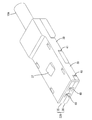
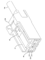
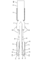
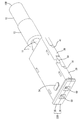
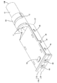
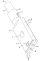
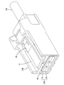
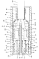
- Example 1 of this invention is a disassembled perspective view of a UTP connector. It is a top view of the UTP connection terminal connected to each electric wire of a UTP cable. It is a perspective view which shows the state in which the UTP connection terminal was accommodated in the accommodating part of a UTP dielectric material. It is a perspective view which shows the state by which the UTP connection terminal was coat
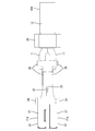
- FIG. 10 is a schematic diagram of the embodiment shown in FIGS.
- FIG. 7 is a view corresponding to FIG. 6 of another embodiment in which the protrusions of the UTP connection terminal are arranged to face each other.
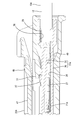
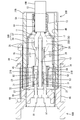
- FIG. 7 is a schematic diagram of another aspect shown in FIG. It is a disassembled perspective view of an STP connector. It is a bottom view of a lower outer conductor. It is a bottom view of an upper outer conductor. It is sectional drawing of the STP connection terminal connected to the STP cable.
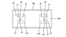
- FIG. 26 is a schematic diagram of the embodiment shown in FIGS.
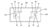
- FIG. 23 is a view corresponding to FIG. 22 in another mode in which the protrusions of the STP connection terminals are arranged to face each other. It is a schematic diagram of another aspect shown in FIG.
- a receiving portion and an elastic contact piece facing the receiving portion are disposed in the box portion, the elastic contact piece protrudes into the box portion with a larger protruding amount than the receiving portion, and the male terminal is the receiving portion.
- the UTP connection terminal is located in the accommodating portion forming the pair of the UTP dielectric, and the receiving portion is located on the inner side in the width direction.
- the elastic contact piece is accommodated so as to be located on the outer side that is separated in the width direction, and the STP electric wire terminal is separated in the accommodating part that forms the pair of the STP dielectric, and the receiving part is separated in the width direction.
- the impedance can be easily adjusted only by reversing the positional relationship between the elastic contact piece and the receiving portion between the UTP cable side and the STP cable side.
- FIGS. 1 and 6 A first embodiment of the present invention will be described with reference to the drawings.
- the connector structure of the first embodiment is used in an in-vehicle communication network system.
- the UTP connector 20A provided at the end of the UTP cable 10A
- FIGS. 3 the STP connector 20B is provided at the end of the STP cable 10B.
- the UTP connector 20A and the STP connector 20B have a structure part that is common or approximate to each other, and it is possible to easily replace the UTP cable 10A and the STP cable 10B while adjusting the impedance. .
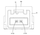
- the UTP connector 20A is fitted to the counterpart UTP connector 90A and includes a UTP connection terminal 21A, a UTP dielectric 22A, and a UTP housing 23A.
- the STP connector 20B is fitted to the mating STP connector 90B and includes an STP connection terminal 21B, an STP dielectric 22B, an outer conductor 24B, and an STP housing 23B.
- the words “UTP” and “STP” in the names of the respective members are simply added for the sake of convenience.
- the UTP cable 10 ⁇ / b> A includes a pair of twisted electric wires 11 and a sheath 12 surrounding each electric wire 11.
- the electric wire 11 includes a conductor portion and a covering portion that surrounds the conductor portion. The end of each electric wire 11 is exposed from the sheath 12 and connected to the UTP connection terminal 21A.
- the UTP connection terminals 21A connected to the electric wires 11 of the UTP cable 10A are configured in the same shape. As shown in FIG. 9, the UTP connection terminal 21A is connected to a male terminal 91 provided on the counterpart UTP connector 90A when the UTP connector 20A and the counterpart UTP connector 90A are fitted. As shown in FIGS. 2 and 6, the UTP connection terminal 21A is integrally formed by bending a conductive metal plate material or the like, and has an elongated shape in the front-rear direction (left-right direction in FIG. 2) as a whole. .
- the UTP connection terminal 21A has a strip-like substrate portion 25 along the front-rear direction. As shown in FIG. 6, when the UTP connection terminal 21A is accommodated in each accommodating portion 26, which will be described later, of the UTP dielectric 22A, the substrate portions 25 of the UTP connection terminals 21A are disposed on the inner side in the width direction.
- a substantially rectangular tube-shaped box portion 27 is provided at the front end portion of the substrate portion 25, and an open barrel-like barrel portion 28 is provided at the rear end portion of the substrate portion 25.
- the barrel portion 28 is electrically and mechanically connected to the conductor portion and the covering portion of the electric wire 11.
- a caulking ring 29 separate from the UTP connection terminal 21A is crimped and connected to the end of the sheath 12 of the UTP cable 10A.
- the caulking ring 29 has a portion that projects in close contact with both sides in the width direction by crimping.
- the receiving portion 31 and the elastic contact piece 32 are arranged in the width direction (in the direction perpendicular to the insertion direction of the male terminal 91 with respect to the box portion 27, as shown in FIG. Project to face each other.
- the receiving part 31 is fixed in a trapezoidal cross section on the substrate part 25 side.
- the elastic contact piece 32 is provided on the top plate portion 33 on the side opposite to the substrate portion 25 so as to protrude forward in a cantilevered manner.
- the amount of protrusion into the box part 27 (vertical direction in FIG. 6) is larger in the elastic contact piece 32 than in the receiving part 31.
- the UTP connection terminal 21 ⁇ / b> A when the UTP connection terminal 21 ⁇ / b> A is connected to the male terminal 91, a tab portion 92 described later of the male terminal 91 is inserted into the box portion 27, and the inserted tab portion 92 is connected to the receiving portion 31.
- the elastic contact piece 32 is elastically sandwiched between the elastic contact pieces 32.
- the box portion 27 has the insertion region 53 of the male terminal 91 between the receiving portion 31 and the elastic contact piece 32.
- the UTP connection terminal 21 ⁇ / b> A has a protrusion 34 that protrudes from one end side of the top plate portion 33 to the outside (in the state accommodated in the accommodation portion 26).
- the UTP dielectric 22A is made of synthetic resin, and includes an upper dielectric 35 and a lower dielectric 36 that can be divided vertically as shown in FIGS.
- the upper dielectric 35 has a substantially rectangular plate shape in plan view, and has a lock projection 37 that can be locked to the UTP housing 23A at the center in the width direction of the upper surface.
- the lower surface of the upper dielectric 35 is provided with a recess 38 (see FIG. 7) for positioning the upper part of each UTP connection terminal 21A in a parallel state and positioning the upper part of the crimping ring 29.
- a pair of front and rear mounting pieces 39 are provided protruding downward.
- the lower dielectric 36 has a plate-like shape that is substantially rectangular in plan view, and has a pair of front and rear mounting receptacles 41 at both ends in the width direction, and mounting projections 42 on the inner surface of the mounting receptacle 41. have.
- a mounting piece 39 is fitted to each mounting receiving portion 41, and the tip portion of the mounting piece 39 hooks and locks the mounting protrusion 42, whereby the lower dielectric 36 and the upper dielectric 35 connect the UTP connection terminal 21A. It is held in a united state by being sandwiched.
- a housing portion 26 that positions and holds the lower portion of each UTP connection terminal 21 ⁇ / b> A in a parallel state is provided at a position facing the recess 38 of the upper dielectric 35.
- the accommodating portion 26 has a cross-sectional shape corresponding to the outer shape of the UTP connection terminal 21A, and is provided in pairs on both sides in the width direction across the thin partition wall 43 so as to correspond to each UTP connection terminal 21A. Yes.
- the substrate portion 25 of each UTP connection terminal 21 ⁇ / b> A is arranged along the wall surface of the partition wall 43.
- a tab insertion hole 69 is formed on the front surface of the UTP dielectric 22A so as to communicate with the accommodating portion 26 and the recess 38 and insert the tab portion 92. Is provided with an opening.
- one of the accommodating portions 26 (upper side in FIG. 6) has an angular concave recess 44 on the side surface on the outer side in the width direction, and the other accommodating portion 26 extends upward from the side edge on the outer side in the width direction. It has a plate-like projecting piece portion 45 that protrudes into the plate.
- the protrusions 34 of the UTP connection terminals 21A housed in one housing part 26 are fitted and inserted into the recesses 44 in a positioning state (see FIG. 6), and the projecting piece part 45 is inserted into the other housing part 26.
- the protrusion 34 of the accommodated UTP connection terminal 21A is placed and supported (see FIG. 3).
- the protrusion 34 of the UTP connection terminal 21A accommodated in one accommodation part 26 is inserted deeply into the recess 44 and arranged on the lower side, and the protrusion 34 of the UTP connection terminal 21A accommodated in the other accommodation part 26 is In addition, it is arranged on the upper side so as to be supported by the projecting piece 45. Further, a concave portion 46 for positioning and holding the lower portion of the caulking ring 29 is provided on the lower surface of the lower dielectric 36 so as to be continuous with the rear of the housing portion 26.
- the UTP housing 23A is made of synthetic resin and has a housing body 47 having a substantially rectangular tube shape.
- a lock arm 48 protrudes from the center of the upper surface of the housing main body 47 in the width direction.
- the lock arm 48 is configured to extend rearward from the front end of the upper surface of the housing main body 47 in a cantilevered manner, elastically locking the lock receiving portion 93 of the counterpart UTP connector 90A, and
- the side UTP connector 90A is held in a fitted state.
- the inside of the housing main body 47 is opened as the insertion portion 49 in the front-rear direction.
- the insertion portion 49 has a cross-sectional shape corresponding to the outer shape of the UTP dielectric 22A, and the UTP dielectric 22A can be fitted therein.
- a lance 51 that projects forward in a cantilevered manner is provided so as to be able to bend and deform.
- the UTP dielectric 22A is inserted into the insertion portion 49 from the rear, and after the lock projection 37 bends and deforms the lance 51, the lance 51 returns and engages the lock projection 37, thereby holding the UTP housing 23A.
- the mating UTP connector 90A has a hood portion 94 made of synthetic resin.
- the hood portion 94 is supported by a circuit board (not shown), and the UTP housing 23A can be fitted therein.
- a lock receiving portion 93 On the inner surface of the upper wall of the hood portion 94, a lock receiving portion 93 that is locked to the lock arm 48 is provided.
- pegs 95 made of a metal plate material are attached to the outer surfaces of both side walls of the hood portion 94. Since the peg 95 is soldered to the surface of the circuit board, the counterpart UTP connector 90A is fixed to the circuit board via the peg 95.
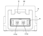
- a pair of male terminals 91 are attached to the hood portion 94 in the width direction.
- Each male terminal 91 has a rectangular shape (square pin shape) as a whole, and has a bent portion in the middle in the length direction.
- Each male terminal 91 has a tab portion 92 protruding into the hood portion 94.
- the tab portion 92 of each male terminal 91 has a flat cross-sectional shape in the width direction (see FIG. 10), and is arranged in parallel with a distance in the width direction corresponding to each UTP connection terminal 21A. .
- the male terminal 91 has a portion protruding to the outside of the hood portion 94, and this portion is mounted on the surface of a circuit board (not shown) and connected by soldering.
- the STP cable 10 ⁇ / b> B includes a pair of twisted electric wires 11, a shield conductor 13 such as a braided wire that surrounds and shields each electric wire 11, and a sheath 12 that surrounds the shield conductor 13.
- the end portions of the electric wires 11 and the end portions of the shield conductors 13 are exposed from the sheath 12, and the end portions of the shield conductors 13 are folded and covered on the outer peripheral side of the sheath 12.
- the end of each electric wire 11 is connected to the STP connection terminal 21B.
- the STP connection terminals 21B connected to the electric wires 11 of the STP cable 10B are configured in the same shape. As shown in FIG. 25, the STP connection terminal 21B is connected to a male terminal 91 provided on the counterpart STP connector 90B when the STP connector 20B and the counterpart STP connector 90B are fitted.
- the STP connection terminal 21B is integrally formed by bending a conductive metal plate material or the like, and has an elongated shape in the front-rear direction as a whole.
- the STP connection terminal 21B has substantially the same configuration as the UTP connection terminal 21A, and includes a substrate part 25, a box part 27, and a barrel part 28.
- the box part 27 and the barrel part 28 of the STP connection terminal 21B have substantially the same shape as the box part 27 and the barrel part 28 of the UTP connection terminal 21A.
- positioning of the receiving part 31 and the elastic contact piece 32 with respect to the box part 27 of STP connection terminal 21B is made into the opposite side to that of UTP connection terminal 21A. That is, as shown in FIG. 16, the receiving portion 31 of the STP connection terminal 21B is provided on the top plate portion 33 side, and the elastic contact piece 32 of the STP connection terminal 21B is provided on the substrate portion 25 side.
- the insertion region 53 of the male terminal 91 in the box portion 27 is eccentric to the substrate portion 25 side in the UTP connection terminal 21A, but is eccentric to the top plate portion 33 side in the STP connection terminal 21B.
- the STP connection terminal 21B has a protrusion 34 protruding outward from one end side of the top plate portion 33, like the UTP connection terminal 21A.
- the STP dielectric 22B is made of synthetic resin, and includes an upper dielectric 35 and a lower dielectric 36 that can be divided vertically as shown in FIGS.
- the upper dielectric 35 has a substantially rectangular plate shape in plan view, and has positioning protrusions 54 for the outer conductor 24B on the upper surface and both side surfaces.
- attachment pieces 39 are provided in the same manner as the upper dielectric 35 of the UTP dielectric 22A.
- the lower dielectric 36 is also provided with an attachment receiving portion 41 and an attachment protrusion 42.
- the STP connector 20B is not provided with the caulking ring 29, and a portion for receiving the caulking ring 29 (a portion corresponding to the recessed portion 46) is required at the rear of each of the upper dielectric 35 and the lower dielectric 36. Therefore, the front-rear dimension of the STP dielectric 22B is shorter than that of the UTP dielectric 22A.
- the lower surface of the upper dielectric 35 is provided with a recess 38 for positioning the upper part of each STP connection terminal 21B in a parallel state
- the upper surface of the lower dielectric 36 is provided with a recess 38 and A housing portion 26 that positions and holds the lower portion of each STP connection terminal 21B in a parallel state is provided at the opposing position.
- the accommodating portion 26 has a cross-sectional shape corresponding to the outer shape of the STP connection terminal 21B, and is provided in pairs on both sides in the width direction across the partition wall 43 so as to correspond to each STP connection terminal 21B.
- each STP connection terminal 21 ⁇ / b> B is arranged in a back-to-back state in the housing portion 26 in which the substrate portion 25 is disposed along the wall surface of the partition wall 43 and is paired in the width direction. This is the same for each UTP connection terminal 21A.
- the thickness (dimension in the width direction) of the partition wall 43 of the STP dielectric 22B is larger than the thickness of the partition wall 43 of the UTP dielectric 22A.
- each housing portion 26 of the STP dielectric 22B is made larger than the separation distance in the width direction of each housing portion 26 of the UTP dielectric 22A.
- a tab portion 92 is formed on the front surface of the STP dielectric 22B so as to communicate with the accommodating portion 26 and the recess 38.
- a tab insertion hole 69 to be inserted is opened.
- one (the upper side in FIG. 22) accommodating portion 26 has a plate-like protruding piece portion 45 protruding upward from the side edge on the outer side in the width direction, and the other accommodating portion 26 is An angular recess 44 is provided on the outer side in the width direction.
- a protrusion 34 of the STP connection terminal 21B accommodated in one accommodation portion 26 is placed and supported on the protrusion 45, and the STP connection terminal 21B accommodated in the other accommodation portion 26 is supported in the recess 44.
- the protrusion 34 is fitted and inserted in the positioning state.
- the STP connection terminal 21 ⁇ / b> B accommodated in one accommodation part 26 is arranged on the upper side so as to be supported by the projecting piece part 45 and accommodated in the other accommodation part 26.
- the STP connection terminal 21B is inserted deeply into the recess 44 and disposed on the lower side.
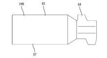
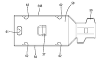
- the outer conductor 24 ⁇ / b> B is made of a conductive metal, and includes an upper outer conductor 56 and a lower outer conductor 57 that can be divided vertically as shown in FIGS. 13 and 20.
- the upper outer conductor 56 has an upper shell portion 58 that is substantially rectangular in plan view, and an open barrel-shaped upper barrel portion 59 that continues to the rear of the upper shell portion 58.
- the upper shell portion 58 is disposed so as to cover the upper dielectric 35 from above.
- the flat plate portion of the upper shell portion 58 has a lock protrusion 37 at the center in the width direction of the upper surface, and has an upper positioning hole 61 in front of the lock protrusion 37.
- the upper shell portion 58 has side plate portions that hang down from both ends in the width direction of the flat plate portion, and has a pair of front and rear holding protrusions 62 on the inner surface of the side plate portion.
- the upper barrel portion 59 has a protruding piece portion that is shifted in the front-rear direction from both side edges in the width direction and protrudes downward.
- the lower outer conductor 57 has a lower shell portion 63 that is substantially rectangular in plan view, and an open barrel-shaped lower barrel portion 64 that continues to the rear of the lower shell portion 63. .
- the lower shell portion 63 is disposed so as to cover the lower dielectric 36 from below.
- the lower shell part 63 has the side-plate part which stands up from the width direction both ends of a flat plate part, and has the holding hole 65 of a pair of front and back in a side-plate part.
- a lower positioning hole 66 is provided at the upper end of the side plate portion of the lower shell portion 63 so as to open at the upper end.
- the lower barrel portion 64 has a protruding piece portion that is displaced in the front-rear direction from the both edges in the width direction and protrudes upward.
- the side plate portion of the upper shell portion 58 covers the side plate portion of the lower shell portion 63 from the outside. As shown, each holding projection 62 is inserted and locked in the holding hole 65. In addition, a pair of front and rear protruding pieces of the upper barrel portion 59 and the lower barrel portion 64 are arranged.
- the STP housing 23B is made of synthetic resin and has a housing body 47 having a substantially rectangular tube shape.
- the STP housing 23B has substantially the same shape as the UTP housing 23A, and includes a lock arm 48, an insertion portion 49, and a lance 51 that have the same form (shape and arrangement) as the UTP housing 23A.
- the locking partner of the lance 51 is not the STP dielectric 22B but the upper outer conductor 56.
- the mating STP connector 90B has a hood portion 94 made of synthetic resin.
- the counterpart STP connector 90B has substantially the same configuration as the counterpart UTP connector 90A, and includes a hood portion 94, a lock receiving portion 93, a peg 95, and a pair of male terminals 91.
- the distance in the width direction of each male terminal 91 of the mating STP connector 90B is greater than the distance in the width direction of the male terminal 91 of the mating UTP connector 90A (see FIGS. 8 and 24).
- each UTP connection terminal 21 ⁇ / b> A is positioned and inserted from above into the accommodating portion 26 of the lower dielectric 36, and the caulking ring 29 fitted to the UTP cable 10 ⁇ / b> A is lowered. It is positioned and inserted into the recessed portion 46 of the side dielectric 36.
- the upper dielectric 35 is placed on the lower dielectric 36 from above.
- each UTP connection terminal 21 ⁇ / b> A is arranged in the UTP dielectric 22 ⁇ / b> A with the mutual substrate portions 25 being close to each other in the width direction via the partition wall 43, and the insertion region of the male terminal 91 in the box portion 27. 53 is also arranged close to the width direction.
- the UTP dielectric 22A is inserted into the insertion portion 49 of the UTP housing 23A from the rear.
- the lance 51 elastically locks the lock protrusion 37 of the UTP dielectric 22A, and the UTP dielectric 22A becomes the UTP housing 23A. Is held in a state of being prevented from coming off.
- Each STP connection terminal 21B is arranged in the STP dielectric 22B in a state where the mutual substrate parts 25 are separated from each other in the width direction through the partition wall 43 as compared with the case of the UTP connector 20A.
- the insertion region 53 of the male terminal 91 is also arranged farther in the width direction than in the case of the UTP connector 20A.
- the STP dielectric 22 ⁇ / b> B is placed on the lower shell portion 63 of the lower outer conductor 57.
- the positioning protrusions 54 provided on both side surfaces of the upper dielectric 35 are fitted into the lower positioning holes 66 of the lower shell 63 so that the lower outer conductor 57 is moved back and forth with respect to the STP dielectric 22B.
- the lower barrel portion 64 is disposed to face the shield conductor 13 exposed on the outer peripheral side of the STP cable 10B from below. In this state, the lower barrel portion 64 is connected to the shield conductor 13 of the STP cable 10B by crimping.
- the upper outer conductor 56 is placed on the lower outer conductor 57 so as to cover the STP dielectric 22B from above.
- the upper outer conductor 56 and the lower outer conductor 57 (outer conductor 24B) are held in the division restricted state by the locking of the holding protrusion 62 and the holding hole 65.
- the positioning protrusion 54 provided on the upper surface of the upper dielectric 35 is fitted into the upper positioning hole 61 of the upper shell 58 so that the upper outer conductor 56 is fitted to the STP dielectric 22B in the front-rear direction.
- the upper barrel part 59 is arrange
- the upper barrel portion 59 is connected to the shield conductor 13 of the STP cable 10B by crimping.
- the shield conductor 13 is connected to the outer conductor 24B, and the periphery of the STP connection terminal 21B is surrounded by the outer conductor 24B via the STP dielectric 22B.
- the outer conductor 24B including the STP connection terminals 21B and the STP dielectric 22B in a combined state is inserted into the insertion portion 49 of the STP housing 23B from the rear.
- the lance 51 elastically locks the lock projection 37 of the outer conductor 24B, and the outer conductor 24B is prevented from coming off from the STP housing 23B. Kept in a state.
- the lock arm 48 elastically locks the lock receiving portion 93, and both the connectors 20B and 90B are held in the disengagement restricted state.
- the tab portion 92 of each male terminal 91 is inserted and connected to the insertion region 53 in the box portion 27 of each STP connection terminal 21B.
- the tab portion 92 of each male terminal 91 is arranged in a state of being separated in the width direction as compared with the case of the UTP connector 20A.
- the outer conductor 24 ⁇ / b> B is connected to the ground plate 68 installed in the hood portion 94.
- the impedance can be reduced by arranging the UTP connection terminals 21A closer to the STP connection terminals 21B in a state where the UTP connection terminals 21A are accommodated in the accommodating portions 26 paired in the width direction. Impedance can also be increased by disposing the connection terminals 21B away from the UTP connection terminals 21A in a state where the connection terminals 21B are accommodated in the accommodating portions 26 that are paired in the width direction.
- the UTP connector 20A and the STP connector 20B have substantially the same configuration except that the STP connector 20B has the outer conductor 24B, and there is no significant structural difference between the configurations. Therefore, when the UTP cable 10A is replaced with the STP cable 10B, or when the STP cable 10B is replaced with the UTP cable 10A, it is not necessary to greatly change the connector structure, and the cost can be reduced.
- the elastic contact piece 32 is located on the outer side in the width direction, and the receiving portion 31 is located on the inner side in the width direction.
- the elastic contact piece 32 is positioned on the inner side in the width direction, and the receiving portion 31 is positioned on the outer side in the width direction. In adjusting the impedance, it is only necessary to reverse the positional relationship between the elastic contact piece 32 and the receiving portion 31 between the UTP connector 20A and the STP connector 20B. Reduction can be achieved.
- the above-described UTP connection terminals 21A shown in FIGS. 1 to 10 are accommodated in the accommodating portions 26 that make a pair in the width direction so that the protrusions 34 are positioned on the outer side in the width direction.
- the accommodating portions 26 that make a pair in the width direction are provided with a concave portion 44 and a protruding piece portion 45 for receiving the protrusions 34 at positions outside the width direction, respectively.
- the above-described STP connection terminals 21B shown in FIGS. 13 to 26 are also accommodated in the accommodating portions 26 that make a pair in the width direction so that the protrusions 34 are located on the outer side in the width direction.
- the housing portion 26 is formed with a concave portion 44 and a projecting piece portion 45 for receiving the projecting portions 34 at positions outside in the width direction.
- the UTP connection terminal 21C is accommodated in the accommodating portion 26 that makes a pair in the width direction so that the protrusions 34 are positioned to face each other in the width direction.
- the accommodating portions 26 forming a pair are provided with a concave portion 44 and a protruding piece portion 45 for receiving the protruding portions 34 at positions on the inner side in the width direction.
- the STP connection terminal 21D of another aspect shown in FIG. 27 is also accommodated in the accommodating portion 26 that is paired in the width direction so that the protrusions 34 are positioned to face each other on the inner side in the width direction.
- the housing portion 26 is formed with a recessed portion 44 and a projecting piece portion 45 for receiving the projecting portion 34 at a position inside the width direction.
- the UTP connection terminal 21C is closer to each other in the width direction than the case where the insertion region 53 of the male terminal 91 in the box portion 27 is accommodated in the accommodating portion 26 that is paired in the width direction, compared to the case of the STP connection terminal 21D.
- the STP connection terminal 21 ⁇ / b> D according to another aspect is arranged in a state where the insertion region 53 of the male terminal 91 in the box portion 27 is accommodated in the accommodating portion 26 that is paired in the width direction, compared to the case where the UTP connection terminal 21 ⁇ / b> C is used.
- both the UTP dielectric and the STP dielectric can be divided vertically, but according to the present invention, at least one of the UTP dielectric and the STP dielectric is integrally formed so as not to be divided. May be.
- the outer conductor of the STP connector can be divided vertically, but according to the present invention, the outer conductor may be integrally formed so as not to be divided.
- each accommodating portion of the STP dielectric is made larger than the widthwise separation distance of each accommodating portion of the UTP dielectric, but according to the present invention, the STP dielectric
- the distance in the width direction of each accommodating portion may be substantially the same as the distance in the width direction of each accommodating portion of the UTP dielectric.
- Two or more protrusions may be provided on the box portion.
Landscapes
- Details Of Connecting Devices For Male And Female Coupling (AREA)
- Coupling Device And Connection With Printed Circuit (AREA)
Abstract
L'invention concerne une structure de connecteur au moyen de laquelle les positions d'un câble STP (10B) et d'un câble UTP (10A) peuvent être commutées sans changement structural majeur. Des bornes de connexion UTP (21A) connectées à chaque fil électrique (11) dans le câble UTP (10A) sont logées dans une section de logement (26) formant une paire de corps diélectriques UTP (22A), ces dernières étant logées dans la même forme les unes par rapport aux autres et de sorte que des zones d'insertion (53) pour des bornes mâles (91) se rapprochent entre elles dans le sens de la largeur. Des bornes de connexion STP (21B) connectées à chaque fil électrique (11) dans le câble STP (10B) sont logées dans une section de logement (26) formant une paire de corps diélectriques STP (22B), ces dernières étant logées dans la même forme les unes par rapport aux autres et de sorte que des zones d'insertion (53) pour des bornes mâles (91) soient davantage espacées entre elles dans le sens de la largeur que pour les bornes de connexion UTP (21A).
Priority Applications (3)
| Application Number | Priority Date | Filing Date | Title |
|---|---|---|---|
| US16/340,419 US10622764B2 (en) | 2016-10-12 | 2017-09-21 | Connector structure |
| DE112017005157.6T DE112017005157B4 (de) | 2016-10-12 | 2017-09-21 | Verbinderstruktur |
| CN201780062423.8A CN109845046B (zh) | 2016-10-12 | 2017-09-21 | 连接器结构 |
Applications Claiming Priority (2)
| Application Number | Priority Date | Filing Date | Title |
|---|---|---|---|
| JP2016200511A JP6729272B2 (ja) | 2016-10-12 | 2016-10-12 | コネクタ構造 |
| JP2016-200511 | 2016-10-12 |
Publications (1)
| Publication Number | Publication Date |
|---|---|
| WO2018070201A1 true WO2018070201A1 (fr) | 2018-04-19 |
Family
ID=61905377
Family Applications (1)
| Application Number | Title | Priority Date | Filing Date |
|---|---|---|---|
| PCT/JP2017/034003 Ceased WO2018070201A1 (fr) | 2016-10-12 | 2017-09-21 | Structure de connecteur |
Country Status (5)
| Country | Link |
|---|---|
| US (1) | US10622764B2 (fr) |
| JP (1) | JP6729272B2 (fr) |
| CN (1) | CN109845046B (fr) |
| DE (1) | DE112017005157B4 (fr) |
| WO (1) | WO2018070201A1 (fr) |
Cited By (1)
| Publication number | Priority date | Publication date | Assignee | Title |
|---|---|---|---|---|
| TWI692155B (zh) * | 2019-04-19 | 2020-04-21 | 宣德科技股份有限公司 | 連接系統 |
Families Citing this family (17)
| Publication number | Priority date | Publication date | Assignee | Title |
|---|---|---|---|---|
| KR101994984B1 (ko) | 2012-07-16 | 2019-07-01 | 콤스코프 인코포레이티드 오브 노스 캐롤라이나 | 균형 잡힌 핀 및 소켓 커넥터들 |
| GB2547958B (en) | 2016-03-04 | 2019-12-18 | Commscope Technologies Llc | Two-wire plug and receptacle |
| JP6769353B2 (ja) * | 2017-03-13 | 2020-10-14 | 株式会社オートネットワーク技術研究所 | 端子ユニット及びコネクタ |
| US11652322B2 (en) | 2017-04-24 | 2023-05-16 | Commscope Technologies Llc | Connectors for a single twisted pair of conductors |
| WO2018227057A1 (fr) | 2017-06-08 | 2018-12-13 | Commscope Technologies Llc | Connecteurs pour une paire torsadée unique de conducteurs |
| WO2019147774A1 (fr) * | 2018-01-26 | 2019-08-01 | Commscope Technologies Llc | Connecteurs pour paire torsadée unique de conducteurs |
| AU2019223204B2 (en) | 2018-02-26 | 2024-06-06 | Commscope Technologies Llc | Connectors and contacts for a single twisted pair of conductors |
| JP6887458B2 (ja) * | 2019-03-12 | 2021-06-16 | 住友電装株式会社 | コネクタ |
| US11894637B2 (en) | 2019-03-15 | 2024-02-06 | Commscope Technologies Llc | Connectors and contacts for a single twisted pair of conductors |
| EP3783751A1 (fr) * | 2019-08-20 | 2021-02-24 | Aptiv Technologies Limited | Connecteur pour applications automobiles |
| WO2021067268A1 (fr) | 2019-09-30 | 2021-04-08 | Commscope Technologies Llc | Panneau de couplage à haute densité |
| US12316055B2 (en) | 2019-09-30 | 2025-05-27 | Commscope Technologies Llc | Couplers for single pair connectors |
| DE102020117772A1 (de) | 2020-07-06 | 2022-01-13 | Harting Electric Gmbh & Co. Kg | Datenübertragungsmodul |
| US20240079814A1 (en) * | 2021-01-21 | 2024-03-07 | Commscope Technologies Llc | Connector for a single twisted pair of conductors |
| US12199372B2 (en) | 2021-02-26 | 2025-01-14 | Commscope Technologies Llc | Couplers for single pair connectors |
| WO2022264799A1 (fr) * | 2021-06-18 | 2022-12-22 | 株式会社オートネットワーク技術研究所 | Connecteur |
| JP7563321B2 (ja) * | 2021-07-27 | 2024-10-08 | 株式会社オートネットワーク技術研究所 | コネクタ |
Citations (6)
| Publication number | Priority date | Publication date | Assignee | Title |
|---|---|---|---|---|
| JP2009135122A (ja) * | 1999-07-16 | 2009-06-18 | Molex Inc | コネクタ |
| JP2015053194A (ja) * | 2013-09-09 | 2015-03-19 | 矢崎総業株式会社 | 多芯ケーブルおよび多芯ケーブルの製造方法 |
| JP2015149189A (ja) * | 2014-02-06 | 2015-08-20 | 第一精工株式会社 | コネクタ端子 |
| JP2016039046A (ja) * | 2014-08-08 | 2016-03-22 | 住友電装株式会社 | コネクタハウジング |
| JP2016115625A (ja) * | 2014-12-17 | 2016-06-23 | 株式会社オートネットワーク技術研究所 | コネクタ及び電線ユニット |
| WO2016132855A1 (fr) * | 2015-02-16 | 2016-08-25 | アルプス電気株式会社 | Borne de connexion et structure de connexion de bornes |
Family Cites Families (32)
| Publication number | Priority date | Publication date | Assignee | Title |
|---|---|---|---|---|
| JPS5333632B1 (fr) | 1968-11-29 | 1978-09-14 | ||
| CH586722A5 (fr) | 1973-12-07 | 1977-04-15 | Lonza Ag | |
| JPS5333632A (en) | 1976-09-10 | 1978-03-29 | Ricoh Co Ltd | Micro-amount application development method and its device for electronic photography |
| US4702538A (en) * | 1985-09-20 | 1987-10-27 | Amphenol Corporation | Shielded modular connector for use with shielded twisted pair cable |
| US4786257A (en) * | 1986-09-30 | 1988-11-22 | Minnesota Mining And Manufacturing Company | Shielded cable termination assembly |
| US5538434A (en) * | 1994-05-18 | 1996-07-23 | The Whitaker Corporation | Electrical connector with integral shorting assembly |
| US6203369B1 (en) | 1999-10-25 | 2001-03-20 | 3M Innovative Properties Company | High frequency cable connector having low self-inductance ground return paths |
| US6962503B2 (en) * | 2000-01-10 | 2005-11-08 | Ortronics, Inc. | Unshielded twisted pair (UTP) wire stabilizer for communication plug |
| US6729901B2 (en) * | 2000-09-29 | 2004-05-04 | Ortronics, Inc. | Wire guide sled hardware for communication plug |
| EP1195854A1 (fr) * | 2000-10-05 | 2002-04-10 | Nexans | Fiche modulaire et procédé pour son couplage avec un câble à paire de fils torsadés |
| US6896557B2 (en) * | 2001-03-28 | 2005-05-24 | Ortronics, Inc. | Dual reactance low noise modular connector insert |
| US6431918B1 (en) * | 2001-04-27 | 2002-08-13 | Hon Hai Precisionind. Co., Ltd. | Modular jack connector meeting 1000base-T specifications |
| FR2826788B1 (fr) * | 2001-06-28 | 2003-09-26 | Arnould App Electr | Prise de courants faibles du type "prise (jack) modulaire" |
| US6439920B1 (en) * | 2001-09-18 | 2002-08-27 | Surtec Industries Inc. | Electronic connector plug for high speed transmission |
| US7150657B2 (en) * | 2003-05-23 | 2006-12-19 | Nordx/Cdt Inc. | Wire lead guide and method for terminating a communications cable |
| US7601024B2 (en) * | 2007-05-07 | 2009-10-13 | Ortronics, Inc. | Shielded connector assembly for preterminated systems |
| US8758047B2 (en) * | 2007-05-07 | 2014-06-24 | Ortronics, Inc. | Port replication assembly with adapter cable and related methods of use |
| JP5087487B2 (ja) | 2008-07-22 | 2012-12-05 | 矢崎総業株式会社 | コネクタ |
| US8308509B2 (en) * | 2009-11-03 | 2012-11-13 | Cisco Technology, Inc. | Multiple-position modular connector employing shielded or filtered signal conductors for reducing electrical noise |
| CN102244324B (zh) * | 2010-05-12 | 2016-01-06 | 富士康(昆山)电脑接插件有限公司 | 线缆连接器 |
| US8715016B2 (en) * | 2010-05-25 | 2014-05-06 | Tyco Electronics Corporation | Electrical connector with signal and power connections |
| JP5066243B2 (ja) * | 2010-06-08 | 2012-11-07 | ヒロセ電機株式会社 | 電気コネクタ、およびツイストペアケーブルと電気コネクタとの接続方法 |
| JP5333632B2 (ja) | 2012-07-19 | 2013-11-06 | 株式会社オートネットワーク技術研究所 | シールドコネクタ |
| CN102751639B (zh) * | 2012-07-27 | 2015-07-22 | 曙光信息产业(北京)有限公司 | PCIe电气信号传输线缆 |
| US8858268B2 (en) * | 2013-03-14 | 2014-10-14 | Commscope, Inc. Of North Carolina | Communications plugs and patch cords with mode conversion control circuitry |
| US9520210B1 (en) * | 2013-06-13 | 2016-12-13 | Superior Essex Communications Lp | Shielded twisted pair communication cables |
| EP2854229B1 (fr) | 2013-09-25 | 2019-01-16 | Yazaki Europe Ltd | Connecteur et procédé de son assemblage |
| JP2015130326A (ja) * | 2013-12-10 | 2015-07-16 | デルファイ・テクノロジーズ・インコーポレーテッド | 遮蔽ケーブルアセンブリ |
| DE102015200058A1 (de) | 2014-01-10 | 2015-07-16 | Dai-Ichi Seiko Co., Ltd. | Verriegelungsarm und elektrischer verbinder, der diesen umfasst |
| US9805844B2 (en) * | 2014-06-24 | 2017-10-31 | Commscope Technologies Llc | Twisted pair cable with shielding arrangement |
| JP6729273B2 (ja) * | 2016-10-12 | 2020-07-22 | 株式会社オートネットワーク技術研究所 | コネクタ構造 |
| JP6495218B2 (ja) * | 2016-10-12 | 2019-04-03 | 株式会社オートネットワーク技術研究所 | コネクタ構造 |
-
2016
- 2016-10-12 JP JP2016200511A patent/JP6729272B2/ja active Active
-
2017
- 2017-09-21 US US16/340,419 patent/US10622764B2/en active Active
- 2017-09-21 CN CN201780062423.8A patent/CN109845046B/zh active Active
- 2017-09-21 WO PCT/JP2017/034003 patent/WO2018070201A1/fr not_active Ceased
- 2017-09-21 DE DE112017005157.6T patent/DE112017005157B4/de active Active
Patent Citations (6)
| Publication number | Priority date | Publication date | Assignee | Title |
|---|---|---|---|---|
| JP2009135122A (ja) * | 1999-07-16 | 2009-06-18 | Molex Inc | コネクタ |
| JP2015053194A (ja) * | 2013-09-09 | 2015-03-19 | 矢崎総業株式会社 | 多芯ケーブルおよび多芯ケーブルの製造方法 |
| JP2015149189A (ja) * | 2014-02-06 | 2015-08-20 | 第一精工株式会社 | コネクタ端子 |
| JP2016039046A (ja) * | 2014-08-08 | 2016-03-22 | 住友電装株式会社 | コネクタハウジング |
| JP2016115625A (ja) * | 2014-12-17 | 2016-06-23 | 株式会社オートネットワーク技術研究所 | コネクタ及び電線ユニット |
| WO2016132855A1 (fr) * | 2015-02-16 | 2016-08-25 | アルプス電気株式会社 | Borne de connexion et structure de connexion de bornes |
Cited By (1)
| Publication number | Priority date | Publication date | Assignee | Title |
|---|---|---|---|---|
| TWI692155B (zh) * | 2019-04-19 | 2020-04-21 | 宣德科技股份有限公司 | 連接系統 |
Also Published As
| Publication number | Publication date |
|---|---|
| CN109845046A (zh) | 2019-06-04 |
| US20190296491A1 (en) | 2019-09-26 |
| JP6729272B2 (ja) | 2020-07-22 |
| DE112017005157T5 (de) | 2019-06-27 |
| DE112017005157B4 (de) | 2022-11-10 |
| CN109845046B (zh) | 2020-05-19 |
| US10622764B2 (en) | 2020-04-14 |
| JP2018063793A (ja) | 2018-04-19 |
Similar Documents
| Publication | Publication Date | Title |
|---|---|---|
| WO2018070201A1 (fr) | Structure de connecteur | |
| US10763600B2 (en) | Connector structure | |
| WO2018070202A1 (fr) | Structure de connecteur | |
| WO2018070203A1 (fr) | Structure de connecteur | |
| US10819071B2 (en) | Connector structure that is reconfigurable to accommodate either an STP cable or a UTP cable | |
| JP6429078B2 (ja) | シールドコネクタ | |
| CN102891388B (zh) | 屏蔽连接器 | |
| JP5756700B2 (ja) | シールドコネクタ及びシールドコネクタの組立方法 | |
| US20220360033A1 (en) | Couplers for single pair connectors | |
| JP6792537B2 (ja) | シールドコネクタおよびシールドコネクタシステム | |
| JP6847016B2 (ja) | 同軸ケーブル用コネクタ | |
| US20220278476A1 (en) | Couplers for single pair connectors | |
| WO2020137886A1 (fr) | Module de borne et connecteur | |
| JP6711936B2 (ja) | コネクタ構造 | |
| JP6735381B2 (ja) | コネクタ構造 | |
| JP6958589B2 (ja) | 電気コネクタ | |
| JP2026030720A (ja) | L字型通信コネクタ |
Legal Events
| Date | Code | Title | Description |
|---|---|---|---|
| 121 | Ep: the epo has been informed by wipo that ep was designated in this application |
Ref document number: 17861151 Country of ref document: EP Kind code of ref document: A1 |
|
| 122 | Ep: pct application non-entry in european phase |
Ref document number: 17861151 Country of ref document: EP Kind code of ref document: A1 |