WO2018079636A1 - 液晶表示装置及び故障検査方法 - Google Patents
液晶表示装置及び故障検査方法 Download PDFInfo
- Publication number
- WO2018079636A1 WO2018079636A1 PCT/JP2017/038616 JP2017038616W WO2018079636A1 WO 2018079636 A1 WO2018079636 A1 WO 2018079636A1 JP 2017038616 W JP2017038616 W JP 2017038616W WO 2018079636 A1 WO2018079636 A1 WO 2018079636A1
- Authority
- WO
- WIPO (PCT)
- Prior art keywords
- line
- output signal
- circuit
- monitor
- gate
- Prior art date
- Legal status (The legal status is an assumption and is not a legal conclusion. Google has not performed a legal analysis and makes no representation as to the accuracy of the status listed.)
- Ceased
Links
Images







Classifications
-
- G—PHYSICS
- G09—EDUCATION; CRYPTOGRAPHY; DISPLAY; ADVERTISING; SEALS
- G09G—ARRANGEMENTS OR CIRCUITS FOR CONTROL OF INDICATING DEVICES USING STATIC MEANS TO PRESENT VARIABLE INFORMATION
- G09G3/00—Control arrangements or circuits, of interest only in connection with visual indicators other than cathode-ray tubes
- G09G3/20—Control arrangements or circuits, of interest only in connection with visual indicators other than cathode-ray tubes for presentation of an assembly of a number of characters, e.g. a page, by composing the assembly by combination of individual elements arranged in a matrix no fixed position being assigned to or needed to be assigned to the individual characters or partial characters
- G09G3/34—Control arrangements or circuits, of interest only in connection with visual indicators other than cathode-ray tubes for presentation of an assembly of a number of characters, e.g. a page, by composing the assembly by combination of individual elements arranged in a matrix no fixed position being assigned to or needed to be assigned to the individual characters or partial characters by control of light from an independent source
- G09G3/36—Control arrangements or circuits, of interest only in connection with visual indicators other than cathode-ray tubes for presentation of an assembly of a number of characters, e.g. a page, by composing the assembly by combination of individual elements arranged in a matrix no fixed position being assigned to or needed to be assigned to the individual characters or partial characters by control of light from an independent source using liquid crystals
- G09G3/3611—Control of matrices with row and column drivers
- G09G3/3648—Control of matrices with row and column drivers using an active matrix
-
- G—PHYSICS
- G02—OPTICS
- G02F—OPTICAL DEVICES OR ARRANGEMENTS FOR THE CONTROL OF LIGHT BY MODIFICATION OF THE OPTICAL PROPERTIES OF THE MEDIA OF THE ELEMENTS INVOLVED THEREIN; NON-LINEAR OPTICS; FREQUENCY-CHANGING OF LIGHT; OPTICAL LOGIC ELEMENTS; OPTICAL ANALOGUE/DIGITAL CONVERTERS
- G02F1/00—Devices or arrangements for the control of the intensity, colour, phase, polarisation or direction of light arriving from an independent light source, e.g. switching, gating or modulating; Non-linear optics
- G02F1/01—Devices or arrangements for the control of the intensity, colour, phase, polarisation or direction of light arriving from an independent light source, e.g. switching, gating or modulating; Non-linear optics for the control of the intensity, phase, polarisation or colour
- G02F1/13—Devices or arrangements for the control of the intensity, colour, phase, polarisation or direction of light arriving from an independent light source, e.g. switching, gating or modulating; Non-linear optics for the control of the intensity, phase, polarisation or colour based on liquid crystals, e.g. single liquid crystal display cells
- G02F1/1306—Details
- G02F1/1309—Repairing; Testing
-
- G—PHYSICS
- G02—OPTICS
- G02F—OPTICAL DEVICES OR ARRANGEMENTS FOR THE CONTROL OF LIGHT BY MODIFICATION OF THE OPTICAL PROPERTIES OF THE MEDIA OF THE ELEMENTS INVOLVED THEREIN; NON-LINEAR OPTICS; FREQUENCY-CHANGING OF LIGHT; OPTICAL LOGIC ELEMENTS; OPTICAL ANALOGUE/DIGITAL CONVERTERS
- G02F1/00—Devices or arrangements for the control of the intensity, colour, phase, polarisation or direction of light arriving from an independent light source, e.g. switching, gating or modulating; Non-linear optics
- G02F1/01—Devices or arrangements for the control of the intensity, colour, phase, polarisation or direction of light arriving from an independent light source, e.g. switching, gating or modulating; Non-linear optics for the control of the intensity, phase, polarisation or colour
- G02F1/13—Devices or arrangements for the control of the intensity, colour, phase, polarisation or direction of light arriving from an independent light source, e.g. switching, gating or modulating; Non-linear optics for the control of the intensity, phase, polarisation or colour based on liquid crystals, e.g. single liquid crystal display cells
- G02F1/133—Constructional arrangements; Operation of liquid crystal cells; Circuit arrangements
- G02F1/13306—Circuit arrangements or driving methods for the control of single liquid crystal cells
-
- G—PHYSICS
- G02—OPTICS
- G02F—OPTICAL DEVICES OR ARRANGEMENTS FOR THE CONTROL OF LIGHT BY MODIFICATION OF THE OPTICAL PROPERTIES OF THE MEDIA OF THE ELEMENTS INVOLVED THEREIN; NON-LINEAR OPTICS; FREQUENCY-CHANGING OF LIGHT; OPTICAL LOGIC ELEMENTS; OPTICAL ANALOGUE/DIGITAL CONVERTERS
- G02F1/00—Devices or arrangements for the control of the intensity, colour, phase, polarisation or direction of light arriving from an independent light source, e.g. switching, gating or modulating; Non-linear optics
- G02F1/01—Devices or arrangements for the control of the intensity, colour, phase, polarisation or direction of light arriving from an independent light source, e.g. switching, gating or modulating; Non-linear optics for the control of the intensity, phase, polarisation or colour
- G02F1/13—Devices or arrangements for the control of the intensity, colour, phase, polarisation or direction of light arriving from an independent light source, e.g. switching, gating or modulating; Non-linear optics for the control of the intensity, phase, polarisation or colour based on liquid crystals, e.g. single liquid crystal display cells
- G02F1/133—Constructional arrangements; Operation of liquid crystal cells; Circuit arrangements
- G02F1/136—Liquid crystal cells structurally associated with a semi-conducting layer or substrate, e.g. cells forming part of an integrated circuit
- G02F1/1362—Active matrix addressed cells
- G02F1/136286—Wiring, e.g. gate line, drain line
-
- G—PHYSICS
- G09—EDUCATION; CRYPTOGRAPHY; DISPLAY; ADVERTISING; SEALS
- G09G—ARRANGEMENTS OR CIRCUITS FOR CONTROL OF INDICATING DEVICES USING STATIC MEANS TO PRESENT VARIABLE INFORMATION
- G09G3/00—Control arrangements or circuits, of interest only in connection with visual indicators other than cathode-ray tubes
- G09G3/006—Electronic inspection or testing of displays and display drivers, e.g. of LED or LCD displays
-
- G—PHYSICS
- G09—EDUCATION; CRYPTOGRAPHY; DISPLAY; ADVERTISING; SEALS
- G09G—ARRANGEMENTS OR CIRCUITS FOR CONTROL OF INDICATING DEVICES USING STATIC MEANS TO PRESENT VARIABLE INFORMATION
- G09G3/00—Control arrangements or circuits, of interest only in connection with visual indicators other than cathode-ray tubes
- G09G3/20—Control arrangements or circuits, of interest only in connection with visual indicators other than cathode-ray tubes for presentation of an assembly of a number of characters, e.g. a page, by composing the assembly by combination of individual elements arranged in a matrix no fixed position being assigned to or needed to be assigned to the individual characters or partial characters
-
- G—PHYSICS
- G02—OPTICS
- G02F—OPTICAL DEVICES OR ARRANGEMENTS FOR THE CONTROL OF LIGHT BY MODIFICATION OF THE OPTICAL PROPERTIES OF THE MEDIA OF THE ELEMENTS INVOLVED THEREIN; NON-LINEAR OPTICS; FREQUENCY-CHANGING OF LIGHT; OPTICAL LOGIC ELEMENTS; OPTICAL ANALOGUE/DIGITAL CONVERTERS
- G02F1/00—Devices or arrangements for the control of the intensity, colour, phase, polarisation or direction of light arriving from an independent light source, e.g. switching, gating or modulating; Non-linear optics
- G02F1/01—Devices or arrangements for the control of the intensity, colour, phase, polarisation or direction of light arriving from an independent light source, e.g. switching, gating or modulating; Non-linear optics for the control of the intensity, phase, polarisation or colour
- G02F1/13—Devices or arrangements for the control of the intensity, colour, phase, polarisation or direction of light arriving from an independent light source, e.g. switching, gating or modulating; Non-linear optics for the control of the intensity, phase, polarisation or colour based on liquid crystals, e.g. single liquid crystal display cells
- G02F1/133—Constructional arrangements; Operation of liquid crystal cells; Circuit arrangements
- G02F1/136—Liquid crystal cells structurally associated with a semi-conducting layer or substrate, e.g. cells forming part of an integrated circuit
- G02F1/1362—Active matrix addressed cells
- G02F1/136254—Checking; Testing
-
- G—PHYSICS
- G09—EDUCATION; CRYPTOGRAPHY; DISPLAY; ADVERTISING; SEALS
- G09G—ARRANGEMENTS OR CIRCUITS FOR CONTROL OF INDICATING DEVICES USING STATIC MEANS TO PRESENT VARIABLE INFORMATION
- G09G2310/00—Command of the display device
- G09G2310/02—Addressing, scanning or driving the display screen or processing steps related thereto
- G09G2310/0264—Details of driving circuits
- G09G2310/0297—Special arrangements with multiplexing or demultiplexing of display data in the drivers for data electrodes, in a pre-processing circuitry delivering display data to said drivers or in the matrix panel, e.g. multiplexing plural data signals to one D/A converter or demultiplexing the D/A converter output to multiple columns
-
- G—PHYSICS
- G09—EDUCATION; CRYPTOGRAPHY; DISPLAY; ADVERTISING; SEALS
- G09G—ARRANGEMENTS OR CIRCUITS FOR CONTROL OF INDICATING DEVICES USING STATIC MEANS TO PRESENT VARIABLE INFORMATION
- G09G2330/00—Aspects of power supply; Aspects of display protection and defect management
- G09G2330/12—Test circuits or failure detection circuits included in a display system, as permanent part thereof
-
- G—PHYSICS
- G09—EDUCATION; CRYPTOGRAPHY; DISPLAY; ADVERTISING; SEALS
- G09G—ARRANGEMENTS OR CIRCUITS FOR CONTROL OF INDICATING DEVICES USING STATIC MEANS TO PRESENT VARIABLE INFORMATION
- G09G2380/00—Specific applications
- G09G2380/10—Automotive applications
Definitions
- the present invention relates to a liquid crystal display device having an active matrix liquid crystal panel and a failure inspection method thereof.
- in-vehicle liquid crystal display devices are used not only for car navigation but also for instrument panels in which instruments such as speedometers, tachometers, and water thermometers are incorporated.
- instruments such as speedometers, tachometers, and water thermometers
- a warning icon for example.
- a speedometer SM, a tachometer TM, a warning icon WI, and the like are displayed.
- a warning light WL similar to the conventional one is usually arranged adjacent to the display screen D1.
- an abnormality of the in-vehicle device is notified by the warning lamp WL, so that the safety of the passenger is ensured. (Fail safe).
- the present invention provides a liquid crystal display device and a failure inspection method capable of self-diagnosis of a liquid crystal panel failure (source line / gate line open abnormality and short circuit abnormality) with a simple circuit configuration.
- a liquid crystal display device is sealed between a first substrate, a second substrate disposed opposite to the first substrate, and the first substrate and the second substrate.
- the liquid crystal display device includes a source line and a gate line, a pixel electrode, a switching element, a source driver, a gate driver, and a failure inspection circuit.
- the source line and the gate line are arranged in a lattice pattern.
- the pixel electrode is disposed in a pixel region defined by the source line and the gate line.
- the switching element is disposed corresponding to the pixel electrode.
- the source driver drives the source line.
- the gate driver drives the gate line.
- the failure inspection circuit is connected to the source line or the gate line and inspects the source line or the gate line.
- the fault inspection circuit includes a monitor input signal line, a monitor output signal line, a determination circuit that detects the voltage level of the output signal from the monitor output signal line, and an expected value comparison that compares the output from the determination circuit with the expected value.
- a circuit is connected to the source line or the gate line and inspects the source line or the gate line.
- the fault inspection circuit includes a monitor input signal line, a monitor output signal line, a determination circuit that detects the voltage level of the output signal from the monitor output signal line, and an expected value comparison that compares the output from the determination circuit with the expected value.
- a failure inspection method is the failure inspection method for a liquid crystal display device described above, based on an output signal when a gate signal from a gate driver is applied during an image display period. In addition, the gate line is inspected for failure.
- a failure inspection method is the above-described failure inspection method for a liquid crystal display device, and performs a source line failure inspection during a blanking period between a plurality of video display periods.
- FIG. 1 is a diagram illustrating an example of an instrument panel to which a liquid crystal display device is applied.
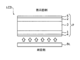
- FIG. 2 is a diagram showing an example of a liquid crystal display device according to an embodiment of the present invention.
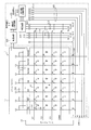
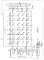
- FIG. 3 is a diagram illustrating an example of a circuit configuration of the active matrix substrate according to the first embodiment.
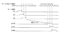
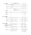
- FIG. 4 is a timing chart showing an example of the driving operation of the gate driver.
- FIG. 5 is a timing chart showing an example of the driving operation of the source driver.
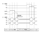
- FIG. 6 is a timing chart showing an example of the relationship between the driving operation of the gate driver and the source driver and video display.
- FIG. 7 is a diagram illustrating an example of a circuit configuration for inspecting the gate line open abnormality and short circuit abnormality.
- FIG. 1 is a diagram illustrating an example of an instrument panel to which a liquid crystal display device is applied.
- FIG. 2 is a diagram showing an example of a liquid crystal display device according to an embodiment of the present invention.
- FIG. 3 is
- FIG. 8 is a timing chart showing an example of a gate line failure inspection result.
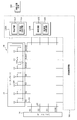
- FIG. 9 is a diagram illustrating an example of a circuit configuration for inspecting an open abnormality and a short abnormality of a source line.
- FIG. 10 is a diagram illustrating an example of an operation when detecting a short-circuit abnormality of a source line.
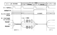
- FIG. 11 is a timing chart showing an example of a failure inspection result (short abnormality) of the source line.
- FIG. 12 is a diagram illustrating an example of an operation when detecting an open abnormality of a source line.
- FIG. 13 is a timing chart showing an example of a failure inspection result (open abnormality) of the source line.
- FIG. 14 is a diagram illustrating an example of a circuit configuration of the active matrix substrate according to the second embodiment.
- FIG. 15 is a diagram illustrating an example of an operation when detecting a short-circuit abnormality of a gate line.
- FIG. 16 is a diagram illustrating an example of an operation when detecting an open abnormality of a gate line.
- FIG. 17 is a diagram illustrating an example of a circuit configuration of an active matrix substrate according to the third embodiment.
- FIG. 18 is a diagram illustrating an example of a circuit configuration of the auxiliary inspection circuit.
- an active matrix type liquid crystal panel before mounting a driver IC (integrated circuit) (source driver and gate driver), a lighting inspection is performed for each pixel in order to check whether the liquid crystal panel operates normally.
- a failure inspection circuit to be performed (hereinafter referred to as “initial failure inspection circuit”) is provided around the display area (for example, Patent Document 1).
- this initial failure inspection circuit is used only for failure inspection at the manufacturing stage, and cannot be used during video display, for example, in a liquid crystal display device after the driver IC is mounted.
- FIG. 2 is a diagram illustrating an example of a liquid crystal display LCD according to an embodiment of the present invention.
- the liquid crystal display device LCD is applied to, for example, an instrument panel of a vehicle, and displays an abnormality warning for instruments and in-vehicle devices.
- the liquid crystal display device LCD has a liquid crystal panel P and a backlight BL disposed on the back side of the liquid crystal panel P.
- the liquid crystal panel P includes an active matrix substrate 1 (first substrate), a counter substrate 2 (second substrate) disposed to face the active matrix substrate 1, and a space between the active matrix substrate 1 and the counter substrate 2.
- the liquid crystal layer 3 is sealed.
- the active matrix substrate 1 and the counter substrate 2 are substrates made of glass, for example.
- a polarizing plate 4 is disposed on the back side of the active matrix substrate 1, and a polarizing plate 5 is disposed on the surface side of the counter substrate 2.
- the counter substrate 2 includes a counter electrode (common electrode), a color filter, and the like (all not shown). A detailed configuration of the active matrix substrate 1 will be described later.
- FIG. 3 is a diagram illustrating an example of a circuit configuration of the active matrix substrate 1 according to the first embodiment.
- the active matrix substrate 1 includes a source line 11 (data line) and a gate line 12 (scanning line) arranged in a lattice pattern, and a pixel region defined by the source line 11 and the gate line 12.
- the active matrix substrate 1 in this embodiment is a substrate for a VGA (Video Graphics Array) panel (640 ⁇ 480 pixels), and includes 1920 source lines 11 and 480 gate lines 12.
- the pixel area defined by the source line 11 and the gate line 12 is a sub-pixel area for each of RGB (red, green, and blue), and one pixel is formed by three sub-pixel areas adjacent in the horizontal direction (gate line direction). An area is configured.
- the switching element 14 is a thin film transistor (TFT: Thin Film Transistor) having a gate electrode, a source electrode, and a drain electrode.
- TFT Thin Film Transistor
- the switching element 14 has a gate electrode connected to the gate line 12, a source electrode connected to the source line 11, and a drain electrode connected to one end of the pixel electrode 13.
- the other end of the pixel electrode 13 is connected to the counter electrode (not shown) via the liquid crystal layer 3.
- the source driver 15 and the gate driver 16 are arranged around the pixel area.
- the gate driver 16 sequentially applies pulsed voltages to the gate lines 12 in order to turn on the switching elements 14 in order.
- the gate driver 16 operates while shifting by one clock with a width of two clocks.
- the source driver 15 supplies a voltage to be applied to the liquid crystal layer 3 through the switching element 14 in the on state (see FIG. 5). Thereby, the pixel corresponding to the switching element 14 in the ON state is turned on.
- the source driver 15 converts the video signal (digital color data) received from the LCD controller (not shown) into an analog voltage and outputs it through the source line 11 at the rising timing of the load signal LD. .
- This voltage is applied to the pixel electrode 13 via the switching element 14.
- the voltage applied to the pixel electrode 13 is determined at the falling edge of the gate signal (see FIG. 6). This voltage is held until the next writing due to the capacitance of the liquid crystal layer 3 itself. With this voltage, the light transmittance in the liquid crystal layer 3 is changed, and a color corresponding to the transmittance is displayed.
- a failure inspection of the source line 11 is performed using this blanking period.
- the failure inspection of the gate line 12 can be performed during video display.
- the failure inspection circuit 100 includes predetermined wiring patterns L1 and L2 (see FIGS. 7 and 9), determination circuits 114 and 105 that detect voltage levels of output signals from the wiring patterns L1 and L2, and determination circuits 114 and 105.
- Expected value comparison circuits 115 and 106 for comparing the output of the output and the expected value.
- the failure inspection circuit 100 uses the source driver 15 or the gate driver 16 to inspect the source line 11 or the gate line 12.
- the comparison results of the expected value comparison circuits 115 and 106 are output to an LCD controller (not shown) or a computer. The LCD controller and the computer execute predetermined processing based on the comparison result.
- the failure inspection circuit 100 includes a first failure inspection circuit 100A (see FIG. 7) for inspecting the gate line 12 and a second failure inspection circuit 100B (see FIG. 9) for inspecting the source line 11. )including.
- FIG. 7 is a diagram illustrating an example of a circuit configuration for inspecting an open abnormality (disconnection) and a short abnormality (short circuit) of the gate line 12.
- the first failure inspection circuit 100A includes a first wiring pattern L1, a first determination circuit 114, and a first expected value comparison circuit 115. At least one of the first determination circuit 114 and the first expected value comparison circuit 115 may be incorporated in the gate driver 16.
- the first wiring pattern L1 includes a first monitor input signal line 111, a first monitor output signal line 112, and a first switching element 113.
- the first monitor input signal line 111 receives the first monitor input signal Gin (Gin1 to Gin3) for inspection of the gate line 12.
- the first monitor output signal line 112 outputs a first monitor output signal Gout (Gout1 to Gout3) based on the first monitor input signal Gin to the first determination circuit 114.
- the first switching element 113 is a transistor having a gate electrode, a source electrode, and a drain electrode. The gate electrode of the first switching element 113 is connected to the opposite side of the gate driver 16 in the gate line 12, the drain electrode is connected to the first monitor input signal line 111, and the source electrode is connected to the monitor output signal line 112.
- FIG. 8 is a timing chart showing an example of a gate line failure inspection result.
- the first monitor output signal Gout shown in FIG. 8 is a voltage level input to the first determination circuit 114.
- the first expected value comparison circuit 115 sets the voltage level to be obtained when the gate line 12 is normal as the first expected value E1, and the voltage level detected by the first determination circuit 114 and the first expected value. By comparing the value E1, an open abnormality and a short abnormality of the gate line 12 are determined.
- the failure inspection of the gate line 12 is performed using, for example, a driving operation of the gate line 12 during video display.
- the gate signals G1 to G480 operate while shifting every clock with a width of 2 clocks.
- the gate line 12 to which the gate signal G is input is an inspection target. That is, the first switching element 113 in which the gate line 12 is connected to the gate electrode is turned on, and the first monitor input signal lines 111 to 1 connected to the first switching element 113 in the on state are turned on.
- the first monitor input signal Gin is input with a clock width.
- a first monitor output signal Gout corresponding to the first monitor input signal Gin from the first monitor input signal line 111 is output to the first determination circuit 114 via the first monitor output signal line 112. .
- the first monitor input signal Gin is input, and the voltage level of the first monitor input signal Gin is “high” (“ Accordingly, the voltage level of the corresponding first monitor output signal Gout also becomes “HIGH”.
- the voltage level of the first monitor output signal Gout is maintained until the next gate signal G is input. For example, when the first monitor input signal Gin1 is input to the first monitor input signal line 111 when the gate signal G1 is input, the voltage level of the first monitor output signal Gout1 becomes “HIGH”. .
- the next gate signal G4 is input, the voltage level of the first monitor output signal Gout1 is “LOW” because the voltage level of the first monitor input signal Gin1 is “LOW” and “LOW” at this time. Become.
- the first switching element 113 is not turned on. Therefore, even when the first monitor input signal Gin is input, the voltage level of the first monitor output signal Gout remains “LOW”. Thereby, the first expected value comparison circuit 115 can detect the open abnormality of the gate line 12.
- the voltage level is lowered during a period in which the voltage level of the first monitor output signal Gout is to be held at “HIGH”. For example, as shown in FIG. 8, when the voltage level of the gate signal G1 becomes “LOW”, the first switching element 113 is turned off, and the voltage level of the first monitor output signal Gout1 is held at “HIGH”. Should be. However, when the gate line 12 to which the gate signal G1 is input and the gate line 12 to which the adjacent gate signal G2 is input are short-circuited, the voltage levels of the two gate lines 12 are input to each gate line 12. The value between the two voltage levels.
- the first switching element 113 that outputs the first monitor output signal Gout1 also becomes a voltage level between “HIGH” and “LOW” by the input of the gate signal G2, and as a result, the first switching element 113 It is not an off state but an indefinite state. At this time, since the first monitor input signal Gin1 is not input, the voltage level of the first monitor output signal Gout1 decreases. Thereby, the first expected value comparison circuit 115 can detect a short circuit abnormality of the gate line 12.
- FIG. 9 is a diagram illustrating an example of a circuit configuration for inspecting an open abnormality (disconnection) and a short abnormality (short circuit) of the source line 11.
- the second failure inspection circuit 100B includes a second wiring pattern L2, a second determination circuit 105, and a second expected value comparison circuit 106. At least one of the second determination circuit 105 and the second expected value comparison circuit 106 may be incorporated in the source driver 15.
- the second wiring pattern L2 includes a second monitor input signal line 103, a second monitor output signal line 104, a second switching element 102, and a control signal line 101.
- the second monitor input signal line 103 receives the second monitor input signal DRGB (DR1, DR2, DG1, DG2, DB1, DB2) for inspection of the source line 11.
- the second monitor output signal line 104 receives the second monitor output signal Sout (Sout1, Sout2) based on the second monitor input signal DRGB or the second monitor output signal Sout based on the input signal from the source driver 15, Output to the second determination circuit 105.
- the second switching element 102 is a transistor having a gate electrode, a source electrode, and a drain electrode.
- the gate electrode of the second switching element 102 is connected to the control signal line 101, the drain electrode is connected to the second monitor input signal line 103, and the source electrode is connected to the opposite side of the source driver 15 in the source line 11. .
- the switch SW provided in the source driver 15 determines whether the second monitor output signal Sout based on the second monitor input signal DRGB or the second monitor output signal Sout based on the input signal from the source driver 15 is the second determination. It is selectively output to the circuit 105.
- FIG. 10 is a diagram illustrating an example of an operation when a short circuit abnormality of the source line 11 is detected.
- FIG. 11 is a timing chart showing an example of a failure inspection result (short abnormality) of the source line 11.
- a monitor output signal shown in FIG. 11 is a voltage level input to the second determination circuit 105.
- the second expected value comparison circuit 106 sets the voltage level to be obtained when the source line 11 is normal as the second expected value E21 and the voltage level detected by the second determination circuit 105 and the second expected value. By comparing the value E21, a short circuit abnormality of the source line 11 is determined.
- the inspection of the short abnormality of the source line 11 is performed, for example, in the first half of the blanking period during video display.
- the voltage level of the control signal TR from the control signal line 101 is set to “LOW”. Accordingly, the second switching element 102 is turned off. In this state, an input signal is input from the source driver 15 corresponding to the source line 11 to be inspected toward the second monitor output signal line 104. A second monitor output signal Sout corresponding to the input signal from the source driver 15 is output to the second determination circuit 105 via the second monitor output signal line 104.
- the voltage level of the second monitor output signal Sout is also from the source driver 15. It becomes a value according to the input signal.
- the voltage level of the second monitor output signal Sout corresponding to the odd-numbered source electrode is “HIGH”.
- the second expected value comparison circuit 106 can detect a short circuit abnormality of the source line 11.
- FIG. 12 is a diagram illustrating an example of an operation when detecting an open abnormality of the source line 11.
- FIG. 13 is a timing chart showing an example of a failure inspection result (open abnormality) of the source line 11.
- the monitor output signal shown in FIG. 13 is a voltage level detected by the second determination circuit 105.
- the second expected value comparison circuit 106 sets the voltage level to be obtained when the source line 11 is normal as the second expected value E22 and the voltage level detected by the second determination circuit 105 and the second expected value.
- the open abnormality of the source line 11 is determined by comparing the value E22.
- the inspection of the open abnormality of the source line 11 is performed, for example, in the second half of the blanking period during video display.
- the voltage level of the control signal TR from the control signal line 101 is set to “HIGH”. Accordingly, the second switching element 102 is turned on. Further, the source line 11 to be inspected is connected to the second monitor output signal line 104 by the switch SW of the source driver 15. In this state, the second monitor input signal DRGB is input from the second monitor input signal line 103 connected to the source line 11 to be inspected. The voltage level of the second monitor input signal DRGB is fixed to the voltage level AVSS of the analog ground terminal. A second monitor output signal Sout based on the second monitor input signal DRGB is output to the second determination circuit 105 via the second monitor output signal line 104.
- the voltage level of the second monitor output signal Sout becomes the level of the monitor input signal DRGB. It becomes equivalent to the voltage level AVSS.
- the second expected value comparison circuit 106 can detect an open abnormality of the source line 11.
- the switches SW connected to S1 and S2 of the source lines 11 are turned on at a time, and two source lines 11 are inspected at a time. Thereafter, all the source lines 11 are inspected by sequentially switching the switches SW to be turned on. When the inspection of all the source lines 11 is not completed in one blanking period, the remaining source lines 11 are inspected in the next blanking period. Note that the number of source lines to be inspected at a time varies depending on the number of wirings.
- the liquid crystal display device LCD includes an active matrix substrate 1 (first substrate), a counter substrate 2 (second substrate) disposed to face the active matrix substrate 1, And an active matrix liquid crystal panel P having a liquid crystal layer 3 sealed between the active matrix substrate 1 and the counter substrate 2.
- the liquid crystal display device LCD includes a source line 11 and a gate line 12, a pixel electrode 13, a switching element 14, a source driver 15, a gate driver 16, and a failure inspection circuit 100.
- the source lines 11 and the gate lines 12 are arranged in a lattice pattern.
- the pixel electrode 13 is disposed in a pixel region defined by the source line 11 and the gate line 12.
- the switching element 14 is disposed corresponding to the pixel electrode 13.
- the source driver 15 drives the source line 11.
- the gate driver 16 drives the gate line 12.
- the failure inspection circuit 100 is connected to the source line 11 or the gate line 12 and inspects the source line 11 or the gate line 12.
- the failure inspection circuit 100 includes monitor input signal lines 111 and 103, monitor output signal lines 112 and 104, determination circuits 114 and 105 that detect voltage levels of output signals from the monitor output signal lines 112 and 104, and a determination circuit. And expected value comparison circuits 115 and 106 for comparing the outputs from 114 and 105 with the expected values E1 and E2.
- the liquid crystal display device LCD According to the liquid crystal display device LCD, a failure of the liquid crystal panel P can be self-diagnosed with a simple circuit configuration.
- the liquid crystal display device LCD displays a warning in the normal display area when the warning display area cannot be displayed due to an abnormality in the source line 11 or the gate line 12.
- the fail-safe function is realized by operating so that failure can be avoided based on self-diagnosis. Therefore, it is not necessary to arrange a warning light, and the device cost can be reduced.
- an active matrix substrate 1A having a different configuration of the failure inspection circuit is applied as the active matrix substrate of the liquid crystal display device LCD instead of the active matrix substrate 1 according to the first embodiment.
- FIG. 14 is a diagram illustrating an example of a circuit configuration of the active matrix substrate 1A according to the second embodiment.
- the active matrix substrate 1A has a source line 11 (data line), a gate line 12 (scanning line), and a pixel electrode 13 (scanning line), like the active matrix substrate 1 according to the first embodiment.
- the source line 11 (data line) and the gate line 12 (scanning line) are arranged in a grid pattern.
- the pixel electrode 13 (sub-pixel electrode) is disposed in a pixel region defined by the source line 11 and the gate line 12.
- the switching element 14 is disposed corresponding to the pixel electrode 13.
- the source driver 15 drives the source line 11.
- the gate driver 16 drives the gate line 12. Since the configuration other than the failure inspection circuit 200 is the same as the configuration of the active matrix substrate 1 according to the first embodiment, the description thereof is omitted.
- the failure inspection circuit 200 compares the output from the determination circuits 105 and 205 for detecting the voltage levels of the output signals from the predetermined wiring patterns L2 and L3, the wiring patterns L2 and L3, and the output from the determination circuits 105 and 205 with the expected value.
- Expected value comparison circuits 106 and 206 are provided.
- the failure inspection circuit 200 uses the source driver 15 or the gate driver 16 to inspect the source line 11 or the gate line 12.
- the comparison results of the expected value comparison circuits 106 and 206 are output to an LCD controller (not shown) or a computer. The LCD controller and the computer execute predetermined processing based on the comparison result.
- the failure inspection circuit 200 includes a first failure inspection circuit 200A for inspecting the gate line 12 and a second failure inspection circuit 200B for inspecting the source line 11. Since the second failure inspection circuit 200B is the same as the second failure inspection circuit 100B in the first embodiment, description thereof is omitted.
- the short abnormality inspection of the gate line 12 by the first failure inspection circuit 200A is performed during the video display period, and the open abnormality inspection of the gate line 12 by the first failure inspection circuit 200A is For example, the failure inspection of the source line 11 by the second failure inspection circuit 200B is performed using a blanking period between a plurality of image display periods.
- the first failure inspection circuit 200A includes a first wiring pattern L3, a first determination circuit 205, and a first expected value comparison circuit 206. At least one of the first determination circuit 205 and the first expected value comparison circuit 206 may be incorporated in the gate driver 16.
- the first wiring pattern L3 includes a first monitor input signal line 203, a first monitor output signal line 204, a first switching element 202, and a control signal line 201.
- the first monitor input signal line 203 inputs the first monitor input signal Gin (Gin1 to Gin3) for inspection of the gate line 12.
- the first monitor output signal line 204 receives the first monitor output signal Gout (Gout1 to Gout3) based on the first monitor input signal Gin or the first monitor output signal Gout based on the input signal from the gate driver 16. Output to the first determination circuit 205.
- the first switching element 202 is a transistor having a gate electrode, a source electrode, and a drain electrode.
- the gate electrode of the first switching element 202 is connected to the control signal line 201, the drain electrode is connected to the first monitor input signal line 203, and the source electrode is connected to the opposite side of the gate driver 16 in the gate line 12. .
- the switch SW provided in the gate driver 16 determines whether the first monitor output signal Gout based on the first monitor input signal Gin or the first monitor output signal Gout based on the input signal from the gate driver 16 is the first determination. The signal is selectively output to the circuit 205.
- FIG. 15 is a diagram illustrating an example of an operation when a short circuit abnormality of the gate line 12 is detected.
- the first expected value comparison circuit 206 sets the voltage level to be obtained when the gate line 12 is normal as the first expected value E11 and the voltage level detected by the first determination circuit 205 and the first expected value. By comparing the value E11, a short circuit abnormality of the gate line 12 is determined. Note that the inspection of the short-circuit abnormality of the gate line 12 is performed using, for example, the driving operation of the gate line 12 during video display.
- the voltage level of the control signal TR from the control signal line 201 is set to “LOW”. Accordingly, the first switching element 202 is turned off. In this state, an input signal is input from the gate driver 16 corresponding to the gate line 12 to be inspected toward the first monitor output signal line 204. A first monitor output signal Gout corresponding to an input signal from the gate driver 16 is output to the first determination circuit 205 via the first monitor output signal line 204.
- the voltage level of the first monitor output signal Gout also becomes a value corresponding to the input signal from the gate driver 16.
- the first expected value comparison circuit 206 can detect a short circuit abnormality of the gate line 12.
- FIG. 16 is a diagram illustrating an example of an operation when an open abnormality of the gate line 12 is detected.
- the first expected value comparison circuit 206 sets the voltage level to be obtained when the gate line 12 is normal as the first expected value E12 and the voltage level detected by the first determination circuit 205 and the first expected value.
- the open abnormality of the gate line 12 is determined by comparing the value E12. Note that the inspection of the open abnormality of the gate line 12 is performed outside the video display period such as when the power is turned on.
- the voltage level of the control signal TR from the control signal line 201 is set to “HIGH”. Accordingly, the first switching element 202 is turned on. Further, the gate line 12 to be inspected is connected to the first monitor output signal line 204 by the switch SW of the gate driver 16. In this state, the first monitor input signal Gin is input from the first monitor input signal line 203 connected to the gate line 12 to be inspected. A first monitor output signal Gout based on the first monitor input signal Gin is output to the first determination circuit 205 via the first monitor output signal line 204.
- the voltage level of the first monitor output signal Gout becomes equal to the voltage level of the monitor input signal Gin.
- the first expected value comparison circuit 206 can detect an open abnormality of the gate line 12.
- the switches SW connected to G1 to G3 among the gate lines 12 are turned on at a time, and three gate lines 12 are inspected at a time. Thereafter, all the gate lines 12 are inspected by sequentially switching the switches SW to be turned on. Note that the number of gate lines 12 to be inspected at a time varies depending on the number of wirings.
- the liquid crystal display device LCD includes an active matrix substrate 1A (first substrate), a counter substrate 2 (second substrate) disposed to face the active matrix substrate 1A, And an active matrix liquid crystal panel P having a liquid crystal layer 3 sealed between the active matrix substrate 1A and the counter substrate 2.
- the liquid crystal display device LCD includes a source line 11 and a gate line 12, a pixel electrode 13, a switching element 14, a source driver 15, a gate driver 16, and a failure inspection circuit 200.
- the source lines 11 and the gate lines 12 are arranged in a lattice pattern.
- the pixel electrode 13 is disposed in a pixel region defined by the source line 11 and the gate line 12.
- the switching element 14 is disposed corresponding to the pixel electrode 13.
- the source driver 15 drives the source line 11.
- the gate driver 16 drives the gate line 12.
- the failure inspection circuit 200 is connected to the source line 11 or the gate line 12 and inspects the source line 11 or the gate line 12.
- the failure inspection circuit 200 includes monitor input signal lines 203 and 103, monitor output signal lines 204 and 104, determination circuits 205 and 105 that detect voltage levels of output signals from the monitor output signal lines 204 and 104, and a determination circuit. And expected value comparison circuits 206 and 106 for comparing the outputs from 205 and 105 with the expected values E1 and E2.
- the failure of the liquid crystal panel P can be self-diagnosed with a simple circuit configuration as in the first embodiment.
- the liquid crystal display device LCD displays a warning in the normal display area when the warning display area cannot be displayed due to an abnormality in the source line 11 or the gate line 12.
- the fail-safe function is realized by operating so that failure can be avoided based on self-diagnosis. Therefore, it is not necessary to arrange a warning light, and the device cost can be reduced.
- FIG. 17 is a diagram illustrating an example of a circuit configuration of the active matrix substrate 1B according to the third embodiment.
- An active matrix substrate 1B shown in FIG. 17 is obtained by adding an auxiliary inspection circuit 300 for inspecting the failure inspection circuit 100 to the active matrix substrate 1 according to the first embodiment.
- the auxiliary inspection circuit 300 includes a first failure inspection circuit 100A (a first determination circuit 114 and a first expected value comparison circuit 115) that inspects the gate line 12, and a second failure inspection that inspects the source line 11.
- the circuit 100B is connected to each of the second determination circuit 105 and the second expected value comparison circuit 106.
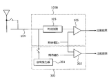
- FIG. 18 is a diagram illustrating an example of the circuit configuration of the auxiliary inspection circuit 300.
- FIG. 18 shows a case where the auxiliary inspection circuit 300 performs the inspection of the second failure inspection circuit 100B. Note that the same configuration can be applied to the auxiliary inspection circuit 300 also when the first failure inspection circuit 100A is inspected.
- the auxiliary inspection circuit 300 includes a signal generator 301 and a comparison circuit 302.
- the signal generator 301 outputs a monitor output signal for checking whether or not the second expected value comparison circuit 106 is operating normally. As shown in FIG. 18, a switch may be inserted between the signal generator 301 and the monitor output signal line 104 so that the monitor output signal line 104 and the signal generator 301 can be electrically disconnected.
- the monitor output signal output from the signal generator 301 may have any signal pattern, for example, a toggle pattern in which High and Low are repeated.
- a monitor output signal is output to the second failure inspection circuit 100B via the source line 11 to be inspected, but the second failure inspection circuit 100B.
- a monitor output signal is directly output from the signal generator 301 to the second failure inspection circuit 100B.
- the monitor output signal from the signal generator 301 is input to the second failure inspection circuit 100B (second determination circuit 105) via the monitor output signal line 104.
- the second determination circuit 105 detects the voltage level of the monitor output signal from the signal generator 301.
- the second expected value comparison circuit 106 compares the output of the second determination circuit 105 with the expected value Em for the monitor output signal.
- the expected value Em is a value indicating the voltage level of the monitor output signal, and is generated by an expected value generation circuit (not shown) that generates expected values E21 and E22 for inspecting the source line 11.
- the comparison result of the second expected value comparison circuit 106 is output to an LCD controller (not shown) or a computer. The LCD controller and the computer execute predetermined processing based on the comparison result.
- the second failure inspection circuit 100B If the second failure inspection circuit 100B is operating normally, a comparison result indicating that the output of the second determination circuit 105 matches the expected value Em for the monitor output signal is output, and the second If failure inspection circuit 100B is not operating normally, a comparison result indicating that they do not match is output. Thereby, it is possible to detect whether or not the second failure inspection circuit 100B is operating normally.
- the cause of the abnormal operation is an abnormality of the second expected value comparison circuit 106 or an abnormality of an expected value generation circuit (not shown) that generates the expected value Em. Can be considered.
- the comparison circuit 302 compares the expected value Em for the monitor output signal with the expected value Er for reference for determining the suitability of the expected value Em.
- the reference expected value Er is a value indicating the voltage level of the monitor output signal, and is generated by an expected value generation circuit (not shown) different from the above-described expected value generation circuit that generates the expected value Em. Similar to the comparison result of the expected value comparison circuit 106, the comparison result of the comparison circuit 302 is output to an LCD controller (not shown) or a computer.
- the expected value Em is a correct value, a comparison result indicating that the monitor output signal expected value Em matches the reference expected value Er is output. If the expected value Em is not the correct value, both A comparison result indicating that the values do not match is output. Accordingly, it is possible to determine whether the expected value Em is appropriate, that is, which of the second expected value comparison circuit 106 and the expected value generation circuit (not shown) that generated the expected value Em is abnormal.
- the auxiliary inspection circuit 300 can determine whether or not the first failure inspection circuit 100A is operating normally.
- auxiliary inspection circuit 300 for inspecting the failure inspection circuit 100 is added to the active matrix substrate 1 according to the first embodiment.
- the active matrix substrate 1 according to the second embodiment An auxiliary inspection circuit 300 can be added to the matrix substrate 1A.
- the first failure inspection circuits 100A and 200A for failure inspection of the gate line 12 and the second failure inspection circuits 100B and 200B for failure inspection of the source line 11 are provided. You may make it have one side.
- the case where the source driver 15, the gate driver 16, and the failure inspection circuits 100 and 200 are mounted on the glass substrate that seals the liquid crystal layer 3 has been described, but the source driver 15, the gate driver 16,
- the failure inspection circuits 100 and 200 may be formed on a circuit board different from the glass substrate and connected to the circuit on the glass substrate.
- the number of sets of the first monitor input signal lines 111 and 203 and the first monitor output signal lines 112 and 204 is not limited to three sets, depending on the standard of the liquid crystal panel P, the required inspection time, etc. It can be designed appropriately. The same applies to the number of second monitor input signal lines 103 and second monitor output signal lines 104.
- the failure inspection of the liquid crystal display device LCD may be performed when the image display is not being performed and the liquid crystal display device LCD is not operated. For example, when the power of the liquid crystal display device LCD is turned on, the video display may be started after performing a failure inspection on all of the source line 11 and the gate line 12.
- a failure inspection mode in which a failure inspection can be performed at any time may be provided. In this case, since the failure location can be easily identified, the inspection process can be facilitated.
- the present invention is useful for a liquid crystal display device having an active matrix type liquid crystal panel.
Landscapes
- Physics & Mathematics (AREA)
- Engineering & Computer Science (AREA)
- General Physics & Mathematics (AREA)
- Nonlinear Science (AREA)
- Chemical & Material Sciences (AREA)
- Crystallography & Structural Chemistry (AREA)
- Computer Hardware Design (AREA)
- Theoretical Computer Science (AREA)
- Optics & Photonics (AREA)
- Mathematical Physics (AREA)
- Microelectronics & Electronic Packaging (AREA)
- Control Of Indicators Other Than Cathode Ray Tubes (AREA)
- Liquid Crystal (AREA)
Abstract
アクティブマトリクス方式の液晶パネルを有する液晶表示装置である。液晶表示装置は、ソース線及びゲート線と、画素電極と、スイッチング素子と、ソースドライバと、ゲートドライバと、故障検査回路と、を有する。ソース線及びゲート線は、格子状に配置される。画素電極は、ソース線及びゲート線によって区画された画素領域に配置される。スイッチング素子は、画素電極に対応して配置される。ソースドライバは、ソース線を駆動する。ゲートドライバは、ゲート線を駆動する。故障検査回路は、ソース線又はゲート線に接続され、ソース線又はゲート線の検査を行う。故障検査回路は、モニタ入力信号線と、モニタ出力信号線と、モニタ出力信号線からの出力信号の電圧レベルを検出する判定回路と、判定回路からの出力と期待値とを比較する期待値比較回路と、を有する。
Description
本発明は、アクティブマトリクス方式の液晶パネルを有する液晶表示装置及びその故障検査方法に関する。
近年、車載用の液晶表示装置は、カーナビゲーション用としてだけでなく、スピードメーター、タコメーター、水温計等の計器類が組み込まれるインストルメントパネルにおいても利用されている。液晶表示装置を適用したインストルメントパネルにおいては、計器類だけでなく、車両に搭載される装置(例えばブレーキやエアバッグ等の車載装置)の異常を報知する警告も、例えば警告アイコンによって液晶表示装置に表示される(図1参照)。図1に示す表示画面D1には、スピードメーターSM、タコメーターTM、及び警告アイコンWI等が表示されている。
このように、インストルメントパネルに液晶表示装置を適用する場合、通常、従来と同様の警告灯WLが表示画面D1に隣接して配置される。これにより、液晶表示装置が故障して、警告アイコンWIが表示されるべき警告表示領域が表示不能となっても、警告灯WLにより車載装置の異常が報知されるので、乗員の安全は確保される(フェールセーフ)。
本発明は、簡易な回路構成により、液晶パネルの故障(ソース線/ゲート線のオープン異常及びショート異常)を自己診断できる液晶表示装置及び故障検査方法を提供する。
本発明の一態様に係る液晶表示装置は、第1の基板、第1の基板に対向して配置される第2の基板、及び第1の基板と第2の基板との間に封止された液晶層を有するアクティブマトリクス方式の液晶パネルを有する液晶表示装置である。液晶表示装置は、ソース線及びゲート線と、画素電極と、スイッチング素子と、ソースドライバと、ゲートドライバと、故障検査回路と、を有する。ソース線及びゲート線は、格子状に配置される。画素電極は、ソース線及びゲート線によって区画された画素領域に配置される。スイッチング素子は、画素電極に対応して配置される。ソースドライバは、ソース線を駆動する。ゲートドライバは、ゲート線を駆動する。故障検査回路は、ソース線又はゲート線に接続され、ソース線又はゲート線の検査を行う。故障検査回路は、モニタ入力信号線と、モニタ出力信号線と、モニタ出力信号線からの出力信号の電圧レベルを検出する判定回路と、判定回路からの出力と期待値とを比較する期待値比較回路と、を有する。
本発明の別の一態様に係る故障検査方法は、上記の液晶表示装置の故障検査方法であって、映像表示期間中に、ゲートドライバからのゲート信号が印加された際の出力信号をもとに、ゲート線の故障検査を行う。
本発明のさらに別の一態様に係る故障検査方法は、上記の液晶表示装置の故障検査方法であって、複数の映像表示期間の間のブランキング期間中に、ソース線の故障検査を行う。
本発明によれば、簡易な回路構成により、液晶パネルの故障を自己診断することができる。
本発明の実施の形態の説明に先立ち、従来の技術における問題点を簡単に説明する。上述したように、従来は、液晶表示装置で車載装置の故障を警告できるにもかかわらず、警告灯も配置するようになっているため、その分、装置コストが増大する。また、液晶表示装置が故障した場合に、その故障が液晶パネル側の故障であるのか、制御部側の故障であるのかを判断するためには、液晶表示装置を分解して、専用の検査装置を用いて検査する必要があり、検査工程が繁雑である。
一方で、アクティブマトリクス方式の液晶パネルにおいては、ドライバIC(integrated circuit)(ソースドライバ及びゲートドライバ)を実装する前に、液晶パネルが正常に動作するか検査するために、画素ごとに点灯検査を行う故障検査回路(以下、「初期不良検査回路」と称する)が表示領域の周辺に設けられている(例えば特許文献1)。しかしながら、この初期不良検査回路は、製造段階での故障検査にのみ用いられ、ドライバICが実装された後、例えば液晶表示装置において映像表示中に利用することはできない。
以下、本発明の実施の形態を、図面を参照して詳細に説明する。
[第1の実施の形態]
図2は、本発明の一実施の形態に係る液晶表示装置(liquid crystal display)LCDの一例を示す図である。液晶表示装置LCDは、例えば、車両のインストルメントパネルに適用され、計器類や車載装置の異常警告の表示を行う。
図2は、本発明の一実施の形態に係る液晶表示装置(liquid crystal display)LCDの一例を示す図である。液晶表示装置LCDは、例えば、車両のインストルメントパネルに適用され、計器類や車載装置の異常警告の表示を行う。
図2に示すように、液晶表示装置LCDは、液晶パネルP及び液晶パネルPの背面側に配置されるバックライトBLを有する。液晶パネルPは、アクティブマトリクス基板1(第1の基板)と、アクティブマトリクス基板1に対向して配置される対向基板2(第2の基板)と、アクティブマトリクス基板1と対向基板2との間に封止される液晶層3と、を有する。アクティブマトリクス基板1と対向基板2は、例えばガラスでできた基板である。アクティブマトリクス基板1の背面側には偏光板4が配置され、対向基板2の表面側には偏光板5が配置される。対向基板2は、対向電極(コモン電極)及びカラーフィルター等を有する(いずれも図示略)。アクティブマトリクス基板1の詳細な構成については後述する。
図3は、第1の実施の形態に係るアクティブマトリクス基板1の回路構成の一例を示す図である。図3に示すように、アクティブマトリクス基板1は、格子状に配置されるソース線11(データ線)及びゲート線12(走査線)と、ソース線11及びゲート線12によって区画された画素領域に配置される画素電極13(サブ画素電極)と、画素電極13に対応して配置されるスイッチング素子14と、ソース線11を駆動するソースドライバ15と、ゲート線12を駆動するゲートドライバ16と、故障検査回路100と、を有する。
本実施の形態におけるアクティブマトリクス基板1は、VGA(Video Graphics Array)パネル(640×480画素)用の基板であり、1920本のソース線11と、480本のゲート線12を有する。ソース線11とゲート線12で区画される画素領域は、RGB(赤、緑、青)ごとのサブ画素領域であり、水平方向(ゲート線方向)に隣接する3つのサブ画素領域により1つの画素領域が構成される。
スイッチング素子14は、ゲート電極、ソース電極及びドレイン電極を有する薄膜トランジスター(TFT:Thin Film Transistor)である。スイッチング素子14のゲート電極はゲート線12に接続され、ソース電極はソース線11に接続され、ドレイン電極は画素電極13の一端に接続される。画素電極13の他端は、液晶層3を介して、対向電極(符号略)に接続される。
ソースドライバ15及びゲートドライバ16は、画素領域の周辺に配置される。ゲートドライバ16は、スイッチング素子14を順にオン状態とするために、ゲート線12にパルス状の電圧を順次印加する。ここでは、図4に示すように、ゲートドライバ16は、2クロック幅で1クロックごとシフトしながら動作する。
ソースドライバ15は、オン状態にあるスイッチング素子14を通じて、液晶層3に印加する電圧を供給する(図5参照)。これにより、オン状態にあるスイッチング素子14に対応する画素が点灯する。
具体的には、ソースドライバ15は、LCDコントローラー(図示略)から受け取った映像信号(デジタルの色データ)をアナログ電圧に変換し、ロード信号LDの立ち上がりのタイミングでソース線11を介して出力する。この電圧はスイッチング素子14を介して画素電極13に印加される。画素電極13に印加される電圧は、ゲート信号の立ち下がりで確定される(図6参照)。液晶層3自体が持つ容量によって、この電圧は次の書込みまで保持される。この電圧によって液晶層3における光の透過率が変化し、透過率に応じた色が表示される。
図6に示すように、あるフレームの表示期間と、次のフレームの表示期間の間には、ブランキング期間(垂直帰線期間)がある。ブランキング期間中はゲート信号がオフ(OFF)のため、ソースドライバ出力が変動しても表示に影響を与えない。
本実施の形態では、このブランキング期間を利用して、ソース線11の故障検査が行われる。なお、一回のブランキング期間にソース線11の全部について故障検査を行うことが困難である場合、所定の間隔で間引くことにより、全体的に表示領域を検査するのが好ましい。また、ゲート線12の故障検査は、映像表示中に行うことができる。
故障検査回路100は、所定の配線パターンL1、L2(図7、図9参照)、配線パターンL1、L2からの出力信号の電圧レベルを検出する判定回路114、105、及び判定回路114、105からの出力と期待値とを比較する期待値比較回路115、106を有する。故障検査回路100は、ソースドライバ15又はゲートドライバ16を利用して、ソース線11又はゲート線12の検査を行う。期待値比較回路115、106の比較結果は、LCDコントローラー(図示略)や、コンピューターに出力される。LCDコントローラーやコンピューターは、比較結果に基づいて、所定の処理を実行する。
本実施の形態では、故障検査回路100は、ゲート線12の検査を行う第1の故障検査回路100A(図7参照)及びソース線11の検査を行う第2の故障検査回路100B(図9参照)を含む。
図7は、ゲート線12のオープン異常(断線)及びショート異常(短絡)を検査するための回路構成の一例を示す図である。図7に示すように、第1の故障検査回路100Aは、第1の配線パターンL1、第1の判定回路114及び第1の期待値比較回路115を有する。第1の判定回路114及び第1の期待値比較回路115のうち少なくとも1方は、ゲートドライバ16に組み込まれてもよい。
第1の配線パターンL1は、第1のモニタ入力信号線111、第1のモニタ出力信号線112、及び第1のスイッチング素子113を有する。第1のモニタ入力信号線111は、ゲート線12の検査用の第1のモニタ入力信号Gin(Gin1~Gin3)を入力する。第1のモニタ出力信号線112は、第1のモニタ入力信号Ginに基づく第1のモニタ出力信号Gout(Gout1~Gout3)を、第1の判定回路114に対して出力する。第1のスイッチング素子113は、ゲート電極、ソース電極及びドレイン電極を有するトランジスターである。第1のスイッチング素子113のゲート電極はゲート線12におけるゲートドライバ16の反対側に接続され、ドレイン電極は第1のモニタ入力信号線111に接続され、ソース電極はモニタ出力信号線112に接続される。
図8は、ゲート線の故障検査結果の一例を示すタイミングチャートである。図8に示す第1のモニタ出力信号Goutが、第1の判定回路114に入力される電圧レベルである。第1の期待値比較回路115は、ゲート線12が正常であるときに得られるべき電圧レベルを第1の期待値E1として、第1の判定回路114で検出された電圧レベルと第1の期待値E1を比較することにより、ゲート線12のオープン異常及びショート異常を判断する。なお、ゲート線12の故障検査は、例えば映像表示中のゲート線12の駆動動作を利用して行われる。
図8に示すように、ゲート信号G1~G480は、2クロック幅で1クロックごとシフトしながら動作する。ゲート信号Gが入力されているゲート線12が検査対象となる。すなわち、ゲート線12がゲート電極に接続されている第1のスイッチング素子113がオン状態となり、このオン状態にある第1のスイッチング素子113に接続されている第1のモニタ入力信号線111から1クロック幅で第1のモニタ入力信号Ginが入力される。第1のモニタ入力信号線111からの第1のモニタ入力信号Ginに応じた第1のモニタ出力信号Goutが、第1のモニタ出力信号線112を介して第1の判定回路114に出力される。
図8に示すように、検査対象のゲート線12にショート異常及びオープン異常がなければ、第1のモニタ入力信号Ginが入力され、第1のモニタ入力信号Ginの電圧レベルが“ハイ”(“HIGH”)になることに伴い、対応する第1のモニタ出力信号Goutの電圧レベルも“HIGH”になる。第1のモニタ出力信号Goutの電圧レベルは、次のゲート信号Gが入力されるまで保持される。例えば、ゲート信号G1が入力されているとき、第1のモニタ入力信号線111に第1のモニタ入力信号Gin1が入力されると、第1のモニタ出力信号Gout1の電圧レベルは“HIGH”になる。そして、次のゲート信号G4が入力されたとき、この時点で第1のモニタ入力信号Gin1の電圧レベルは“ロー”“LOW”なので、第1のモニタ出力信号Gout1の電圧レベルは“LOW”になる。
一方、ゲート線12にオープン異常が生じている場合、ゲート線12を通じてゲート信号Gが入力されても第1のスイッチング素子113はオン状態とならない。したがって、第1のモニタ入力信号Ginが入力されても、第1のモニタ出力信号Goutの電圧レベルは“LOW”のままとなる。これにより、第1の期待値比較回路115は、ゲート線12のオープン異常を検出することができる。
また、ゲート線12にショート異常が生じている場合、第1のモニタ出力信号Goutの電圧レベルが“HIGH”で保持されるべき期間に、電圧レベルが低下する。例えば、図8に示すように、ゲート信号G1の電圧レベルが“LOW”になると、第1のスイッチング素子113はオフ状態となり、第1のモニタ出力信号Gout1の電圧レベルは“HIGH”で保持されるべきである。しかし、ゲート信号G1が入力されるゲート線12と隣接するゲート信号G2が入力されるゲート線12が短絡している場合、2本のゲート線12の電圧レベルは、各ゲート線12に入力された電圧レベルの間の値となる。よって、ゲート信号G2の入力により、第1のモニタ出力信号Gout1を出力する第1のスイッチング素子113も“HIGH”と“LOW”の間の電圧レベルとなり、その結果、第1のスイッチング素子113はオフ状態ではなく不定状態となる。このとき、第1のモニタ入力信号Gin1は入力されていないので、第1のモニタ出力信号Gout1の電圧レベルが低下する。これにより、第1の期待値比較回路115は、ゲート線12のショート異常を検出することができる。
図9は、ソース線11のオープン異常(断線)及びショート異常(短絡)を検査するための回路構成の一例を示す図である。図9に示すように、第2の故障検査回路100Bは、第2の配線パターンL2、第2の判定回路105及び第2の期待値比較回路106を有する。第2の判定回路105及び第2の期待値比較回路106のうち少なくとも1方は、ソースドライバ15に組み込まれてもよい。
第2の配線パターンL2は、第2のモニタ入力信号線103、第2のモニタ出力信号線104、第2のスイッチング素子102、及び制御信号線101を有する。第2のモニタ入力信号線103は、ソース線11の検査用の第2のモニタ入力信号DRGB(DR1、DR2、DG1、DG2、DB1、DB2)を入力する。第2のモニタ出力信号線104は、第2のモニタ入力信号DRGBに基づく第2のモニタ出力信号Sout(Sout1、Sout2)又はソースドライバ15からの入力信号に基づく第2のモニタ出力信号Soutを、第2の判定回路105に対して出力する。第2のスイッチング素子102は、ゲート電極、ソース電極及びドレイン電極を有するトランジスターである。第2のスイッチング素子102のゲート電極は制御信号線101に接続され、ドレイン電極は第2のモニタ入力信号線103に接続され、ソース電極はソース線11におけるソースドライバ15の反対側に接続される。ソースドライバ15に設けられたスイッチSWにより、第2のモニタ入力信号DRGBに基づく第2のモニタ出力信号Sout又はソースドライバ15からの入力信号に基づく第2のモニタ出力信号Soutが、第2の判定回路105に対して選択的に出力される。
図10は、ソース線11のショート異常を検出する場合の動作の一例を示す図である。図11は、ソース線11の故障検査結果(ショート異常)の一例を示すタイミングチャートである。図11に示すモニタ出力信号が、第2の判定回路105に入力される電圧レベルである。第2の期待値比較回路106は、ソース線11が正常であるときに得られるべき電圧レベルを第2の期待値E21として、第2の判定回路105で検出された電圧レベルと第2の期待値E21を比較することにより、ソース線11のショート異常を判断する。なお、ソース線11のショート異常の検査は、例えば映像表示中のブランキング期間の前半に行われる。
図10に示すように、制御信号線101からの制御信号TRの電圧レベルは“LOW”に設定される。したがって、第2のスイッチング素子102はオフ状態となる。この状態で、検査対象となるソース線11に対応するソースドライバ15から第2のモニタ出力信号線104に向けて入力信号が入力される。ソースドライバ15からの入力信号に応じた第2のモニタ出力信号Soutが、第2のモニタ出力信号線104を介して第2の判定回路105に出力される。
図11に示すように、検査対象のソース線11にショート異常及びオープン異常がない場合、ソースドライバ15から入力信号が入力されると、第2のモニタ出力信号Soutの電圧レベルもソースドライバ15からの入力信号に応じた値となる。図11に示す例の場合、奇数番目のソース電極に対応する第2のモニタ出力信号Soutの電圧レベルは“HIGH”になる。
一方、ソース線11にショート異常が生じている場合、第2のモニタ出力信号線104に所望の電圧が印加されないので、第2のモニタ出力信号Soutの電圧レベルが所定の規格範囲(規格上限値~規格下限値)外となる。これにより、第2の期待値比較回路106は、ソース線11のショート異常を検出することができる。
図12は、ソース線11のオープン異常を検出する場合の動作の一例を示す図である。図13は、ソース線11の故障検査結果(オープン異常)の一例を示すタイミングチャートである。図13に示すモニタ出力信号が、第2の判定回路105で検出される電圧レベルである。第2の期待値比較回路106は、ソース線11が正常であるときに得られるべき電圧レベルを第2の期待値E22として、第2の判定回路105で検出された電圧レベルと第2の期待値E22を比較することにより、ソース線11のオープン異常を判断する。なお、ソース線11のオープン異常の検査は、例えば映像表示中のブランキング期間の後半に行われる。
図12に示すように、制御信号線101からの制御信号TRの電圧レベルは“HIGH”に設定される。したがって、第2のスイッチング素子102はオン状態となる。また、ソースドライバ15のスイッチSWにより、検査対象のソース線11が第2のモニタ出力信号線104に接続される。この状態で、検査対象となるソース線11に接続された第2のモニタ入力信号線103から第2のモニタ入力信号DRGBが入力される。第2のモニタ入力信号DRGBの電圧レベルは、アナロググランド端子の電圧レベルAVSSに固定される。第2のモニタ入力信号DRGBに基づく第2のモニタ出力信号Soutが、第2のモニタ出力信号線104を介して第2の判定回路105に出力される。
図13に示すように、検査対象のソース線11にオープン異常がない場合、第2のモニタ入力信号DRGBが入力されると、第2のモニタ出力信号Soutの電圧レベルは、モニタ入力信号DRGBの電圧レベルAVSSと同等になる。
一方、ソース線11にオープン異常が生じている場合、第2のモニタ出力信号線104に所望の電圧が印加されないので、第2のモニタ出力信号Soutの電圧レベルが所定の規格範囲(規格上限値~規格下限値)外となる。これにより、第2の期待値比較回路106は、ソース線11のオープン異常を検出することができる。
なお、本実施の形態では、ソース線11のうちのS1とS2に接続されるスイッチSWを一度にオン状態とし、一度に2本のソース線11の検査を行っている。以降、オンとなるスイッチSWを順に切り換えることにより、全ソース線11の検査が行われる。一回のブランキング期間で全ソース線11の検査が完了しない場合、次回以降のブランキング期間で残りのソース線11の検査を行う。なお、一度に検査するソース線の数は、配線数に応じて変化する。
このように、第1の実施の形態に係る液晶表示装置LCDは、アクティブマトリクス基板1(第1の基板)、アクティブマトリクス基板1に対向して配置される対向基板2(第2の基板)、及びアクティブマトリクス基板1と対向基板2との間に封止された液晶層3を有するアクティブマトリクス方式の液晶パネルPを有する。液晶表示装置LCDは、ソース線11及びゲート線12と、画素電極13と、スイッチング素子14と、ソースドライバ15と、ゲートドライバ16と、故障検査回路100と、を有する。ソース線11及びゲート線12は、格子状に配置される。画素電極13は、ソース線11及びゲート線12によって区画された画素領域に配置される。スイッチング素子14は、画素電極13に対応して配置される。ソースドライバ15は、ソース線11を駆動する。ゲートドライバ16は、ゲート線12を駆動する。故障検査回路100は、ソース線11又はゲート線12に接続され、ソース線11又はゲート線12の検査を行う。故障検査回路100は、モニタ入力信号線111、103と、モニタ出力信号線112、104と、モニタ出力信号線112、104からの出力信号の電圧レベルを検出する判定回路114、105と、判定回路114、105からの出力と期待値E1、E2とを比較する期待値比較回路115、106と、を有する。
液晶表示装置LCDによれば、簡易な回路構成により、液晶パネルPの故障を自己診断することができる。液晶表示装置LCDを車載用として適用する場合、ソース線11又はゲート線12の異常により、警告表示領域が表示不能となった場合に、正常な表示領域に警告表示を行う等、液晶表示装置LCDが自己診断に基づいて故障を回避できるように動作することで、フェールセーフ機能が実現される。したがって、警告灯を配置する必要がなくなり、装置コストを低減することができる。
[第2の実施の形態]
第2の実施の形態では、液晶表示装置LCDのアクティブマトリクス基板として、第1の実施の形態に係るアクティブマトリクス基板1に代えて、故障検査回路の構成が異なるアクティブマトリクス基板1Aを適用している。
第2の実施の形態では、液晶表示装置LCDのアクティブマトリクス基板として、第1の実施の形態に係るアクティブマトリクス基板1に代えて、故障検査回路の構成が異なるアクティブマトリクス基板1Aを適用している。
図14は、第2の実施の形態に係るアクティブマトリクス基板1Aの回路構成の一例を示す図である。図14に示すように、アクティブマトリクス基板1Aは、第1の実施の形態に係るアクティブマトリクス基板1と同様に、ソース線11(データ線)及びゲート線12(走査線)と、画素電極13(サブ画素電極)と、スイッチング素子14と、ソースドライバ15と、ゲートドライバ16と、故障検査回路200と、を有する。ソース線11(データ線)及びゲート線12(走査線)は、格子状に配置される。画素電極13(サブ画素電極)は、ソース線11及びゲート線12によって区画された画素領域に配置される。スイッチング素子14は、画素電極13に対応して配置される。ソースドライバ15は、ソース線11を駆動する。ゲートドライバ16は、ゲート線12を駆動する。故障検査回路200以外の構成は、第1の実施の形態に係るアクティブマトリクス基板1の構成と同様であるので説明を省略する。
故障検査回路200は、所定の配線パターンL2、L3、配線パターンL2、L3からの出力信号の電圧レベルを検出する判定回路105、205、及び判定回路105、205からの出力と期待値とを比較する期待値比較回路106、206を有する。故障検査回路200は、ソースドライバ15又はゲートドライバ16を利用して、ソース線11又はゲート線12の検査を行う。期待値比較回路106、206の比較結果は、LCDコントローラー(図示略)や、コンピューターに出力される。LCDコントローラーやコンピューターは、比較結果に基づいて、所定の処理を実行する。
本実施の形態では、故障検査回路200は、ゲート線12の検査を行う第1の故障検査回路200A及びソース線11の検査を行う第2の故障検査回路200Bを含む。第2の故障検査回路200Bは、第1の実施の形態における第2の故障検査回路100Bと同様であるので、説明を省略する。なお、本実施の形態では、第1の故障検査回路200Aによるゲート線12のショート異常検査は、映像表示期間中に行われ、第1の故障検査回路200Aによるゲート線12のオープン異常検査は、例えば電源投入時などの映像表示期間外に行われ、第2の故障検査回路200Bによるソース線11の故障検査は、複数の映像表示期間の間のブランキング期間を利用して行われる。
図14に示すように、第1の故障検査回路200Aは、第1の配線パターンL3、第1の判定回路205及び第1の期待値比較回路206を有する。第1の判定回路205及び第1の期待値比較回路206のうち少なくとも1方は、ゲートドライバ16に組み込まれてもよい。
第1の配線パターンL3は、第1のモニタ入力信号線203、第1のモニタ出力信号線204、第1のスイッチング素子202、及び制御信号線201を有する。第1のモニタ入力信号線203は、ゲート線12の検査用の第1のモニタ入力信号Gin(Gin1~Gin3)を入力する。第1のモニタ出力信号線204は、第1のモニタ入力信号Ginに基づく第1のモニタ出力信号Gout(Gout1~Gout3)又はゲートドライバ16からの入力信号に基づく第1のモニタ出力信号Goutを、第1の判定回路205に対して出力する。第1のスイッチング素子202は、ゲート電極、ソース電極及びドレイン電極を有するトランジスターである。第1のスイッチング素子202のゲート電極は制御信号線201に接続され、ドレイン電極は第1のモニタ入力信号線203に接続され、ソース電極はゲート線12におけるゲートドライバ16の反対側に接続される。ゲートドライバ16に設けられたスイッチSWにより、第1のモニタ入力信号Ginに基づく第1のモニタ出力信号Gout又はゲートドライバ16からの入力信号に基づく第1のモニタ出力信号Goutが、第1の判定回路205に対して選択的に出力される。
図15は、ゲート線12のショート異常を検出する場合の動作の一例を示す図である。第1の期待値比較回路206は、ゲート線12が正常であるときに得られるべき電圧レベルを第1の期待値E11として、第1の判定回路205で検出された電圧レベルと第1の期待値E11を比較することにより、ゲート線12のショート異常を判断する。なお、ゲート線12のショート異常の検査は、例えば映像表示中のゲート線12の駆動動作を利用して行われる。
図15に示すように、制御信号線201からの制御信号TRの電圧レベルは“LOW”に設定される。したがって、第1のスイッチング素子202はオフ状態となる。この状態で、検査対象となるゲート線12に対応するゲートドライバ16から第1のモニタ出力信号線204に向けて入力信号が入力される。ゲートドライバ16からの入力信号に応じた第1のモニタ出力信号Goutが、第1のモニタ出力信号線204を介して第1の判定回路205に出力される。
検査対象のゲート線12にショート異常がない場合、ゲートドライバ16から入力信号が入力されると、第1のモニタ出力信号Goutの電圧レベルもゲートドライバ16からの入力信号に応じた値となる。
一方、ゲート線12にショート異常が生じている場合、第1のモニタ出力信号線204に所望の電圧が印加されないので、第1のモニタ出力信号Goutの電圧レベルが所定の規格範囲(規格上限値~規格下限値)外となる。これにより、第1の期待値比較回路206は、ゲート線12のショート異常を検出することができる。
図16は、ゲート線12のオープン異常を検出する場合の動作の一例を示す図である。第1の期待値比較回路206は、ゲート線12が正常であるときに得られるべき電圧レベルを第1の期待値E12として、第1の判定回路205で検出された電圧レベルと第1の期待値E12を比較することにより、ゲート線12のオープン異常を判断する。なお、ゲート線12のオープン異常の検査は、例えば電源投入時など映像表示期間外に行われる。
図16に示すように、制御信号線201からの制御信号TRの電圧レベルは“HIGH”に設定される。したがって、第1のスイッチング素子202はオン状態となる。また、ゲートドライバ16のスイッチSWにより、検査対象のゲート線12が第1のモニタ出力信号線204に接続される。この状態で、検査対象となるゲート線12に接続された第1のモニタ入力信号線203から第1のモニタ入力信号Ginが入力される。第1のモニタ入力信号Ginに基づく第1のモニタ出力信号Goutが、第1のモニタ出力信号線204を介して第1の判定回路205に出力される。
検査対象のゲート線12にオープン異常がない場合、第1のモニタ入力信号Ginが入力されると、第1のモニタ出力信号Goutの電圧レベルは、モニタ入力信号Ginの電圧レベルと同等になる。
一方、ゲート線12にオープン異常が生じている場合、第1のモニタ出力信号線204に所望の電圧が印加されないので、第1のモニタ出力信号Goutの電圧レベルが所定の規格範囲(規格上限値~規格下限値)外となる。これにより、第1の期待値比較回路206は、ゲート線12のオープン異常を検出することができる。
なお、本実施の形態では、ゲート線12のうちのG1~G3に接続されるスイッチSWを一度にオン状態とし、一度に3本のゲート線12の検査を行っている。以降、オンとなるスイッチSWを順に切り換えることにより、全ゲート線12の検査が行われる。なお、一度に検査するゲート線12の数は、配線数に応じて変化する。
このように、第2の実施の形態に係る液晶表示装置LCDは、アクティブマトリクス基板1A(第1の基板)、アクティブマトリクス基板1Aに対向して配置される対向基板2(第2の基板)、及びアクティブマトリクス基板1Aと対向基板2との間に封止された液晶層3を有するアクティブマトリクス方式の液晶パネルPを有する。液晶表示装置LCDは、ソース線11及びゲート線12と、画素電極13と、スイッチング素子14と、ソースドライバ15と、ゲートドライバ16と、故障検査回路200と、を有する。ソース線11及びゲート線12は、格子状に配置される。画素電極13は、ソース線11及びゲート線12によって区画された画素領域に配置される。スイッチング素子14は、画素電極13に対応して配置される。ソースドライバ15は、ソース線11を駆動する。ゲートドライバ16は、ゲート線12を駆動する。故障検査回路200は、ソース線11又はゲート線12に接続され、ソース線11又はゲート線12の検査を行う。故障検査回路200は、モニタ入力信号線203、103と、モニタ出力信号線204、104と、モニタ出力信号線204、104からの出力信号の電圧レベルを検出する判定回路205、105と、判定回路205、105からの出力と期待値E1、E2とを比較する期待値比較回路206、106と、を有する。
第2の実施の形態に係る液晶表示装置LCDによれば、第1の実施の形態と同様に、簡易な回路構成により、液晶パネルPの故障を自己診断することができる。液晶表示装置LCDを車載用として適用する場合、ソース線11又はゲート線12の異常により、警告表示領域が表示不能となった場合に、正常な表示領域に警告表示を行う等、液晶表示装置LCDが自己診断に基づいて故障を回避できるように動作することで、フェールセーフ機能が実現される。したがって、警告灯を配置する必要がなくなり、装置コストを低減することができる。
[第3の実施の形態]
図17は、第3の実施の形態に係るアクティブマトリクス基板1Bの回路構成の一例を示す図である。図17に示すアクティブマトリクス基板1Bは、第1の実施の形態に係るアクティブマトリクス基板1に、故障検査回路100の検査を行う補助検査回路300を追加したものである。
図17は、第3の実施の形態に係るアクティブマトリクス基板1Bの回路構成の一例を示す図である。図17に示すアクティブマトリクス基板1Bは、第1の実施の形態に係るアクティブマトリクス基板1に、故障検査回路100の検査を行う補助検査回路300を追加したものである。
補助検査回路300は、ゲート線12の検査を行う第1の故障検査回路100A(第1の判定回路114、第1の期待値比較回路115)及びソース線11の検査を行う第2の故障検査回路100B(第2の判定回路105、第2の期待値比較回路106)のそれぞれに接続される。補助検査回路300を設けることにより、故障検査回路100自体の検査を行うことが可能となるので、液晶表示装置LCDの故障検出の信頼性が向上する。
図18は、補助検査回路300の回路構成の一例を示す図である。図18では、補助検査回路300が、第2の故障検査回路100Bの検査を行う場合について示している。なお、第1の故障検査回路100Aの検査を行う場合も、補助検査回路300には同様の構成を適用できる。
図18に示すように、補助検査回路300は、信号発生器301及び比較回路302を有する。
信号発生器301は、第2の期待値比較回路106が正常に動作しているか否かを検査するためのモニタ出力信号を出力する。図18に示すように、信号発生器301とモニタ出力信号線104との間にスイッチを挿入して、モニタ出力信号線104と信号発生器301を電気的に切断可能に構成してもよい。信号発生器301から出力されるモニタ出力信号は、いかなる信号パターンでもよく、例えば、HighとLowを繰返すトグルパターンであってもよい。
通常の故障検査(ソース線11の検査)では、第2の故障検査回路100Bに対して、検査対象であるソース線11を介してモニタ出力信号が出力されるが、第2の故障検査回路100Bの検査においては、信号発生器301から第2の故障検査回路100Bに対して、直接モニタ出力信号が出力される。信号発生器301からのモニタ出力信号は、モニタ出力信号線104を介して第2の故障検査回路100B(第2の判定回路105)に入力される。
第2の判定回路105は、信号発生器301からのモニタ出力信号の電圧レベルを検出する。第2の期待値比較回路106は、第2の判定回路105の出力とモニタ出力信号用の期待値Emを比較する。期待値Emは、モニタ出力信号の電圧レベルを示す値であり、ソース線11の検査を行うための期待値E21、E22を生成する期待値生成回路(図示略)によって生成される。第2の期待値比較回路106の比較結果は、LCDコントローラー(図示略)や、コンピューターに出力される。LCDコントローラーやコンピューターは、比較結果に基づいて、所定の処理を実行する。
第2の故障検査回路100Bが正常に動作していれば、第2の判定回路105の出力とモニタ出力信号用の期待値Emが一致していることを示す比較結果が出力され、第2の故障検査回路100Bが正常に動作していなければ、両者が一致していないことを示す比較結果が出力される。これにより、第2の故障検査回路100Bが正常に動作しているか否かを検出することができる。
第2の故障検査回路100Bの異常動作が検出された場合、異常動作の要因としては、第2の期待値比較回路106の異常又は期待値Emを生成した期待値生成回路(図示略)の異常が考えられる。
比較回路302は、モニタ出力信号用の期待値Emと、期待値Emの適否を判定するためのリファレンス用の期待値Erを比較する。リファレンス用の期待値Erは、モニタ出力信号の電圧レベルを示す値であり、期待値Emを生成する前述の期待値生成回路とは別の期待値生成回路(図示略)によって生成される。比較回路302の比較結果は、期待値比較回路106の比較結果と同様に、LCDコントローラー(図示略)や、コンピューターに出力される。
期待値Emが正しい値であれば、モニタ出力信号用の期待値Emとリファレンス用の期待値Erが一致していることを示す比較結果が出力され、期待値Emが正しい値でなければ、両者が一致していないことを示す比較結果が出力される。これにより、期待値Emの適否、すなわち、第2の期待値比較回路106と期待値Emを生成した期待値生成回路(図示略)のいずれに異常があるかを判断することができる。
同様にして、補助検査回路300により、第1の故障検査回路100Aが正常に動作しているか否かを判断することもできる。
本実施の形態では、第1の実施の形態に係るアクティブマトリクス基板1に、故障検査回路100の検査を行う補助検査回路300を追加した例について示したが、第2の実施の形態に係るアクティブマトリクス基板1Aに、補助検査回路300を追加することもできる。
以上、本発明者によってなされた発明を実施の形態に基づいて具体的に説明したが、本発明は上記実施の形態に限定されるものではなく、その要旨を逸脱しない範囲で変更可能である。
例えば、実施の形態では、ゲート線12の故障検査用の第1の故障検査回路100A、200Aと、ソース線11の故障検査用の第2の故障検査回路100B、200Bとを有するが、何れか一方を有するようにしてもよい。実施の形態では、ソースドライバ15、ゲートドライバ16、及び故障検査回路100、200が、液晶層3を封止するガラス基板上に実装された場合について説明したが、ソースドライバ15、ゲートドライバ16、及び故障検査回路100、200は、ガラス基板とは別の回路基板上に形成され、ガラス基板上の回路と接続された構成としてもよい。
また例えば、第1のモニタ入力信号線111、203と第1のモニタ出力信号線112、204の組数は3組に限定されず、液晶パネルPの規格や、所要検査時間等に応じて、適宜に設計することができる。第2のモニタ入力信号線103及び第2のモニタ出力信号線104の本数も同様である。
また、液晶表示装置LCDの故障検査は、映像表示中でなく、液晶表示装置LCDを動作させていないときに行われてもよい。例えば、液晶表示装置LCDの電源投入時に、ソース線11及びゲート線12の全部について故障検査を行った後、映像表示を開始するようにしてもよい。また例えば、液晶表示装置LCDが故障した場合に有して、いつでも故障検査を実行できる故障検査モードを有するようにしてもよい。この場合、容易に故障箇所を特定することができるので、検査工程を容易化することができる。
今回開示された実施の形態はすべての点で例示であって制限的なものではないと考えられるべきである。本発明の範囲は上記した説明ではなくて請求の範囲によって示され、請求の範囲と均等の意味および範囲内でのすべての変更が含まれることが意図される。
本発明は、アクティブマトリクス方式の液晶パネルを有する液晶表示装置に有用である。
1,1A,1B アクティブマトリクス基板(第1の基板)
2 対向基板(第2の基板)
3 液晶層
4,5 偏光板
11 ソース線
12 ゲート線
13 画素電極
14 スイッチング素子
15 ソースドライバ
16 ゲートドライバ
100,200 故障検査回路
100A,200A 故障検査回路(第1の故障検査回路)
100B,200B 故障検査回路(第2の故障検査回路)
101,201 制御信号線
102 スイッチング素子(第2のスイッチング素子)
103 モニタ入力信号線(第2のモニタ入力信号線)
104 モニタ出力信号線(第2のモニタ出力信号線)
105 判定回路(第2の判定回路)
106 期待値比較回路(第2の期待値比較回路)
111,203 モニタ入力信号線(第1のモニタ入力信号線)
112,204 モニタ出力信号線(第1のモニタ出力信号線)
113,202 スイッチング素子(第1のスイッチング素子)
114,205 判定回路(第1の判定回路)
115,206 期待値比較回路(第1の期待値比較回路)
300 補助検査回路
301 信号発生器
302 比較回路
Gin モニタ入力信号(第1のモニタ入力信号)
Gout モニタ出力信号(第1のモニタ出力信号)
LCD 液晶表示装置
L1 配線パターン(第1の配線パターン)
L2 配線パターン(第2の配線パターン)
L3 配線パターン(第1の配線パターン)
P 液晶パネル
BL バックライト
SW スイッチ
DRGB モニタ入力信号(第2のモニタ入力信号)
Sout,Sout1,Sout2 モニタ出力信号(第2のモニタ出力信号)
D1 表示画面
SM スピードメーター
TM タコメーター
WI 警告アイコン
WL 警告灯
2 対向基板(第2の基板)
3 液晶層
4,5 偏光板
11 ソース線
12 ゲート線
13 画素電極
14 スイッチング素子
15 ソースドライバ
16 ゲートドライバ
100,200 故障検査回路
100A,200A 故障検査回路(第1の故障検査回路)
100B,200B 故障検査回路(第2の故障検査回路)
101,201 制御信号線
102 スイッチング素子(第2のスイッチング素子)
103 モニタ入力信号線(第2のモニタ入力信号線)
104 モニタ出力信号線(第2のモニタ出力信号線)
105 判定回路(第2の判定回路)
106 期待値比較回路(第2の期待値比較回路)
111,203 モニタ入力信号線(第1のモニタ入力信号線)
112,204 モニタ出力信号線(第1のモニタ出力信号線)
113,202 スイッチング素子(第1のスイッチング素子)
114,205 判定回路(第1の判定回路)
115,206 期待値比較回路(第1の期待値比較回路)
300 補助検査回路
301 信号発生器
302 比較回路
Gin モニタ入力信号(第1のモニタ入力信号)
Gout モニタ出力信号(第1のモニタ出力信号)
LCD 液晶表示装置
L1 配線パターン(第1の配線パターン)
L2 配線パターン(第2の配線パターン)
L3 配線パターン(第1の配線パターン)
P 液晶パネル
BL バックライト
SW スイッチ
DRGB モニタ入力信号(第2のモニタ入力信号)
Sout,Sout1,Sout2 モニタ出力信号(第2のモニタ出力信号)
D1 表示画面
SM スピードメーター
TM タコメーター
WI 警告アイコン
WL 警告灯
Claims (13)
- 第1の基板、前記第1の基板に対向して配置される第2の基板、及び前記第1の基板と前記第2の基板との間に封止された液晶層を有するアクティブマトリクス方式の液晶パネルを備える液晶表示装置であって、
格子状に配置されるソース線及びゲート線と、
前記ソース線及び前記ゲート線によって区画された画素領域に配置される画素電極と、
前記画素電極に対応して配置されるスイッチング素子と、
前記ソース線を駆動するソースドライバと、
前記ゲート線を駆動するゲートドライバと、
前記ソース線又は前記ゲート線に接続され、前記ソース線又は前記ゲート線の検査を行う故障検査回路と、を備え、
前記故障検査回路は、
モニタ入力信号線と、
モニタ出力信号線と、
前記モニタ出力信号線からの出力信号の電圧レベルを検出する判定回路と、
前記判定回路からの出力と期待値とを比較する期待値比較回路と、
を有する液晶表示装置。 - 前記故障検査回路は、
前記ゲート線の検査を行う第1の故障検査回路を含み、
前記第1の故障検査回路は、
前記ゲート線の検査用の第1のモニタ入力信号を入力する第1のモニタ入力信号線と、
前記第1のモニタ入力信号に基づく第1のモニタ出力信号を前記出力信号として出力する第1のモニタ出力信号線と、
前記第1のモニタ出力信号線からの出力信号の電圧レベルを検出する第1の判定回路と、
前記第1の判定回路からの出力と第1の期待値とを比較する第1の期待値比較回路と、
ゲート電極が前記ゲート線に接続され、ドレイン電極及びソース電極の一方が前記第1のモニタ入力信号線に接続され、前記ドレイン電極及び前記ソース電極の他方が前記第1のモニタ出力信号線に接続される第1のスイッチング素子と、
を有する請求項1に記載の液晶表示装置。 - 前記故障検査回路は、
前記ゲート線の検査を行う第1の故障検査回路を含み、
前記第1の故障検査回路は、
前記ゲート線の検査用の第1のモニタ入力信号を入力する第1のモニタ入力信号線と、
前記第1のモニタ入力信号に基づく第1のモニタ出力信号又は前記ゲートドライバからの入力信号に基づく第1のモニタ入力信号を前記出力信号として出力する第1のモニタ出力信号線と、
前記第1のモニタ出力信号線からの出力信号の電圧レベルを検出する第1の判定回路と、
前記第1の判定回路からの出力と第1の期待値とを比較する第1の期待値比較回路と、
ドレイン電極およびソース電極の一方が前記第1のモニタ入力信号線に接続され、前記ドレイン電極および前記ソース電極の他方が前記ゲート線に接続される第1のスイッチング素子と、
前記第1のスイッチング素子のゲート電極に接続され、前記第1のスイッチング素子のオン/オフを切り替える制御信号線と、
を有する請求項1に記載の液晶表示装置。 - 前記第1の判定回路及び前記第1の期待値比較回路のうち少なくとも1方は、前記ゲートドライバに組み込まれる請求項2又は3に記載の液晶表示装置。
- 前記故障検査回路は、
前記ソース線の検査を行う第2の故障検査回路を含み、
前記第2の故障検査回路は、
前記ソース線の検査用の第2のモニタ入力信号を入力する第2のモニタ入力信号線と、
前記第2のモニタ入力信号に基づく第2のモニタ出力信号又は前記ソースドライバからの入力信号に基づく第2のモニタ出力信号を前記出力信号として出力する第2のモニタ出力信号線と、
前記第2のモニタ出力信号線からの出力信号の電圧レベルを検出する第2の判定回路と、
前記第2の判定回路からの出力と第2の期待値とを比較する第2の期待値比較回路と、
ドレイン電極およびソース電極の一方が前記第2のモニタ入力信号線に接続され、前記ドレイン電極および前記ソース電極の他方が前記ソース線に接続される第2のスイッチング素子と、
前記第2のスイッチング素子のゲート電極に接続され、前記第2のスイッチング素子のオン/オフを切り替える制御信号線と、
を有する請求項1から4のいずれか一項に記載の液晶表示装置。 - 前記第2の判定回路及び前記第2の期待値比較回路のうち少なくとも1方は、前記ソースドライバに組み込まれる請求項5に記載の液晶表示装置。
- 前記故障検査回路の検査を行う補助検査回路を有する請求項1から6のいずれか一項に記載の液晶表示装置。
- 前記補助検査回路は、前記故障検査回路に対してモニタ出力信号を出力する信号生成器を有し、
前記判定回路は、前記モニタ出力信号の電圧レベルを検出し、
前記期待値比較回路は、前記判定回路からの出力と前記モニタ出力信号用の期待値とを比較する請求項7に記載の液晶表示装置。 - 前記補助検査回路は、前記モニタ出力信号用の前記期待値と、前記モニタ出力信号用の前記期待値の適否を判定するためのリファレンス用の期待値とを比較する比較回路を有する請求項8に記載の液晶表示装置。
- 前記ソースドライバ、前記ゲートドライバ、および前記故障検査回路は、前記第1の基板、又は前記第2の基板上に実装される請求項1から9のいずれか一項に記載の液晶表示装置。
- 請求項1から10のいずれか一項に記載の液晶表示装置の故障検査方法であって、
映像表示期間中に、前記ゲートドライバからのゲート信号が印加された際の前記出力信号をもとに、前記ゲート線の故障検査を行う故障検査方法。 - 請求項1から10のいずれか一項に記載の液晶表示装置の故障検査方法であって、
複数の映像表示期間の間のブランキング期間中に、前記ソース線の故障検査を行う故障検査方法。 - 請求項3に記載の液晶表示装置の故障検査方法であって、
映像表示期間外に、前記ゲート線のオープン異常の検査を行う故障検査方法。
Priority Applications (4)
| Application Number | Priority Date | Filing Date | Title |
|---|---|---|---|
| JP2018547743A JP7012656B2 (ja) | 2016-10-31 | 2017-10-26 | 液晶表示装置及び故障検査方法 |
| US16/345,890 US10971095B2 (en) | 2016-10-31 | 2017-10-26 | Liquid crystal display device and failure inspection method |
| EP17865463.8A EP3518027B1 (en) | 2016-10-31 | 2017-10-26 | Liquid crystal display device and failure inspection method |
| CN201780067686.8A CN109891313B (zh) | 2016-10-31 | 2017-10-26 | 液晶显示装置和故障检查方法 |
Applications Claiming Priority (6)
| Application Number | Priority Date | Filing Date | Title |
|---|---|---|---|
| JP2016213406 | 2016-10-31 | ||
| JP2016-213406 | 2016-10-31 | ||
| JP2017-068124 | 2017-03-30 | ||
| JP2017068124 | 2017-03-30 | ||
| JP2017124558 | 2017-06-26 | ||
| JP2017-124558 | 2017-06-26 |
Publications (1)
| Publication Number | Publication Date |
|---|---|
| WO2018079636A1 true WO2018079636A1 (ja) | 2018-05-03 |
Family
ID=62023538
Family Applications (1)
| Application Number | Title | Priority Date | Filing Date |
|---|---|---|---|
| PCT/JP2017/038616 Ceased WO2018079636A1 (ja) | 2016-10-31 | 2017-10-26 | 液晶表示装置及び故障検査方法 |
Country Status (5)
| Country | Link |
|---|---|
| US (1) | US10971095B2 (ja) |
| EP (1) | EP3518027B1 (ja) |
| JP (1) | JP7012656B2 (ja) |
| CN (1) | CN109891313B (ja) |
| WO (1) | WO2018079636A1 (ja) |
Cited By (11)
| Publication number | Priority date | Publication date | Assignee | Title |
|---|---|---|---|---|
| JP2020016695A (ja) * | 2018-07-23 | 2020-01-30 | ローム株式会社 | 異常検知回路 |
| JP2021026135A (ja) * | 2019-08-06 | 2021-02-22 | パナソニックIpマネジメント株式会社 | 表示装置および検査方法 |
| KR20210083151A (ko) * | 2019-12-26 | 2021-07-06 | 엘지디스플레이 주식회사 | 표시장치 |
| US11508280B2 (en) | 2021-03-30 | 2022-11-22 | LAPIS Technology Co., Ltd. | Display device, display driver, and failure inspection method |
| US20230034077A1 (en) * | 2021-07-30 | 2023-02-02 | LAPIS Technology Co., Ltd. | Display driver and display device |
| JP2023020816A (ja) * | 2021-07-30 | 2023-02-09 | ラピステクノロジー株式会社 | 表示ドライバ及び表示装置 |
| KR20230065270A (ko) * | 2020-09-10 | 2023-05-11 | 애플 인크. | 디스플레이 시스템을 위한 온-칩 테스트 아키텍처 |
| US11783741B2 (en) | 2021-10-04 | 2023-10-10 | Shanghai Tianma Micro-electronics Co., Ltd. | Liquid crystal display device and line defect detection method |
| US11862070B2 (en) | 2021-03-30 | 2024-01-02 | LAPIS Technology Co., Ltd. | Source driver and display device |
| US12094385B2 (en) | 2019-12-26 | 2024-09-17 | Lg Display Co., Ltd. | Display device |
| US12482384B2 (en) | 2022-04-04 | 2025-11-25 | Shanghai Tianma Micro-electronics Co., Ltd. | Display device and method for inspecting display device |
Families Citing this family (14)
| Publication number | Priority date | Publication date | Assignee | Title |
|---|---|---|---|---|
| KR102451951B1 (ko) * | 2017-11-23 | 2022-10-06 | 주식회사 엘엑스세미콘 | 디스플레이 구동 장치 |
| KR102598679B1 (ko) * | 2019-01-31 | 2023-11-07 | 주식회사 엘엑스세미콘 | 디스플레이장치를 구동하기 위한 데이터처리장치, 데이터구동장치 및 시스템 |
| JP7354735B2 (ja) * | 2019-09-30 | 2023-10-03 | セイコーエプソン株式会社 | 駆動回路、表示モジュール、及び移動体 |
| JP7371455B2 (ja) * | 2019-11-21 | 2023-10-31 | セイコーエプソン株式会社 | 駆動回路、表示モジュール、及び移動体 |
| US11657742B1 (en) * | 2020-09-10 | 2023-05-23 | Apple Inc. | Circuitry for screening defective portion of display chip |
| US11645957B1 (en) * | 2020-09-10 | 2023-05-09 | Apple Inc. | Defective display source driver screening and repair |
| JP7560335B2 (ja) * | 2020-11-27 | 2024-10-02 | ラピステクノロジー株式会社 | インタフェース回路、ソースドライバ及び表示装置 |
| TWI783490B (zh) * | 2021-05-19 | 2022-11-11 | 瑞鼎科技股份有限公司 | 車用源極驅動電路及其運作方法 |
| TWI784665B (zh) * | 2021-08-13 | 2022-11-21 | 友達光電股份有限公司 | 偵錯方法及車載顯示偵錯系統 |
| CN116264054B (zh) * | 2021-12-13 | 2025-09-12 | 群创光电股份有限公司 | 电子装置 |
| TWI829356B (zh) * | 2021-12-13 | 2024-01-11 | 群創光電股份有限公司 | 電子裝置 |
| CN118103763A (zh) | 2022-09-27 | 2024-05-28 | 京东方科技集团股份有限公司 | 显示模组、显示装置和显示系统 |
| KR20240106375A (ko) * | 2022-12-29 | 2024-07-08 | 엘지디스플레이 주식회사 | 발광표시장치 |
| KR20250119255A (ko) * | 2024-01-31 | 2025-08-07 | 엘지디스플레이 주식회사 | 스캔 출력 검출이 가능한 표시 장치와 그 구동 방법 |
Citations (6)
| Publication number | Priority date | Publication date | Assignee | Title |
|---|---|---|---|---|
| JPS62151769A (ja) * | 1985-12-26 | 1987-07-06 | Toshiba Corp | アクテイブマトリクス基板の検査方法 |
| JPH055866A (ja) * | 1991-06-28 | 1993-01-14 | Sharp Corp | アクテイブマトリクス基板の検査方法 |
| JPH1082814A (ja) * | 1996-09-06 | 1998-03-31 | Sharp Corp | 画像表示装置及び画像表示装置の検査方法 |
| JP2000055964A (ja) * | 1998-08-10 | 2000-02-25 | Mitsubishi Heavy Ind Ltd | 薄型表示装置用電極構造体の検査装置及びその検査方法 |
| JP2005069858A (ja) * | 2003-08-25 | 2005-03-17 | Shimadzu Corp | Tftアレイ検査装置 |
| JP2005122209A (ja) | 1998-03-27 | 2005-05-12 | Sharp Corp | アクティブマトリクス型液晶表示パネル及びその検査方法 |
Family Cites Families (15)
| Publication number | Priority date | Publication date | Assignee | Title |
|---|---|---|---|---|
| JPH10104300A (ja) * | 1996-06-05 | 1998-04-24 | Advantest Corp | Lcd基板検査装置及び方法 |
| JPH1097203A (ja) * | 1996-06-10 | 1998-04-14 | Toshiba Corp | 表示装置 |
| TW374852B (en) | 1996-06-10 | 1999-11-21 | Toshiba Corp | Display device |
| JP3667548B2 (ja) | 1998-03-27 | 2005-07-06 | シャープ株式会社 | アクティブマトリクス型液晶表示パネル及びその検査方法 |
| JP4562938B2 (ja) * | 2001-03-30 | 2010-10-13 | シャープ株式会社 | 液晶表示装置 |
| TWI239403B (en) * | 2003-08-26 | 2005-09-11 | Chunghwa Picture Tubes Ltd | A combining detection circuit for a display panel |
| US7532265B2 (en) * | 2005-06-08 | 2009-05-12 | Wintek Corporation | Integrated circuit with the cell test function for the electrostatic discharge protection |
| JP2006343617A (ja) * | 2005-06-10 | 2006-12-21 | Seiko Epson Corp | 電気光学装置及び電子機器 |
| KR101337459B1 (ko) * | 2006-02-03 | 2013-12-06 | 가부시키가이샤 한도오따이 에네루기 켄큐쇼 | 표시장치 및 그 표시장치를 구비한 전자기기 |
| JP2007333823A (ja) * | 2006-06-13 | 2007-12-27 | Sony Corp | 液晶表示装置および液晶表示装置の検査方法 |
| JP2007333495A (ja) * | 2006-06-14 | 2007-12-27 | Nec Corp | 検査システムおよびその検査回路、半導体装置、表示装置ならびに半導体装置の検査方法 |
| KR100800490B1 (ko) * | 2007-01-26 | 2008-02-04 | 삼성전자주식회사 | 액정 표시 장치 및 이의 구동 방법 |
| JP4768039B2 (ja) * | 2009-03-02 | 2011-09-07 | パナソニック株式会社 | 表示駆動装置および表示装置 |
| JP2010256387A (ja) | 2009-04-21 | 2010-11-11 | Sony Corp | 欠陥検査システム、表示装置および表示装置の製造方法 |
| JP4900421B2 (ja) * | 2009-05-29 | 2012-03-21 | カシオ計算機株式会社 | 液晶表示パネル及び液晶表示装置 |
-
2017
- 2017-10-26 JP JP2018547743A patent/JP7012656B2/ja active Active
- 2017-10-26 CN CN201780067686.8A patent/CN109891313B/zh active Active
- 2017-10-26 EP EP17865463.8A patent/EP3518027B1/en active Active
- 2017-10-26 US US16/345,890 patent/US10971095B2/en active Active
- 2017-10-26 WO PCT/JP2017/038616 patent/WO2018079636A1/ja not_active Ceased
Patent Citations (6)
| Publication number | Priority date | Publication date | Assignee | Title |
|---|---|---|---|---|
| JPS62151769A (ja) * | 1985-12-26 | 1987-07-06 | Toshiba Corp | アクテイブマトリクス基板の検査方法 |
| JPH055866A (ja) * | 1991-06-28 | 1993-01-14 | Sharp Corp | アクテイブマトリクス基板の検査方法 |
| JPH1082814A (ja) * | 1996-09-06 | 1998-03-31 | Sharp Corp | 画像表示装置及び画像表示装置の検査方法 |
| JP2005122209A (ja) | 1998-03-27 | 2005-05-12 | Sharp Corp | アクティブマトリクス型液晶表示パネル及びその検査方法 |
| JP2000055964A (ja) * | 1998-08-10 | 2000-02-25 | Mitsubishi Heavy Ind Ltd | 薄型表示装置用電極構造体の検査装置及びその検査方法 |
| JP2005069858A (ja) * | 2003-08-25 | 2005-03-17 | Shimadzu Corp | Tftアレイ検査装置 |
Cited By (17)
| Publication number | Priority date | Publication date | Assignee | Title |
|---|---|---|---|---|
| JP7132010B2 (ja) | 2018-07-23 | 2022-09-06 | ローム株式会社 | 異常検知回路 |
| JP2020016695A (ja) * | 2018-07-23 | 2020-01-30 | ローム株式会社 | 異常検知回路 |
| JP2021026135A (ja) * | 2019-08-06 | 2021-02-22 | パナソニックIpマネジメント株式会社 | 表示装置および検査方法 |
| KR102686317B1 (ko) * | 2019-12-26 | 2024-07-19 | 엘지디스플레이 주식회사 | 표시장치 |
| KR20210083151A (ko) * | 2019-12-26 | 2021-07-06 | 엘지디스플레이 주식회사 | 표시장치 |
| US12094385B2 (en) | 2019-12-26 | 2024-09-17 | Lg Display Co., Ltd. | Display device |
| KR102704781B1 (ko) * | 2020-09-10 | 2024-09-09 | 애플 인크. | 디스플레이 시스템을 위한 온-칩 테스트 아키텍처 |
| KR20230065270A (ko) * | 2020-09-10 | 2023-05-11 | 애플 인크. | 디스플레이 시스템을 위한 온-칩 테스트 아키텍처 |
| US11508280B2 (en) | 2021-03-30 | 2022-11-22 | LAPIS Technology Co., Ltd. | Display device, display driver, and failure inspection method |
| US11862070B2 (en) | 2021-03-30 | 2024-01-02 | LAPIS Technology Co., Ltd. | Source driver and display device |
| US11990069B2 (en) | 2021-07-30 | 2024-05-21 | LAPIS Technology Co., Ltd. | Display driver and display device |
| US11727838B2 (en) | 2021-07-30 | 2023-08-15 | LAPIS Technology Co., Ltd. | Display driver and display device |
| JP2023020816A (ja) * | 2021-07-30 | 2023-02-09 | ラピステクノロジー株式会社 | 表示ドライバ及び表示装置 |
| US20230034077A1 (en) * | 2021-07-30 | 2023-02-02 | LAPIS Technology Co., Ltd. | Display driver and display device |
| JP7798538B2 (ja) | 2021-07-30 | 2026-01-14 | ローム株式会社 | 表示ドライバ及び表示装置 |
| US11783741B2 (en) | 2021-10-04 | 2023-10-10 | Shanghai Tianma Micro-electronics Co., Ltd. | Liquid crystal display device and line defect detection method |
| US12482384B2 (en) | 2022-04-04 | 2025-11-25 | Shanghai Tianma Micro-electronics Co., Ltd. | Display device and method for inspecting display device |
Also Published As
| Publication number | Publication date |
|---|---|
| EP3518027A1 (en) | 2019-07-31 |
| JPWO2018079636A1 (ja) | 2019-09-19 |
| EP3518027A4 (en) | 2019-11-20 |
| JP7012656B2 (ja) | 2022-02-14 |
| US20190279585A1 (en) | 2019-09-12 |
| US10971095B2 (en) | 2021-04-06 |
| CN109891313B (zh) | 2021-12-07 |
| CN109891313A (zh) | 2019-06-14 |
| EP3518027B1 (en) | 2021-12-08 |
Similar Documents
| Publication | Publication Date | Title |
|---|---|---|
| JP7012656B2 (ja) | 液晶表示装置及び故障検査方法 | |
| US11922840B2 (en) | Liquid crystal display device, image display system and vehicle | |
| KR20080066308A (ko) | 표시패널, 이의 검사방법 및 이의 제조방법 | |
| US20030085855A1 (en) | Array substrate, method of inspecting array substrate, and liquid crystal display | |
| JP4959974B2 (ja) | アレイ基板及びこれを有する表示装置 | |
| JP4869807B2 (ja) | 表示装置 | |
| US11263986B2 (en) | System and method for display fault monitoring | |
| CN101059605B (zh) | 检查显示板的装置和方法 | |
| KR101304415B1 (ko) | 표시 장치 | |
| US5825196A (en) | Method for detecting defects in an active matrix liquid crystal display panel | |
| JP2020523683A (ja) | インセル型タッチパネル用試験回路 | |
| JP2021026135A (ja) | 表示装置および検査方法 | |
| CN110782818A (zh) | 显示装置及显示装置的检查方法 | |
| CN106909008B (zh) | 阵列基板、显示面板和显示面板的检测方法 | |
| US20070222474A1 (en) | Device for Detecting a Fixed Image on a Liquid Crystal Display Screen | |
| KR101587428B1 (ko) | 액정패널 검사장치 및 방법 | |
| KR101243793B1 (ko) | 평판 표시장치 및 그의 검사방법 | |
| US20240087492A1 (en) | Display substrate, test method for the same and display device | |
| JP2001296507A (ja) | 表示装置用電極基板及びそのテスト方法 | |
| KR100206568B1 (ko) | 게이트 라인 결함 감지 수단을 구비한 액정 표시 장치 | |
| JP2007322533A (ja) | 液晶テレビジョン用液晶モジュール、および検査装置 | |
| JP2005049519A (ja) | 表示装置 | |
| JP2005098901A (ja) | Tftアレイ検査装置 | |
| KR20080065464A (ko) | 디스플레이장치 및 그 제조방법 | |
| JP5329047B2 (ja) | 半導体集積回路、液晶表示装置、および半導体集積回路の検査方法 |
Legal Events
| Date | Code | Title | Description |
|---|---|---|---|
| 121 | Ep: the epo has been informed by wipo that ep was designated in this application |
Ref document number: 17865463 Country of ref document: EP Kind code of ref document: A1 |
|
| ENP | Entry into the national phase |
Ref document number: 2018547743 Country of ref document: JP Kind code of ref document: A |
|
| NENP | Non-entry into the national phase |
Ref country code: DE |
|
| ENP | Entry into the national phase |
Ref document number: 2017865463 Country of ref document: EP Effective date: 20190425 |