WO2018092234A1 - Module optique,capture d'image et endoscope - Google Patents
Module optique,capture d'image et endoscope Download PDFInfo
- Publication number
- WO2018092234A1 WO2018092234A1 PCT/JP2016/084071 JP2016084071W WO2018092234A1 WO 2018092234 A1 WO2018092234 A1 WO 2018092234A1 JP 2016084071 W JP2016084071 W JP 2016084071W WO 2018092234 A1 WO2018092234 A1 WO 2018092234A1
- Authority
- WO
- WIPO (PCT)
- Prior art keywords
- substrate
- main surface
- optical
- holding
- board
- Prior art date
- Legal status (The legal status is an assumption and is not a legal conclusion. Google has not performed a legal analysis and makes no representation as to the accuracy of the status listed.)
- Ceased
Links
Images





Classifications
-
- A—HUMAN NECESSITIES
- A61—MEDICAL OR VETERINARY SCIENCE; HYGIENE
- A61B—DIAGNOSIS; SURGERY; IDENTIFICATION
- A61B1/00—Instruments for performing medical examinations of the interior of cavities or tubes of the body by visual or photographical inspection, e.g. endoscopes; Illuminating arrangements therefor
- A61B1/04—Instruments for performing medical examinations of the interior of cavities or tubes of the body by visual or photographical inspection, e.g. endoscopes; Illuminating arrangements therefor combined with photographic or television appliances
- A61B1/05—Instruments for performing medical examinations of the interior of cavities or tubes of the body by visual or photographical inspection, e.g. endoscopes; Illuminating arrangements therefor combined with photographic or television appliances characterised by the image sensor, e.g. camera, being in the distal end portion
- A61B1/051—Details of CCD assembly
-
- A—HUMAN NECESSITIES
- A61—MEDICAL OR VETERINARY SCIENCE; HYGIENE
- A61B—DIAGNOSIS; SURGERY; IDENTIFICATION
- A61B1/00—Instruments for performing medical examinations of the interior of cavities or tubes of the body by visual or photographical inspection, e.g. endoscopes; Illuminating arrangements therefor
- A61B1/00002—Operational features of endoscopes
- A61B1/00011—Operational features of endoscopes characterised by signal transmission
- A61B1/00013—Operational features of endoscopes characterised by signal transmission using optical means
-
- G—PHYSICS
- G02—OPTICS
- G02B—OPTICAL ELEMENTS, SYSTEMS OR APPARATUS
- G02B6/00—Light guides; Structural details of arrangements comprising light guides and other optical elements, e.g. couplings
- G02B6/24—Coupling light guides
- G02B6/42—Coupling light guides with opto-electronic elements
-
- G—PHYSICS
- G02—OPTICS
- G02B—OPTICAL ELEMENTS, SYSTEMS OR APPARATUS
- G02B6/00—Light guides; Structural details of arrangements comprising light guides and other optical elements, e.g. couplings
- G02B6/24—Coupling light guides
- G02B6/42—Coupling light guides with opto-electronic elements
- G02B6/4201—Packages, e.g. shape, construction, internal or external details
- G02B6/4219—Mechanical fixtures for holding or positioning the elements relative to each other in the couplings; Alignment methods for the elements, e.g. measuring or observing methods especially used therefor
- G02B6/4228—Passive alignment, i.e. without a detection of the degree of coupling or the position of the elements
- G02B6/423—Passive alignment, i.e. without a detection of the degree of coupling or the position of the elements using guiding surfaces for the alignment
-
- G—PHYSICS
- G02—OPTICS
- G02B—OPTICAL ELEMENTS, SYSTEMS OR APPARATUS
- G02B6/00—Light guides; Structural details of arrangements comprising light guides and other optical elements, e.g. couplings
- G02B6/24—Coupling light guides
- G02B6/42—Coupling light guides with opto-electronic elements
- G02B6/4201—Packages, e.g. shape, construction, internal or external details
- G02B6/4219—Mechanical fixtures for holding or positioning the elements relative to each other in the couplings; Alignment methods for the elements, e.g. measuring or observing methods especially used therefor
- G02B6/4236—Fixing or mounting methods of the aligned elements
- G02B6/4239—Adhesive bonding; Encapsulation with polymer material
-
- G—PHYSICS
- G02—OPTICS
- G02B—OPTICAL ELEMENTS, SYSTEMS OR APPARATUS
- G02B6/00—Light guides; Structural details of arrangements comprising light guides and other optical elements, e.g. couplings
- G02B6/24—Coupling light guides
- G02B6/42—Coupling light guides with opto-electronic elements
- G02B6/4201—Packages, e.g. shape, construction, internal or external details
- G02B6/4219—Mechanical fixtures for holding or positioning the elements relative to each other in the couplings; Alignment methods for the elements, e.g. measuring or observing methods especially used therefor
- G02B6/4236—Fixing or mounting methods of the aligned elements
- G02B6/424—Mounting of the optical light guide
- G02B6/4242—Mounting of the optical light guide to the lid of the package
-
- H—ELECTRICITY
- H04—ELECTRIC COMMUNICATION TECHNIQUE
- H04N—PICTORIAL COMMUNICATION, e.g. TELEVISION
- H04N23/00—Cameras or camera modules comprising electronic image sensors; Control thereof
- H04N23/50—Constructional details
- H04N23/555—Constructional details for picking-up images in sites, inaccessible due to their dimensions or hazardous conditions, e.g. endoscopes or borescopes
-
- H—ELECTRICITY
- H04—ELECTRIC COMMUNICATION TECHNIQUE
- H04N—PICTORIAL COMMUNICATION, e.g. TELEVISION
- H04N25/00—Circuitry of solid-state image sensors [SSIS]; Control thereof
- H04N25/70—SSIS architectures; Circuits associated therewith
-
- H—ELECTRICITY
- H04—ELECTRIC COMMUNICATION TECHNIQUE
- H04N—PICTORIAL COMMUNICATION, e.g. TELEVISION
- H04N7/00—Television systems
- H04N7/18—Closed-circuit television [CCTV] systems, i.e. systems in which the video signal is not broadcast
-
- H—ELECTRICITY
- H10—SEMICONDUCTOR DEVICES; ELECTRIC SOLID-STATE DEVICES NOT OTHERWISE PROVIDED FOR
- H10F—INORGANIC SEMICONDUCTOR DEVICES SENSITIVE TO INFRARED RADIATION, LIGHT, ELECTROMAGNETIC RADIATION OF SHORTER WAVELENGTH OR CORPUSCULAR RADIATION
- H10F99/00—Subject matter not provided for in other groups of this subclass
-
- H—ELECTRICITY
- H10—SEMICONDUCTOR DEVICES; ELECTRIC SOLID-STATE DEVICES NOT OTHERWISE PROVIDED FOR
- H10W—GENERIC PACKAGES, INTERCONNECTIONS, CONNECTORS OR OTHER CONSTRUCTIONAL DETAILS OF DEVICES COVERED BY CLASS H10
- H10W90/00—Package configurations
Definitions
- An optical module comprising: an optical element that transmits or receives an optical signal; an optical fiber that transmits the optical signal; a holding member that holds the optical fiber; and a signal cable that transmits an electrical signal;
- the present invention relates to an imaging module including the optical module and an imaging device, and an endoscope including the imaging module.
- the endoscope has an imaging module including an imaging element such as a CCD at the distal end of the elongated insertion portion.
- an imaging device having a high pixel number for an endoscope has been studied.
- the optical signal is transmitted via an optical fiber.
- Optical signal transmission is preferred.
- an E / O optical transmission module electric-optical converter
- an O / E optical transmission module optical-electrical converter
- an electrical signal output from an image sensor is converted into an optical signal by a surface emitting laser (VCSEL) that is an optical element, and the optical signal is transmitted through an optical fiber held by a ferrule.
- VCSEL surface emitting laser
- An imaging module for transmitting the image is disclosed.
- a signal cable for transmitting an electrical signal to the image sensor and the optical element is connected to the substrate on which the image sensor, the optical element, and the ferrule are disposed.
- the size of the projected image projected on the projection plane orthogonal to the optical axis is larger than that of the imaging device.
- the signal cable is connected to the outer surface of the substrate, there is a limit to improving connection reliability and reducing the diameter.
- only the arrangement of the optical element and the driving IC has been studied for shortening the imaging module.
- the coupling efficiency (transmission efficiency) between the optical fiber and the optical element is lowered. Furthermore, since tensile stress is applied to the ferrule via the optical fiber, if the bonding strength between the ferrule and the substrate is not sufficient, the ferrule may be peeled off from the substrate and reliability may be reduced.
- Embodiments of the present invention include an optical module having a small diameter and short and high transmission efficiency and reliability, an imaging module having a small diameter and short and high transmission efficiency and reliability, and a highly invasive and reliable endoscope.
- the purpose is to provide.
- An optical module includes an optical element having a light emitting unit or a light receiving unit, a first main surface, and a second main surface facing the first main surface.
- the first substrate on which the optical element is mounted on the main surface of 1 and the second main surface of the first substrate so that the central axis of the through hole coincides with the optical axis of the optical element A holding member disposed, an optical fiber inserted into the through hole of the holding member, a third main surface, and a fourth main surface facing the third main surface.
- a holding substrate having an opening in which the third main surface is arranged in parallel to the second main surface of the first substrate and a wall surface is in contact with the outer peripheral surface of the holding member;
- a relay substrate connecting the first substrate and the holding substrate, a fifth main surface that is an inner surface, and a sixth surface that is an outer surface facing the fifth main surface.
- a main surface, the fifth main surface is arranged in parallel to the optical axis, an end is connected to the holding substrate, and at least one of the fifth main surface and the sixth main surface
- An imaging module includes an optical module, a light receiving surface, a back surface facing the light receiving surface, an image sensor that outputs an image signal, a seventh main surface, and the first
- a second substrate having an eighth main surface opposed to the seventh main surface, the image sensor being mounted on the seventh main surface, and the second substrate and the first substrate.
- a second relay substrate connected to the optical module, the optical module having a light emitting portion or a light receiving portion, a first main surface, and a second main surface facing the first main surface.
- the first substrate on which the optical element is mounted on the first main surface, and the second main surface of the first substrate has a central axis of a through-hole on the second main surface
- a holding member disposed so as to coincide with the optical axis of the optical element, an optical fiber inserted into the through hole of the holding member, and a third main surface A fourth main surface facing the third main surface, wherein the third main surface is disposed in parallel to the second main surface of the first substrate, and the wall surface is A holding substrate having an opening in contact with an outer peripheral surface of the holding member; a relay substrate connecting the first substrate and the holding substrate; a fifth main surface serving as an inner surface; A sixth main surface that is an outer surface opposite to the main surface, the fifth main surface is disposed parallel to the optical axis, an end is connected to the holding substrate, and the fifth main surface is A side substrate having electrodes disposed on at least one of the main surface and the sixth main surface, the electrode of the side substrate, and a signal cable having a distal end bonded thereto.
- an endoscope includes an imaging module, and the imaging module includes an optical module, a light receiving surface, and a back surface facing the light receiving surface, and outputs an imaging signal.
- a holding member disposed on a main surface of the optical element so that a central axis of a through hole coincides with an optical axis of the optical element, and the penetration of the holding member
- An optical fiber inserted into the first main surface, a third main surface, and a fourth main surface facing the third main surface, wherein the third main surface is the first substrate of the first substrate.
- a holding substrate having an opening, which is arranged in parallel to the second main surface and whose wall surface is in contact with the outer peripheral surface of the holding member, and a relay substrate that connects the first substrate and the holding substrate And a fifth main surface which is an inner surface and a sixth main surface which is an outer surface facing the fifth main surface, and the fifth main surface is disposed in parallel to the optical axis.
- a side substrate having an end connected to the holding substrate and having an electrode disposed on at least one of the fifth main surface or the sixth main surface, the electrode of the side substrate, and a tip And a signal cable to which the portions are joined.
- an optical module having a small diameter and short and high transmission efficiency and reliability an imaging module having a small diameter and short and high transmission efficiency and reliability, and a minimally invasive and highly reliable endoscope.
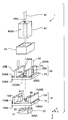
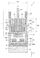
- FIG. 3 is a cross-sectional view of the optical module according to the first embodiment taken along line III-III in FIG. 2. It is a perspective view of the optical module of the modification 1 of 1st Embodiment. It is an upper surface penetration figure of the optical module of the modification 1 of 1st Embodiment. It is an upper surface penetration figure of the optical module of the modification 2 of 1st Embodiment. It is sectional drawing of the optical module of the modification 3 of 1st Embodiment. It is an exploded view of the imaging module of 2nd Embodiment.
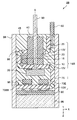
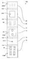
- FIG. 10 is a cross-sectional view taken along line XX of FIG. 9 of the imaging module according to the second embodiment. It is a perspective view of the imaging module of the modification 1 of 2nd Embodiment. It is sectional drawing of the imaging module of the modification 2 of 2nd Embodiment. It is an expanded view of the board
- the optical module 1 of this embodiment will be described with reference to FIGS. 1 to 3.
- the optical module 1 is an E / O module that converts an electrical signal into an optical signal and transmits the optical signal.
- the optical module 1 includes an optical element 30, a first substrate 10, relay substrates 15A and 15B, a holding substrate 20, side substrates 25A and 25B, a ferrule 40 as a holding member, an optical fiber 50, a signal Cable 60.
- the first substrate 10 and the relay substrates 15A and 15B are an integral three-dimensional substrate 19
- the holding substrate 20 and the side substrates 25A and 25B are an integral three-dimensional substrate 29.
- each of the side substrates 25A and 25B is referred to as a side substrate 25.
- the signal cable 60 transmits an electrical signal to the optical element 30, for example.
- the conducting wire at the tip is joined to the electrodes 21 of the side substrates 25A and 25B via solder (not shown). That is, the tip portions of the electrode 21 and the signal cable 60 are disposed in parallel with the optical axis O (Z axis).
- the ferrule 40 is a rectangular parallelepiped having a rectangular cross section in the direction perpendicular to the optical axis, and has four side surfaces 40SS.
- the ferrule 40 has a through hole H40 penetrating the upper surface and the lower surface. The tip of the optical fiber 50 is inserted into the through hole H40 and fixed with an adhesive.
- the first substrate 10 has a first main surface 10SA and a second main surface 10SB facing the first main surface 10SA.
- the optical element 30 is mounted on the first main surface 10SA. That is, the external terminal 32 of the optical element 30 is bonded to the bonding electrode of the first main surface 10SA, although not shown.
- a ferrule 40 is bonded to the second main surface 10SB.
- the front surface 30SA of the optical element 30 is parallel to the first main surface 10SA (XY plane) of the first substrate 10. That is, the optical axis O is parallel to the Z axis perpendicular to the first main surface 10SA. Since the first substrate 10 does not have a high light transmittance, a through hole H10 serving as an optical path is formed.
- the holding substrate 20 has a third main surface 20SA and a fourth main surface 20SB facing the third main surface 20SA.
- the third main surface 20SA and the fourth main surface 20SB are arranged in parallel to the second main surface 10SB and the first main surface 10SA of the first substrate 10.
- the holding substrate 20 has a rectangular opening (second through hole) H20 in plan view.
- the dimension of the opening H20 in the direction perpendicular to the optical axis, that is, the size in plan view, is the same as or slightly larger than the size in plan view of the ferrule 40.
- the four outer peripheral surfaces (side surfaces) 40SS of the quadrangular columnar ferrule 40 inserted into the opening H20 are in contact with the four wall surfaces H20SS of the opening H20 that is rectangular in plan view.
- the relay boards 15A and 15B arranged opposite to each other have substantially the same configuration.
- the relay substrate 15 connects the first substrate 10 and the holding substrate 20. That is, the main surface of the relay substrate 15 is disposed parallel to the optical axis O (Z axis), the lower end surface 15SSA is disposed on the outer peripheral portion of the second main surface 10SB of the first substrate 10, and the upper end surface 15SSB is
- the holding substrate 20 is connected to the outer peripheral portion of the third main surface 20SA.
- the side substrates 25A and 25B arranged opposite to each other have substantially the same configuration.
- the end surface of the side substrate 25 is disposed on the outer peripheral portion of the fourth main surface 20SB of the holding substrate 20. That is, in the side substrate 25, the fifth main surface (inner surface) 25SA and the sixth main surface (outer surface) 25SB are arranged in parallel to the optical axis O (Z axis).
- the optical fiber 50 is inserted into the through hole H40 and fitted, whereby the light emitting portion 31 of the optical element 30 and the optical fiber 50 are positioned. That is, the ferrule 40 is disposed on the second main surface 10SB of the first substrate 10 in a state where the central axis of the through hole H40 is disposed so as to coincide with the optical axis of the optical element 30.
- the inner shape of the through-hole H40 may be a prismatic shape such as a quadrangular prism or a hexagonal prism as long as the optical fiber 50 can be held by the wall surface in addition to the cylinder.
- the space surrounded by the side substrates 25A and 25B and in which the ferrule 40 is disposed is filled with a resin member 45.
- the resin member 45 is made of, for example, an epoxy resin.
- the resin member 45 is not an essential component of the optical module, but the optical module 1 in which the ferrule 40 is firmly fixed by the resin member 45 has higher reliability.
- the ferrule 40 is positioned in the in-plane direction (XY direction) of the ferrule 40 by the four outer peripheral surfaces (side surfaces) 40 SS being in contact with the four wall surfaces H 20 SS of the opening H 20 of the holding substrate 20. At the same time, the ferrule 40 is stably held.
- the optical module 1 has high transmission efficiency and reliability.
- the first substrate 10 and the relay substrates 15A and 15B are an integral three-dimensional substrate 19 made of ceramic, and have wiring (not shown).
- the holding substrate 20 and the side substrates 25A and 25B are an integral three-dimensional substrate 29 made of ceramic.
- the three-dimensional substrates 19 and 29 may be formed of a molded circuit component (MID: Molded Interconnect Device) having a non-conductive resin as a base material and having wiring (not shown), electrodes, and the like.
- MID Molded Interconnect Device
- the optical module 1 Since the first substrate 10 and the relay substrate 15 are accurately and firmly connected to the three-dimensional substrates 19 and 29, the optical module 1 is easy to manufacture.
- the optical module 1 has a small size and a small diameter in the direction perpendicular to the optical axis.
- the electrode 21 of the side substrates 25A and 25B that is, the joint portion of the signal cable 60 is included in the second space S40 obtained by extending the ferrule 40 in the direction orthogonal to the optical axis O. For this reason, the optical module 1 is short and small.
- an electronic component 96 that is a chip-shaped surface mounting component (SMD) such as a capacitor, an inductor, or a signal processing IC is mounted on the inner surface of the relay substrate 15. That is, since the first substrate 10 is large in the optical module 1, there is a gap between the relay substrate 15 and the ferrule 40. The electronic component 96 is disposed in the gap.
- SMD chip-shaped surface mounting component
- the optical module 1 since the electronic component 96 is mounted in a location close to the optical element 30, the wiring between the optical element 30 and the electronic component 96 is short. For this reason, the optical module 1 is not easily affected by noise, for example.
- the material of the ferrule 40 is a metal member such as SUS, ceramic, silicon, or glass. As will be described later, the ferrule 40 may be a substantially cylindrical, conical, or polygonal column.
- the plan view shape of the opening of the holding substrate is designed according to the shape of the ferrule. For example, when the ferrule is a regular hexagonal column, the opening of the holding substrate is a regular hexagon in plan view.
- the side substrates 25A and 25B are arranged to face each other so as to surround the ferrule 40 that is a holding member.
- the distance from the optical axis O to the side substrates 25A and 25B may not be the same.
- the side substrate 25A and the side substrate 25B may have different shapes (width / thickness).
- the number of the side substrates 25 may be 1 or more and 4 or less, but 2 or more is particularly preferable. Further, as long as the plurality of side surface substrates 25 are arranged so as to surround the ferrule 40, they may be arranged at positions orthogonal to each other or opposed to each other. For example, when the three side substrates 25 are included, the two side substrates are arranged at positions facing each other, one at a position orthogonal to the other two.
- the electrode 21 is disposed on at least one of the fifth main surface 25SA and the sixth main surface 25SB. In the case of including a plurality of side substrates, it is sufficient that the electrode 21 is disposed on at least one of the side substrates 25.
- the number of relay substrates 15 may be 1 or more and 4 or less, but 2 or more is particularly preferable in order to stably hold the first substrate 10 and the holding substrate 20. Moreover, it is preferable that each main surface is arrange
- the optical element is a light emitting element having a light emitting portion.
- an optical module in which the optical element is a light receiving element having a light receiving portion such as a photodiode has the same effect as the optical module 1.
- the opening of the holding substrate 20A is a notch T20 having a rectangular shape in plan view.
- the three inner peripheral surfaces of the opening with which the three outer peripheral surfaces (side surfaces) 40SS of the ferrule 40 are in contact are the three wall surfaces T20SS of the notch T20 of the holding substrate 20A.
- the opening of the holding substrate 20A may be the second through hole H20 or the cutout T20 as long as the ferrule 40 has a positioning function and a holding function.
- the first substrate 10A, the relay substrate 15, the holding substrate 20A, and the side substrates 25A and 25B are an FPC substrate, a ceramic substrate, a glass epoxy substrate, a glass substrate, a silicon substrate, and the like.
- the end surface of the relay substrate 15 is fixed to the second main surface 10SB of the first substrate 10A with an adhesive, and the wiring of the first substrate 10A and the wiring of the relay substrate 15A are, for example, via a conductive paste. Is conducting.
- the optical module 1B of the present modification has three side substrates 25A, 25B, and 25C.
- the main surfaces of the side substrates 25A and 25B are arranged at opposing positions, that is, rotationally symmetric positions.
- the main surface of the side substrate 25C is disposed at a position orthogonal to the main surfaces of the side substrates 25A and 25B.
- the side substrates 25A, 25B, 25C and the holding substrate 20B are configured by an integral three-dimensional substrate 29B made of ceramic. For this reason, the side substrates 25A, 25B, and 25C are U-shaped integral structures, and their boundaries are not clear.
- the two side surfaces 40SS of the ferrule 40 are in contact with the two wall surfaces T20SS of the notch T20. If at least two side surfaces 40SS of the ferrule 40 are in contact with the two wall surfaces T20SS of the notch T20, the ferrule 40 can be easily positioned in the in-plane direction.
- the side substrate 25B has the electrode 21 to which the signal cable 60 is joined also on the fifth main surface (inner surface) 25SA.
- the electrode 21 may be disposed only on the fifth main surface (inner surface) 25SA of the side substrate 25. That is, the electrode 21 may be disposed on at least one of the fifth main surface (inner surface) 25SA and the fourth main surface (outer surface) 25B of the side substrate 25.
- the three-dimensional board 19 ⁇ / b> C and the like are disposed inside a casing 99 that is a cylindrical member.
- the internal space of the housing 99 is filled with a resin 45.
- the optical element 30, the signal cable 60, and the ferrule 40 can be disposed on the flat substrate 19C.
- the substrate 19 ⁇ / b> C is three-dimensionalized by bending the connecting portion after the constituent members are disposed, and is disposed inside the housing 99. For this reason, the optical module 1C is easy to manufacture.
- the housing 99 may be a common member with other members instead of the dedicated member of the optical module 1C.
- the substrate 19C or the like may be inserted into a through hole formed in the distal end rigid portion of the endoscope and fixed by the resin 45.
- the imaging module 2 of the present embodiment includes the optical module 1, the imaging device 90, the second substrate 70, and the second relay substrates 75A and 75B of the first embodiment. Are provided.
- the signal cable 60 transmits an electrical signal to the image sensor 90 and the like.
- An imaging signal output from the imaging element 90 is converted into an optical signal by the optical element 30 and transmitted via the optical fiber 50.
- the imaging element 90 has a light receiving surface 90SA and a back surface 90SB facing the light receiving surface 90SA, and outputs an imaging signal.
- a light receiving portion 91 such as a CCD or CMOS light receiving circuit is formed on the light receiving surface 90SA of the image sensor 90.
- the light receiving portion 91 is a back surface through a through wiring (not shown) such as TSV (Through-Silicon Via). It is connected to a 90SB junction terminal 92.
- a cover glass 95 that protects the light receiving portion 91 is bonded to the light receiving surface 90SA. Note that the cover glass 95 is not an essential component of the imaging module 2.
- the second substrate 70 has a seventh main surface 70SA and an eighth main surface 70SB facing the seventh main surface 70SA, and the image sensor 90 is bonded to the seventh main surface 70SA.
- the second relay boards 75A and 75B connect the first board 10 and the second board 70. That is, in this embodiment, the second relay boards 75A and 75B having the same configuration are provided.
- the second relay board 75 has one end surface arranged perpendicular to the first main surface 10SA of the first substrate 10 and the other end surface arranged vertically to the eighth main surface 70SB of the second substrate 70. Has been.
- the second substrate 70 and the second relay substrates 75A and 75B are an integrated three-dimensional substrate 79 made of ceramic.
- the three-dimensional board 79 may be a molded circuit component.
- the second substrate 70, the second relay substrate 75, the first substrate 10, the relay substrate 15, and the holding substrate are in a space S ⁇ b> 10 in which the image sensor 90 is extended in the optical axis O direction.
- the side substrates 25 ⁇ / b> A and 25 ⁇ / b> B, the optical element 30, the ferrule 40, and the signal cable 60 are in a small diameter.
- the image sensor 90 having a large number of pixels has a large size in plan view. Therefore, the side substrates 25A and 25B and the signal cable 60 can be easily arranged around the ferrule 40.
- the electrode 21 of the side substrates 25A and 25B that is, the joint portion of the signal cable 60 is included in the second space S40 obtained by extending the ferrule 40 in the direction orthogonal to the optical axis O. For this reason, the imaging module 2 is short and small.
- the imaging module 2 is thin, short, and has high transmission efficiency and reliability.
- the optical element 30 is accommodated in a space formed by the second relay boards 75A and 75B.
- a chip-shaped electronic component 96 such as a capacitor, an inductor, or a signal processing IC is mounted on the eighth main surface 70SB of the second substrate 70 facing the back surface 90SB of the image sensor 90. And is accommodated in the same space as the optical element 30.
- the distance between the image sensor 90 and the electronic component 96 is close to the thickness of the second substrate 70 only slightly. If, for example, a decoupling capacitor is arranged at a position close to the image sensor 90, the influence of noise can be efficiently reduced.
- the electronic component 96 is in the space S10 obtained by extending the image sensor 90 in the optical axis O direction, the first substrate 10, the second substrate 70, the side substrates 25A and 25B, and the second relay substrate 75A, It may be mounted on any main surface of 75B.
- the imaging module 2A of the first modification of the second embodiment includes an optical module 1A, an imaging device 90, a second substrate 70A, three second relay substrates 75A to 75C, Have
- the second relay boards 75A and 75B are arranged at positions facing each other, and the second relay boards 75A and 75C are arranged at positions orthogonal to each other.
- the second relay substrate 75 connecting the first substrate 10A and the second substrate 70A has a main surface arranged in parallel to the optical axis O, and the main surface is the first main surface 10SA and the eighth substrate. Arranged perpendicularly to main surface 70SB.
- the number of the second relay boards 75 may be 1 to 4 as in the case of the side board of the optical module 1 already described.
- the imaging module 2B of the second modification of the second embodiment is similar to the optical module 1C.
- the second substrate 70, the second relay substrate 75, the first substrate 10, the relay substrate 15, the holding substrate 20, and the side substrate 25 are connected to each other via a flexible connection portion 10V.
- the integrated substrate 19B having the advantages of a rigid substrate and a flexible substrate, that is, a so-called rigid flexible substrate.
- the imaging element 90 and the like are housed in a hollow portion of the housing 99 and sealed with a resin 45.
- An electronic component 96 is mounted on the eighth main surface 70SB of the second substrate 70E.
- the connecting portion 10V of the substrate 19B is a flexible substrate having, for example, polyimide as a base.
- the second substrate 70, the second relay substrate 75, the first substrate 10, the relay substrate 15, the holding substrate 20, and the side substrate 25 are rigid substrates.
- the first substrate 10 has a through hole H10 serving as an optical path.
- the flat substrate 19B shown in FIG. 13 becomes a three-dimensional substrate by bending the connecting portion. Since the image pickup device, the optical device, the signal cable, the ferrule, and the like can be arranged on the flat substrate 19B before the bending process, the image pickup module 2B is easy to manufacture.
- the solid substrate 19B may be flexible as a whole or a multilayer substrate.
- the three-dimensional board 19B may have 1 to 4 side boards, 1 to 4 relay boards, and 1 to 4 second relay boards.
- the imaging module 2C is even shorter than the imaging module 2 or the like.
- the side substrate 25 ⁇ / b> D has a function of a holding substrate. That is, positioning and holding are performed by the outer peripheral surface 40SS of the ferrule 40 coming into contact with the fifth main surface 25SA that is the inner surface of the side substrates 25DA and 25DB arranged to face each other.
- the fifth main surface 25SA of the side substrate 25D has the function of the wall surface of the opening of the holding substrate.
- the first substrate 10 and the side substrate 25D are an integral three-dimensional wiring board 19D.
- the side substrate 25D has the function of a relay substrate, the electrode 21 is disposed on the sixth main surface 25SB, and is further disposed at a rotationally symmetric position.
- the plurality of side substrates 25D have a function of a holding substrate, and the fifth main surface 25SA of the plurality of side substrates 25D is in contact with the outer peripheral surface of the holding member.
- the endoscope 9 of the third embodiment includes the imaging module 2 (or 2A to 2D) already described.
- the endoscope 9 includes an insertion portion 9B in which an imaging module 2 having a small diameter and a short size is accommodated in the distal end portion 9A, and an operation portion 9C disposed on the proximal end side of the insertion portion 9B.
- a universal cord 9D extending from the operation unit 9C. The universal cord 9D is connected to the signal cable 60 of the imaging module.
- the endoscope 9 Since the endoscope 9 has the imaging module 2 having a small diameter and a short size and high transmission efficiency and reliability at the distal end portion 9A of the insertion portion 9B, the endoscope 9 is less invasive and highly reliable.
- the endoscope 9 is a flexible endoscope, but may be a rigid endoscope.
- the endoscope of the embodiment may be a medical endoscope or an industrial endoscope.
Landscapes
- Physics & Mathematics (AREA)
- Health & Medical Sciences (AREA)
- Life Sciences & Earth Sciences (AREA)
- Optics & Photonics (AREA)
- Surgery (AREA)
- Engineering & Computer Science (AREA)
- General Physics & Mathematics (AREA)
- Biomedical Technology (AREA)
- Molecular Biology (AREA)
- Nuclear Medicine, Radiotherapy & Molecular Imaging (AREA)
- Pathology (AREA)
- Radiology & Medical Imaging (AREA)
- Multimedia (AREA)
- Signal Processing (AREA)
- Heart & Thoracic Surgery (AREA)
- Medical Informatics (AREA)
- Biophysics (AREA)
- Animal Behavior & Ethology (AREA)
- General Health & Medical Sciences (AREA)
- Public Health (AREA)
- Veterinary Medicine (AREA)
- Endoscopes (AREA)
- Electromagnetism (AREA)
- Optical Couplings Of Light Guides (AREA)
Abstract
Un module optique 1 est pourvu : d'un élément optique 30; d'un premier substrat 10, sur lequel est monté l'élément optique 30, ledit élément optique étant sur une première surface principale 10 SA; un élément de maintien 40 qui est disposé sur une deuxième surface principale 10 SB du premier substrat 10; une fibre optique 50 insérée dans un trou traversant H40 de l'élément de maintien 40; un substrat de maintien 20, une surface principale 20 SA est disposée parallèlement à la surface principale 10 SA du premier substrat 10, ledit substrat de maintien ayant une ouverture H20 qui a une surface de paroi H20SS en contact avec une surface périphérique externe 40 SS de l'élément de maintien 40; un substrat de relais reliant le premier substrat et le substrat de maintien l'un à l'autre; un substrat de surface latérale, dans laquelle une surface principale 25 SB est disposée parallèlement à un axe optique O, une partie d'extrémité est reliée au substrat de maintien 20, et une électrode 21 est disposée sur la surface principale 25 SB; et un câble de signal 60, dont une partie d'extrémité avant est connectée à l'électrode 21 du substrat de surface latérale 25.
Priority Applications (3)
| Application Number | Priority Date | Filing Date | Title |
|---|---|---|---|
| PCT/JP2016/084071 WO2018092234A1 (fr) | 2016-11-17 | 2016-11-17 | Module optique,capture d'image et endoscope |
| JP2018550933A JPWO2018092234A1 (ja) | 2016-11-17 | 2016-11-17 | 光モジュール、撮像モジュールおよび内視鏡 |
| US16/406,433 US10750941B2 (en) | 2016-11-17 | 2019-05-08 | Optical module, image pickup module, and endoscope |
Applications Claiming Priority (1)
| Application Number | Priority Date | Filing Date | Title |
|---|---|---|---|
| PCT/JP2016/084071 WO2018092234A1 (fr) | 2016-11-17 | 2016-11-17 | Module optique,capture d'image et endoscope |
Related Child Applications (1)
| Application Number | Title | Priority Date | Filing Date |
|---|---|---|---|
| US16/406,433 Continuation US10750941B2 (en) | 2016-11-17 | 2019-05-08 | Optical module, image pickup module, and endoscope |
Publications (1)
| Publication Number | Publication Date |
|---|---|
| WO2018092234A1 true WO2018092234A1 (fr) | 2018-05-24 |
Family
ID=62146351
Family Applications (1)
| Application Number | Title | Priority Date | Filing Date |
|---|---|---|---|
| PCT/JP2016/084071 Ceased WO2018092234A1 (fr) | 2016-11-17 | 2016-11-17 | Module optique,capture d'image et endoscope |
Country Status (3)
| Country | Link |
|---|---|
| US (1) | US10750941B2 (fr) |
| JP (1) | JPWO2018092234A1 (fr) |
| WO (1) | WO2018092234A1 (fr) |
Cited By (4)
| Publication number | Priority date | Publication date | Assignee | Title |
|---|---|---|---|---|
| WO2021040047A1 (fr) * | 2019-08-29 | 2021-03-04 | 株式会社フジクラ | Émetteur, récepteur et système de communication |
| WO2021040049A1 (fr) * | 2019-08-29 | 2021-03-04 | 株式会社フジクラ | Émetteur, récepteur et système de communication |
| WO2021250727A1 (fr) * | 2020-06-08 | 2021-12-16 | オリンパス株式会社 | Module électronique, procédé de fabrication de module électronique et endoscope |
| JP2022127138A (ja) * | 2021-02-19 | 2022-08-31 | 矢崎総業株式会社 | 光結合構造、光結合法方法、カメラモジュール |
Families Citing this family (2)
| Publication number | Priority date | Publication date | Assignee | Title |
|---|---|---|---|---|
| JP7687926B2 (ja) * | 2021-10-01 | 2025-06-03 | Hoya株式会社 | 光送信モジュールおよび内視鏡 |
| JP2023053513A (ja) * | 2021-10-01 | 2023-04-13 | Hoya株式会社 | 光送信モジュールおよび内視鏡 |
Citations (5)
| Publication number | Priority date | Publication date | Assignee | Title |
|---|---|---|---|---|
| JPH04218136A (ja) * | 1990-08-27 | 1992-08-07 | Olympus Optical Co Ltd | 固体撮像装置 |
| JPH0549602A (ja) * | 1991-08-27 | 1993-03-02 | Olympus Optical Co Ltd | 内視鏡 |
| JP2008118568A (ja) * | 2006-11-07 | 2008-05-22 | Olympus Medical Systems Corp | 撮像装置 |
| JP2014137584A (ja) * | 2013-01-18 | 2014-07-28 | Olympus Corp | 光伝送モジュールおよび撮像装置 |
| JP2015068835A (ja) * | 2013-09-26 | 2015-04-13 | オリンパス株式会社 | 光伝送モジュール、及び内視鏡 |
Family Cites Families (3)
| Publication number | Priority date | Publication date | Assignee | Title |
|---|---|---|---|---|
| US7736382B2 (en) * | 2005-09-09 | 2010-06-15 | Lockheed Martin Corporation | Apparatus for optical stimulation of nerves and other animal tissue |
| US9706903B2 (en) * | 2009-06-18 | 2017-07-18 | Endochoice, Inc. | Multiple viewing elements endoscope system with modular imaging units |
| JP6411088B2 (ja) * | 2013-09-26 | 2018-10-24 | オリンパス株式会社 | 光伝送モジュールおよび内視鏡 |
-
2016
- 2016-11-17 JP JP2018550933A patent/JPWO2018092234A1/ja active Pending
- 2016-11-17 WO PCT/JP2016/084071 patent/WO2018092234A1/fr not_active Ceased
-
2019
- 2019-05-08 US US16/406,433 patent/US10750941B2/en active Active
Patent Citations (5)
| Publication number | Priority date | Publication date | Assignee | Title |
|---|---|---|---|---|
| JPH04218136A (ja) * | 1990-08-27 | 1992-08-07 | Olympus Optical Co Ltd | 固体撮像装置 |
| JPH0549602A (ja) * | 1991-08-27 | 1993-03-02 | Olympus Optical Co Ltd | 内視鏡 |
| JP2008118568A (ja) * | 2006-11-07 | 2008-05-22 | Olympus Medical Systems Corp | 撮像装置 |
| JP2014137584A (ja) * | 2013-01-18 | 2014-07-28 | Olympus Corp | 光伝送モジュールおよび撮像装置 |
| JP2015068835A (ja) * | 2013-09-26 | 2015-04-13 | オリンパス株式会社 | 光伝送モジュール、及び内視鏡 |
Cited By (9)
| Publication number | Priority date | Publication date | Assignee | Title |
|---|---|---|---|---|
| WO2021040047A1 (fr) * | 2019-08-29 | 2021-03-04 | 株式会社フジクラ | Émetteur, récepteur et système de communication |
| JPWO2021040047A1 (fr) * | 2019-08-29 | 2021-03-04 | ||
| WO2021040049A1 (fr) * | 2019-08-29 | 2021-03-04 | 株式会社フジクラ | Émetteur, récepteur et système de communication |
| JPWO2021040049A1 (fr) * | 2019-08-29 | 2021-03-04 | ||
| CN114223153A (zh) * | 2019-08-29 | 2022-03-22 | 株式会社藤仓 | 发送器、接收器以及通信系统 |
| WO2021250727A1 (fr) * | 2020-06-08 | 2021-12-16 | オリンパス株式会社 | Module électronique, procédé de fabrication de module électronique et endoscope |
| US12501543B2 (en) | 2020-06-08 | 2025-12-16 | Olympus Corporation | Electronic module, manufacturing method for electronic module, and endoscope |
| JP2022127138A (ja) * | 2021-02-19 | 2022-08-31 | 矢崎総業株式会社 | 光結合構造、光結合法方法、カメラモジュール |
| JP7210120B2 (ja) | 2021-02-19 | 2023-01-23 | 矢崎総業株式会社 | 光結合構造、光結合法方法、カメラモジュール |
Also Published As
| Publication number | Publication date |
|---|---|
| JPWO2018092234A1 (ja) | 2019-10-10 |
| US10750941B2 (en) | 2020-08-25 |
| US20190261842A1 (en) | 2019-08-29 |
Similar Documents
| Publication | Publication Date | Title |
|---|---|---|
| US10786143B2 (en) | Optical module, image pickup module, and endoscope | |
| US10750941B2 (en) | Optical module, image pickup module, and endoscope | |
| JP6411088B2 (ja) | 光伝送モジュールおよび内視鏡 | |
| JP5926890B2 (ja) | 配線板、配線板の製造方法、および撮像装置 | |
| JP6321933B2 (ja) | 光伝送モジュール、及び内視鏡 | |
| WO2018173261A1 (fr) | Endoscope et module composite photoélectrique | |
| WO2018092318A1 (fr) | Module d'imagerie endoscopique et endoscope | |
| WO2014112461A1 (fr) | Module de transmission optique et dispositif d'imagerie | |
| US20180078114A1 (en) | Endoscope and optical transmission module | |
| WO2019207650A1 (fr) | Dispositif d'imagerie d'endoscope, endoscope et procédé de fabrication de dispositif d'imagerie d'endoscope | |
| WO2018198188A1 (fr) | Endoscope et module d'imagerie | |
| JP6659826B2 (ja) | 光伝送モジュール及び内視鏡 | |
| WO2017037828A1 (fr) | Endoscope, unité électronique, et procédé de fabrication d'une unité électronique | |
| WO2022244133A1 (fr) | Unité d'imagerie, procédé de production d'unité d'imagerie et endoscope | |
| US9874706B2 (en) | Optical transmission module and method for manufacturing optical transmission module | |
| WO2017085877A1 (fr) | Procédé de fabrication de dispositif à semi-conducteur, dispositif à semi-conducteur et endoscope | |
| JP2000083896A (ja) | 内視鏡用撮像装置 | |
| US10470642B2 (en) | Optical transmitter and endoscope | |
| JP6188479B2 (ja) | 基板モジュール | |
| JP2014108282A (ja) | 撮像装置、内視鏡及び撮像装置の製造方法 | |
| US20180368662A1 (en) | Optical transmission module and endoscope | |
| US20180220051A1 (en) | Endoscope, image pickup module, and manufacturing method of image pickup module | |
| WO2020089960A1 (fr) | Dispositif d'imagerie, endoscope, et procédé de production de dispositif d'imagerie | |
| WO2020179067A1 (fr) | Transducteur optique endoscopique, dispositif d'imagerie endoscopique et endoscope | |
| JP2018105907A (ja) | 光モジュールおよび内視鏡 |
Legal Events
| Date | Code | Title | Description |
|---|---|---|---|
| 121 | Ep: the epo has been informed by wipo that ep was designated in this application |
Ref document number: 16921933 Country of ref document: EP Kind code of ref document: A1 |
|
| ENP | Entry into the national phase |
Ref document number: 2018550933 Country of ref document: JP Kind code of ref document: A |
|
| NENP | Non-entry into the national phase |
Ref country code: DE |
|
| 122 | Ep: pct application non-entry in european phase |
Ref document number: 16921933 Country of ref document: EP Kind code of ref document: A1 |