WO2018097112A1 - Substrat multicouche, structure de montage de substrat multicouche sur carte de circuit imprimé, procédé de montage de substrat multicouche, et procédé de production de substrat multicouche - Google Patents
Substrat multicouche, structure de montage de substrat multicouche sur carte de circuit imprimé, procédé de montage de substrat multicouche, et procédé de production de substrat multicouche Download PDFInfo
- Publication number
- WO2018097112A1 WO2018097112A1 PCT/JP2017/041737 JP2017041737W WO2018097112A1 WO 2018097112 A1 WO2018097112 A1 WO 2018097112A1 JP 2017041737 W JP2017041737 W JP 2017041737W WO 2018097112 A1 WO2018097112 A1 WO 2018097112A1
- Authority
- WO
- WIPO (PCT)
- Prior art keywords
- conductor pattern
- plating film
- pattern
- conductor
- multilayer substrate
- Prior art date
- Legal status (The legal status is an assumption and is not a legal conclusion. Google has not performed a legal analysis and makes no representation as to the accuracy of the status listed.)
- Ceased
Links
Images






Classifications
-
- H—ELECTRICITY
- H01—ELECTRIC ELEMENTS
- H01F—MAGNETS; INDUCTANCES; TRANSFORMERS; SELECTION OF MATERIALS FOR THEIR MAGNETIC PROPERTIES
- H01F17/00—Fixed inductances of the signal type
- H01F17/0006—Printed inductances
- H01F17/0013—Printed inductances with stacked layers
-
- H—ELECTRICITY
- H05—ELECTRIC TECHNIQUES NOT OTHERWISE PROVIDED FOR
- H05K—PRINTED CIRCUITS; CASINGS OR CONSTRUCTIONAL DETAILS OF ELECTRIC APPARATUS; MANUFACTURE OF ASSEMBLAGES OF ELECTRICAL COMPONENTS
- H05K3/00—Apparatus or processes for manufacturing printed circuits
- H05K3/46—Manufacturing multilayer circuits
- H05K3/4611—Manufacturing multilayer circuits by laminating two or more circuit boards
- H05K3/4626—Manufacturing multilayer circuits by laminating two or more circuit boards characterised by the insulating layers or materials
- H05K3/4632—Manufacturing multilayer circuits by laminating two or more circuit boards characterised by the insulating layers or materials laminating thermoplastic or uncured resin sheets comprising printed circuits without added adhesive materials between the sheets
-
- H—ELECTRICITY
- H01—ELECTRIC ELEMENTS
- H01F—MAGNETS; INDUCTANCES; TRANSFORMERS; SELECTION OF MATERIALS FOR THEIR MAGNETIC PROPERTIES
- H01F27/00—Details of transformers or inductances, in general
- H01F27/28—Coils; Windings; Conductive connections
- H01F27/29—Terminals; Tapping arrangements for signal inductances
- H01F27/292—Surface mounted devices
-
- H—ELECTRICITY
- H01—ELECTRIC ELEMENTS
- H01F—MAGNETS; INDUCTANCES; TRANSFORMERS; SELECTION OF MATERIALS FOR THEIR MAGNETIC PROPERTIES
- H01F41/00—Apparatus or processes specially adapted for manufacturing or assembling magnets, inductances or transformers; Apparatus or processes specially adapted for manufacturing materials characterised by their magnetic properties
- H01F41/02—Apparatus or processes specially adapted for manufacturing or assembling magnets, inductances or transformers; Apparatus or processes specially adapted for manufacturing materials characterised by their magnetic properties for manufacturing cores, coils, or magnets
- H01F41/04—Apparatus or processes specially adapted for manufacturing or assembling magnets, inductances or transformers; Apparatus or processes specially adapted for manufacturing materials characterised by their magnetic properties for manufacturing cores, coils, or magnets for manufacturing coils
- H01F41/041—Printed circuit coils
- H01F41/042—Printed circuit coils by thin film techniques
-
- H—ELECTRICITY
- H01—ELECTRIC ELEMENTS
- H01F—MAGNETS; INDUCTANCES; TRANSFORMERS; SELECTION OF MATERIALS FOR THEIR MAGNETIC PROPERTIES
- H01F41/00—Apparatus or processes specially adapted for manufacturing or assembling magnets, inductances or transformers; Apparatus or processes specially adapted for manufacturing materials characterised by their magnetic properties
- H01F41/02—Apparatus or processes specially adapted for manufacturing or assembling magnets, inductances or transformers; Apparatus or processes specially adapted for manufacturing materials characterised by their magnetic properties for manufacturing cores, coils, or magnets
- H01F41/04—Apparatus or processes specially adapted for manufacturing or assembling magnets, inductances or transformers; Apparatus or processes specially adapted for manufacturing materials characterised by their magnetic properties for manufacturing cores, coils, or magnets for manufacturing coils
- H01F41/041—Printed circuit coils
- H01F41/043—Printed circuit coils by thick film techniques
-
- H—ELECTRICITY
- H05—ELECTRIC TECHNIQUES NOT OTHERWISE PROVIDED FOR
- H05K—PRINTED CIRCUITS; CASINGS OR CONSTRUCTIONAL DETAILS OF ELECTRIC APPARATUS; MANUFACTURE OF ASSEMBLAGES OF ELECTRICAL COMPONENTS
- H05K1/00—Printed circuits
- H05K1/02—Details
- H05K1/0296—Conductive pattern lay-out details not covered by sub groups H05K1/02 - H05K1/0295
- H05K1/0298—Multilayer circuits
-
- H—ELECTRICITY
- H05—ELECTRIC TECHNIQUES NOT OTHERWISE PROVIDED FOR
- H05K—PRINTED CIRCUITS; CASINGS OR CONSTRUCTIONAL DETAILS OF ELECTRIC APPARATUS; MANUFACTURE OF ASSEMBLAGES OF ELECTRICAL COMPONENTS
- H05K1/00—Printed circuits
- H05K1/16—Printed circuits incorporating printed electric components, e.g. printed resistors, capacitors or inductors
- H05K1/165—Printed circuits incorporating printed electric components, e.g. printed resistors, capacitors or inductors incorporating printed inductors
-
- H—ELECTRICITY
- H05—ELECTRIC TECHNIQUES NOT OTHERWISE PROVIDED FOR
- H05K—PRINTED CIRCUITS; CASINGS OR CONSTRUCTIONAL DETAILS OF ELECTRIC APPARATUS; MANUFACTURE OF ASSEMBLAGES OF ELECTRICAL COMPONENTS
- H05K3/00—Apparatus or processes for manufacturing printed circuits
- H05K3/46—Manufacturing multilayer circuits
- H05K3/4611—Manufacturing multilayer circuits by laminating two or more circuit boards
- H05K3/4614—Manufacturing multilayer circuits by laminating two or more circuit boards the electrical connections between the circuit boards being made during lamination
-
- H—ELECTRICITY
- H05—ELECTRIC TECHNIQUES NOT OTHERWISE PROVIDED FOR
- H05K—PRINTED CIRCUITS; CASINGS OR CONSTRUCTIONAL DETAILS OF ELECTRIC APPARATUS; MANUFACTURE OF ASSEMBLAGES OF ELECTRICAL COMPONENTS
- H05K3/00—Apparatus or processes for manufacturing printed circuits
- H05K3/46—Manufacturing multilayer circuits
- H05K3/4611—Manufacturing multilayer circuits by laminating two or more circuit boards
- H05K3/4614—Manufacturing multilayer circuits by laminating two or more circuit boards the electrical connections between the circuit boards being made during lamination
- H05K3/462—Manufacturing multilayer circuits by laminating two or more circuit boards the electrical connections between the circuit boards being made during lamination characterized by laminating only or mainly similar double-sided circuit boards
-
- H—ELECTRICITY
- H05—ELECTRIC TECHNIQUES NOT OTHERWISE PROVIDED FOR
- H05K—PRINTED CIRCUITS; CASINGS OR CONSTRUCTIONAL DETAILS OF ELECTRIC APPARATUS; MANUFACTURE OF ASSEMBLAGES OF ELECTRICAL COMPONENTS
- H05K3/00—Apparatus or processes for manufacturing printed circuits
- H05K3/46—Manufacturing multilayer circuits
- H05K3/4644—Manufacturing multilayer circuits by building the multilayer layer by layer, i.e. build-up multilayer circuits
- H05K3/4652—Adding a circuit layer by laminating a metal foil or a preformed metal foil pattern
-
- H—ELECTRICITY
- H05—ELECTRIC TECHNIQUES NOT OTHERWISE PROVIDED FOR
- H05K—PRINTED CIRCUITS; CASINGS OR CONSTRUCTIONAL DETAILS OF ELECTRIC APPARATUS; MANUFACTURE OF ASSEMBLAGES OF ELECTRICAL COMPONENTS
- H05K1/00—Printed circuits
- H05K1/18—Printed circuits structurally associated with non-printed electric components
- H05K1/181—Printed circuits structurally associated with non-printed electric components associated with surface mounted components
Definitions
- the present invention relates to a multilayer substrate in which base materials made of an insulating resin having conductor patterns formed on both sides are laminated and thermocompression bonded, a mounting structure on the circuit substrate, a mounting method thereof, and a manufacturing method thereof.
- a coil pattern with a narrow pitch may be formed by plating on a multilayer substrate formed by laminating a base material on which a conductor pattern is formed by hot pressing in order to increase the density.
- conductor patterns may be formed on both surfaces of the base material.
- Patent Document 1 describes a coil component in which a conductor pattern is formed on both surfaces of a base material made of an insulating resin, and a plating film is formed on the conductor pattern to form a laminated coil component.
- the thicker the plating film the larger the cross-sectional area of the conductor pattern, so the resistance value per unit length of the conductor pattern Becomes lower.
- the growth rate (deposition rate) of the plating film varies depending on the convection state of the plating solution in the plating bath, the distance between electrodes in the case of electroplating, the difference in the shape of the conductor pattern, and the like. Therefore, the thicker the plating film, the greater the difference in film thickness, and the thickness and width of the conductor pattern are likely to be uneven. For this reason, when the distance between the centers of adjacent conductor patterns is reduced (with a narrow pitch) and the conductor patterns are formed at a high density, the conductor patterns come into contact with each other, and a short circuit is likely to occur.
- An object of the present invention is to provide a multilayer board in which short circuit in the laminating direction between conductive patterns formed with plating films is suppressed, a mounting structure of the multilayer board on a circuit board, a mounting method of the multilayer board, and the multilayer It is to provide a method for manufacturing a substrate.
- the multilayer substrate of the present invention is A plurality of resin base materials; A bonding layer sandwiched between resin substrates adjacent to each other in the stacking direction of the plurality of resin substrates; A plurality of conductor patterns formed on both surfaces of the plurality of resin bases, the surface being a plating film; and
- the plurality of resin base materials include a first resin base material having a first surface, a second surface opposite to the first surface, a third surface facing the second surface, and the third surface.
- a second resin base material having a fourth surface that is opposite to the surface The plurality of conductor patterns are formed on the first surface and have a first conductor pattern whose surface is a plating film, a second conductor pattern which is formed on the second surface and whose surface is a plating film, and the third A third conductor pattern formed on the surface and having a surface that is a plating film; and a fourth conductor pattern formed on the fourth surface and having a surface that is a plating film;
- the first conductor pattern does not face the other conductor pattern, and is positioned closer to one outermost layer than the second conductor pattern,
- the film thickness of the plating film of the second conductor pattern is thinner than the film thickness of the plating film of the first conductor pattern,
- a plurality of layers including the first resin base material, the bonding layer, and the second resin base material were laminated and thermocompression bonded, It is characterized by that.
- the thick first conductor pattern when the thick first conductor pattern is positioned near the outermost layer, heat is easily transmitted to the inside of the multilayer body through the first conductor pattern having high thermal conductivity. Therefore, the amount of heat of the heating press required for joining the inner layers can be reduced, and the amount of heat applied to the resin substrate closer to the outermost layer can be relatively reduced, so that deformation (thermal deformation) accompanied by resin flow can be suppressed.
- the conductor pattern on the second surface is relatively thin, the risk of short circuit between the conductor pattern on the second surface and the conductor pattern opposed via the bonding layer is reduced. Therefore, the risk of a short circuit is reduced as compared with a conductor pattern in which all of the plurality of conductor patterns have a plating film having the same thickness and the multilayer substrate has the same laminated thickness. For the same reason, the thickness of the multilayer substrate can be reduced. Further, a multilayer substrate having a low resistance conductor pattern can be obtained as compared with a structure in which all of the plurality of conductor patterns are conductor patterns having a thin plating film.
- the joining layer has higher fluidity at a predetermined pressing temperature than the plurality of resin base materials.
- the bonding layer easily flows at the press temperature, interlayer short circuit due to thermal deformation during pressing is suppressed.
- the film thickness of the plating film of the third conductor pattern is thinner than the film thickness of the plating film of the fourth conductor pattern.
- the thickness of the conductor pattern embedded in the resin base material (that is, the thickness of the resin base material) also acts as the thickness of the plating film. Therefore, if the distance between the conductor patterns adjacent in the stacking direction is the same, the cross-sectional area of the conductor pattern can be increased accordingly, and if the cross-sectional area of the conductor pattern is the same, the distance between the conductor patterns adjacent in the stacking direction is increased. Can be big.
- the base is a metal foil, and the thickness of the plating film is thicker than the thickness of the base It is preferable.
- the base electrode can form a conductive pattern with a narrow pitch (the distance between the centers of adjacent conductive patterns is narrow) by photolithography or the like, and the plating film becomes a conductive pattern with a high aspect ratio in the thickness direction due to its growth. . Therefore, although the chip is a narrow chip, the cross-sectional area of the conductor pattern is increased, and the resistance value per unit length can be effectively reduced. Further, as the thickness of the plating film increases, the difference in the thickness of the plating film becomes more prominent. However, according to the present invention, even when the plating film thickness is large, the above structure prevents short circuit. .
- the metal foil is a copper foil and the plating film is a copper plating film.
- the plating film is a copper plating film.
- the plurality of conductor patterns include a thick conductor pattern of a plating film formed according to a surface to be formed and a thin conductor pattern of a plating film, and among the plurality of conductor patterns, through the bonding layer. It is preferable that the conductor patterns facing each other partially overlap each other in plan view and form a pair of the thin conductor pattern and the thick conductor pattern or a pair of the thin conductor pattern and the thin conductor pattern. With this structure, the thick conductor pattern and the thick conductor pattern do not face each other in the stacking direction, and a short circuit between them is prevented.
- the difference in the film thickness of the plating film is small, so the margin between the layers can be reduced (can be made closer), and the thickness dimension of the laminate can be reduced accordingly. Can be small.
- the first conductor pattern and the third conductor pattern are thick conductor patterns of the plating film
- the second conductor pattern and the fourth conductor pattern are thin conductor patterns of the plating film
- the second resin base material is preferably closer to the mounting surface than the first resin base material.
- the second conductor patterns are arranged at a constant pitch in the cross section in the stacking direction, the third conductor patterns are arranged at a constant pitch in the cross section, and the arrangement of the first conductor pattern is the above It is preferable that the direction is shifted in the pitch direction.
- the second conductor pattern and the third conductor pattern are opposed to each other in the direction where the thickest portion is inclined from the stacking direction (oblique direction), so that the distance between the second surface and the third surface is greater. Even if it is narrow, a short circuit between the second conductor pattern and the third conductor pattern is prevented.
- the conductor pattern is preferably a coil conductor pattern. According to this structure, since the coil conductor pattern has a structure in which the conductor patterns are arranged at a narrow pitch, the thermal conductivity is high, and the effect of the present invention becomes remarkable.
- the terminal electrode is formed at a position that does not overlap the conductor pattern in plan view.
- the mounting structure of the multilayer substrate of the present invention on a circuit board is as follows: A multilayer board according to (11) or (12) above, and a circuit board on which the multilayer board is mounted, wherein the terminal electrode is connected to a pad electrode formed on the circuit board. .
- the thermal conductivity during heating of the laminate is high.
- the surface close to the first resin base of the multilayer board is heated with a hot bar or the like, but the heat is quickly conducted to the bonding material such as solder on the terminal electrode, A multilayer board can be mounted efficiently.
- the multilayer board mounting method of the present invention includes: A method of mounting the multilayer substrate according to (11) or (12) on a circuit board, wherein a surface opposite to the terminal electrode formation surface of the multilayer substrate is heated with a hot bar, and the terminal electrode is It connects to the pad electrode formed in the board
- the heat of the hot bar is quickly conducted to the bonding material such as solder on the terminal electrode, and the multilayer substrate can be mounted efficiently.
- a method for producing a multilayer substrate of the present invention includes: A base having substantially the same surface and the same thickness by patterning a copper foil on both surfaces of a first thermoplastic resin base material having a first surface and a second surface opposite to the first surface. Patterning of copper foil on both sides of a thermoplastic second resin substrate having a third surface facing the second surface and a fourth surface opposite the third surface, forming a pattern A base pattern forming step of forming a base pattern having substantially the same surface and the same thickness; A copper plating film is grown on the ground pattern on the first surface, a copper plating film is grown on the ground pattern on the second surface, and the copper plating film on the ground pattern on the second surface is greater than the copper plating film.
- the entire laminated body is heated more quickly at the time of hot pressing, and closer to the outermost surface.
- the phenomenon that only the first layer softens and flows first is suppressed. Therefore, an excessive approach of the interlayer distance due to the nonuniformity of the plating film is suppressed, and an interlayer short circuit is suppressed.
- the present invention it is possible to obtain a multilayer substrate in which short-circuiting in the laminating direction of conductor patterns formed with plating films is suppressed, and a mounting structure of the multilayer substrate on a circuit substrate.
- FIG. 1 is a perspective view of a multilayer substrate 101 of the present embodiment.
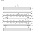
- FIG. 2A is a cross-sectional view of the multilayer substrate 101 before lamination of a plurality of resin base materials and bonding layers
- FIG. 2B is a cross-sectional view after the lamination.
- FIG. 2C is a cross-sectional view of the multilayer substrate 101 taken along the line AA in FIG.
- FIG. 3 is a cross-sectional view of the multilayer substrate 101 when stacked.
- FIG. 4 is an exploded perspective view of the multilayer substrate 101.
- FIG. 5 is a flowchart showing a manufacturing procedure of the multilayer substrate 101.
- FIG. 6 is a cross-sectional view of the multilayer substrate 102 according to the second embodiment.
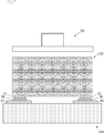
- FIG. 7 is a diagram showing a mounting structure of the multilayer substrate 102 on the circuit board and a mounting method of the multilayer substrate.
- FIG. 8 is a cross-sectional view of the multilayer substrate 103 according to the third embodiment.
- FIG. 9 is a diagram showing a mounting structure of a multilayer board 104 according to the fourth embodiment on a circuit board and a mounting method of the multilayer board.
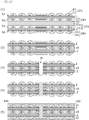
- FIG. 10 is a diagram illustrating a method of manufacturing the multilayer substrate 105 according to the fifth embodiment in the order of steps.
- FIG. 11 is a diagram illustrating the method of manufacturing the multilayer substrate 105 according to the fifth embodiment in the order of steps, and is a diagram following FIG. 10.
- FIG. 12 is a diagram illustrating a method of manufacturing the multilayer substrate 106 according to the sixth embodiment in the order of steps.
- FIG. 1 is a perspective view of a multilayer substrate 101 according to the first embodiment.
- the multilayer substrate 101 includes a laminate 100 including a plurality of resin base materials and a bonding layer sandwiched between resin base materials adjacent to each other in the stacking direction of the plurality of resin base materials.
- terminal electrodes 31 and 32 for surface mounting are formed on the lower surface of the multilayer substrate 101.
- FIG. 2A is a cross-sectional view of the multilayer substrate 101 before a plurality of resin base materials and bonding layers are laminated
- FIG. 2B is a cross-sectional view after the lamination
- FIG. 2C is a cross-sectional view of the multilayer substrate 101 taken along the line AA in FIG.
- FIG. 3 is a cross-sectional view of the multilayer substrate 101 when stacked. However, for convenience of illustration, the resin base material and the bonding layer are shown separately.
- FIG. 4 is an exploded perspective view of the multilayer substrate 101.
- the multilayer substrate 101 includes resin base materials 1 and 2, a bonding layer 10, and cover lays 21 and 22.
- the resin substrate 1 corresponds to the “first resin substrate” of the present invention
- the resin substrate 2 corresponds to the “second resin substrate” of the present invention.
- a first conductor pattern CP1 is formed on the first surface S1 of the first resin base material 1
- a second conductor pattern CP2 is formed on the second surface S2.
- a third conductor pattern CP3 is formed on the third surface S3 of the second resin base material 2
- a fourth conductor pattern CP4 is formed on the fourth surface S4.
- the first conductor pattern CP1 includes a base conductor pattern C1 and a plating film P1 formed on the surface thereof
- the second conductor pattern CP2 includes a base conductor pattern C2 and a plating film P2 formed on the surface thereof.
- the third conductor pattern CP3 is composed of a base conductor pattern C3 and a plating film P3 formed on the surface thereof
- the fourth conductor pattern CP4 is a base conductor pattern C4 and a plating film P4 formed on the surface thereof. It consists of and.
- These conductor patterns CP1, CP2, CP3, and CP4 form a single or a plurality of coil conductor patterns.
- the underlying conductor patterns C1, C2, C3, C4 are, for example, copper foil patterns, and the plating films P1, P2, P3, P4 are, for example, copper plating films.
- the thicknesses of the plating films P1, P2, P3, and P4 are thicker than those of the underlying conductor patterns C1, C2, C3, and C4.
- the first conductor pattern CP1 is positioned closer to one outermost layer (in this example, the cover lay 21) than the second conductor pattern CP2, and the second conductor pattern CP2 is thinner than the first conductor pattern CP1.
- the third conductor pattern CP3 is thinner than the fourth conductor pattern CP4.
- the second conductor pattern CP2 and the third conductor pattern CP3 overlap at least partially in plan view.
- An interlayer connection conductor V1 for connecting the first conductor pattern CP1 and the second conductor pattern CP2 is formed at a predetermined position of the first resin base material 1.
- an interlayer connection conductor V2 that connects the third conductor pattern CP3 and the fourth conductor pattern CP4 is formed at a predetermined position of the second resin base 2.
- An interlayer connection conductor V ⁇ b> 10 a is formed at a predetermined position of the bonding layer 10.
- the coverlays 21 and 22 and the bonding layer 10 are sheets of a thermosetting resin such as an epoxy resin, and the first resin substrate 1 and the second resin substrate 2 are sheets of a thermoplastic resin such as a liquid crystal polymer.
- the coverlays 21 and 22 and the bonding layer 10 have higher fluidity at a predetermined pressing temperature than the first resin base material 1 and the second resin base material 2.
- the bonding layer 10 is sandwiched between the resin base material 2, the cover lay 21 is disposed on the outer layer side of the first resin base material 1, and the cover lay 22 is disposed on the outer layer side of the second resin base material 2.
- each layer is sandwiched between press plates 51 and 52 and heated and pressed at a predetermined temperature and a predetermined pressure, thereby forming a laminate 100 as shown in FIG. .
- the cover lays 21 and 22 and the bonding layer 10 have higher fluidity at the press temperature than the first resin substrate 1 and the second resin substrate 2, the first resin substrate 1 and the second resin substrate 2 is filled with the bonding layer 10, the surface (upper surface) of the first resin base material 1 is filled with the cover lay 21, and the surface (lower surface) of the second resin base material 2 is filled with the cover lay 22.
- a resist film RF is formed on the surface of the laminate 100 as necessary.
- the second conductor pattern CP ⁇ b> 2 is illustrated separately from the lower surface of the first resin base material 1.
- the fourth conductor pattern CP4 is illustrated separately from the lower surface of the second resin base 2.
- Interlayer connection conductors V1a and V1b are formed on the first resin base material 1, and interlayer connection conductors V2a and V2b are formed on the second resin base material 2.
- Interlayer connection conductors V10a and V10b are formed on the bonding layer 10, and interlayer connection conductors V22a and V22b are formed on the cover lay 22.
- the first conductor pattern CP1, the second conductor pattern CP2, the third conductor pattern CP3, and the fourth conductor pattern CP4 are all rectangular spiral coil conductor patterns.
- the inner end of the first conductor pattern CP1 and the inner end of the second conductor pattern CP2 are connected via an interlayer connection conductor V1a.
- the outer end of the second conductor pattern CP2 and the outer end of the third conductor pattern CP3 are connected via an interlayer connection conductor V10a.
- the inner end of the third conductor pattern CP3 and the inner end of the fourth conductor pattern CP4 are connected via an interlayer connection conductor V2a.
- the outer terminal of the fourth conductor pattern CP4 and the terminal electrode 32 are connected via an interlayer connection conductor V22a.
- the outer terminal of the first conductor pattern CP1 and the terminal electrode 31 are connected via interlayer connection conductors V1b, V10b, V2b, V22b.
- the terminal electrodes 31 and 32 are formed at positions that do not overlap the coil conductor pattern in plan view.
- FIG. 5 is a flowchart showing a manufacturing procedure of the multilayer substrate 101 of the present embodiment.
- the multilayer substrate 101 is manufactured by processing in the order of a base pattern forming step S1, a plating step S2, and a laminated body forming step S3.
- a ground pattern is formed by photolithography on the first resin base material 1 covered with a double-sided copper foil. Moreover, a hole is formed in the formation position of the interlayer connection conductors V1 and V2 shown in FIG. Since the said copper foil becomes a base pattern, it exists in the same surface of a base pattern, and is the same thickness.
- plating step S2 A copper plating film is formed on the base pattern by electroplating.
- each conductor pattern is set to a predetermined plating thickness by controlling the time of the plating bath. For example, first, a resist film is formed on the second surface S2 of the first resin substrate 1, and in this state, the resist film is placed in a plating bath for a first predetermined time. As a result, a plating film having a predetermined thickness is formed on the first surface S1 of the first resin substrate 1. Subsequently, the resist film is removed and placed in a plating bath for a second fixed time.
- a plating film P2 having a thickness corresponding to the second constant time is formed on the second surface S2 of the first resin base material 1, and the first surface S1 of the first resin base material 1 is [first constant constant].
- a plating film P1 having a thickness corresponding to [time + second constant time] is formed.
- plating films P3 and P4 having different thicknesses are formed on the second resin base 2 as well.
- the interlayer connection conductors V1 and V2 are formed by forming a plating film in the holes where the interlayer connection conductors V1 and V2 are formed.
- a resin substrate is placed in a plating bath to form a plating film with a predetermined thickness on both sides, a resist film is formed on the surface on which the plating film is thinly formed, and a resist film is formed.
- a plating film on the surface that is not formed may be further grown.
- a resist film is formed on one surface, a plating film having a predetermined thickness is formed on the other surface, then the resist on one surface is removed, a resist film is formed on the other surface, and a predetermined thickness is formed on one surface.
- a plating film may be formed.
- the cover lay 22, the second resin base material 2, the bonding layer 10, the first resin base material 1, and the cover lay 21 are laminated in this order and heated and pressed at a predetermined temperature and a predetermined pressure. . For example, it presses at the temperature of 280 degreeC or more and 320 degrees C or less.
- a resist film RF is applied and formed on the surface of the laminate 100.
- the interlayer connection conductor V10a in the bonding layer 10 is formed before the multilayer body forming step S3. For example, a hole is formed in a predetermined position of the bonding layer 10, a protective sheet is pasted on one surface, a conductive paste is filled in the hole, and the protective sheet is peeled off to hold the conductive paste in the hole. The bonded layer 10 is formed. This conductive paste is solidified and becomes an interlayer connection conductor in the laminated body forming step.
- the interlayer connection conductor thermally conducts the first conductor pattern and the inner conductor pattern, it is easy to conduct heat from the first conductor pattern to the inner layer, and the temperature distribution between the surface layer and the inner layer of the laminate is The whole can be laminated and crimped while suppressing the resin flow near the surface. Moreover, it can be quickly mounted on a circuit board.
- the conductor pattern is a coil conductor pattern, an interlayer connection conductor is present, so that the heat conduction effect by the interlayer connection conductor is high.
- the plating films P1, P2, P3, and P4 are thicker than the underlying conductor patterns C1, C2, C3, and C4, so that the cross-sectional area of the conductor pattern increases and the resistance value per unit length Can be effectively reduced. Further, as the thickness of the plating film increases, the difference in the thickness of the plating film becomes more prominent. However, according to the present invention, even when the plating film thickness is large, the above structure prevents short circuit. .
- the base conductor pattern is a copper foil and the plating film is a copper plating film, a conductor pattern having a low resistance value per unit length can be easily configured.
- the plating films of each conductor pattern are arranged in the order of thick, thin, thin, thick from the top in FIG. 2C.
- the present invention is not limited to this.
- the film thickness of the plating film P2 of the second conductor pattern CP2 is the plating film of the first conductor pattern CP1. What is necessary is just to be thinner than the film thickness of P1. Therefore, for example, they may be arranged in the order of thick, thin, thick, thin.
- FIG. 6 is a cross-sectional view of the multilayer substrate 102 according to the second embodiment.
- the multilayer substrate 102 includes four resin base materials 1, 2, 3, and 4 each having a conductor pattern formed on both surfaces.
- the plurality of conductor patterns include a thick conductor pattern and a thin conductor pattern formed according to the surface to be formed, and the conductor patterns opposed via the bonding layer 10 among the plurality of conductor patterns are in plan view, The portions overlap to form a pair of a thin conductor pattern and a thick conductor pattern, or a pair of a thin conductor pattern and a thin conductor pattern.
- the second conductor pattern CP2 is thinner than the first conductor pattern CP1, and the third conductor pattern CP3 is thinner than the fourth conductor pattern CP4.
- the fifth conductor pattern CP5 is thinner than the sixth conductor pattern CP6, and the seventh conductor pattern CP7 is thinner than the eighth conductor pattern CP8. Therefore, the second conductor pattern CP2 and the third conductor pattern CP3 facing each other through the bonding layer 10 form a pair of thin conductor patterns.
- the fourth conductor pattern CP4 and the fifth conductor pattern CP5 that face each other through the bonding layer 10 form a pair of a thick conductor pattern and a thin conductor pattern
- the sixth conductor pattern that faces through the bonding layer 10 CP6 and seventh conductor pattern CP7 form a pair of a thick conductor pattern and a thin conductor pattern.
- This structure prevents the thick conductor pattern and the thick conductor pattern from facing each other in the stacking direction, thereby preventing a short circuit therebetween.
- the surface area of the conductor near the outermost surface (upper surface and lower surface in FIG. 6) is large, and the thermal conductivity during heating of the multilayer body is high. A phenomenon in which only the layer closest to the outermost surface is softened and fluidized first is suppressed. Therefore, the approach between conductor patterns due to non-uniform softening flow in the stacking direction is suppressed.
- FIG. 7 is a diagram showing a mounting structure of a multilayer board on a circuit board and a mounting method of the multilayer board.
- Pad electrodes 41 and 42 are formed on the circuit board 200, and a solder paste SL is printed on the surface thereof.
- the multilayer substrate 102 is placed on the circuit board 200 with the terminal electrodes 31 and 32 facing the pad electrodes 41 and 42, and the surface opposite to the surface on which the terminal electrodes 31 and 32 are formed is heated and pressed by the hot bar 50.
- the terminal electrodes 31 and 32 are soldered to the pad electrodes 41 and 42.
- the surface area of the first conductor pattern CP1 is large, the thermal conductivity during heating of the multilayer body 100 is high. Therefore, the heat of the hot bar is quickly conducted to the solder on the terminal electrodes 31 and 32, and the multilayer substrate 102 can be mounted efficiently.
- the conductive patterns are arranged in the order of thick, thin, thin, thick, thin, thick, thin, and thick from the top in FIG. Although shown, this may be arranged in the order of thick, thin, thick, thin, thick, thin, thick, thick, thick, thin, thick, thick, thin, thick, thin, thick, thin, thick, thick It may be arranged.
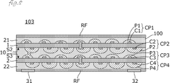
- FIG. 8 is a cross-sectional view of the multilayer substrate 103 according to the third embodiment.
- the multilayer substrate 103 includes a laminate 100 including a first resin base material 1, a second resin base material 2, a bonding layer 10, and coverlays 21 and 22.
- a resist film RF is formed on the surface of the stacked body 100.
- the formation positions of the conductor patterns CP1, CP2, CP3, and CP4 are different from those of the multilayer substrate 101 shown in the first embodiment.
- the other structure is the same as that of the multilayer substrate 101 shown in the first embodiment.
- the first conductor pattern CP1, the second conductor pattern CP2, the third conductor pattern CP3, and the fourth conductor pattern CP4 are arranged at a constant pitch in the cross section in the stacking direction, but the second conductor pattern CP2 Is shifted in the pitch direction with respect to the third conductor pattern CP3. That is, the thickest position (vertex position) of the second conductor pattern CP2 and the thickest position (vertex position) of the third conductor pattern CP3 do not overlap in plan view.
- the rectangular spiral second conductor pattern CP2 and the rectangular spiral third conductor pattern CP3 are arranged so as not to overlap each other in the circumferential direction in plan view. For example, the overlapping ratio is 10% or less.
- the second conductor pattern CP2 and the third conductor pattern CP3 are opposite to each other in the direction inclined to the stacking direction (oblique direction), so that the second surface S2 and the third surface Even if the distance from S3 is narrower, a short circuit between the second conductor pattern CP2 and the third conductor pattern CP3 is prevented.
- FIG. 9 is a diagram showing a mounting structure of a multilayer board 104 according to the fourth embodiment on a circuit board and a mounting method of the multilayer board.
- the pad electrodes 41 and 42 are formed on the circuit board 200, and the solder paste SL is printed on the surface thereof.
- the multilayer substrate 104 is placed on the circuit board 200 with the terminal electrodes 31 and 32 facing the pad electrodes 41 and 42, and the surface opposite to the surface on which the terminal electrodes 31 and 32 are formed is heated and pressed by the hot bar 50.
- the terminal electrodes 31 and 32 are soldered to the pad electrodes 41 and 42.
- the plating film P ⁇ b> 3 of the third conductor pattern formed on the third surface S ⁇ b> 3 of the second resin base material 2 is formed on the second resin base material 2. It is thicker than the plating film P4 of the fourth conductor pattern formed on the fourth surface S4.
- Other configurations are as described in the first embodiment.
- the film thickness of the plating film P2 of the second conductor pattern is the film thickness of the plating film P1 of the first conductor pattern. It should be thinner. Therefore, as in this embodiment, the plating film thickness of the conductor pattern may be in the order of thicker, thinner, thicker, thinner from the top. Moreover, the plating film P4 of the conductor pattern (fourth conductor pattern) on the mounting surface side may be thinner than the plating film P3 of the conductor pattern (third conductor pattern) facing it.
- ⁇ Fifth Embodiment 10 and 11 are views showing the method of manufacturing the multilayer substrate 104 according to the fourth embodiment in the order of the steps.
- the manufacturing method is as follows.
- a photosensitive photoresist film RF1 is applied to the surface of the substrate SUB provided with, for example, a copper foil as a base layer.
- the substrate SUB forms a pattern on both sides at the same time by welding the peripheral portion with ultrasonic waves or bonding them with an adhesive.
- the photosensitive photoresist is exposed by irradiating ultraviolet rays through a photomask. Further, it is possible to draw a fine pattern by directly irradiating the resist with ultraviolet rays using a laser drawing apparatus. Subsequently, the resist film RF1 on the surface of the substrate SUB is developed and patterned.
- a plating film PL11 is deposited in the opening of the resist film RF1 by an electrolytic copper plating method.
- the substrate SUB is separated into two, and the resin layer RL10 is laminated on the one separated substrate SUB so as to embed the plating film PL11.
- the resin layer RL10 is laminated on the other substrate SUB so as to embed the plating film PL21.
- the plating film PL21 is thinner than the plating film PL11.
- the resin layer RL10 of one substrate SUB and the resin layer RL10 of the other substrate SUB are made to face each other and heated and pressed. At this time, since the thin plating film PL11 and the thick plating film PL21 face each other, a short circuit between the plating film PL11 and the plating film PL21 is suppressed.
- the holes H are formed.
- the plating film PL12 is deposited on the exposed plating film PL11.
- the resist film RF is removed and electrolytic copper plating is performed again to deposit the plating film PL22 on the plating film PL21. Further, the thickness of the plating film PL12 is increased.
- a metal catalyst is adsorbed on the inner wall of the hole H, and electrolytic copper plating is performed again to form a plating film on the inner wall of the hole H.
- the multilayer substrate 104 is configured by the above processes. 10 and 11, the resist film RF1 corresponds to the “first resin base material” in the present invention, and the resist film RF2 corresponds to the “second resin base material” in the present invention.
- the resin layer RL10 corresponds to the “bonding layer” in the present invention.
- the plating films PL12, PL11, PL21, and PL22 correspond to the “first conductor pattern”, “second conductor pattern”, “third conductor pattern”, and “fourth conductor pattern” in the present invention, respectively.
- a part of the conductor pattern is embedded in the resin base material.
- the thickness of the conductor pattern embedded in the resin base material (that is, the thickness of the resin base material) also acts as the film thickness of the plating film. Therefore, if the distance between the conductor patterns adjacent to each other in the stacking direction is the same, the cross-sectional area of the conductor pattern can be increased accordingly, and a multilayer substrate having a coil conductor pattern with a small conductor loss can be obtained. Further, if the cross-sectional areas of the conductor patterns are the same, the interval between the conductor patterns adjacent in the stacking direction can be increased.
- FIG. 12 is a diagram illustrating a method of manufacturing the multilayer substrate 105 according to the fifth embodiment in the order of steps. The manufacturing method is as follows.
- the first conductor pattern CP1 and the second conductor pattern CP2 are formed on both surfaces of the first resin base material 1.
- the third conductor pattern CP3 and the fourth conductor pattern CP4 are formed on both surfaces of the second resin base material 2.
- the second conductor pattern CP2 is thinner than the first conductor pattern CP1
- the third conductor pattern CP3 is thinner than the fourth conductor pattern CP4. The method of forming these conductor patterns is as already described in the first embodiment.
- a metal catalyst is adsorbed on the inner wall of the hole H, copper plating is performed, and the inside of the hole H is filled with a plating film. Thereby, an interlayer connection conductor is formed by the plating film in the hole H.
- coverlays 21 and 22 are affixed.
- the multilayer substrate 105 is configured by the above processes. As shown in the present embodiment, the present invention can also be applied to a multilayer substrate including an interlayer connection conductor formed over different resin base materials.
- the conductor pattern formed on both surfaces of the resin base material may be connected at a plurality of locations via interlayer connection conductors. With this structure, since the conductor patterns are connected in parallel in the stacking direction, a multilayer substrate having a conductor pattern with a small conductor loss can be obtained.
- each plating film has been described as being formed by electroplating, but these plating films may be formed by electroless plating.
- each conductor pattern may not be formed with a plating film but may be polished by a predetermined thickness and then the thickness may be made uniform.
- the materials such as the resin base materials 1 and 2 are described as liquid crystal polymers, but these may be polyimide resins.
- the bonding layer 10 may be a polyimide resin in addition to the epoxy resin.
- the bonding layer has higher fluidity than the resin base material at the pressing temperature.
- a resin material containing glass fiber can be used as the bonding layer.
- the first conductor pattern is not limited to the one present in the outermost layer among the plurality of conductor patterns formed in the plurality of layers in the multilayer body. Even if there is another resin substrate closer to the outermost layer than the first resin substrate, and the conductor pattern is formed on the resin substrate, the conductor pattern faces the first conductor pattern via the bonding layer. If you don't,
- the multilayer substrate of the present invention is not limited to a coil device, but can be applied to various electronic components such as an antenna, an actuator, and a sensor.
- the multilayer substrate of the present invention includes chip components such as a chip inductor formed into a chip.
- the present invention can be modified as appropriate without departing from the spirit of the present invention.
Landscapes
- Engineering & Computer Science (AREA)
- Power Engineering (AREA)
- Microelectronics & Electronic Packaging (AREA)
- Manufacturing & Machinery (AREA)
- Production Of Multi-Layered Print Wiring Board (AREA)
- Parts Printed On Printed Circuit Boards (AREA)
Abstract
La présente invention concerne un substrat multicouche (101) qui comprend un corps stratifié obtenu par pression à chaud d'un premier matériau de base en résine (1), d'un deuxième matériau de base en résine (2), et d'une couche de soudage (10). Un premier motif conducteur (CP1) ayant une pellicule de placage sur sa surface est formé sur une première surface (S1) du premier matériau de base en résine (1). Un deuxième motif conducteur (CP2) ayant une pellicule de placage sur sa surface est formé sur une deuxième surface (S2). Un troisième motif conducteur (CP3) ayant une pellicule de placage sur sa surface est formé sur une troisième surface (S3) du deuxième matériau de base en résine (2). Un quatrième motif conducteur (CP4) ayant une pellicule de placage sur sa surface est formé sur une quatrième surface (S4). Le premier motif conducteur (CP1) est positionné plus près de la couche la plus extérieure que le deuxième motif conducteur (CP2). Le deuxième motif conducteur (CP2) est plus mince que le premier motif conducteur (CP1).
Priority Applications (3)
| Application Number | Priority Date | Filing Date | Title |
|---|---|---|---|
| JP2018518528A JP6380716B1 (ja) | 2016-11-28 | 2017-11-21 | 多層基板、多層基板の回路基板への実装構造、および多層基板の製造方法 |
| CN201790000777.5U CN209449029U (zh) | 2016-11-28 | 2017-11-21 | 多层基板以及多层基板向电路基板的安装构造 |
| US16/158,334 US10893618B2 (en) | 2016-11-28 | 2018-10-12 | Method for manufacturing multilayer substrate |
Applications Claiming Priority (2)
| Application Number | Priority Date | Filing Date | Title |
|---|---|---|---|
| JP2016229706 | 2016-11-28 | ||
| JP2016-229706 | 2016-11-28 |
Related Child Applications (1)
| Application Number | Title | Priority Date | Filing Date |
|---|---|---|---|
| US16/158,334 Continuation US10893618B2 (en) | 2016-11-28 | 2018-10-12 | Method for manufacturing multilayer substrate |
Publications (1)
| Publication Number | Publication Date |
|---|---|
| WO2018097112A1 true WO2018097112A1 (fr) | 2018-05-31 |
Family
ID=62195166
Family Applications (1)
| Application Number | Title | Priority Date | Filing Date |
|---|---|---|---|
| PCT/JP2017/041737 Ceased WO2018097112A1 (fr) | 2016-11-28 | 2017-11-21 | Substrat multicouche, structure de montage de substrat multicouche sur carte de circuit imprimé, procédé de montage de substrat multicouche, et procédé de production de substrat multicouche |
Country Status (4)
| Country | Link |
|---|---|
| US (1) | US10893618B2 (fr) |
| JP (1) | JP6380716B1 (fr) |
| CN (1) | CN209449029U (fr) |
| WO (1) | WO2018097112A1 (fr) |
Cited By (4)
| Publication number | Priority date | Publication date | Assignee | Title |
|---|---|---|---|---|
| KR20210148757A (ko) * | 2020-06-01 | 2021-12-08 | 동의대학교 산학협력단 | 디지털 콘덴서가 장착된 다중 웨이퍼의 결합구조 및 제조방법 |
| JP2022507980A (ja) * | 2018-11-26 | 2022-01-18 | ハッチンソン テクノロジー インコーポレイテッド | 高アスペクト比電気メッキ構造および異方性電気メッキ処理 |
| US12308157B2 (en) | 2016-11-18 | 2025-05-20 | Hutchinson Technology Incorporated | High density coil design and process |
| US12378687B2 (en) | 2016-11-18 | 2025-08-05 | Hutchinson Technology Incorporated | High aspect ratio electroplated structures and anisotropic electroplating processes |
Families Citing this family (3)
| Publication number | Priority date | Publication date | Assignee | Title |
|---|---|---|---|---|
| JP7323268B2 (ja) * | 2018-03-16 | 2023-08-08 | 日東電工株式会社 | 磁性配線回路基板およびその製造方法 |
| WO2020067427A1 (fr) * | 2018-09-27 | 2020-04-02 | デンカ株式会社 | Substrat lié, circuit imprimé métallique et circuit imprimé |
| CN115516585A (zh) * | 2022-03-28 | 2022-12-23 | 英麦科磁集成科技有限公司 | 线圈电感器及其制造方法 |
Citations (9)
| Publication number | Priority date | Publication date | Assignee | Title |
|---|---|---|---|---|
| JPH02161709A (ja) * | 1988-12-15 | 1990-06-21 | Mitsui Mining & Smelting Co Ltd | 多層プリントシートコイルの製造方法 |
| JPH04368105A (ja) * | 1991-06-17 | 1992-12-21 | Toshiba Corp | 平面インダクタ |
| JPH06217482A (ja) * | 1993-12-01 | 1994-08-05 | Sony Corp | 回路パターン形成方法 |
| JPH09232162A (ja) * | 1995-12-19 | 1997-09-05 | Murata Mfg Co Ltd | 多層基板 |
| JPH10163028A (ja) * | 1996-11-26 | 1998-06-19 | Murata Mfg Co Ltd | 積層コイル装置 |
| JP2006041418A (ja) * | 2004-07-30 | 2006-02-09 | Toko Inc | 面実装コイル部品 |
| JP2008205353A (ja) * | 2007-02-22 | 2008-09-04 | Kyocera Corp | コイル内蔵基板 |
| JP2008306007A (ja) * | 2007-06-08 | 2008-12-18 | Nec Corp | インダクタ、配線基板、および半導体装置 |
| JP2010010550A (ja) * | 2008-06-30 | 2010-01-14 | Kyocera Corp | 電子部品の実装構造 |
Family Cites Families (19)
| Publication number | Priority date | Publication date | Assignee | Title |
|---|---|---|---|---|
| US6911887B1 (en) * | 1994-09-12 | 2005-06-28 | Matsushita Electric Industrial Co., Ltd. | Inductor and method for producing the same |
| JP3642110B2 (ja) * | 1996-06-11 | 2005-04-27 | 松下電器産業株式会社 | 電子部品の製造方法 |
| US5942965A (en) * | 1996-09-13 | 1999-08-24 | Murata Manufacturing Co., Ltd. | Multilayer substrate |
| JP3500319B2 (ja) * | 1998-01-08 | 2004-02-23 | 太陽誘電株式会社 | 電子部品 |
| JP3446681B2 (ja) * | 1999-09-28 | 2003-09-16 | 株式会社村田製作所 | 積層インダクタアレイ |
| JP2002134319A (ja) * | 2000-10-23 | 2002-05-10 | Alps Electric Co Ltd | スパイラルインダクタ |
| JP4214700B2 (ja) * | 2002-01-22 | 2009-01-28 | 株式会社村田製作所 | コモンモードチョークコイルアレイ |
| JP4191506B2 (ja) * | 2003-02-21 | 2008-12-03 | Tdk株式会社 | 高密度インダクタおよびその製造方法 |
| JP4317470B2 (ja) * | 2004-02-25 | 2009-08-19 | Tdk株式会社 | コイル部品及びその製造方法 |
| KR100716848B1 (ko) * | 2005-10-17 | 2007-05-09 | 주식회사 팬택앤큐리텔 | 가변 인덕턴스를 갖는 나선형 인덕터 |
| KR100993413B1 (ko) * | 2005-11-01 | 2010-11-09 | 도시바 마테리알 가부시키가이샤 | 평면 자기 소자 및 그것을 이용한 전원 ic 패키지 |
| JP2007250924A (ja) * | 2006-03-17 | 2007-09-27 | Sony Corp | インダクタ素子とその製造方法、並びにインダクタ素子を用いた半導体モジュール |
| TW201001457A (en) * | 2008-06-30 | 2010-01-01 | Delta Electronics Inc | Magnetic component |
| TW201011788A (en) * | 2008-09-04 | 2010-03-16 | Delta Electronics Inc | Magnetic element |
| JP4714779B2 (ja) * | 2009-04-10 | 2011-06-29 | 東光株式会社 | 表面実装インダクタの製造方法とその表面実装インダクタ |
| JP5874199B2 (ja) | 2011-05-26 | 2016-03-02 | Tdk株式会社 | コイル部品及びその製造方法 |
| KR101434351B1 (ko) * | 2010-10-21 | 2014-08-26 | 티디케이가부시기가이샤 | 코일 부품 및 그 제조 방법 |
| KR101514491B1 (ko) * | 2011-12-08 | 2015-04-23 | 삼성전기주식회사 | 코일 부품 및 그 제조방법 |
| US9009951B2 (en) * | 2012-04-24 | 2015-04-21 | Cyntec Co., Ltd. | Method of fabricating an electromagnetic component |
-
2017
- 2017-11-21 WO PCT/JP2017/041737 patent/WO2018097112A1/fr not_active Ceased
- 2017-11-21 CN CN201790000777.5U patent/CN209449029U/zh active Active
- 2017-11-21 JP JP2018518528A patent/JP6380716B1/ja active Active
-
2018
- 2018-10-12 US US16/158,334 patent/US10893618B2/en active Active
Patent Citations (9)
| Publication number | Priority date | Publication date | Assignee | Title |
|---|---|---|---|---|
| JPH02161709A (ja) * | 1988-12-15 | 1990-06-21 | Mitsui Mining & Smelting Co Ltd | 多層プリントシートコイルの製造方法 |
| JPH04368105A (ja) * | 1991-06-17 | 1992-12-21 | Toshiba Corp | 平面インダクタ |
| JPH06217482A (ja) * | 1993-12-01 | 1994-08-05 | Sony Corp | 回路パターン形成方法 |
| JPH09232162A (ja) * | 1995-12-19 | 1997-09-05 | Murata Mfg Co Ltd | 多層基板 |
| JPH10163028A (ja) * | 1996-11-26 | 1998-06-19 | Murata Mfg Co Ltd | 積層コイル装置 |
| JP2006041418A (ja) * | 2004-07-30 | 2006-02-09 | Toko Inc | 面実装コイル部品 |
| JP2008205353A (ja) * | 2007-02-22 | 2008-09-04 | Kyocera Corp | コイル内蔵基板 |
| JP2008306007A (ja) * | 2007-06-08 | 2008-12-18 | Nec Corp | インダクタ、配線基板、および半導体装置 |
| JP2010010550A (ja) * | 2008-06-30 | 2010-01-14 | Kyocera Corp | 電子部品の実装構造 |
Cited By (6)
| Publication number | Priority date | Publication date | Assignee | Title |
|---|---|---|---|---|
| US12308157B2 (en) | 2016-11-18 | 2025-05-20 | Hutchinson Technology Incorporated | High density coil design and process |
| US12378687B2 (en) | 2016-11-18 | 2025-08-05 | Hutchinson Technology Incorporated | High aspect ratio electroplated structures and anisotropic electroplating processes |
| JP2022507980A (ja) * | 2018-11-26 | 2022-01-18 | ハッチンソン テクノロジー インコーポレイテッド | 高アスペクト比電気メッキ構造および異方性電気メッキ処理 |
| JP7494177B2 (ja) | 2018-11-26 | 2024-06-03 | ハッチンソン テクノロジー インコーポレイテッド | 電気メッキ構造 |
| KR20210148757A (ko) * | 2020-06-01 | 2021-12-08 | 동의대학교 산학협력단 | 디지털 콘덴서가 장착된 다중 웨이퍼의 결합구조 및 제조방법 |
| KR102387562B1 (ko) * | 2020-06-01 | 2022-04-15 | 동의대학교 산학협력단 | 디지털 콘덴서가 장착된 다중 웨이퍼의 결합구조 및 제조방법 |
Also Published As
| Publication number | Publication date |
|---|---|
| US10893618B2 (en) | 2021-01-12 |
| US20190082542A1 (en) | 2019-03-14 |
| JP6380716B1 (ja) | 2018-08-29 |
| CN209449029U (zh) | 2019-09-27 |
| JPWO2018097112A1 (ja) | 2018-12-06 |
Similar Documents
| Publication | Publication Date | Title |
|---|---|---|
| JP6380716B1 (ja) | 多層基板、多層基板の回路基板への実装構造、および多層基板の製造方法 | |
| CN101978799B (zh) | 印刷电路板及其制造方法 | |
| CN1671274B (zh) | 具有层间接合部位的柔性基板及其制造方法 | |
| JP6380715B1 (ja) | 多層基板、多層基板の回路基板への実装構造、多層基板の実装方法および多層基板の製造方法 | |
| JP2003023250A (ja) | 多層基板のおよびその製造方法 | |
| CN101896037A (zh) | 刚挠性电路板及其制造方法 | |
| TW201410097A (zh) | 柔性多層電路板及其製作方法 | |
| US11456108B2 (en) | Multilayer board and manufacturing method thereof | |
| US10477704B2 (en) | Multilayer board and electronic device | |
| US20160135295A1 (en) | Multi-layer circuit board | |
| US20170006699A1 (en) | Multilayer circuit board, semiconductor apparatus, and method of manufacturing multilayer circuit board | |
| US11688553B2 (en) | Multilayer coil and method for manufacturing the same | |
| JP2004088093A (ja) | 多層回路基板の形成方法および多層回路基板 | |
| CN101022695B (zh) | 线路嵌合于介电层的无芯板薄型基板及其制造方法 | |
| JP2004031476A (ja) | 電子部品内蔵多層プリント基板及びその製造方法 | |
| JP2616588B2 (ja) | ポリイミド多層配線基板およびその製造方法 | |
| WO2021025025A1 (fr) | Substrat multicouche en résine et procédé de production de substrat multicouche en résine | |
| WO2020203724A1 (fr) | Substrat multicouche en résine et procédé de production de substrat multicouche en résine | |
| JP2020088197A (ja) | 樹脂多層基板および電子機器 | |
| JP4892924B2 (ja) | 多層プリント配線基板及びその製造方法 | |
| JP4821276B2 (ja) | 多層プリント配線板の製造方法及び多層プリント配線板 | |
| JP2001144445A (ja) | 多層プリント配線板の製造方法 | |
| JP2017204490A (ja) | 部品実装基板、および、部品実装基板の製造方法 | |
| JP3867526B2 (ja) | 多層基板の製造方法 | |
| CN117279232A (zh) | 线路板及其制作方法 |
Legal Events
| Date | Code | Title | Description |
|---|---|---|---|
| ENP | Entry into the national phase |
Ref document number: 2018518528 Country of ref document: JP Kind code of ref document: A |
|
| 121 | Ep: the epo has been informed by wipo that ep was designated in this application |
Ref document number: 17874702 Country of ref document: EP Kind code of ref document: A1 |
|
| NENP | Non-entry into the national phase |
Ref country code: DE |
|
| 122 | Ep: pct application non-entry in european phase |
Ref document number: 17874702 Country of ref document: EP Kind code of ref document: A1 |