WO2018116746A1 - Soiウェーハの製造方法 - Google Patents
Soiウェーハの製造方法 Download PDFInfo
- Publication number
- WO2018116746A1 WO2018116746A1 PCT/JP2017/042334 JP2017042334W WO2018116746A1 WO 2018116746 A1 WO2018116746 A1 WO 2018116746A1 JP 2017042334 W JP2017042334 W JP 2017042334W WO 2018116746 A1 WO2018116746 A1 WO 2018116746A1
- Authority
- WO
- WIPO (PCT)
- Prior art keywords
- wafer
- bonding
- drying
- bond
- soi
- Prior art date
- Legal status (The legal status is an assumption and is not a legal conclusion. Google has not performed a legal analysis and makes no representation as to the accuracy of the status listed.)
- Ceased
Links
Images

Classifications
-
- H—ELECTRICITY
- H10—SEMICONDUCTOR DEVICES; ELECTRIC SOLID-STATE DEVICES NOT OTHERWISE PROVIDED FOR
- H10P—GENERIC PROCESSES OR APPARATUS FOR THE MANUFACTURE OR TREATMENT OF DEVICES COVERED BY CLASS H10
- H10P90/00—Preparation of wafers not covered by a single main group of this subclass, e.g. wafer reinforcement
- H10P90/19—Preparing inhomogeneous wafers
- H10P90/1904—Preparing vertically inhomogeneous wafers
- H10P90/1906—Preparing SOI wafers
-
- H—ELECTRICITY
- H10—SEMICONDUCTOR DEVICES; ELECTRIC SOLID-STATE DEVICES NOT OTHERWISE PROVIDED FOR
- H10P—GENERIC PROCESSES OR APPARATUS FOR THE MANUFACTURE OR TREATMENT OF DEVICES COVERED BY CLASS H10
- H10P90/00—Preparation of wafers not covered by a single main group of this subclass, e.g. wafer reinforcement
- H10P90/19—Preparing inhomogeneous wafers
- H10P90/1904—Preparing vertically inhomogeneous wafers
- H10P90/1906—Preparing SOI wafers
- H10P90/1914—Preparing SOI wafers using bonding
-
- H—ELECTRICITY
- H10—SEMICONDUCTOR DEVICES; ELECTRIC SOLID-STATE DEVICES NOT OTHERWISE PROVIDED FOR
- H10D—INORGANIC ELECTRIC SEMICONDUCTOR DEVICES
- H10D86/00—Integrated devices formed in or on insulating or conducting substrates, e.g. formed in silicon-on-insulator [SOI] substrates or on stainless steel or glass substrates
-
- H—ELECTRICITY
- H10—SEMICONDUCTOR DEVICES; ELECTRIC SOLID-STATE DEVICES NOT OTHERWISE PROVIDED FOR
- H10P—GENERIC PROCESSES OR APPARATUS FOR THE MANUFACTURE OR TREATMENT OF DEVICES COVERED BY CLASS H10
- H10P14/00—Formation of materials, e.g. in the shape of layers or pillars
- H10P14/20—Formation of materials, e.g. in the shape of layers or pillars of semiconductor materials
- H10P14/29—Formation of materials, e.g. in the shape of layers or pillars of semiconductor materials characterised by the substrates
- H10P14/2901—Materials
- H10P14/2902—Materials being Group IVA materials
- H10P14/2905—Silicon, silicon germanium or germanium
-
- H—ELECTRICITY
- H10—SEMICONDUCTOR DEVICES; ELECTRIC SOLID-STATE DEVICES NOT OTHERWISE PROVIDED FOR
- H10P—GENERIC PROCESSES OR APPARATUS FOR THE MANUFACTURE OR TREATMENT OF DEVICES COVERED BY CLASS H10
- H10P14/00—Formation of materials, e.g. in the shape of layers or pillars
- H10P14/60—Formation of materials, e.g. in the shape of layers or pillars of insulating materials
- H10P14/65—Formation of materials, e.g. in the shape of layers or pillars of insulating materials characterised by treatments performed before or after the formation of the materials
- H10P14/6516—Formation of materials, e.g. in the shape of layers or pillars of insulating materials characterised by treatments performed before or after the formation of the materials of treatments performed after formation of the materials
- H10P14/6529—Formation of materials, e.g. in the shape of layers or pillars of insulating materials characterised by treatments performed before or after the formation of the materials of treatments performed after formation of the materials by exposure to a gas or vapour
- H10P14/6532—Formation of materials, e.g. in the shape of layers or pillars of insulating materials characterised by treatments performed before or after the formation of the materials of treatments performed after formation of the materials by exposure to a gas or vapour by exposure to a plasma
-
- H—ELECTRICITY
- H10—SEMICONDUCTOR DEVICES; ELECTRIC SOLID-STATE DEVICES NOT OTHERWISE PROVIDED FOR
- H10P—GENERIC PROCESSES OR APPARATUS FOR THE MANUFACTURE OR TREATMENT OF DEVICES COVERED BY CLASS H10
- H10P14/00—Formation of materials, e.g. in the shape of layers or pillars
- H10P14/60—Formation of materials, e.g. in the shape of layers or pillars of insulating materials
- H10P14/69—Inorganic materials
- H10P14/6903—Inorganic materials containing silicon
-
- H—ELECTRICITY
- H10—SEMICONDUCTOR DEVICES; ELECTRIC SOLID-STATE DEVICES NOT OTHERWISE PROVIDED FOR
- H10P—GENERIC PROCESSES OR APPARATUS FOR THE MANUFACTURE OR TREATMENT OF DEVICES COVERED BY CLASS H10
- H10P70/00—Cleaning of wafers, substrates or parts of devices
- H10P70/10—Cleaning before device manufacture, i.e. Begin-Of-Line process
- H10P70/12—Cleaning before device manufacture, i.e. Begin-Of-Line process by dry cleaning only
-
- H—ELECTRICITY
- H10—SEMICONDUCTOR DEVICES; ELECTRIC SOLID-STATE DEVICES NOT OTHERWISE PROVIDED FOR
- H10P—GENERIC PROCESSES OR APPARATUS FOR THE MANUFACTURE OR TREATMENT OF DEVICES COVERED BY CLASS H10
- H10P70/00—Cleaning of wafers, substrates or parts of devices
- H10P70/10—Cleaning before device manufacture, i.e. Begin-Of-Line process
- H10P70/15—Cleaning before device manufacture, i.e. Begin-Of-Line process by wet cleaning only
-
- H—ELECTRICITY
- H10—SEMICONDUCTOR DEVICES; ELECTRIC SOLID-STATE DEVICES NOT OTHERWISE PROVIDED FOR
- H10P—GENERIC PROCESSES OR APPARATUS FOR THE MANUFACTURE OR TREATMENT OF DEVICES COVERED BY CLASS H10
- H10P95/00—Generic processes or apparatus for manufacture or treatments not covered by the other groups of this subclass
-
- H—ELECTRICITY
- H10—SEMICONDUCTOR DEVICES; ELECTRIC SOLID-STATE DEVICES NOT OTHERWISE PROVIDED FOR
- H10P—GENERIC PROCESSES OR APPARATUS FOR THE MANUFACTURE OR TREATMENT OF DEVICES COVERED BY CLASS H10
- H10P95/00—Generic processes or apparatus for manufacture or treatments not covered by the other groups of this subclass
- H10P95/90—Thermal treatments, e.g. annealing or sintering
-
- H—ELECTRICITY
- H10—SEMICONDUCTOR DEVICES; ELECTRIC SOLID-STATE DEVICES NOT OTHERWISE PROVIDED FOR
- H10W—GENERIC PACKAGES, INTERCONNECTIONS, CONNECTORS OR OTHER CONSTRUCTIONAL DETAILS OF DEVICES COVERED BY CLASS H10
- H10W10/00—Isolation regions in semiconductor bodies between components of integrated devices
- H10W10/10—Isolation regions comprising dielectric materials
- H10W10/181—Semiconductor-on-insulator [SOI] isolation regions, e.g. buried oxide regions of SOI wafers
Definitions
- the present invention relates to an SOI wafer manufacturing method, and more particularly, to an SOI wafer manufacturing method by bonding two wafers.
- outer peripheral portion is minute.
- outer microvoids When two silicon wafers are bonded together at room temperature, at the end of bonding progressing from one of the outer peripheral edges of the wafer to the outer peripheral edge on the opposite side, an air residue is generated due to the wraparound of the bonding, and the outer peripheral portion is minute. In some cases (hereinafter referred to as outer microvoids).
- the outer peripheral microvoids are formed in a size of about 0.1 to 1 mm in diameter within a range of 3 to 5 mm from the edge of the outer periphery of the wafer, and tend to increase as the bonding speed at the time of bonding increases.
- the bonding between the wafers spreads across the entire surface due to the attractive force acting between the high-precision surfaces with small roughness. By observing with, etc., the bonding speed can be measured.
- plasma processing processing that activates the surface to be bonded by exposure to plasma
- plasma processing is performed on the surfaces to be bonded, which increases the bonding speed and generates minute voids on the periphery. It becomes easy to do.
- Patent Document 1 describes that “edge voids”, which are voids appearing on the outer periphery of a bonded wafer, can be suppressed at a bonding speed of less than 1.7 cm / s.
- Patent Document 2 [0005] [0006] describes that minute voids on the outer periphery of the wafer can be suppressed by setting the contact wave speed to 50 mm / second or less.
- Patent Document 1 discloses that the layer thickness of water adsorbed on the wafer surface is reduced by heating, and Patent Document 2 describes the progress of bonding by controlling the pressure, type, and viscosity of the atmosphere in the bonding environment. Although it is described that the speed is controlled, these are not simple methods.
- an object of the present invention is to provide an SOI wafer manufacturing method capable of manufacturing an SOI wafer while suppressing the generation of outer peripheral microvoids by a simple method.
- the present invention provides a silicon oxide film in which a bond wafer made of a silicon wafer and a base wafer made of a silicon wafer are formed on at least one surface of the bond wafer and the base wafer.
- the manufacturing method of an SOI wafer for manufacturing an SOI wafer including a bonding step of bonding at room temperature via a thin film and a thinning step of thinning the bond wafer after the bonding step, than the bonding step Before, further, a cleaning step of cleaning the bond wafer and the base wafer with a hydrophilic cleaning liquid, and at least one of suction drying and spin drying of the bond wafer and the base wafer after the cleaning is performed.
- a drying step of drying by one drying method The bonding wafer and the base wafer are stored until the bonding speed at the time of performing the bonding process is 20 mm / second or less after the end of the process and before the bonding process is started.
- a method for manufacturing an SOI wafer wherein the bonding is performed at a speed of 20 mm / second or less.
- the storage time is preferably 70 minutes or more.
- Such a storage time makes it easy to control the bonding speed at the time of bonding to 20 mm / second or less. As a result, it is possible to manufacture the SOI wafer while more reliably suppressing the generation of outer peripheral microvoids.
- a plasma treatment may be performed on at least one of the bond wafer and the base wafer.
- the bonding strength between the wafers at the time of bonding can be increased.
- the bonding speed at the time of bonding tends to be higher than when the plasma treatment is not performed, and the outer peripheral microvoids are likely to be generated.
- the present invention is particularly effective when performing plasma processing that easily generates outer peripheral microvoids.
- the hydrophilic cleaning liquid is an SC1 solution or an SC2 solution.
- an SC1 solution or an SC2 solution can be suitably used as the hydrophilic cleaning liquid used for cleaning the wafer before bonding.
- the storage time is preferably 5 hours or less.
- the bond wafer and the base wafer so as to be in contact with an atmosphere having a temperature of 25 ⁇ 5 ° C. and a humidity of 40 ⁇ 20%.
- This kind of atmosphere is similar to the atmosphere in a normal clean room. By storing the wafer in contact with such an atmosphere, moisture on the wafer surface can be reduced to an appropriate range.
- the bond wafer and the base wafer may be left in a state of being bonded for 24 hours or more before the first heat treatment after the bonding step. preferable.
- the outer peripheral microvoids can be simply adjusted by adjusting the storage time from the end of the drying process to the start of the bonding process.
- the SOI wafer can be manufactured while suppressing the occurrence of the above. Therefore, it does not involve capital investment by introducing new equipment or remodeling conventional equipment, so that it is an inexpensive method.
- the method for manufacturing an SOI wafer according to the present invention includes a bond wafer made of a silicon wafer and a base wafer made of a silicon wafer at room temperature via a silicon oxide film formed on at least one surface of the bond wafer and the base wafer. And a bonding step of bonding together. Moreover, it has the thin film formation process which thins a bond wafer after this bonding process.
- a cleaning step of cleaning the bond wafer and the base wafer with a hydrophilic cleaning liquid, and the bond wafer and the base wafer after the cleaning are sucked and dried. And a drying step of drying by at least any one of the spin drying methods.
- the bond wafer and the base wafer are stored until the bonding speed at the time of performing the bonding process becomes 20 mm / second or less before the bonding process is started after the completion of the drying process. After such storage, the bonding is performed at a bonding speed of 20 mm / second or less.
- the suction drying method and the spin drying method are close to natural drying, there is a lot of moisture on the silicon wafer surface even after the drying process is completed.
- bonding at room temperature is performed by water hydrogen bonding, so that the bonding speed increases when the amount of moisture on the wafer surface is large.
- the moisture on the wafer surface decreases to an amount suitable for the humidity of the environment. As a result, the bonding speed is lowered, and the number of generated outer peripheral microvoids can be reduced, or can be reduced to zero.
- Patent Documents 1 and 2 As described above, it is known that the bonding speed is lowered in order to suppress outer peripheral microvoids (Patent Documents 1 and 2).
- Patent Document 1 discloses that the layer thickness of water adsorbed on the surface is reduced by heating
- Patent Document 2 describes a bonding environment (atmosphere, pressure, etc.).
- it does not describe controlling the elapsed time (storage time) from washing and drying to bonding, as in the present invention.
- FIG. 1 is a flowchart showing an outline of the steps (a to g) of the present invention.
- a bond wafer made of a silicon wafer and a base wafer made of a silicon wafer are prepared (step a). At this time, at least one of the bond wafer and the base wafer is prepared with a silicon oxide film formed on the surface.
- the surface silicon oxide film is preferably a thermal oxide film.
- the bond wafer and the base wafer prepared as described above are cleaned (step c). Before that, it is preferable to perform plasma treatment on at least one of the bond wafer and the base wafer (step b). .
- This step is not essential.
- This plasma treatment is a treatment for activating the surface to which the wafer is bonded by being exposed to plasma. By this plasma treatment, the bonding strength of the bonded wafer after bonding the wafers can be increased. However, in this plasma processing, the bonding speed at the time of bonding tends to be higher than when plasma processing is not performed, and peripheral voids are likely to be generated.
- the storage time after the drying step can be adjusted to reduce the bonding speed, thereby suppressing the generation of outer peripheral microvoids.
- step c the bond wafer and the base wafer are cleaned with a hydrophilic cleaning solution.
- This washing is preferably performed with an SC1 solution or an SC2 solution.
- the SC1 solution is an aqueous solution containing ammonia and hydrogen peroxide
- the SC2 solution is an aqueous solution containing hydrogen chloride and hydrogen peroxide, both of which have a composition that is usually used for cleaning silicon wafers.
- the conditions normally used in the cleaning of the silicon wafer can be applied to other cleaning conditions.
- the bond wafer and the base wafer after the cleaning are dried by at least one drying method of suction drying and spin drying (step d).
- suction drying or spin drying reference can be made, for example, to JP-A-2002-313689.
- Suction drying is a drying method in which moisture on the wafer surface is removed by suction.
- the water on the wafer surface can be removed by placing the silicon wafer almost vertically on a drying base provided with a vacuum suction line and sucking the water from the lower part of the wafer.
- IPA drying water displacement method
- the present invention includes a storage step (step e).
- the bond wafer and the base wafer are stored until the bonding speed when performing the bonding process is 20 mm / second or less.
- the bonding speed can be measured by observing with an infrared camera or the like. Both suction drying and spin drying can leave moisture on the wafer surface and adjust the amount of moisture at the time of bonding. Conventionally, when bonding is performed immediately after suction drying or spin drying, as described above, The bonding speed was too high, and the outer peripheral microvoids could not be suppressed.
- the length of the storage time in the storage step is not particularly limited as long as the bonding speed at the time of bonding can be 20 mm / second or less, but is preferably 50 minutes or more, and particularly preferably 70 minutes or more.
- the bond wafer and the base wafer are preferably stored in contact with an atmosphere having a temperature of 25 ⁇ 5 ° C. and a humidity of 40 ⁇ 20%. Such an atmosphere is similar to the atmosphere in a normal clean room. By storing the wafer in contact with such an atmosphere, moisture on the wafer surface can be reduced to an appropriate range. In consideration of productivity, the storage time is preferably 5 hours or less.
- step f the bond wafer and the base wafer are bonded together at room temperature via a silicon oxide film formed on at least one surface of the bond wafer and the base wafer.
- the bonding speed is 20 mm / second or less, and the generation of outer peripheral microvoids is suppressed.
- a thinning step for thinning the bond wafer is performed (step g).
- This thinning may be performed by ion implantation separation or by techniques such as grinding, polishing, and etching.
- an ion implantation layer such as hydrogen ions is provided on the bond wafer in advance before at least the cleaning step (step c).
- heat treatment peeling heat treatment
- the bond wafer can be thinned by performing peeling at the ion implantation layer.
- a bonding heat treatment can be performed after the separation heat treatment or in combination with the separation heat treatment.
- the bonding strength of the bonded wafer can be increased.
- thinning is performed by grinding, polishing, etching, or the like
- the SOI wafer is manufactured as described above, steps other than those described above may be provided.
- steps other than those described above may be provided.
- a silicon single crystal wafer having a diameter of 300 mm and a crystal orientation ⁇ 100> of the main surface was prepared.
- a thermal oxide film was formed with a thickness of 190 nm. Hydrogen ion implantation for peeling was performed on this bond wafer to form a hydrogen ion implanted layer.
- a silicon single crystal wafer having a diameter of 300 mm and a crystal orientation ⁇ 100> of the main surface was prepared. No thermal oxide film was formed on this base wafer, and no hydrogen ion implanted layer was formed.
- plasma treatment was performed on both the bond wafer and the base wafer.
- the plasma treatment was performed with oxygen plasma.
- the storage was performed in a wafer container FOUP (Front-Opening Unified Pod).
- the storage environment was a temperature of 22 ° C. and a humidity of 40%. This was an atmosphere equivalent to the atmosphere in the clean room.
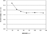
- the storage time in this storage process was changed in the range of 18 minutes to 130 minutes.
- bonding was performed at room temperature. After bonding, peeling heat treatment was performed at 500 ° C. for 30 minutes, and peeling was performed with a hydrogen ion implanted layer.
- Void observation was performed after completion of peeling. Specifically, the bonded wafer after peeling was visually observed under a fluorescent lamp or a condenser lamp.
- the relationship between the storage time after the drying process and the bonding speed is shown in FIG. From FIG. 2, it was found that the bonding speed became slower than 20 mm / second when the storage time exceeded about 50 minutes, and almost saturated at about 19.5 mm / second when the storage time was 70 minutes or more.
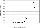
- the bonding speed is changed by changing the surface roughness after cleaning, and the bonding speed and one wafer are changed.
- the relationship with the number of perimeter microvoids generated per hit was investigated, and the results are shown in FIG. It was found that when the bonding speed was about 20 mm / sec or less, the outer peripheral microvoids were hardly generated.
- the bonding speed was calculated from the time and the wafer diameter by observing the coupled wave with an infrared camera, measuring the time during which the coupled wave traveled from one end of the wafer to the opposite end.
- Example 1 One batch (25 sheets) of bonded SOI wafers were produced under the same conditions as in the experimental example except that the elapsed time (storage time) until bonding at room temperature was 70 minutes after completion of the drying step. At this time, since the 25 sheets were bonded together, the storage time for the first sheet was 70 minutes, but the storage time for the 25th sheet was 120 minutes. That is, the storage time is varied in the range of 70 minutes to 120 minutes. At that time, the bonding speed was in the range of 19.0 to 19.5 mm / sec. As a result, the average number of outer peripheral microvoids was 0.8 / sheet.
- Example 2 One batch (25 sheets) of bonded SOI wafers were manufactured under the same conditions as in the experimental example, except that the storage time until the bonding at room temperature was performed after the drying process was 50 minutes. At this time, as in Example 1, 25 sheets were continuously bonded. Accordingly, the storage time for the first sheet was 50 minutes, but the elapsed time for the 25th sheet was 100 minutes. That is, the storage time is varied in the range of 50 minutes to 100 minutes. At that time, the bonding speed was in the range of 19.5 to 20.0 mm / sec. As a result, the average number of outer peripheral microvoids was 4.8 / sheet.
- Example 3 One batch (25 sheets) of bonded SOI wafers was produced under the same conditions as in Example 1 except that the wafer immediately after being bonded at room temperature was left for one day (24 hours) at room temperature and then was subjected to peeling heat treatment. did. As a result, the average number of outer peripheral microvoids was 0.08 / sheet.
- Example 4 One batch (25 sheets) of bonded SOI wafers were produced under the same conditions as in Example 2 except that the wafer immediately after being bonded at room temperature was left as it was at room temperature for 4 days and then the heat treatment for peeling was performed. As a result, the average number of outer peripheral microvoids was 0.2 / sheet.
- the present invention is not limited to the above embodiment.
- the above-described embodiment is an exemplification, and the present invention has substantially the same configuration as the technical idea described in the claims of the present invention, and any device that exhibits the same function and effect is the present invention. It is included in the technical scope of the invention.
Landscapes
- Pressure Welding/Diffusion-Bonding (AREA)
- Cleaning Or Drying Semiconductors (AREA)
- Physics & Mathematics (AREA)
- Engineering & Computer Science (AREA)
- Plasma & Fusion (AREA)
- Container, Conveyance, Adherence, Positioning, Of Wafer (AREA)
- Crystals, And After-Treatments Of Crystals (AREA)
Abstract
本発明は、ともにシリコンウェーハからなるボンドウェーハとベースウェーハとを、シリコン酸化膜を介して室温で貼り合わせる工程と、ボンドウェーハを薄膜化する工程とを有し、貼り合わせ工程よりも前に、両ウェーハを親水性の洗浄液で洗浄する工程と、洗浄後の両ウェーハを、吸引乾燥又はスピン乾燥で乾燥する工程とを有し、乾燥工程の終了後、貼り合わせ工程を開始するまでの間に、貼り合わせ工程を行う際の貼り合わせ速度が20mm/秒以下になるまで両ウェーハを保管し、貼り合わせ速度を20mm/秒以下として貼り合わせを行うSOIウェーハの製造方法である。これにより、簡便な方法で外周微小ボイドの発生を抑制してSOIウェーハを製造することができるSOIウェーハの製造方法が提供される。
Description
本発明は、SOIウェーハの製造方法に関し、特に、2枚のウェーハの貼り合わせによるSOIウェーハの製造方法に関する。
2枚のシリコンウェーハを室温で貼り合わせる際、ウェーハ外周端の一方から反対側の外周端に向かって結合が進行する中の最後で、結合の回り込みによる、空気残りが発生し、外周部に微小なサイズのボイド(以下、外周微小ボイドと呼ぶ)が出来てしまう場合がある。
外周微小ボイドは、ウェーハ外周部の端から3~5mmの範囲に、直径0.1~1mm程度のサイズで形成され、貼り合わせ時の結合速度が速いほど増加する傾向がある。
2枚のウェーハを重ね合わせた状態で部分的に押圧すると、粗さの小さい高精度の面同士間に作用する吸引力によりウェーハ同士の結合が全面に広がるので、その結合波の進行を赤外線カメラ等で観察することにより、貼り合わせ速度を測定することができる。
ウェーハを貼り合わせた際の結合強度を高めるため、貼り合せる面にプラズマ処理(プラズマにさらして貼り合せる面を活性化する処理)を行うと、貼り合わせ速度が速くなるため、外周微小ボイドが発生しやすくなる。
特許文献1の[0061]段落には、貼り合わせウェーハの外周部に現れるボイドである「エッジボイド」は、結合速度が1.7cm/s未満で抑制できることが記載されている。また、特許文献2の[0005][0006]には、コンタクトウエーブ速度を50mm/秒以下にすることでウェーハ外周部の微小なボイドを抑制できることが記載されている。特許文献1には、加熱することによりウェーハ表面に吸着させる水の層厚を減少させること、特許文献2には、貼り合わせ環境の雰囲気の圧力、種類、粘性を制御することで貼り合わせの進行速度を制御することが記載されているが、これらは簡便な方法とは言えなかった。
上述の問題点に鑑み、本発明は、簡便な方法で外周微小ボイドの発生を抑制してSOIウェーハを製造することができるSOIウェーハの製造方法を提供することを目的とする。
上記目的を達成するために、本発明は、シリコンウェーハからなるボンドウェーハと、シリコンウェーハからなるベースウェーハとを、前記ボンドウェーハ及び前記ベースウェーハの少なくともいずれか一方の表面に形成されたシリコン酸化膜を介して室温で貼り合わせる貼り合わせ工程と、該貼り合わせ工程の後に前記ボンドウェーハを薄膜化する薄膜化工程とを有し、SOIウェーハを製造するSOIウェーハの製造方法において、前記貼り合わせ工程よりも前に、さらに、前記ボンドウェーハと前記ベースウェーハを親水性の洗浄液で洗浄する洗浄工程と、前記洗浄を行った後のボンドウェーハとベースウェーハとを、吸引乾燥及びスピン乾燥のうち少なくともいずれか一つの乾燥方法により乾燥する乾燥工程とを有し、前記乾燥工程の終了後、前記貼り合わせ工程を開始するまでの間に、前記貼り合わせ工程を行う際の貼り合わせ速度が20mm/秒以下になるまで前記ボンドウェーハと前記ベースウェーハとを保管し、前記貼り合わせ速度を20mm/秒以下として前記貼り合わせを行うことを特徴とするSOIウェーハの製造方法を提供する。
このような方法により、貼り合わせ法でSOIウェーハを製造する際に、乾燥工程の終了後、貼り合わせ工程を開始するまでの保管時間を調整するだけの簡便な方法で外周微小ボイドの発生を抑制してSOIウェーハを製造することができる。そのため、新たな設備を導入したり、従来の設備を改造したりすることによる設備投資を伴わないため、安価な方法となる。
このとき、前記保管する時間を70分以上とすることが好ましい。
このような保管時間とすることにより、貼り合わせの際の貼り合わせ速度を20mm/秒以下により制御しやすくなる。その結果、より確実に外周微小ボイドの発生を抑制してSOIウェーハを製造することができる。
また、前記洗浄工程を行う前に、前記ボンドウェーハ及び前記ベースウェーハのうち少なくとも一方に対してプラズマ処理を行う工程を有することができる。
このように、洗浄工程の前にプラズマ処理を行うことにより、貼り合わせの際のウェーハ同士の結合強度を高くすることができる。また、プラズマ処理を行うと、プラズマ処理を行わない場合よりも貼り合わせの際の貼り合わせ速度が速くなる傾向があり、外周微小ボイドが発生しやすくなるが、本発明のように乾燥工程後の保管時間を調整して貼り合わせ速度を遅くすることにより、外周微小ボイドの発生を抑制することができる。すなわち、外周微小ボイドが発生しやすいプラズマ処理を行う場合に、本発明は特に有効である。
また、前記親水性の洗浄液をSC1溶液又はSC2溶液とすることが好ましい。
貼り合わせ前のウェーハの洗浄に用いる親水性の洗浄液としては、SC1溶液又はSC2溶液を好適に用いることができる。
また、前記保管する時間を5時間以下とすることが好ましい。
これにより、生産性の低下を抑制することができる。
また、前記保管中は、前記ボンドウェーハと前記ベースウェーハとを、温度25±5℃、湿度40±20%の雰囲気に接触するようにして保管することが好ましい。
このような雰囲気は通常のクリーンルーム内の雰囲気と同程度である。このような雰囲気に接触するようにしてウェーハを保管することにより、ウェーハ表面の水分を適切な範囲に減少させることができる。
また、本発明のSOIウェーハの製造方法では、前記貼り合わせ工程後、最初の熱処理を行うまでの間に、前記ボンドウェーハと前記ベースウェーハとを貼り合わせた状態で、24時間以上放置することが好ましい。
これにより、貼り合わせ後のSOIウェーハの外周微小ボイドをさらに減らすことができる。
本発明のSOIウェーハの製造方法により、貼り合わせ法でSOIウェーハを製造する際に、乾燥工程の終了後、貼り合わせ工程を開始するまでの保管時間を調整するだけの簡便な方法で外周微小ボイドの発生を抑制してSOIウェーハを製造することができる。そのため、新たな設備を導入したり、従来の設備を改造したりすることによる設備投資を伴わないため、安価な方法となる。
以下、本発明について、実施態様の一例として、図を参照しながら詳細に説明するが、本発明はこれに限定されるものではない。
本発明のSOIウェーハの製造方法は、シリコンウェーハからなるボンドウェーハと、シリコンウェーハからなるベースウェーハとを、ボンドウェーハ及びベースウェーハの少なくともいずれか一方の表面に形成されたシリコン酸化膜を介して室温で貼り合わせる貼り合わせ工程を有する。また、該貼り合わせ工程の後にボンドウェーハを薄膜化する薄膜化工程を有する。本発明では、上記の貼り合わせ工程よりも前に、さらに、ボンドウェーハとベースウェーハを親水性の洗浄液で洗浄する洗浄工程と、該洗浄を行った後のボンドウェーハとベースウェーハとを、吸引乾燥及びスピン乾燥のうち少なくともいずれか一つの乾燥方法により乾燥する乾燥工程とを有する。本発明では、乾燥工程の終了後、貼り合わせ工程を開始するまでの間に、貼り合わせ工程を行う際の貼り合わせ速度が20mm/秒以下になるまでボンドウェーハとベースウェーハとを保管する。そのようにして保管した後、貼り合わせ速度を20mm/秒以下として貼り合わせを行う。
吸引乾燥法及びスピン乾燥法は、自然乾燥に近いので、乾燥工程終了後もシリコンウェーハ表面の水分が多い。SOIウェーハ製造において、室温貼り合わせでは、水の水素結合で結合が進むため、ウェーハ表面の水分量が多いと、貼り合わせ速度が上がってしまう。しかし、乾燥終了後、しばらくウェーハをそのままの表面状態で保管しておけば、ウェーハ表面の水分は、環境の湿度に合った量に減少する。これにより、貼り合わせ速度が下がり、外周微小ボイドの発生個数を減少させることができ、或いは、ゼロにすることもできる。
上記のように、外周微小ボイドを抑制するために貼り合わせ速度を下げること自体は公知である(特許文献1、特許文献2)。ただし、その具体的方法として、上記のように、特許文献1には、加熱することにより表面に吸着させる水の層厚を減少させること、特許文献2には、貼り合わせ環境(雰囲気、気圧など)を制御することがそれぞれ記載されているが、本発明のように、洗浄・乾燥後から貼り合わせまでの経過時間(保管時間)を制御することは記載されていない。
以下、本発明のSOIウェーハの製造方法について、図1を参照して、より詳細に説明する。図1は本発明の工程(a~g)の概略を示すフローチャートである。
まず、シリコンウェーハからなるボンドウェーハと、シリコンウェーハからなるベースウェーハとを準備する(工程a)。このとき、ボンドウェーハ及びベースウェーハの少なくともいずれか一方は、表面にシリコン酸化膜が形成されたものを準備する。表面のシリコン酸化膜は熱酸化膜とすることが好ましい。
上記のようにして準備したボンドウェーハ及びベースウェーハを洗浄する(工程c)のであるが、その前に、ボンドウェーハ及びベースウェーハのうち少なくとも一方に対してプラズマ処理を行うことが好ましい(工程b)。この工程は必須ではない。このプラズマ処理は、ウェーハをプラズマにさらして貼り合せる面を活性化する処理である。このプラズマ処理により、ウェーハを貼り合わせた後の貼り合わせウェーハの結合強度を高めることができる。ただし、このプラズマ処理は、プラズマ処理を行わない場合よりも貼り合わせの際の貼り合わせ速度が速くなる傾向があり、外周微小ボイドが発生しやすくなる。しかしながら、後述の工程eの保管時間を制御することにより、乾燥工程後の保管時間を調整して貼り合わせ速度を遅くすることができ、これにより、外周微小ボイドの発生を抑制することができる。
次に、ボンドウェーハとベースウェーハを親水性の洗浄液で洗浄する(工程c)。この洗浄は、SC1溶液又はSC2溶液で行うことが好ましい。SC1溶液は、アンモニア及び過酸化水素を含む水溶液であり、SC2溶液は塩化水素及び過酸化水素を含む水溶液であり、いずれもシリコンウェーハの洗浄において通常用いられている組成のものを用いることができる。また、その他の洗浄条件もシリコンウェーハの洗浄において通常用いられている条件を適用することができる。
次に、洗浄を行った後のボンドウェーハとベースウェーハとを、吸引乾燥及びスピン乾燥のうち少なくともいずれか一つの乾燥方法により乾燥する(工程d)。吸引乾燥又はスピン乾燥については、例えば、特開2002-313689号公報を参照することができる。吸引乾燥とは、ウェーハ表面の水分を吸引して除去する乾燥方法である。吸引乾燥は、例えば、真空吸引ラインが設置された乾燥台座にシリコンウェーハをほぼ垂直に載せ、ウェーハ下部より水分を吸引することで、ウェーハ表面上の水分を除去することができる。乾燥台座に複数枚数の基板を載せるようにすることで、同時に複数枚数の基板を乾燥できるため、高い生産性が得られる。スピン乾燥は、シリコンウェーハ上の水分を、ウェーハを高速回転することにより得られる遠心力を用いて除去するもので、通常のスピン乾燥機により行うことができる。なお、乾燥法の典型例の一つであるIPA乾燥(水置換法)は、本発明において用いる乾燥法には含めない。
次に、乾燥工程(工程d)の終了後、貼り合わせ工程(工程f)を開始するまでの前に、本発明では、保管工程(工程e)を有する。この保管工程では、貼り合わせ工程を行う際の貼り合わせ速度が20mm/秒以下になるまでボンドウェーハとベースウェーハとを保管する。ある特定の条件において、どの程度の時間保管すれば貼り合わせ速度が20mm/秒以下とすることができるかは、実験的に容易に求めることができる。また、貼り合わせ速度は、赤外線カメラ等で観察することにより、測定することができる。吸引乾燥及びスピン乾燥のいずれもウェーハ表面に水分を残して貼り合わせの際の水分量を調節することができるが、上記のように、従来、吸引乾燥又はスピン乾燥の直後に貼り合わせを行うと、貼り合わせ速度が速くなりすぎ、外周微小ボイドを抑制することができなかった。
保管工程の保管する時間の長さは、貼り合わせ時の貼り合わせ速度が20mm/秒以下とできれば特に限定されないが、50分以上とすることが好ましく、70分以上とすることが特に好ましい。保管中は、ボンドウェーハとベースウェーハとを、温度25±5℃、湿度40±20%の雰囲気に接触するようにして保管することが好ましい。このような雰囲気は通常のクリーンルーム内の雰囲気と同程度である。このような雰囲気に接触するようにしてウェーハを保管することにより、ウェーハ表面の水分を適切な範囲に減少させることができる。生産性を考慮すると、保管する時間を5時間以下とすることが好ましい。
吸引乾燥のように、ウェーハキャリアに収納された多数枚のウェーハを一度に乾燥するバッチ式の乾燥の場合には、乾燥装置内でそのまま保管することも可能であるが、ウェーハキャリアごとクリーンルーム内のクリーンベンチに移して保管したり、他の保管用容器に移して保管することもできる。
次に、ボンドウェーハとベースウェーハとを、ボンドウェーハ及びベースウェーハの少なくともいずれか一方の表面に形成されたシリコン酸化膜を介して室温で貼り合わせる(工程f)。このとき、本発明では、上記保管工程が行われているので、貼り合わせ速度は20mm/秒以下となり、外周微小ボイドの発生が抑制される。
貼り合わせ工程(工程f)の後にボンドウェーハを薄膜化する薄膜化工程を行う(工程g)。これによりSOIウェーハを製造する。この薄膜化は、イオン注入剥離によってもよく、研削、研磨、エッチング等の手法によってもよい。イオン注入剥離によって薄膜化を行う場合は、予め、少なくとも洗浄工程(工程c)より前に、ボンドウェーハに水素イオン等のイオン注入層を設けておく。貼り合わせ後に熱処理(剥離熱処理)することにより、該イオン注入層で剥離を行って、ボンドウェーハを薄膜化することができる。イオン注入剥離法による場合は、剥離熱処理後、または剥離熱処理と兼ねて結合熱処理を行うことができる。これにより貼り合わせウェーハの結合強度を高めることができる。薄膜化を研削、研磨、エッチング等により行う場合は、研削等を行う前に結合熱処理を行って貼り合わせウェーハの結合強度を高めることが好ましい。
以上のようにしてSOIウェーハを製造するが、上記以外の工程を具備していてもよい。例えば、以下のように、貼り合わせ後、最初の熱処理までの保管を24時間以上とする貼り合わせ後保管工程を有していても良い。
(貼り合わせ後のウェーハの保管について)
発明者の調査によると、室温で貼り合わされたウェーハに発生している外周微小ボイドは、そのままの状態で1日~数日間放置しておくことによって消滅するものがあることが判明した。この理由は必ずしも明らかではないが、おそらく、気泡がウェーハの外部に抜けていくためと考えられる。
発明者の調査によると、室温で貼り合わされたウェーハに発生している外周微小ボイドは、そのままの状態で1日~数日間放置しておくことによって消滅するものがあることが判明した。この理由は必ずしも明らかではないが、おそらく、気泡がウェーハの外部に抜けていくためと考えられる。
従って、室温で貼り合わせが完了した直後の状態で外周微小ボイドが全く発生していなければ、そのまま熱処理(イオン注入剥離法の場合は剥離熱処理、薄膜化を研削・研磨で行う場合には結合熱処理)を行えばよいが、外周微小ボイドが多少発生しているような場合には、貼り合わせ工程後、最初の熱処理を行うまでの間に、ボンドウェーハとベースウェーハとを貼り合わせた状態で、室温で長時間(24時間以上)放置してから熱処理を行うことが好ましい。ただし、生産性を考慮して、このような貼り合わせ後の放置(1日~数日)は行わなくてもよい。また、この放置時間はより短時間(例えば、6時間以上)であってもよい。
(実験例)
以下のようにして、貼り合わせによりSOIウェーハを製造する際の、乾燥工程終了後の保管時間(経過時間)と貼り合わせ速度との関係を調査した。また、貼り合わせ速度と外周微小ボイド発生との関係を調査した。
以下のようにして、貼り合わせによりSOIウェーハを製造する際の、乾燥工程終了後の保管時間(経過時間)と貼り合わせ速度との関係を調査した。また、貼り合わせ速度と外周微小ボイド発生との関係を調査した。
ボンドウェーハとして、直径300mm、主面の結晶方位<100>のシリコン単結晶ウェーハを準備した。また、熱酸化膜を190nmの厚さで形成した。このボンドウェーハには、剥離用の水素イオン注入を行い、水素イオン注入層を形成した。
ベースウェーハとして、直径300mm、主面の結晶方位<100>のシリコン単結晶ウェーハを準備した。このベースウェーハには、熱酸化膜を形成せず、水素イオン注入層も形成しなかった。
次に、上記のボンドウェーハ及びベースウェーハの両方に対し、プラズマ処理を行った。プラズマ処理は、酸素プラズマで行った。
次に、貼り合わせ前の洗浄を行った。具体的には、上記のプラズマ処理を行った両ウェーハに対し、SC1洗浄を行った。洗浄終了後、両ウェーハに対し、吸引乾燥を行った。
次に、貼り合わせまで保管を行った。保管はウェーハ容器であるFOUP(Front-Opening Unified Pod)内にて保管した。保管環境は温度22℃、湿度40%であった。これはクリーンルーム内の雰囲気と同等の雰囲気であった。この保管工程における保管時間を18分~130分の範囲で変化させた。
上記条件で保管を行った後、室温で貼り合わせを行った。貼り合わせの後、剥離熱処理を500℃、30分の条件で行い、水素イオン注入層で剥離した。
剥離完了後、ボイド観察を行った。具体的には、剥離終了後の貼り合わせウェーハを、蛍光灯下、或いは、集光灯下で目視観察して行った。
乾燥工程終了後の保管時間と貼り合わせ速度との関係を図2に示した。図2より、貼り合わせ速度は、保管時間が約50分を超えると20mm/秒より遅くなり、保管時間が70分以上で、約19.5mm/秒でほぼ飽和することがわかった。
貼り合わせ前のSC-1洗浄条件(薬液温度、薬液濃度、洗浄時間)を調整することで、洗浄後の表面粗さを変化させることにより貼り合わせ速度を変化させ、貼り合わせ速度とウェーハ1枚当たりの外周微小ボイド発生数との関係を調査し、その結果を図3に示した。貼り合わせ速度が約20mm/秒以下になれば、外周微小ボイドはほとんど発生しないことがわかった。尚、貼り合わせ速度は、赤外カメラで結合波を観察し、結合波がウェーハの一方の端から反対側の端まで進行する時間を計測し、その時間とウェーハ直径から算出した。
以下、実施例及び比較例を示して本発明をより具体的に説明するが、本発明はこれら実施例に限定されるものではない。
(実施例1)
乾燥工程の終了後、室温での貼り合わせを行うまでの経過時間(保管時間)を70分とした以外は実験例と同一条件で1バッチ(25枚)の貼り合わせSOIウェーハを作製した。このとき、25枚を連続で貼り合せたため、1枚目の保管時間は70分だが、25枚目の保管時間は、120分となった。すなわち、保管時間は70分~120分の範囲で変動させたことになる。その際、貼り合わせ速度は19.0~19.5mm/秒の範囲であった。その結果、外周微小ボイドは、平均0.8個/枚であった。
乾燥工程の終了後、室温での貼り合わせを行うまでの経過時間(保管時間)を70分とした以外は実験例と同一条件で1バッチ(25枚)の貼り合わせSOIウェーハを作製した。このとき、25枚を連続で貼り合せたため、1枚目の保管時間は70分だが、25枚目の保管時間は、120分となった。すなわち、保管時間は70分~120分の範囲で変動させたことになる。その際、貼り合わせ速度は19.0~19.5mm/秒の範囲であった。その結果、外周微小ボイドは、平均0.8個/枚であった。
(実施例2)
乾燥工程の終了後、室温での貼り合わせを行うまでの保管時間を50分とした以外は実験例と同一条件で1バッチ(25枚)の貼り合わせSOIウェーハを作製した。このとき、実施例1と同様に、25枚連続で貼り合せた。従って、1枚目の保管時間は50分だが、25枚目の経過時間は、100分となった。すなわち、保管時間は50分~100分の範囲で変動させたことになる。その際、貼り合わせ速度は19.5~20.0mm/秒の範囲であった。その結果、外周微小ボイドは、平均4.8個/枚であった。
乾燥工程の終了後、室温での貼り合わせを行うまでの保管時間を50分とした以外は実験例と同一条件で1バッチ(25枚)の貼り合わせSOIウェーハを作製した。このとき、実施例1と同様に、25枚連続で貼り合せた。従って、1枚目の保管時間は50分だが、25枚目の経過時間は、100分となった。すなわち、保管時間は50分~100分の範囲で変動させたことになる。その際、貼り合わせ速度は19.5~20.0mm/秒の範囲であった。その結果、外周微小ボイドは、平均4.8個/枚であった。
(実施例3)
室温で貼り合わせた直後のウェーハを、そのまま1日(24時間)室温で放置した後に剥離熱処理を行ったこと以外は実施例1と同一条件で1バッチ(25枚)の貼り合わせSOIウェーハを作製した。その結果、外周微小ボイドは、平均0.08個/枚であった。
室温で貼り合わせた直後のウェーハを、そのまま1日(24時間)室温で放置した後に剥離熱処理を行ったこと以外は実施例1と同一条件で1バッチ(25枚)の貼り合わせSOIウェーハを作製した。その結果、外周微小ボイドは、平均0.08個/枚であった。
(実施例4)
室温で貼り合わせた直後のウェーハを、そのまま4日室温で放置した後に剥離熱処理を行ったこと以外は実施例2と同一条件で1バッチ(25枚)の貼り合わせSOIウェーハを作製した。その結果、外周微小ボイドは、平均0.2個/枚であった。
室温で貼り合わせた直後のウェーハを、そのまま4日室温で放置した後に剥離熱処理を行ったこと以外は実施例2と同一条件で1バッチ(25枚)の貼り合わせSOIウェーハを作製した。その結果、外周微小ボイドは、平均0.2個/枚であった。
(比較例1)
乾燥工程の終了後、室温での貼り合わせを行うまでの経過時間(保管時間)を調整しなかったこと以外は実験例と同一条件で5枚の貼り合わせSOIウェーハを作製した。乾燥工程の終了後、室温での貼り合わせを行うまでの時間は、5分以下であった。その際、貼り合わせ速度は22~25mm/秒の範囲であった。その結果、外周微小ボイドは、平均310個/枚であった。
乾燥工程の終了後、室温での貼り合わせを行うまでの経過時間(保管時間)を調整しなかったこと以外は実験例と同一条件で5枚の貼り合わせSOIウェーハを作製した。乾燥工程の終了後、室温での貼り合わせを行うまでの時間は、5分以下であった。その際、貼り合わせ速度は22~25mm/秒の範囲であった。その結果、外周微小ボイドは、平均310個/枚であった。
実施例1~4の結果より、乾燥工程の終了後、室温での貼り合わせを行うまでの時間を調整して貼り合わせの際の貼り合わせ速度を20mm/秒以下とすることにより、外周微小ボイドの発生を抑制することができることがわかった。また、実施例3、4の結果より、貼り合わせ後のウェーハを最初の熱処理まで24時間以上保管することにより、さらに外周微小ボイドの発生を抑制することができることがわかった。
なお、本発明は、上記実施形態に限定されるものではない。上記実施形態は、例示であり、本発明の特許請求の範囲に記載された技術的思想と実質的に同一な構成を有し、同様な作用効果を奏するものは、いかなるものであっても本発明の技術的範囲に包含される。
Claims (7)
- シリコンウェーハからなるボンドウェーハと、シリコンウェーハからなるベースウェーハとを、前記ボンドウェーハ及び前記ベースウェーハの少なくともいずれか一方の表面に形成されたシリコン酸化膜を介して室温で貼り合わせる貼り合わせ工程と、
該貼り合わせ工程の後に前記ボンドウェーハを薄膜化する薄膜化工程と
を有し、SOIウェーハを製造するSOIウェーハの製造方法において、
前記貼り合わせ工程よりも前に、さらに、
前記ボンドウェーハと前記ベースウェーハを親水性の洗浄液で洗浄する洗浄工程と、
前記洗浄を行った後のボンドウェーハとベースウェーハとを、吸引乾燥及びスピン乾燥のうち少なくともいずれか一つの乾燥方法により乾燥する乾燥工程と
を有し、
前記乾燥工程の終了後、前記貼り合わせ工程を開始するまでの間に、前記貼り合わせ工程を行う際の貼り合わせ速度が20mm/秒以下になるまで前記ボンドウェーハと前記ベースウェーハとを保管し、
前記貼り合わせ速度を20mm/秒以下として前記貼り合わせを行うことを特徴とするSOIウェーハの製造方法。 - 前記保管する時間を70分以上とすることを特徴とする請求項1に記載のSOIウェーハの製造方法。
- 前記洗浄工程を行う前に、前記ボンドウェーハ及び前記ベースウェーハのうち少なくとも一方に対してプラズマ処理を行う工程を有することを特徴とする請求項1又は請求項2に記載のSOIウェーハの製造方法。
- 前記親水性の洗浄液をSC1溶液又はSC2溶液とすることを特徴とする請求項1から請求項3のいずれか1項に記載のSOIウェーハの製造方法。
- 前記保管する時間を5時間以下とすることを特徴とする請求項1から請求項4のいずれか1項に記載のSOIウェーハの製造方法。
- 前記保管中は、前記ボンドウェーハと前記ベースウェーハとを、温度25±5℃、湿度40±20%の雰囲気に接触するようにして保管することを特徴とする請求項1から請求項5のいずれか1項に記載のSOIウェーハの製造方法。
- 前記貼り合わせ工程後、最初の熱処理を行うまでの間に、前記ボンドウェーハと前記ベースウェーハとを貼り合わせた状態で、24時間以上放置することを特徴とする請求項1から請求項6のいずれか1項に記載のSOIウェーハの製造方法。
Priority Applications (4)
| Application Number | Priority Date | Filing Date | Title |
|---|---|---|---|
| EP17883818.1A EP3557607B1 (en) | 2016-12-19 | 2017-11-27 | Soi wafer manufacturing method |
| KR1020197017192A KR102447215B1 (ko) | 2016-12-19 | 2017-11-27 | Soi웨이퍼의 제조방법 |
| US16/465,879 US10763157B2 (en) | 2016-12-19 | 2017-11-27 | Method for manufacturing SOI wafer |
| CN201780073727.4A CN110024080B (zh) | 2016-12-19 | 2017-11-27 | Soi晶圆的制造方法 |
Applications Claiming Priority (2)
| Application Number | Priority Date | Filing Date | Title |
|---|---|---|---|
| JP2016245620A JP6558355B2 (ja) | 2016-12-19 | 2016-12-19 | Soiウェーハの製造方法 |
| JP2016-245620 | 2016-12-19 |
Publications (1)
| Publication Number | Publication Date |
|---|---|
| WO2018116746A1 true WO2018116746A1 (ja) | 2018-06-28 |
Family
ID=62627751
Family Applications (1)
| Application Number | Title | Priority Date | Filing Date |
|---|---|---|---|
| PCT/JP2017/042334 Ceased WO2018116746A1 (ja) | 2016-12-19 | 2017-11-27 | Soiウェーハの製造方法 |
Country Status (7)
| Country | Link |
|---|---|
| US (1) | US10763157B2 (ja) |
| EP (1) | EP3557607B1 (ja) |
| JP (1) | JP6558355B2 (ja) |
| KR (1) | KR102447215B1 (ja) |
| CN (1) | CN110024080B (ja) |
| TW (1) | TWI763749B (ja) |
| WO (1) | WO2018116746A1 (ja) |
Families Citing this family (5)
| Publication number | Priority date | Publication date | Assignee | Title |
|---|---|---|---|---|
| US8735219B2 (en) | 2012-08-30 | 2014-05-27 | Ziptronix, Inc. | Heterogeneous annealing method and device |
| US11664357B2 (en) | 2018-07-03 | 2023-05-30 | Adeia Semiconductor Bonding Technologies Inc. | Techniques for joining dissimilar materials in microelectronics |
| CN112368828A (zh) * | 2018-07-03 | 2021-02-12 | 伊文萨思粘合技术公司 | 在微电子学中用于接合异种材料的技术 |
| CN115943489A (zh) | 2020-03-19 | 2023-04-07 | 隔热半导体粘合技术公司 | 用于直接键合结构的尺寸补偿控制 |
| US12001193B2 (en) * | 2022-03-11 | 2024-06-04 | Applied Materials, Inc. | Apparatus for environmental control of dies and substrates for hybrid bonding |
Citations (8)
| Publication number | Priority date | Publication date | Assignee | Title |
|---|---|---|---|---|
| JPH09331049A (ja) * | 1996-04-08 | 1997-12-22 | Canon Inc | 貼り合わせsoi基板の作製方法及びsoi基板 |
| JP2002313689A (ja) | 2001-04-18 | 2002-10-25 | Shin Etsu Handotai Co Ltd | 貼り合せ基板の製造方法 |
| JP2006080314A (ja) * | 2004-09-09 | 2006-03-23 | Canon Inc | 結合基板の製造方法 |
| JP2007194347A (ja) | 2006-01-18 | 2007-08-02 | Canon Inc | 貼り合わせ装置 |
| JP2007194349A (ja) * | 2006-01-18 | 2007-08-02 | Canon Inc | 基板の製造方法 |
| JP2009272619A (ja) * | 2008-04-10 | 2009-11-19 | Shin Etsu Chem Co Ltd | 貼り合わせ基板の製造方法 |
| JP2012238873A (ja) | 2005-11-28 | 2012-12-06 | Soytec | 分子接合による結合のためのプロセスおよび装置 |
| JP2013055184A (ja) * | 2011-09-02 | 2013-03-21 | Shin Etsu Handotai Co Ltd | 貼り合わせウェーハの製造方法 |
Family Cites Families (13)
| Publication number | Priority date | Publication date | Assignee | Title |
|---|---|---|---|---|
| JPH0795505B2 (ja) * | 1990-02-28 | 1995-10-11 | 信越半導体株式会社 | 接合ウエーハの製造方法 |
| EP0759634A1 (en) * | 1995-08-17 | 1997-02-26 | Shin-Etsu Handotai Company Limited | SOI wafer and method for the preparation thereof |
| JP2000021802A (ja) * | 1998-06-30 | 2000-01-21 | Sumitomo Metal Ind Ltd | 半導体基板の製造方法 |
| JP4547056B2 (ja) * | 1999-09-27 | 2010-09-22 | Sumco Techxiv株式会社 | 貼り合せsoiウェーハの製造方法 |
| US20020069899A1 (en) * | 2000-06-26 | 2002-06-13 | Verhaverbeke Steven Verhaverbeke | Method and apparatus for removing adhered moisture form a wafer |
| JP4016701B2 (ja) * | 2002-04-18 | 2007-12-05 | 信越半導体株式会社 | 貼り合せ基板の製造方法 |
| CN1703773B (zh) * | 2002-06-03 | 2011-11-16 | 3M创新有限公司 | 层压体以及用该层压体制造超薄基片的方法和设备 |
| US7109092B2 (en) * | 2003-05-19 | 2006-09-19 | Ziptronix, Inc. | Method of room temperature covalent bonding |
| US7575988B2 (en) * | 2006-07-11 | 2009-08-18 | S.O.I.Tec Silicon On Insulator Technologies | Method of fabricating a hybrid substrate |
| FR2912839B1 (fr) * | 2007-02-16 | 2009-05-15 | Soitec Silicon On Insulator | Amelioration de la qualite de l'interface de collage par nettoyage froid et collage a chaud |
| KR20090107919A (ko) * | 2008-04-10 | 2009-10-14 | 신에쓰 가가꾸 고교 가부시끼가이샤 | 접합 기판의 제조 방법 |
| FR2990054B1 (fr) * | 2012-04-27 | 2014-05-02 | Commissariat Energie Atomique | Procede de collage dans une atmosphere de gaz presentant un coefficient de joule-thomson negatif. |
| US9870922B2 (en) * | 2014-04-25 | 2018-01-16 | Tadatomo Suga | Substrate bonding apparatus and substrate bonding method |
-
2016
- 2016-12-19 JP JP2016245620A patent/JP6558355B2/ja active Active
-
2017
- 2017-11-27 WO PCT/JP2017/042334 patent/WO2018116746A1/ja not_active Ceased
- 2017-11-27 CN CN201780073727.4A patent/CN110024080B/zh active Active
- 2017-11-27 EP EP17883818.1A patent/EP3557607B1/en active Active
- 2017-11-27 KR KR1020197017192A patent/KR102447215B1/ko active Active
- 2017-11-27 US US16/465,879 patent/US10763157B2/en active Active
- 2017-11-30 TW TW106141856A patent/TWI763749B/zh active
Patent Citations (8)
| Publication number | Priority date | Publication date | Assignee | Title |
|---|---|---|---|---|
| JPH09331049A (ja) * | 1996-04-08 | 1997-12-22 | Canon Inc | 貼り合わせsoi基板の作製方法及びsoi基板 |
| JP2002313689A (ja) | 2001-04-18 | 2002-10-25 | Shin Etsu Handotai Co Ltd | 貼り合せ基板の製造方法 |
| JP2006080314A (ja) * | 2004-09-09 | 2006-03-23 | Canon Inc | 結合基板の製造方法 |
| JP2012238873A (ja) | 2005-11-28 | 2012-12-06 | Soytec | 分子接合による結合のためのプロセスおよび装置 |
| JP2007194347A (ja) | 2006-01-18 | 2007-08-02 | Canon Inc | 貼り合わせ装置 |
| JP2007194349A (ja) * | 2006-01-18 | 2007-08-02 | Canon Inc | 基板の製造方法 |
| JP2009272619A (ja) * | 2008-04-10 | 2009-11-19 | Shin Etsu Chem Co Ltd | 貼り合わせ基板の製造方法 |
| JP2013055184A (ja) * | 2011-09-02 | 2013-03-21 | Shin Etsu Handotai Co Ltd | 貼り合わせウェーハの製造方法 |
Non-Patent Citations (1)
| Title |
|---|
| See also references of EP3557607A4 |
Also Published As
| Publication number | Publication date |
|---|---|
| JP2018101663A (ja) | 2018-06-28 |
| KR102447215B1 (ko) | 2022-09-26 |
| CN110024080B (zh) | 2023-05-02 |
| EP3557607B1 (en) | 2022-08-10 |
| CN110024080A (zh) | 2019-07-16 |
| EP3557607A1 (en) | 2019-10-23 |
| KR20190097025A (ko) | 2019-08-20 |
| US10763157B2 (en) | 2020-09-01 |
| TWI763749B (zh) | 2022-05-11 |
| TW201839797A (zh) | 2018-11-01 |
| JP6558355B2 (ja) | 2019-08-14 |
| EP3557607A4 (en) | 2020-08-26 |
| US20190295883A1 (en) | 2019-09-26 |
Similar Documents
| Publication | Publication Date | Title |
|---|---|---|
| JP6558355B2 (ja) | Soiウェーハの製造方法 | |
| JP2002313689A (ja) | 貼り合せ基板の製造方法 | |
| TWI685019B (zh) | 絕緣體上矽晶圓的製造方法 | |
| JP2013089722A (ja) | 透明soiウェーハの製造方法 | |
| JP2015177150A (ja) | 貼り合わせウェーハの製造方法 | |
| TW201511104A (zh) | 積層晶圓之加工方法 | |
| WO2014091670A1 (ja) | Soiウェーハの製造方法 | |
| CN108242393B (zh) | 一种半导体器件的制造方法 | |
| JP2011103409A (ja) | ウェーハ貼り合わせ方法 | |
| WO2009110174A1 (ja) | 貼り合わせウェーハの製造方法 | |
| JP6643873B2 (ja) | 2枚の基板を積層する方法 | |
| JP5320954B2 (ja) | Soiウェーハの製造方法 | |
| JP6760245B2 (ja) | 薄膜soi層を有するsoiウェーハの製造方法 | |
| JP6117134B2 (ja) | 複合基板の製造方法 | |
| CN114695084B (zh) | 一种晶圆片和玻璃载盘的贴附方法 | |
| CN118633150A (zh) | 用于制造双绝缘体上半导体结构的方法 | |
| JP6200273B2 (ja) | 貼り合わせウェーハの製造方法 | |
| JP2010135662A (ja) | 貼り合わせ基板の製造方法 | |
| JP7605841B2 (ja) | 薄い表面層の厚さの均一性を改善するための、薄い表面層を備える基板をエッチングする方法 | |
| JP5572914B2 (ja) | 直接接合ウェーハの製造方法 | |
| JP2010045345A (ja) | 貼り合わせウェーハの製造方法 | |
| JP6121356B2 (ja) | 酸化膜付き異種soi基板の製造方法 | |
| JP2009252948A (ja) | 貼り合わせウェーハの製造方法 | |
| CN119811992A (zh) | 键合晶圆的制备方法 | |
| RU2013126847A (ru) | Способ изготовления структуры кремний-на-сапфире |
Legal Events
| Date | Code | Title | Description |
|---|---|---|---|
| 121 | Ep: the epo has been informed by wipo that ep was designated in this application |
Ref document number: 17883818 Country of ref document: EP Kind code of ref document: A1 |
|
| ENP | Entry into the national phase |
Ref document number: 20197017192 Country of ref document: KR Kind code of ref document: A |
|
| NENP | Non-entry into the national phase |
Ref country code: DE |
|
| WWE | Wipo information: entry into national phase |
Ref document number: 2017883818 Country of ref document: EP |