WO2018123776A1 - Dispositif de pulvérisation et procédé de production de film d'électrode - Google Patents
Dispositif de pulvérisation et procédé de production de film d'électrode Download PDFInfo
- Publication number
- WO2018123776A1 WO2018123776A1 PCT/JP2017/045763 JP2017045763W WO2018123776A1 WO 2018123776 A1 WO2018123776 A1 WO 2018123776A1 JP 2017045763 W JP2017045763 W JP 2017045763W WO 2018123776 A1 WO2018123776 A1 WO 2018123776A1
- Authority
- WO
- WIPO (PCT)
- Prior art keywords
- disposed
- limiting member
- substrate
- cathode
- sputtering apparatus
- Prior art date
- Legal status (The legal status is an assumption and is not a legal conclusion. Google has not performed a legal analysis and makes no representation as to the accuracy of the status listed.)
- Ceased
Links
Images


Classifications
-
- C—CHEMISTRY; METALLURGY
- C23—COATING METALLIC MATERIAL; COATING MATERIAL WITH METALLIC MATERIAL; CHEMICAL SURFACE TREATMENT; DIFFUSION TREATMENT OF METALLIC MATERIAL; COATING BY VACUUM EVAPORATION, BY SPUTTERING, BY ION IMPLANTATION OR BY CHEMICAL VAPOUR DEPOSITION, IN GENERAL; INHIBITING CORROSION OF METALLIC MATERIAL OR INCRUSTATION IN GENERAL
- C23C—COATING METALLIC MATERIAL; COATING MATERIAL WITH METALLIC MATERIAL; SURFACE TREATMENT OF METALLIC MATERIAL BY DIFFUSION INTO THE SURFACE, BY CHEMICAL CONVERSION OR SUBSTITUTION; COATING BY VACUUM EVAPORATION, BY SPUTTERING, BY ION IMPLANTATION OR BY CHEMICAL VAPOUR DEPOSITION, IN GENERAL
- C23C14/00—Coating by vacuum evaporation, by sputtering or by ion implantation of the coating forming material
- C23C14/22—Coating by vacuum evaporation, by sputtering or by ion implantation of the coating forming material characterised by the process of coating
- C23C14/34—Sputtering
-
- H—ELECTRICITY
- H10—SEMICONDUCTOR DEVICES; ELECTRIC SOLID-STATE DEVICES NOT OTHERWISE PROVIDED FOR
- H10P—GENERIC PROCESSES OR APPARATUS FOR THE MANUFACTURE OR TREATMENT OF DEVICES COVERED BY CLASS H10
- H10P14/00—Formation of materials, e.g. in the shape of layers or pillars
- H10P14/40—Formation of materials, e.g. in the shape of layers or pillars of conductive or resistive materials
- H10P14/42—Formation of materials, e.g. in the shape of layers or pillars of conductive or resistive materials using a gas or vapour
Definitions
- the present invention relates to a sputtering apparatus and an electrode film manufacturing method.
- a low-resistance metal is used for the thin film serving as an electrode.
- the sputtering method is well known as a method having good film density and adhesion.
- a sputtering apparatus for forming a film by a sputtering method is configured such that a cathode and an anode face each other, and a film forming material is disposed on the cathode, and a substrate on which a film is formed is disposed on a part of the anode. Further, a magnetron sputtering method is widely used in which a magnet is disposed on the back surface of the cathode and the electron density in the vicinity of the cathode is increased by a generated magnetic field to perform sputtering.
- the cathode has various shapes such as a disc type, a rectangular plate type, and a cylindrical type, and varies depending on the film forming range.
- One method of forming a low resistance electrode film is to limit the angle in the film forming direction.
- a structure that can pass only in a specific direction is arranged between the cathode and the substrate.
- the structure include one or a plurality of plates arranged in parallel or perpendicular to the cathode surface, and a collimator having a large number of holes (see, for example, Patent Documents 1 and 2). Note that when the structure is arranged perpendicular to the cathode surface, it is possible to limit the deposition angle of more sputtered particles than when arranged in parallel.
- the structure Since the structure is disposed between the cathode and the substrate, it is exposed to the plasma space. If the structure is electrically grounded, it can also serve as an anode for receiving electrons.
- electrons that generate plasma for performing magnetron sputtering are moving on the cathode.
- the structure when the structure (restricting member) is arranged perpendicular to the cathode surface, the structure has a high-density plasma. May interfere with the movement of electrons.
- the plasma current decreases because electrons are absorbed by the anode, but the power source increases the voltage to maintain the plasma power, resulting in the plasma power. Is kept.
- the upper limit of the voltage is provided in the power source, the amount of plasma power that can be output by the power source is limited if the voltage continues to rise. As a result, it is not possible to use the output as rated by the power supply.
- Patent Documents 1 and 2 do not refer to the above-mentioned problems, and do not actively disclose specific means for solving such problems.
- the present invention has been made to solve the above-described problems, and it is possible to provide a sputtering apparatus and an electrode film that can suppress interference between a high-density plasma and a limiting member to obtain a lower resistance film quality.
- a manufacturing method is provided.
- the limiting member holding portion that holds the limiting member made of the non-facing portion is configured to be disposed so as to straddle the erosion region.
- the present invention since the present invention is configured as described above, it becomes a sputtering apparatus and an electrode film manufacturing method capable of suppressing the interference between the high-density plasma and the restricting member to obtain a lower resistance film quality.
- FIG. 10 is a schematic explanatory diagram of another example 1.
- FIG. 10 is a schematic explanatory perspective view of the principal part of a present Example.
- 10 is a schematic explanatory longitudinal sectional view of another example 2.
- FIG. 10 is an expansion outline explanatory sectional view of the important section of this example.
- 10 is a schematic cross-sectional view of another example 3.
- FIG. 10 is a schematic cross-sectional view of another example 4.
- FIG. 10 is a schematic cross-sectional view of another example 5.
- FIG. 12 is a schematic explanatory longitudinal sectional view of another example 6.
- FIG. 12 is a schematic explanatory longitudinal sectional view of another example 7.
- FIG. 10 is a schematic explanatory longitudinal sectional view of another example 8.
- FIG. 12 is a schematic explanatory longitudinal sectional view of another example 6.
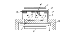
- the facing portion 6 of the limiting member 4 is sufficiently separated from the erosion region 5 so that the high-density plasma generated immediately above the erosion region 5 does not interfere, or the facing portion 6 does not exist on the limiting member 4. Therefore, the high-density plasma and the limiting member do not interfere with each other, so that the absorption of electrons by the limiting member is suppressed, and the limiting member can control the flight direction of the plasma particles while forming a thin film having a lower resistance film quality. The film becomes possible.
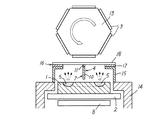
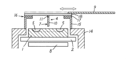
- a cathode 2 and an anode are provided in a vacuum chamber 12 so as to face each other.
- the substrate 3 to be deposited is disposed in the part, and an ionized Ar is applied by applying a DC high voltage between the substrate 3 and the cathode 2 while introducing an inert gas such as Ar into the vacuum chamber 12.
- an inert gas such as Ar
- a magnetron sputtering method is used in which a magnet 8 is arranged on the back surface of the cathode 2 and sputtering is performed by increasing the electron density in the vicinity of the cathode 2 by a generated magnetic field.
- This sputtering apparatus is used, for example, for manufacturing an electrode film of an LED lighting apparatus.
- this embodiment is an example of an inline sputtering apparatus in which the substrate 3 is sequentially transported by an inline transport mechanism as illustrated in FIG. 1, but the substrate 3 is rotated as in another example illustrated in FIG.
- the present invention can be similarly applied to a carousel sputtering apparatus that sequentially faces the target while being held by the drum 13.
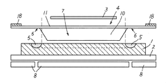
- a limiting member 4 for limiting the flying direction of the sputtered particles is provided between the cathode 2 and the substrate 3 (position where the substrate 3 is disposed).
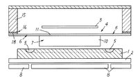
- the limiting member 4 is disposed so as to straddle the erosion region 5 formed in the target 1, and the distance ⁇ from the cathode 2 (target 1) of the facing portion 6 facing the erosion region 5 of the limiting member 4 is determined by the limiting member 4.
- the non-facing portion 7 that does not face the erosion region 5 located between the facing portions 6 is set to be larger than the distance ⁇ from the cathode 2 (target 1).
- does not face the erosion region 5 means that the erosion region 5 is far from the inner edge of the erosion region 5 to the extent that it does not interfere with the high-density plasma generated in the vicinity of the erosion region 5.
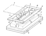
- the limiting member 4 of the present embodiment includes a rod body 11 laid between short-direction members 18 (described later), and the same width as the rod body 11 suspended from the rod body 11 and substantially perpendicular to the target 1. And a vertical plate portion 10 provided.
- the vertical plate portion 10 constitutes a non-facing portion 7 that does not face the erosion region 5, and the portion of the rod 11 facing the erosion region 5 constitutes the facing portion 6.
- the limiting member 4 of the present embodiment connects the limiting member support portion 15 erected on the base portion 14 provided on the bottom surface of the vacuum chamber 12, the limiting member support portion 15, the facing portion 6 and the non-facing portion 7. It is held by the connecting member 16.
- the connecting member 16 includes a longitudinal plate portion 17 disposed substantially parallel to the target surface along the longitudinal direction of the target 1 provided so as to surround the outer periphery of the left and right erosion regions 5 in plan view, and the short side of the target 1. It is comprised by the short direction member 18 arrange
- the longitudinal direction plate portion 17 is supported by the restricting member support portion 15, and the end portions of the rods 11 are fixed to the lower surface side of the short direction member 18, respectively. Note that the sputtered particles flying outside the left and right erosion regions 5 are restricted by the connecting member 16 (and the restricting member support portion 15).
- the restricting member 4 (the connecting member 16) is supported from below by the restricting member supporting portion 15, but the restricting member supporting portion 15 is vacuumed as in the second example shown in FIG. It is good also as a structure fixed to the top
- FIG. 1
- the limiting member 4 is configured to be disposed within a range of 20% or less of the maximum value of the horizontal magnetic field strength generated near the target surface by the magnet 8. is doing. That is, the facing portion 6 and the non-facing portion 7 are not arranged in a region exceeding 20% of the maximum horizontal magnetic field intensity generated in the vicinity of the target surface. If the limiting member 4 is in an area of 20% or less of the maximum value of the horizontal magnetic field strength, it is possible to limit the deposition angle of sputtered particles without hindering the movement of electrons in the high-density plasma area.
- the lower end of the non-facing portion 7 of the limiting member 4 is provided so as to be as close as possible to the target 1 within a range of 20% or less of the maximum value of the horizontal magnetic field strength.
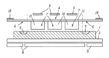
- the erosion region 5 is an annular portion that is more strongly sputtered than other portions by focusing the plasma at a high density by the magnetic field of the magnet 8 disposed on the back side of the cathode 2 (target 1). Then, it is the track shape comprised by the two linear parts 5a extended mutually substantially parallel, and the circular arc-shaped part 5b which each connects the both ends of this linear part 5a.
- the limiting member 4 of this embodiment is arranged so as to divide the annular erosion region 5 into a plurality when viewed from the substrate 3 side, and the flying direction of sputtered particles generated from the erosion region 5 divided into a plurality by the limiting member 4. It is comprised so that each may be restrict
- the non-facing portion 7 made of the vertical plate portion 10 is arranged in parallel to the linear portion 5a inside the erosion region 5, and the facing portion 6 of the rod 11 faces the arc-shaped portion 5b. Is arranged.
- the non-facing portion 7 of the limiting member 4 may be provided with a plate portion 19 substantially parallel to the target surface so as not to cover the erosion region 5, or illustrated in FIG. 8.
- the non-facing portion 7 is composed of a rectangular parallelepiped portion 20 whose width is less than the interval between the linear portions 5a, and flies in the direction of the restricting member 4 from the left and right erosion regions 5. It is good also as a structure which further restrict
- the film-forming shutter 9 that shields the sputtered particles on the substrate 3 may be provided on the limiting member 4 so that the film-forming shutter 9 moves relative to the cathode 2.
- a film forming shutter 9 is slidably provided above (or below) the restricting member 4 as shown in another example 5 shown in FIG. 9, and the film forming shutter 9 faces the target 1 when the film is not formed. 4 and the opening surrounded by the connecting member 16 may be closed. Further, the film forming shutter 9 is integrally provided adjacent to the restricting member 4 so that the restricting member 4 and the film forming shutter 9 are juxtaposed, and the restricting member 4 and the film forming shutter 9 are relative to the cathode 2.
- the target 1 and the limiting member 4 may be opposed to each other during film formation, and the target 1 and the film formation shutter 9 may be opposed to each other during film formation.
- the connecting portion between the non-facing portion 7 and the facing portion 6 is such that the bottom edge shape of both ends of the vertical plate portion 10 is gradually separated from the erosion region 5 toward the outer side, and the end portion of the vertical plate portion 10 faces. You may comprise so that the non-facing part 7 and the facing part 6 may be connected smoothly so that it may become the part 6.
- FIG. FIG. 10 shows another example 6 in which the lower edge shape of both ends of the vertical plate portion 10 is linear
- FIG. 11 shows another example 7 in which the shape is curved (R shape). In this case, the movement of the sputtered particles between the erosion regions 5 divided by the restricting member 4 can be more effectively restricted.
- the restricting member holding portion is, for example, a rod-like or string-like member that is thin enough not to restrict the flying of the sputtered particles, and has one end fixed to the short direction member 18 and the other end fixed to the non-facing portion 7. The facing part 7 is held.
- the present invention is not limited to the present embodiment, and the specific configuration of each component can be designed as appropriate.
Landscapes
- Chemical & Material Sciences (AREA)
- Chemical Kinetics & Catalysis (AREA)
- Engineering & Computer Science (AREA)
- Materials Engineering (AREA)
- Mechanical Engineering (AREA)
- Metallurgy (AREA)
- Organic Chemistry (AREA)
- Physical Vapour Deposition (AREA)
- Electrodes Of Semiconductors (AREA)
Abstract
Le but de la présente invention est de fournir un dispositif de pulvérisation qui peut réaliser une qualité de film de résistance inférieure par réduction de l'interférence entre un plasma haute densité et un élément de restriction. L'invention concerne un dispositif de pulvérisation comprenant : une cathode (2) sur laquelle une cible (1) est disposée ; un substrat (3) qui est disposé au niveau d'une position faisant face à la cible (1) ; et un élément de restriction (4) qui restreint la direction de vol des particules pulvérisées. Le dispositif de pulvérisation effectue un dépôt de film par dépôt de particules pulvérisées sur le substrat (3). Le dispositif de pulvérisation possède : une configuration dans laquelle l'élément de restriction (4) est disposé de façon à chevaucher des régions d'érosion (5) formées dans la cible (1), et dans laquelle une distance α, à partir de la cathode (2), de parties en vis-à-vis (6) de l'élément de restriction (4) qui font face aux régions d'érosion (5) est réglée pour être plus grande qu'une distance β, à partir de la cathode (2), d'une partie non en vis-à-vis (7) de l'élément de restriction (4) qui est située entre les parties en vis-à-vis (6) et ne fait pas face aux régions d'érosion (5) ; ou possède une configuration dans laquelle une partie de maintien d'élément de restriction qui maintient un élément de restriction (4) se composant de la partie non en vis-à-vis (7) est disposée de façon à chevaucher les régions d'érosion (5).
Applications Claiming Priority (2)
| Application Number | Priority Date | Filing Date | Title |
|---|---|---|---|
| JP2016-251502 | 2016-12-26 | ||
| JP2016251502A JP6948126B2 (ja) | 2016-12-26 | 2016-12-26 | スパッタ装置及び電極膜の製造方法 |
Publications (1)
| Publication Number | Publication Date |
|---|---|
| WO2018123776A1 true WO2018123776A1 (fr) | 2018-07-05 |
Family
ID=62707678
Family Applications (1)
| Application Number | Title | Priority Date | Filing Date |
|---|---|---|---|
| PCT/JP2017/045763 Ceased WO2018123776A1 (fr) | 2016-12-26 | 2017-12-20 | Dispositif de pulvérisation et procédé de production de film d'électrode |
Country Status (3)
| Country | Link |
|---|---|
| JP (1) | JP6948126B2 (fr) |
| TW (1) | TW201835364A (fr) |
| WO (1) | WO2018123776A1 (fr) |
Citations (3)
| Publication number | Priority date | Publication date | Assignee | Title |
|---|---|---|---|---|
| JPH0681146A (ja) * | 1992-09-01 | 1994-03-22 | Nec Corp | マグネトロン型スパッタ装置 |
| JPH08264451A (ja) * | 1994-12-16 | 1996-10-11 | Applied Materials Inc | 円筒状のスパッタリングシールド |
| JP2010031371A (ja) * | 2008-07-23 | 2010-02-12 | Seagate Technology Llc | スパッタリング装置、およびスパッタリング装置を介してターゲットから基板上へ材料をスパッタリングする方法 |
-
2016
- 2016-12-26 JP JP2016251502A patent/JP6948126B2/ja active Active
-
2017
- 2017-12-18 TW TW106144358A patent/TW201835364A/zh unknown
- 2017-12-20 WO PCT/JP2017/045763 patent/WO2018123776A1/fr not_active Ceased
Patent Citations (3)
| Publication number | Priority date | Publication date | Assignee | Title |
|---|---|---|---|---|
| JPH0681146A (ja) * | 1992-09-01 | 1994-03-22 | Nec Corp | マグネトロン型スパッタ装置 |
| JPH08264451A (ja) * | 1994-12-16 | 1996-10-11 | Applied Materials Inc | 円筒状のスパッタリングシールド |
| JP2010031371A (ja) * | 2008-07-23 | 2010-02-12 | Seagate Technology Llc | スパッタリング装置、およびスパッタリング装置を介してターゲットから基板上へ材料をスパッタリングする方法 |
Also Published As
| Publication number | Publication date |
|---|---|
| JP2018104758A (ja) | 2018-07-05 |
| TW201835364A (zh) | 2018-10-01 |
| JP6948126B2 (ja) | 2021-10-13 |
Similar Documents
| Publication | Publication Date | Title |
|---|---|---|
| KR20130035924A (ko) | 마그네트론 스퍼터 장치 및 방법 | |
| KR101430809B1 (ko) | 진공 성막 장치 | |
| WO2013011657A1 (fr) | Appareil de production d'un faisceau d'ions et appareil de traitement au plasma à faisceau d'ions | |
| CN105887026B (zh) | 物理气相沉积系统与应用其的物理气相沉积方法 | |
| KR20200137005A (ko) | 스퍼터링 캐소드, 스퍼터링 캐소드 집합체 및 스퍼터링 장치 | |
| JP6216177B2 (ja) | 電子ビーム蒸着装置 | |
| US9624570B2 (en) | Compact, filtered ion source | |
| KR20250076501A (ko) | 스퍼터링 장치 | |
| WO2018123776A1 (fr) | Dispositif de pulvérisation et procédé de production de film d'électrode | |
| WO2022019130A1 (fr) | Canon ionique et équipement de traitement sous vide | |
| JP6985570B1 (ja) | イオンガン及び真空処理装置 | |
| JP6088083B1 (ja) | 処理装置及びコリメータ | |
| TWI762872B (zh) | 濺射裝置 | |
| JP5421438B1 (ja) | プラズマ処理装置 | |
| US20080121515A1 (en) | Magnetron sputtering utilizing halbach magnet arrays | |
| JP2789251B2 (ja) | ダイポールリング型磁気回路を用いたスパッタ装置 | |
| TWI627297B (zh) | 用以濺鍍材料塗層於基板上之裝置及沉積系統 | |
| KR101817220B1 (ko) | 경사진 다중 루프 이온 소스, 이를 갖는 이온빔 처리 장치 및 이온빔 스퍼터링 장치 | |
| JP7320828B2 (ja) | スパッタリングカソード、スパッタリング装置、及び成膜体の製造方法 | |
| JP2006257498A (ja) | スパッタ源、スパッタ装置 | |
| JPS62174376A (ja) | スパツタ装置 | |
| KR20150093140A (ko) | 경사진 단일 루프 이온 소스, 이를 이용한 이온빔 처리 장치 및 이온빔 스퍼터링 장치 | |
| WO2014137552A1 (fr) | Système de dépôt physique en phase vapeur | |
| JP2017088973A (ja) | プラズマスパッタ装置 |
Legal Events
| Date | Code | Title | Description |
|---|---|---|---|
| 121 | Ep: the epo has been informed by wipo that ep was designated in this application |
Ref document number: 17887487 Country of ref document: EP Kind code of ref document: A1 |
|
| NENP | Non-entry into the national phase |
Ref country code: DE |
|
| 122 | Ep: pct application non-entry in european phase |
Ref document number: 17887487 Country of ref document: EP Kind code of ref document: A1 |