WO2018158902A1 - ポリフェーズフィルタ - Google Patents
ポリフェーズフィルタ Download PDFInfo
- Publication number
- WO2018158902A1 WO2018158902A1 PCT/JP2017/008239 JP2017008239W WO2018158902A1 WO 2018158902 A1 WO2018158902 A1 WO 2018158902A1 JP 2017008239 W JP2017008239 W JP 2017008239W WO 2018158902 A1 WO2018158902 A1 WO 2018158902A1
- Authority
- WO
- WIPO (PCT)
- Prior art keywords
- transistor
- terminal
- signal
- input
- output terminal
- Prior art date
- Legal status (The legal status is an assumption and is not a legal conclusion. Google has not performed a legal analysis and makes no representation as to the accuracy of the status listed.)
- Ceased
Links
Images




Classifications
-
- H—ELECTRICITY
- H03—ELECTRONIC CIRCUITRY
- H03H—IMPEDANCE NETWORKS, e.g. RESONANT CIRCUITS; RESONATORS
- H03H11/00—Networks using active elements
- H03H11/02—Multiple-port networks
- H03H11/04—Frequency selective two-port networks
-
- H—ELECTRICITY
- H03—ELECTRONIC CIRCUITRY
- H03H—IMPEDANCE NETWORKS, e.g. RESONANT CIRCUITS; RESONATORS
- H03H11/00—Networks using active elements
- H03H11/02—Multiple-port networks
- H03H11/04—Frequency selective two-port networks
- H03H11/0422—Frequency selective two-port networks using transconductance amplifiers, e.g. gmC filters
-
- H—ELECTRICITY
- H03—ELECTRONIC CIRCUITRY
- H03H—IMPEDANCE NETWORKS, e.g. RESONANT CIRCUITS; RESONATORS
- H03H11/00—Networks using active elements
- H03H11/02—Multiple-port networks
- H03H11/16—Networks for phase shifting
- H03H11/20—Two-port phase shifters providing an adjustable phase shift
-
- H—ELECTRICITY
- H03—ELECTRONIC CIRCUITRY
- H03H—IMPEDANCE NETWORKS, e.g. RESONANT CIRCUITS; RESONATORS
- H03H11/00—Networks using active elements
- H03H11/02—Multiple-port networks
- H03H11/16—Networks for phase shifting
- H03H11/22—Networks for phase shifting providing two or more phase shifted output signals, e.g. n-phase output
Definitions
- the present invention relates to a polyphase filter having a transistor.
- a semiconductor integrated circuit that processes a high-frequency received signal may be used.
- a semiconductor integrated circuit constituting a super heterodyne receiver for radar it is possible to suppress an image interference wave accompanying frequency conversion of a received signal in addition to a filter capable of limiting the band of the received signal.
- a polyphase filter or the like may be used.
- Patent Document 1 below discloses a polyphase filter including a plurality of resistors and a plurality of capacitors.
- the polyphase filter is a filter that is originally used for generating a signal having a phase difference of 90 degrees, but is also a filter capable of suppressing an image interference wave.
- the frequency at which the image interference wave can be suppressed changes according to the resistance value of the resistor and the capacitance value of the capacitor.
- the center frequency Fc of the frequency capable of suppressing the image interference wave is expressed by the following expression (1).
- R is the resistance value of the resistor
- C is the capacitance value of the capacitor.
- the conventional polyphase filter is configured as described above, by controlling the resistance value R of the provided resistor, it is possible to vary the frequency at which the image interference wave can be suppressed.
- the polyphase filter is configured using a resistor, which is a passive element, there is a problem in that a passage loss occurs when suppressing an image interference wave.
- the present invention has been made to solve the above-described problems, and an object thereof is to obtain a polyphase filter that can suppress the occurrence of a passage loss.
- the polyphase filter according to the present invention includes a first transistor that amplifies the first I signal input from the first input terminal, and a first transistor that amplifies the first Q signal input from the second input terminal. And a second transistor that amplifies the second I signal when a second I signal that constitutes a differential signal with the first I signal is input from the third input terminal; When the second Q signal constituting the differential signal with the first Q signal is input from the fourth input terminal, the fourth transistor for amplifying the second Q signal, and the first transistor A first capacitor connected between the output terminal and the second input terminal; a second capacitor connected between the output terminal of the second transistor and the third input terminal; Connected between the output terminal of the third transistor and the fourth input terminal. A third capacitor being, is obtained by so and a fourth capacitor connected between the output terminal and the first input terminal of the fourth transistor.
- the first transistor that amplifies the first I signal input from the first input terminal and the second transistor that amplifies the first Q signal input from the second input terminal A third transistor for amplifying the second I signal when the second I signal constituting the differential signal with the first I signal is input from the third input terminal; When the second Q signal that constitutes the Q signal and the differential signal is input from the fourth input terminal, the fourth transistor that amplifies the second Q signal is provided. There is an effect of suppressing the generation of loss.
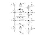
- FIG. 1 is a circuit diagram showing a polyphase filter according to Embodiment 1 of the present invention.
- a first input terminal 1a is a terminal to which a first I signal VIP is input.
- the second input terminal 1b is a terminal to which the first Q signal V QP is input.
- the third input terminal 1c is a terminal to which the first I signal VIP and the second I signal VIN constituting a differential signal are input.
- V IP + V IN 0.
- the fourth input terminal 1d is a terminal to which the first Q signal V QP and the second Q signal V QN constituting a differential signal are input.
- V QP + V QN 0.
- the first transistor 2a has a transconductance g m, a bipolar transistor having an emitter terminal is grounded.
- the first transistor 2a has a base terminal connected to the first input terminal 1a, a collector terminal (output terminal of the first transistor 2a) connected to the first output terminal 4a, and a first input terminal. amplifying the first I signal V IP input from 1a, and outputs a first I signal V IP after amplification to the first output terminal 4a.
- the second transistor 2b has a transconductance g m, a bipolar transistor having an emitter terminal is grounded.
- the second transistor 2b has a base terminal connected to the second input terminal 1b, a collector terminal (output terminal of the second transistor 2b) connected to the second output terminal 4b, and a second input terminal.
- the first Q signal V QP input from 1b is amplified, and the amplified first Q signal V QP is output to the second output terminal 4b.
- the third transistor 2c has a transconductance g m, a bipolar transistor having an emitter terminal is grounded.
- the third transistor 2c has a base terminal connected to the third input terminal 1c, a collector terminal (output terminal of the third transistor 2c) connected to the third output terminal 4c, and a third input terminal.
- the second I signal VIN input from 1c is amplified, and the amplified second I signal VIN is output to the third output terminal 4c.
- Fourth transistor 2d has a transconductance g m, a bipolar transistor having an emitter terminal is grounded.
- the fourth transistor 2d has a base terminal connected to the fourth input terminal 1d, a collector terminal (output terminal of the fourth transistor 2d) connected to the fourth output terminal 4d, and a fourth input terminal.
- the second Q signal V QN input from 1d is amplified, and the amplified second Q signal V QN is output to the fourth output terminal 4d.
- the first capacitor 3a is connected to the collector terminal of the first transistor 2a, and the other end is connected to the second input terminal 1b.
- the second capacitor 3b has one end connected to the collector terminal of the second transistor 2b and the other end connected to the third input terminal 1c.
- the third capacitor 3c has one end connected to the collector terminal of the third transistor 2c and the other end connected to the fourth input terminal 1d.
- the fourth capacitor 3d has one end connected to the collector terminal of the fourth transistor 2d and the other end connected to the first input terminal 1a.
- the first output terminal 4a is connected to the collector terminal of the first transistor 2a, and is a terminal for outputting the first I signal VO_IP amplified by the first transistor 2a.
- the second output terminal 4b is connected to the collector terminal of the second transistor 2b, and is a terminal for outputting the first Q signal VO_QP amplified by the second transistor 2b.
- the third output terminal 4c is connected to the collector terminal of the third transistor 2c, and is a terminal for outputting the second I signal V O_IN amplified by the third transistor 2c.
- the fourth output terminal 4d is connected to the collector terminal of the fourth transistor 2d, and is a terminal for outputting the second Q signal VO_QN amplified by the fourth transistor 2d.
- FIG. 2 is a circuit diagram showing another polyphase filter according to Embodiment 1 of the present invention.
- the polyphase filter of FIG. 2 is different from the polyphase filter of FIG. 1 in that the collector terminals (output terminals) of the first to fourth transistors are connected to the power supply Vcc through a load.
- the load 5a is a resistor having an impedance Z, one end is connected to the collector terminal of the first transistor 2a, and the other end is connected to the power supply Vcc.
- the load 5b is a resistor having an impedance Z, one end is connected to the collector terminal of the second transistor 2b, and the other end is connected to the power source Vcc.
- the load 5c is a resistor having an impedance Z, one end is connected to the collector terminal of the third transistor 2c, and the other end is connected to the power source Vcc.
- the load 5d is a resistor having an impedance Z, one end is connected to the collector terminal of the fourth transistor 2d, and the other end is connected to the power supply Vcc.
- a load circuit such as a transimpedance amplifier is connected to each of the first output terminal 4a, the second output terminal 4b, the third output terminal 4c, and the fourth output terminal 4d. When such a load circuit is connected, it is not necessary to connect the loads 5a to 5d as shown in FIG.
- FIG. 3 is a circuit diagram showing a conventional polyphase filter having a resistor.
- the resistor 6a is connected between the first input terminal 1a and the first output terminal 4a.
- the resistor 6b is connected between the second input terminal 1b and the second output terminal 4b.
- the resistor 6c is connected between the third input terminal 1c and the third output terminal 4c.
- the resistor 6d is connected between the fourth input terminal 1d and the fourth output terminal 4d.
- ⁇ V IOUT V O_IP ⁇ V O_IN .
- the current I a flowing through the resistor 6a is expressed by the following equation (2)
- the current I b flowing through the first capacitor 3a is expressed by the following equation (3).
- the first I signal VO_IP output from the first output terminal 4a is expressed by the following equation (4).
- R is the resistance value of the resistor 6a
- C is the capacitance value of the first capacitor 3a
- Z is the impedance of the load 5a.
- a first I signal V O_IP output from the first output terminal 4a is The following equation (5) is obtained.
- the first I signal V O_IP has been described, but the second I signal V O_IN can be obtained in the same manner.
- the second I signal V O_IN is expressed as the following equation (6).
- the differential signal ⁇ V IOUT related to the I signal is obtained.
- the differential signal ⁇ V IOUT is expressed as the following equation (7).
- ⁇ V QOUT V O_QP ⁇ V O_QN .
- the current If flowing through the resistor 6b is expressed by the following equation (8)
- the current Ie flowing through the second capacitor 3b is expressed by the following equation (9). Therefore, the first Q signal VO_QP output from the second output terminal 4b is expressed by the following equation (10).
- R is the resistance value of the resistor 6b
- C is the capacitance value of the second capacitor 3b
- Z is the impedance of the load 5b.
- the first Q signal V O_QP output from the second output terminal 4b is The following equation (11) is obtained.
- the first Q signal V O_QP has been described here, the second Q signal V O_QN can be obtained in the same manner.
- the second Q signal V O_QN is expressed as the following Expression (12).
- the differential signal ⁇ V QOUT related to the Q signal is obtained.
- the differential signal ⁇ V QOUT is expressed as the following equation (13).
- the input of the polyphase filter is short-circuited by IQ as shown in the following equation (14).
- ⁇ V IOUT V O_IP ⁇ V O_IN .
- the current I a flowing through the first transistor 2a is expressed by the following equation (17)
- the current I b flowing through the first capacitor 3a is expressed by the following equation (18). Therefore, the first I signal V O_IP output from the first output terminal 4a is expressed by the following equation (18).
- g m is the transconductance of the first transistor 2a.
- a first I signal V O_IP output from the first output terminal 4a is The following equation (20) is obtained.
- the first I signal V O_IP has been described, but the second I signal V O_IN can be obtained in the same manner.
- the second I signal V O_IN is expressed as the following Expression (21).
- the differential signal ⁇ V IOUT related to the I signal is obtained.
- the differential signal ⁇ V IOUT is expressed as the following equation (22).
- ⁇ V QOUT V O_QP ⁇ V O_QN .
- the current If flowing through the second transistor 2b is expressed by the following equation (23), and the current Ie flowing through the second capacitor 3b is expressed by the following equation (24). Therefore, the first Q signal VO_QP output from the second output terminal 4b is expressed by the following equation (25).
- the first Q signal V O_QP output from the second output terminal 4b is The following equation (26) is obtained.
- the first Q signal V O_QP has been described here, the second Q signal V O_QN can be obtained in the same manner.
- the second Q signal V O_QN is expressed as in the following Expression (27).
- the differential signal ⁇ V QOUT related to the Q signal is obtained.
- the differential signal ⁇ V QOUT is expressed as the following equation (28).
- the resistors 6a to 6d of the polyphase filter in FIG. 3 are replaced with the first transistor 2a, the second transistor 2b, the third transistor 2c, and the fourth transistor 2d. Is different. Therefore, also in the polyphase filter of the first embodiment, the amplitude of the IQ signal is always constant and the phase of the IQ signal is 90 degrees different at the angular frequency ⁇ , as in the polyphase filter of FIG. Therefore, the polyphase filter of the first embodiment can realize the same IQ characteristics as the polyphase filter of FIG. However, poly-phase filter of the first embodiment is different from the polyphase filter of Fig. 3, since it is configured using a transistor having a transconductance g m, it is possible to have a gain.
- the gain that the polyphase filter of the first embodiment can have is determined by the magnitude relationship between transconductance g m and ⁇ C, as shown in Table 2 below.
- ⁇ is an angular frequency
- C is a capacitance value of the first capacitor 3a, the second capacitor 3b, the third capacitor 3c, and the fourth capacitor 3d.
- the polyphase filter of the first embodiment can have a gain of 1 or more regardless of the magnitude relationship between transconductance g m and ⁇ C.
- the second transistor 2b that amplifies the input first Q signal V QP and the second I signal VIN that forms a differential signal with the first I signal V IP are the third input terminal 1c.
- the fourth transistor 2d for amplifying the second Q signal V QN is provided, so that it is possible to suppress the occurrence of passage loss.
- the collector terminals of the first transistor 2a, the second transistor 2b, the third transistor 2c, and the fourth transistor 2d are respectively connected via the loads 5a, 5b, 5c, and 5d.
- an NPN bipolar transistor can be used as the first transistor 2a, the second transistor 2b, the third transistor 2c, and the fourth transistor 2d.
- the first transistor 2a, the second transistor 2b, the third transistor 2c and the fourth transistor 2d is, an example is a bipolar transistor having a transconductance g m As long as it is, it is not limited to a bipolar transistor. Therefore, the first transistor 2a, the second transistor 2b, the third transistor 2c, and the fourth transistor 2d may be, for example, a field effect transistor or a MOS such as a CMOS (Complementary Metal Oxide Semiconductor). It may be a transistor.
- the gate terminal of the field effect transistor corresponds to the base terminal of the bipolar transistor.
- the drain terminal of the field effect transistor corresponds to the collector terminal of the bipolar transistor, and the source terminal of the field effect transistor corresponds to the emitter terminal of the bipolar transistor.
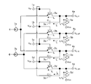
- Embodiment 2 FIG. In the first embodiment, an example is shown in which the emitter terminals of the first transistor 2a, the second transistor 2b, the third transistor 2c, and the fourth transistor 2d are grounded. In the second embodiment, the emitter terminal of the first transistor 2a and the emitter terminal of the third transistor 2c are connected to the ground through the first current source 7a, and the emitter terminal of the second transistor 2b and the fourth transistor An example in which the emitter terminal of the transistor 2d is connected to the ground via the second current source 7b will be described.
- FIG. 4 is a circuit diagram showing a polyphase filter according to Embodiment 2 of the present invention.
- the first current source 7a has a positive side connected to the emitter terminal of the first transistor 2a and the third transistor 2c, and a negative side connected to the ground.
- the second current source 7b has a positive side connected to the emitter terminal of the second transistor 2b and the fourth transistor 2d, and a negative side connected to the ground.
- the collector terminals of the first transistor 2a, the second transistor 2b, the third transistor 2c, and the fourth transistor 2d are connected to the power source Vcc through loads 5a, 5b, 5c, and 5d, respectively.
- a load circuit such as a transimpedance amplifier is connected to each of the first output terminal 4a, the second output terminal 4b, the third output terminal 4c, and the fourth output terminal 4d, the load 5a ⁇ 5d need not be connected.
- the emitter terminal of the second transistor 2b and the emitter terminal of the fourth transistor 2d are by being connected to the ground via a second current source 7b, a current I f flowing through the second transistor 2b, and the current I h flowing in the fourth transistor 2d becomes a differential signal.
- the accuracy of suppressing the image interference wave by the polyphase filter can be improved as compared with the first embodiment.
- the emitter terminal of the first transistor 2a and the emitter terminal of the third transistor 2c are connected to the ground via the first current source 7a, and the emitter terminal and the second transistor 2b of the second transistor 2b are connected.
- the emitter terminal of the fourth transistor 2d is connected to the ground via the second current source 7b.
- the first resistor 8a is connected in place of the first current source 7a
- the second resistor 8b is connected in place of the second current source 7b. An effect can be obtained.
- FIG. 5 is a circuit diagram showing another polyphase filter according to Embodiment 2 of the present invention.
- the first transistor 2a, the second transistor 2b, the third transistor 2c, and the fourth transistor 2d are bipolar transistors.
- it may be a field effect transistor or a MOS transistor such as a CMOS.
- Embodiment 3 In the first embodiment, an example is shown in which the emitter terminals of the first transistor 2a, the second transistor 2b, the third transistor 2c, and the fourth transistor 2d are grounded. In the third embodiment, an example in which the base terminals of the first transistor 9a, the second transistor 9b, the third transistor 9c, and the fourth transistor 9d are grounded will be described.
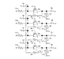
- FIG. 6 is a circuit diagram showing a polyphase filter according to Embodiment 3 of the present invention.
- the first transistor 9a has a transconductance g m, a bipolar transistor having a base terminal is grounded.
- the first transistor 9a has an emitter terminal connected to the first input terminal 1a, a collector terminal (output terminal of the first transistor 9a) connected to the first output terminal 4a, and a first input terminal. amplifying the first I signal V IP input from 1a, and outputs a first I signal V IP after amplification to the first output terminal 4a.
- the second transistor 9b has a transconductance g m, a bipolar transistor having a base terminal is grounded.
- the second transistor 9b has an emitter terminal connected to the second input terminal 1b, a collector terminal (output terminal of the second transistor 9b) connected to the second output terminal 4b, and a second input terminal.
- the first Q signal V QP input from 1b is amplified, and the amplified first Q signal V QP is output to the second output terminal 4b.
- the third transistor 9c has a transconductance g m, a bipolar transistor having a base terminal is grounded.
- the third transistor 9c has an emitter terminal connected to the third input terminal 1c, a collector terminal (an output terminal of the third transistor 9c) connected to the third output terminal 4c, and a third input terminal.
- the second I signal VIN input from 1c is amplified, and the amplified second I signal VIN is output to the third output terminal 4c.
- Fourth transistor 9d has a transconductance g m, a bipolar transistor having a base terminal is grounded.
- the fourth transistor 9d has an emitter terminal connected to the fourth input terminal 1d, a collector terminal (output terminal of the fourth transistor 9d) connected to the fourth output terminal 4d, and a fourth input terminal.
- the second Q signal V QN input from 1d is amplified, and the amplified second Q signal V QN is output to the fourth output terminal 4d.
- the first current source 10a has a positive side connected to the emitter terminal of the first transistor 9a and a negative side connected to the ground.
- the second current source 10b has a positive side connected to the emitter terminal of the second transistor 9b and a negative side connected to the ground.
- the third current source 10c has a positive side connected to the emitter terminal of the third transistor 9c and a negative side connected to the ground.
- the fourth current source 10d has a positive side connected to the emitter terminal of the fourth transistor 9d and a negative side connected to the ground.
- the collector terminals of the first transistor 9a, the second transistor 9b, the third transistor 9c, and the fourth transistor 9d are connected to the power source Vcc through loads 5a, 5b, 5c, and 5d, respectively.
- a load circuit such as a transimpedance amplifier is connected to each of the first output terminal 4a, the second output terminal 4b, the third output terminal 4c, and the fourth output terminal 4d, the load 5a ⁇ 5d need not be connected.
- the operation of the polyphase filter of the third embodiment is almost the same as the operation of the polyphase filter of the first embodiment.
- the base terminals of the first transistor 9a, the second transistor 9b, the third transistor 9c, and the fourth transistor 9d are grounded. Therefore, the input impedance viewed from the first input terminal 1a, the second input terminal 1b, the third input terminal 1c, and the fourth input terminal 1d is expressed as the first transistor 9a, the second transistor 9b, it can be 1 / g m of the impedance in the third transistor 9c and the fourth transistor 9d.
- the first transistor 9a and the second transistor 9b according to the output impedance viewed from the first output terminal 4a, the second output terminal 4b, the third output terminal 4c, and the fourth output terminal 4d.
- the transconductance g m of the third transistor 9c and the fourth transistor 9d it is possible to realize a wideband input matching. Further, unnecessary matching elements can be eliminated to achieve downsizing and wideband performance can be realized.
- the emitter terminal of the first transistor 9a is connected to the ground via the first current source 10a
- the emitter terminal of the second transistor 9b is connected to the ground via the second current source 10b. It is connected.
- the emitter terminal of the third transistor 9c is connected to the ground via the third current source 10c
- the emitter terminal of the fourth transistor 9d is connected to the ground via the fourth current source 10d.
- a first resistor 11a is connected instead of the first current source 10a
- a second resistor 11b is connected instead of the second current source 10b
- the third current source 10c instead, the third resistor 11c may be connected, and the fourth resistor 11d may be connected instead of the fourth current source 10d. In this case, the same effect can be obtained.
- FIG. 7 is a circuit diagram showing another polyphase filter according to Embodiment 3 of the present invention.
- the first transistor 9a, the second transistor 9b, the third transistor 9c, and the fourth transistor 9d are bipolar transistors.
- the first transistor 9a, The second transistor 9b, the third transistor 9c, and the fourth transistor 9d may be, for example, field effect transistors or MOS transistors such as CMOS.
- the present invention is suitable for a polyphase filter including a transistor.
Landscapes
- Networks Using Active Elements (AREA)
Abstract
第1の入力端子(1a)から入力される第1のI信号VIPを増幅する第1のトランジスタ(2a)と、第2の入力端子(1b)から入力される第1のQ信号VQPを増幅する第2のトランジスタ(2b)と、第1のI信号VIPと差動信号を構成している第2のI信号VINが第3の入力端子(1c)から入力されると、第2のI信号VINを増幅する第3のトランジスタ(2c)と、第1のQ信号VQPと差動信号を構成している第2のQ信号VQNが第4の入力端子(1d)から入力されると、第2のQ信号VQNを増幅する第4のトランジスタ(2d)とを備える。
Description
この発明は、トランジスタを備えているポリフェーズフィルタに関するものである。
無線通信機器においては、高周波の受信信号を処理する半導体集積回路が用いられることがある。
例えば、レーダ用のスーパーヘテロダイン受信機を構成する半導体集積回路においては、受信信号の帯域を制限することが可能なフィルタのほか、受信信号の周波数変換に伴うイメージ妨害波を抑圧することが可能なポリフェーズフィルタなどが用いられることがある。
以下の特許文献1には、複数の抵抗と、複数のコンデンサとを備えたポリフェーズフィルタが開示されている。
例えば、レーダ用のスーパーヘテロダイン受信機を構成する半導体集積回路においては、受信信号の帯域を制限することが可能なフィルタのほか、受信信号の周波数変換に伴うイメージ妨害波を抑圧することが可能なポリフェーズフィルタなどが用いられることがある。
以下の特許文献1には、複数の抵抗と、複数のコンデンサとを備えたポリフェーズフィルタが開示されている。
ポリフェーズフィルタは、本来、90度の位相差がある信号の生成等に用いられるフィルタであるが、イメージ妨害波を抑圧することが可能なフィルタでもある。
ポリフェーズフィルタは、備えている抵抗の抵抗値及びコンデンサの容量値に応じて、イメージ妨害波を抑圧することが可能な周波数が変化する。
イメージ妨害波を抑圧することが可能な周波数の中心周波数Fcは、以下の式(1)で表される。
 式(1)において、Rは抵抗の抵抗値、Cはコンデンサの容量値である。
ポリフェーズフィルタは、備えている抵抗の抵抗値及びコンデンサの容量値に応じて、イメージ妨害波を抑圧することが可能な周波数が変化する。
イメージ妨害波を抑圧することが可能な周波数の中心周波数Fcは、以下の式(1)で表される。
従来のポリフェーズフィルタは以上のように構成されているので、備えている抵抗の抵抗値Rを制御することで、イメージ妨害波を抑圧することが可能な周波数を可変することができる。しかし、ポリフェーズフィルタは、受動素子である抵抗を用いて構成されているため、イメージ妨害波を抑圧する際、通過ロスが発生してしまうという課題があった。
この発明は上記のような課題を解決するためになされたもので、通過ロスの発生を抑えることができるポリフェーズフィルタを得ることを目的とする。
この発明に係るポリフェーズフィルタは、第1の入力端子から入力される第1のI信号を増幅する第1のトランジスタと、第2の入力端子から入力される第1のQ信号を増幅する第2のトランジスタと、第1のI信号と差動信号を構成している第2のI信号が第3の入力端子から入力されると、第2のI信号を増幅する第3のトランジスタと、第1のQ信号と差動信号を構成している第2のQ信号が第4の入力端子から入力されると、第2のQ信号を増幅する第4のトランジスタと、第1のトランジスタの出力端子と第2の入力端子との間に接続されている第1のコンデンサと、第2のトランジスタの出力端子と第3の入力端子との間に接続されている第2のコンデンサと、第3のトランジスタの出力端子と第4の入力端子との間に接続されている第3のコンデンサと、第4のトランジスタの出力端子と第1の入力端子との間に接続されている第4のコンデンサとを備えるようにしたものである。
この発明によれば、第1の入力端子から入力される第1のI信号を増幅する第1のトランジスタと、第2の入力端子から入力される第1のQ信号を増幅する第2のトランジスタと、第1のI信号と差動信号を構成している第2のI信号が第3の入力端子から入力されると、第2のI信号を増幅する第3のトランジスタと、第1のQ信号と差動信号を構成している第2のQ信号が第4の入力端子から入力されると、第2のQ信号を増幅する第4のトランジスタとを備えるように構成したので、通過ロスの発生を抑えることができる効果がある。
以下、この発明をより詳細に説明するために、この発明を実施するための形態について、添付の図面に従って説明する。
実施の形態1.
図1はこの発明の実施の形態1によるポリフェーズフィルタを示す回路図である。
図1において、第1の入力端子1aは第1のI信号VIPが入力される端子である。
第2の入力端子1bは第1のQ信号VQPが入力される端子である。
第3の入力端子1cは第1のI信号VIPと差動信号を構成している第2のI信号VINが入力される端子である。理想的には、VIP+VIN=0である。
第4の入力端子1dは第1のQ信号VQPと差動信号を構成している第2のQ信号VQNが入力される端子である。理想的には、VQP+VQN=0である。
図1はこの発明の実施の形態1によるポリフェーズフィルタを示す回路図である。
図1において、第1の入力端子1aは第1のI信号VIPが入力される端子である。
第2の入力端子1bは第1のQ信号VQPが入力される端子である。
第3の入力端子1cは第1のI信号VIPと差動信号を構成している第2のI信号VINが入力される端子である。理想的には、VIP+VIN=0である。
第4の入力端子1dは第1のQ信号VQPと差動信号を構成している第2のQ信号VQNが入力される端子である。理想的には、VQP+VQN=0である。
第1のトランジスタ2aはトランスコンダクタンスgmを有し、エミッタ端子が接地されているバイポーラトランジスタである。
第1のトランジスタ2aは、ベース端子が第1の入力端子1aと接続され、コレクタ端子(第1のトランジスタ2aの出力端子)が第1の出力端子4aと接続されており、第1の入力端子1aから入力された第1のI信号VIPを増幅して、増幅後の第1のI信号VIPを第1の出力端子4aに出力する。
第2のトランジスタ2bはトランスコンダクタンスgmを有し、エミッタ端子が接地されているバイポーラトランジスタである。
第2のトランジスタ2bは、ベース端子が第2の入力端子1bと接続され、コレクタ端子(第2のトランジスタ2bの出力端子)が第2の出力端子4bと接続されており、第2の入力端子1bから入力された第1のQ信号VQPを増幅して、増幅後の第1のQ信号VQPを第2の出力端子4bに出力する。
第1のトランジスタ2aは、ベース端子が第1の入力端子1aと接続され、コレクタ端子(第1のトランジスタ2aの出力端子)が第1の出力端子4aと接続されており、第1の入力端子1aから入力された第1のI信号VIPを増幅して、増幅後の第1のI信号VIPを第1の出力端子4aに出力する。
第2のトランジスタ2bはトランスコンダクタンスgmを有し、エミッタ端子が接地されているバイポーラトランジスタである。
第2のトランジスタ2bは、ベース端子が第2の入力端子1bと接続され、コレクタ端子(第2のトランジスタ2bの出力端子)が第2の出力端子4bと接続されており、第2の入力端子1bから入力された第1のQ信号VQPを増幅して、増幅後の第1のQ信号VQPを第2の出力端子4bに出力する。
第3のトランジスタ2cはトランスコンダクタンスgmを有し、エミッタ端子が接地されているバイポーラトランジスタである。
第3のトランジスタ2cは、ベース端子が第3の入力端子1cと接続され、コレクタ端子(第3のトランジスタ2cの出力端子)が第3の出力端子4cと接続されており、第3の入力端子1cから入力された第2のI信号VINを増幅して、増幅後の第2のI信号VINを第3の出力端子4cに出力する。
第4のトランジスタ2dはトランスコンダクタンスgmを有し、エミッタ端子が接地されているバイポーラトランジスタである。
第4のトランジスタ2dは、ベース端子が第4の入力端子1dと接続され、コレクタ端子(第4のトランジスタ2dの出力端子)が第4の出力端子4dと接続されており、第4の入力端子1dから入力された第2のQ信号VQNを増幅して、増幅後の第2のQ信号VQNを第4の出力端子4dに出力する。
第3のトランジスタ2cは、ベース端子が第3の入力端子1cと接続され、コレクタ端子(第3のトランジスタ2cの出力端子)が第3の出力端子4cと接続されており、第3の入力端子1cから入力された第2のI信号VINを増幅して、増幅後の第2のI信号VINを第3の出力端子4cに出力する。
第4のトランジスタ2dはトランスコンダクタンスgmを有し、エミッタ端子が接地されているバイポーラトランジスタである。
第4のトランジスタ2dは、ベース端子が第4の入力端子1dと接続され、コレクタ端子(第4のトランジスタ2dの出力端子)が第4の出力端子4dと接続されており、第4の入力端子1dから入力された第2のQ信号VQNを増幅して、増幅後の第2のQ信号VQNを第4の出力端子4dに出力する。
第1のコンデンサ3aは一端が第1のトランジスタ2aのコレクタ端子と接続され、他端が第2の入力端子1bと接続されている。
第2のコンデンサ3bは一端が第2のトランジスタ2bのコレクタ端子と接続され、他端が第3の入力端子1cと接続されている。
第3のコンデンサ3cは一端が第3のトランジスタ2cのコレクタ端子と接続され、他端が第4の入力端子1dと接続されている。
第4のコンデンサ3dは一端が第4のトランジスタ2dのコレクタ端子と接続され、他端が第1の入力端子1aと接続されている。
第2のコンデンサ3bは一端が第2のトランジスタ2bのコレクタ端子と接続され、他端が第3の入力端子1cと接続されている。
第3のコンデンサ3cは一端が第3のトランジスタ2cのコレクタ端子と接続され、他端が第4の入力端子1dと接続されている。
第4のコンデンサ3dは一端が第4のトランジスタ2dのコレクタ端子と接続され、他端が第1の入力端子1aと接続されている。
第1の出力端子4aは第1のトランジスタ2aのコレクタ端子と接続されており、第1のトランジスタ2aにより増幅された第1のI信号VO_IPを出力する端子である。
第2の出力端子4bは第2のトランジスタ2bのコレクタ端子と接続されており、第2のトランジスタ2bにより増幅された第1のQ信号VO_QPを出力する端子である。
第3の出力端子4cは第3のトランジスタ2cのコレクタ端子と接続されており、第3のトランジスタ2cにより増幅された第2のI信号VO_INを出力する端子である。
第4の出力端子4dは第4のトランジスタ2dのコレクタ端子と接続されており、第4のトランジスタ2dにより増幅された第2のQ信号VO_QNを出力する端子である。
第2の出力端子4bは第2のトランジスタ2bのコレクタ端子と接続されており、第2のトランジスタ2bにより増幅された第1のQ信号VO_QPを出力する端子である。
第3の出力端子4cは第3のトランジスタ2cのコレクタ端子と接続されており、第3のトランジスタ2cにより増幅された第2のI信号VO_INを出力する端子である。
第4の出力端子4dは第4のトランジスタ2dのコレクタ端子と接続されており、第4のトランジスタ2dにより増幅された第2のQ信号VO_QNを出力する端子である。
図2はこの発明の実施の形態1による他のポリフェーズフィルタを示す回路図である。
図2のポリフェーズフィルタは、第1から第4のトランジスタのコレクタ端子(出力端子)のそれぞれが負荷を介して電源Vccと接続されている点で、図1のポリフェーズフィルタと相違している。
負荷5aはインピーダンスがZの抵抗であり、一端が第1のトランジスタ2aのコレクタ端子と接続され、他端が電源Vccと接続されている。
負荷5bはインピーダンスがZの抵抗であり、一端が第2のトランジスタ2bのコレクタ端子と接続され、他端が電源Vccと接続されている。
負荷5cはインピーダンスがZの抵抗であり、一端が第3のトランジスタ2cのコレクタ端子と接続され、他端が電源Vccと接続されている。
負荷5dはインピーダンスがZの抵抗であり、一端が第4のトランジスタ2dのコレクタ端子と接続され、他端が電源Vccと接続されている。
図1のポリフェーズフィルタでは、第1の出力端子4a、第2の出力端子4b、第3の出力端子4c及び第4の出力端子4dのそれぞれに、トランスインピーダンスアンプなどの負荷回路が接続されていることを想定しており、このような負荷回路が接続されている場合、図2のように負荷5a~5dが接続されている必要はない。
図2のポリフェーズフィルタは、第1から第4のトランジスタのコレクタ端子(出力端子)のそれぞれが負荷を介して電源Vccと接続されている点で、図1のポリフェーズフィルタと相違している。
負荷5aはインピーダンスがZの抵抗であり、一端が第1のトランジスタ2aのコレクタ端子と接続され、他端が電源Vccと接続されている。
負荷5bはインピーダンスがZの抵抗であり、一端が第2のトランジスタ2bのコレクタ端子と接続され、他端が電源Vccと接続されている。
負荷5cはインピーダンスがZの抵抗であり、一端が第3のトランジスタ2cのコレクタ端子と接続され、他端が電源Vccと接続されている。
負荷5dはインピーダンスがZの抵抗であり、一端が第4のトランジスタ2dのコレクタ端子と接続され、他端が電源Vccと接続されている。
図1のポリフェーズフィルタでは、第1の出力端子4a、第2の出力端子4b、第3の出力端子4c及び第4の出力端子4dのそれぞれに、トランスインピーダンスアンプなどの負荷回路が接続されていることを想定しており、このような負荷回路が接続されている場合、図2のように負荷5a~5dが接続されている必要はない。
図3は抵抗を備えている従来のポリフェーズフィルタを示す回路図であり、図3において、図1及び図2と同一符号は同一または相当部分を示している。
抵抗6aは第1の入力端子1aと第1の出力端子4aとの間に接続されている。
抵抗6bは第2の入力端子1bと第2の出力端子4bとの間に接続されている。
抵抗6cは第3の入力端子1cと第3の出力端子4cとの間に接続されている。
抵抗6dは第4の入力端子1dと第4の出力端子4dとの間に接続されている。
抵抗6aは第1の入力端子1aと第1の出力端子4aとの間に接続されている。
抵抗6bは第2の入力端子1bと第2の出力端子4bとの間に接続されている。
抵抗6cは第3の入力端子1cと第3の出力端子4cとの間に接続されている。
抵抗6dは第4の入力端子1dと第4の出力端子4dとの間に接続されている。
次に動作について説明する。
この実施の形態1のポリフェーズフィルタとの比較のために、図3に示す従来のポリフェーズフィルタを解析する。
まず、従来のポリフェーズフィルタから出力されるI信号に係る差動信号ΔVIOUTについて説明する。ΔVIOUT=VO_IP-VO_INである。
例えば、抵抗6aを流れる電流Iaは、以下の式(2)で表され、第1のコンデンサ3aを流れる電流Ibは、以下の式(3)で表される。
このため、第1の出力端子4aから出力される第1のI信号VO_IPは、以下の式(4)で表される。


 式(2)~(4)において、Rは抵抗6aの抵抗値、Cは第1のコンデンサ3aの容量値、Zは負荷5aのインピーダンスである。
この実施の形態1のポリフェーズフィルタとの比較のために、図3に示す従来のポリフェーズフィルタを解析する。
まず、従来のポリフェーズフィルタから出力されるI信号に係る差動信号ΔVIOUTについて説明する。ΔVIOUT=VO_IP-VO_INである。
例えば、抵抗6aを流れる電流Iaは、以下の式(2)で表され、第1のコンデンサ3aを流れる電流Ibは、以下の式(3)で表される。
このため、第1の出力端子4aから出力される第1のI信号VO_IPは、以下の式(4)で表される。
式(2)で表される電流Ia及び式(3)で表される電流Ibを式(4)に代入すると、第1の出力端子4aから出力される第1のI信号VO_IPは、以下の式(5)のようになる。
 ここでは、第1のI信号VO_IPについて説明しているが、第2のI信号VO_INについても同様に得ることができる。
第2のI信号VO_INは、以下の式(6)のように表される。

第2のI信号VO_INは、以下の式(6)のように表される。
式(5)及び式(6)より、I信号に係る差動信号ΔVIOUTが得られる。差動信号ΔVIOUTは、以下の式(7)のように表される。

次に、従来のポリフェーズフィルタから出力されるQ信号に係る差動信号ΔVQOUTについて説明する。ΔVQOUT=VO_QP-VO_QNである。
例えば、抵抗6bを流れる電流Ifは、以下の式(8)で表され、第2のコンデンサ3bを流れる電流Ieは、以下の式(9)で表される。
このため、第2の出力端子4bから出力される第1のQ信号VO_QPは、以下の式(10)で表される。


 式(8)~(10)において、Rは抵抗6bの抵抗値、Cは第2のコンデンサ3bの容量値、Zは負荷5bのインピーダンスである。
例えば、抵抗6bを流れる電流Ifは、以下の式(8)で表され、第2のコンデンサ3bを流れる電流Ieは、以下の式(9)で表される。
このため、第2の出力端子4bから出力される第1のQ信号VO_QPは、以下の式(10)で表される。
式(8)で表される電流If及び式(9)で表される電流Ieを式(10)に代入すると、第2の出力端子4bから出力される第1のQ信号VO_QPは、以下の式(11)のようになる。
 ここでは、第1のQ信号VO_QPについて説明しているが、第2のQ信号VO_QNについても同様に得ることができる。
第2のQ信号VO_QNは、以下の式(12)のように表される。

第2のQ信号VO_QNは、以下の式(12)のように表される。
式(11)及び式(12)より、Q信号に係る差動信号ΔVQOUTが得られる。差動信号ΔVQOUTは、以下の式(13)のように表される。

ここで、ポリフェーズフィルタの入力が理想の差動信号(VIP+VIN=0)であるとして、ポリフェーズフィルタの入力が以下の式(14)に示すようにIQで短絡されている状況を想定する。この状況では、以下の式(15)及び式(16)が成立する。


 式(15)及び式(16)より、IQ信号の振幅は、周波数によらず一定となり、IQ信号の位相は、角周波数ω=1/CRのみで90度差となることが分かる。また、分子>分母となるため、IQ信号は減衰することが分かる。
次に、この実施の形態1における図2のポリフェーズフィルタを解析する。
まず、ポリフェーズフィルタから出力されるI信号に係る差動信号ΔVIOUTについて説明する。ΔVIOUT=VO_IP-VO_INである。
例えば、第1のトランジスタ2aを流れる電流Iaは、以下の式(17)で表され、第1のコンデンサ3aを流れる電流Ibは、以下の式(18)で表される。
このため、第1の出力端子4aから出力される第1のI信号VO_IPは、以下の式(18)で表される。


 式(18)において、gmは第1のトランジスタ2aのトランスコンダクタンスである。
まず、ポリフェーズフィルタから出力されるI信号に係る差動信号ΔVIOUTについて説明する。ΔVIOUT=VO_IP-VO_INである。
例えば、第1のトランジスタ2aを流れる電流Iaは、以下の式(17)で表され、第1のコンデンサ3aを流れる電流Ibは、以下の式(18)で表される。
このため、第1の出力端子4aから出力される第1のI信号VO_IPは、以下の式(18)で表される。
式(17)で表される電流Ia及び式(18)で表される電流Ibを式(19)に代入すると、第1の出力端子4aから出力される第1のI信号VO_IPは、以下の式(20)のようになる。
 ここでは、第1のI信号VO_IPについて説明しているが、第2のI信号VO_INについても同様に得ることができる。
第2のI信号VO_INは、以下の式(21)のように表される。

第2のI信号VO_INは、以下の式(21)のように表される。
式(20)及び式(21)より、I信号に係る差動信号ΔVIOUTが得られる。差動信号ΔVIOUTは、以下の式(22)のように表される。

次に、ポリフェーズフィルタから出力されるQ信号に係る差動信号ΔVQOUTについて説明する。ΔVQOUT=VO_QP-VO_QNである。
例えば、第2のトランジスタ2bを流れる電流Ifは、以下の式(23)で表され、第2のコンデンサ3bを流れる電流Ieは、以下の式(24)で表される。
このため、第2の出力端子4bから出力される第1のQ信号VO_QPは、以下の式(25)で表される。



例えば、第2のトランジスタ2bを流れる電流Ifは、以下の式(23)で表され、第2のコンデンサ3bを流れる電流Ieは、以下の式(24)で表される。
このため、第2の出力端子4bから出力される第1のQ信号VO_QPは、以下の式(25)で表される。
式(23)で表される電流If及び式(24)で表される電流Ieを式(25)に代入すると、第2の出力端子4bから出力される第1のQ信号VO_QPは、以下の式(26)のようになる。
 ここでは、第1のQ信号VO_QPについて説明しているが、第2のQ信号VO_QNについても同様に得ることができる。
第2のQ信号VO_QNは、以下の式(27)のように表される。

第2のQ信号VO_QNは、以下の式(27)のように表される。
式(26)及び式(27)より、Q信号に係る差動信号ΔVQOUTが得られる。差動信号ΔVQOUTは、以下の式(28)のように表される。

ここで、ポリフェーズフィルタの入力が理想の差動信号(VIP+VIN=0)であるとして、ポリフェーズフィルタの入力が以下の式(29)に示すようにIQで短絡されている状況を想定する。この状況では、以下の式(30)及び式(31)が成立する。


 式(30)及び式(31)より、IQ信号の振幅は常に一定となり、IQ信号の位相は、角周波数ω=gm/CRで90度差となることが分かる。
抵抗6a~6dを備えている図3のポリフェーズフィルタの伝達関数と、この実施の形態1における図2のポリフェーズフィルタの伝達関数とを比較すると、以下の表1のようになる。
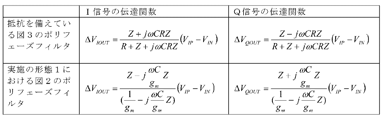
この実施の形態1のポリフェーズフィルタは、図3のポリフェーズフィルタの抵抗6a~6dが、第1のトランジスタ2a,第2のトランジスタ2b,第3のトランジスタ2c及び第4のトランジスタ2dに置き換わっている点で相違している。
このため、この実施の形態1のポリフェーズフィルタにおいても、図3のポリフェーズフィルタと同様に、IQ信号の振幅が常に一定となり、IQ信号の位相が角周波数ωで90度差となる。
したがって、この実施の形態1のポリフェーズフィルタは、図3のポリフェーズフィルタと同じIQ特性を実現することができる。
ただし、この実施の形態1のポリフェーズフィルタは、図3のポリフェーズフィルタと異なり、トランスコンダクタンスgmを有するトランジスタを用いて構成されているため、利得を持たせることが可能である。
このため、この実施の形態1のポリフェーズフィルタにおいても、図3のポリフェーズフィルタと同様に、IQ信号の振幅が常に一定となり、IQ信号の位相が角周波数ωで90度差となる。
したがって、この実施の形態1のポリフェーズフィルタは、図3のポリフェーズフィルタと同じIQ特性を実現することができる。
ただし、この実施の形態1のポリフェーズフィルタは、図3のポリフェーズフィルタと異なり、トランスコンダクタンスgmを有するトランジスタを用いて構成されているため、利得を持たせることが可能である。
この実施の形態1のポリフェーズフィルタが持つことが可能な利得は、以下の表2に示すように、トランスコンダクタンスgmとωCの大小関係によって決まる。ωは角周波数、Cは第1のコンデンサ3a、第2のコンデンサ3b、第3のコンデンサ3c及び第4のコンデンサ3dの容量値である。
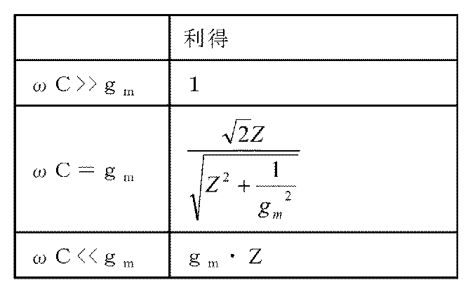
ωC=gmの場合、分子が分母よりも大きいため利得が1以上になる。また、ωC<<gmの場合も利得が1以上になる。
したがって、この実施の形態1のポリフェーズフィルタは、トランスコンダクタンスgmとωCの大小関係にかかわらず、1以上の利得を持つことが可能である。
また、この実施の形態1のポリフェーズフィルタは、角周波数がω=gm/CRで決定される。トランスコンダクタンスgmは、トランジスタを流れる電流によって決まるため、電流を可変することで、角周波数ωを可変することが可能である。したがって、この実施の形態1のポリフェーズフィルタは、特性の可変が可能なポリフェーズフィルタである。
したがって、この実施の形態1のポリフェーズフィルタは、トランスコンダクタンスgmとωCの大小関係にかかわらず、1以上の利得を持つことが可能である。
また、この実施の形態1のポリフェーズフィルタは、角周波数がω=gm/CRで決定される。トランスコンダクタンスgmは、トランジスタを流れる電流によって決まるため、電流を可変することで、角周波数ωを可変することが可能である。したがって、この実施の形態1のポリフェーズフィルタは、特性の可変が可能なポリフェーズフィルタである。
以上で明らかなように、この実施の形態1によれば、第1の入力端子1aから入力される第1のI信号VIPを増幅する第1のトランジスタ2aと、第2の入力端子1bから入力される第1のQ信号VQPを増幅する第2のトランジスタ2bと、第1のI信号VIPと差動信号を構成している第2のI信号VINが第3の入力端子1cから入力されると、第2のI信号VINを増幅する第3のトランジスタ2cと、第1のQ信号VQPと差動信号を構成している第2のQ信号VQNが第4の入力端子1dから入力されると、第2のQ信号VQNを増幅する第4のトランジスタ2dとを備えるように構成したので、通過ロスの発生を抑えることができる効果を奏する。
また、利得を有し、かつ、特性を可変することが可能なポリフェーズフィルタを得ることができる。
また、利得を有し、かつ、特性を可変することが可能なポリフェーズフィルタを得ることができる。
また、この実施の形態1によれば、第1のトランジスタ2a,第2のトランジスタ2b,第3のトランジスタ2c及び第4のトランジスタ2dのコレクタ端子のそれぞれが負荷5a,5b,5c,5dを介して電源Vccと接続されているように構成したので、第1のトランジスタ2a,第2のトランジスタ2b,第3のトランジスタ2c及び第4のトランジスタ2dとして、NPN型のバイポーラトランジスタを用いることができる。
この実施の形態1では、第1のトランジスタ2a,第2のトランジスタ2b,第3のトランジスタ2c及び第4のトランジスタ2dが、バイポーラトランジスタである例を示しているが、トランスコンダクタンスgmを有していればよく、バイポーラトランジスタに限るものではない。
このため、第1のトランジスタ2a,第2のトランジスタ2b,第3のトランジスタ2c及び第4のトランジスタ2dは、例えば、電界効果トランジスタであってもよいし、CMOS(Complementary Metal Oxide Semiconductor)などのMOSトランジスタであってもよい。
なお、第1のトランジスタ2a,第2のトランジスタ2b,第3のトランジスタ2c及び第4のトランジスタ2dが電界効果トランジスタである場合、電界効果トランジスタのゲート端子は、バイポーラトランジスタのベース端子に相当する。
また、電界効果トランジスタのドレイン端子は、バイポーラトランジスタのコレクタ端子に相当し、電界効果トランジスタのソース端子は、バイポーラトランジスタのエミッタ端子に相当する。
このため、第1のトランジスタ2a,第2のトランジスタ2b,第3のトランジスタ2c及び第4のトランジスタ2dは、例えば、電界効果トランジスタであってもよいし、CMOS(Complementary Metal Oxide Semiconductor)などのMOSトランジスタであってもよい。
なお、第1のトランジスタ2a,第2のトランジスタ2b,第3のトランジスタ2c及び第4のトランジスタ2dが電界効果トランジスタである場合、電界効果トランジスタのゲート端子は、バイポーラトランジスタのベース端子に相当する。
また、電界効果トランジスタのドレイン端子は、バイポーラトランジスタのコレクタ端子に相当し、電界効果トランジスタのソース端子は、バイポーラトランジスタのエミッタ端子に相当する。
実施の形態2.
上記実施の形態1では、第1のトランジスタ2a,第2のトランジスタ2b,第3のトランジスタ2c及び第4のトランジスタ2dのエミッタ端子が接地されている例を示している。
この実施の形態2では、第1のトランジスタ2aのエミッタ端子及び第3のトランジスタ2cのエミッタ端子が第1の電流源7aを介してグランドと接続され、第2のトランジスタ2bのエミッタ端子及び第4のトランジスタ2dのエミッタ端子が第2の電流源7bを介してグランドと接続されている例を説明する。
上記実施の形態1では、第1のトランジスタ2a,第2のトランジスタ2b,第3のトランジスタ2c及び第4のトランジスタ2dのエミッタ端子が接地されている例を示している。
この実施の形態2では、第1のトランジスタ2aのエミッタ端子及び第3のトランジスタ2cのエミッタ端子が第1の電流源7aを介してグランドと接続され、第2のトランジスタ2bのエミッタ端子及び第4のトランジスタ2dのエミッタ端子が第2の電流源7bを介してグランドと接続されている例を説明する。
図4はこの発明の実施の形態2によるポリフェーズフィルタを示す回路図である。図4において、図1及び図2と同一符号は同一または相当部分を示すので説明を省略する。
第1の電流源7aは+側が第1のトランジスタ2aのエミッタ端子及び第3のトランジスタ2cのエミッタ端子と接続され、-側がグランドと接続されている。
第2の電流源7bは+側が第2のトランジスタ2bのエミッタ端子及び第4のトランジスタ2dのエミッタ端子と接続され、-側がグランドと接続されている。
第1の電流源7aは+側が第1のトランジスタ2aのエミッタ端子及び第3のトランジスタ2cのエミッタ端子と接続され、-側がグランドと接続されている。
第2の電流源7bは+側が第2のトランジスタ2bのエミッタ端子及び第4のトランジスタ2dのエミッタ端子と接続され、-側がグランドと接続されている。
図4では、第1のトランジスタ2a,第2のトランジスタ2b,第3のトランジスタ2c及び第4のトランジスタ2dのコレクタ端子のそれぞれが負荷5a,5b,5c,5dを介して電源Vccと接続されているが、第1の出力端子4a、第2の出力端子4b、第3の出力端子4c及び第4の出力端子4dのそれぞれにトランスインピーダンスアンプなどの負荷回路が接続される場合には、負荷5a~5dが接続されている必要はない。
次に動作について説明する。
第1のI信号VIPと第2のI信号VINとの間に差動アンバランスが生じている場合でも、第1のトランジスタ2aのエミッタ端子及び第3のトランジスタ2cのエミッタ端子が第1の電流源7aを介してグランドと接続されることで、第1のトランジスタ2aを流れる電流Iaと、第3のトランジスタ2cを流れる電流Idとは差動信号になる。
また、第1のQ信号VQPと第2のQ信号VQNとの間に差動アンバランスが生じている場合でも、第2のトランジスタ2bのエミッタ端子及び第4のトランジスタ2dのエミッタ端子が第2の電流源7bを介してグランドと接続されることで、第2のトランジスタ2bを流れる電流Ifと、第4のトランジスタ2dを流れる電流Ihとは差動信号になる。
これにより、上記実施の形態1よりも、ポリフェーズフィルタによるイメージ妨害波の抑圧精度を高めることができる。
第1のI信号VIPと第2のI信号VINとの間に差動アンバランスが生じている場合でも、第1のトランジスタ2aのエミッタ端子及び第3のトランジスタ2cのエミッタ端子が第1の電流源7aを介してグランドと接続されることで、第1のトランジスタ2aを流れる電流Iaと、第3のトランジスタ2cを流れる電流Idとは差動信号になる。
また、第1のQ信号VQPと第2のQ信号VQNとの間に差動アンバランスが生じている場合でも、第2のトランジスタ2bのエミッタ端子及び第4のトランジスタ2dのエミッタ端子が第2の電流源7bを介してグランドと接続されることで、第2のトランジスタ2bを流れる電流Ifと、第4のトランジスタ2dを流れる電流Ihとは差動信号になる。
これにより、上記実施の形態1よりも、ポリフェーズフィルタによるイメージ妨害波の抑圧精度を高めることができる。
この実施の形態2では、第1のトランジスタ2aのエミッタ端子及び第3のトランジスタ2cのエミッタ端子が、第1の電流源7aを介してグランドと接続され、第2のトランジスタ2bのエミッタ端子及び第4のトランジスタ2dのエミッタ端子が、第2の電流源7bを介してグランドと接続されている例を示している。
図5に示すように、第1の電流源7aの代わりに、第1の抵抗8aが接続され、第2の電流源7bの代わりに、第2の抵抗8bが接続されていても、同様の効果を得ることができる。
図5はこの発明の実施の形態2による他のポリフェーズフィルタを示す回路図である。
図5に示すように、第1の電流源7aの代わりに、第1の抵抗8aが接続され、第2の電流源7bの代わりに、第2の抵抗8bが接続されていても、同様の効果を得ることができる。
図5はこの発明の実施の形態2による他のポリフェーズフィルタを示す回路図である。
この実施の形態2では、第1のトランジスタ2a,第2のトランジスタ2b,第3のトランジスタ2c及び第4のトランジスタ2dが、バイポーラトランジスタである例を示しているが、上記実施の形態1と同様に、例えば、電界効果トランジスタであってもよいし、CMOSなどのMOSトランジスタであってもよい。
実施の形態3.
上記実施の形態1では、第1のトランジスタ2a,第2のトランジスタ2b,第3のトランジスタ2c及び第4のトランジスタ2dのエミッタ端子が接地されている例を示している。
この実施の形態3では、第1のトランジスタ9a,第2のトランジスタ9b,第3のトランジスタ9c及び第4のトランジスタ9dのベース端子が接地されている例を説明する。
上記実施の形態1では、第1のトランジスタ2a,第2のトランジスタ2b,第3のトランジスタ2c及び第4のトランジスタ2dのエミッタ端子が接地されている例を示している。
この実施の形態3では、第1のトランジスタ9a,第2のトランジスタ9b,第3のトランジスタ9c及び第4のトランジスタ9dのベース端子が接地されている例を説明する。
図6はこの発明の実施の形態3によるポリフェーズフィルタを示す回路図である。図6において、図1及び図2と同一符号は同一または相当部分を示すので説明を省略する。
第1のトランジスタ9aはトランスコンダクタンスgmを有し、ベース端子が接地されているバイポーラトランジスタである。
第1のトランジスタ9aは、エミッタ端子が第1の入力端子1aと接続され、コレクタ端子(第1のトランジスタ9aの出力端子)が第1の出力端子4aと接続されており、第1の入力端子1aから入力された第1のI信号VIPを増幅して、増幅後の第1のI信号VIPを第1の出力端子4aに出力する。
第2のトランジスタ9bはトランスコンダクタンスgmを有し、ベース端子が接地されているバイポーラトランジスタである。
第2のトランジスタ9bは、エミッタ端子が第2の入力端子1bと接続され、コレクタ端子(第2のトランジスタ9bの出力端子)が第2の出力端子4bと接続されており、第2の入力端子1bから入力された第1のQ信号VQPを増幅して、増幅後の第1のQ信号VQPを第2の出力端子4bに出力する。
第1のトランジスタ9aはトランスコンダクタンスgmを有し、ベース端子が接地されているバイポーラトランジスタである。
第1のトランジスタ9aは、エミッタ端子が第1の入力端子1aと接続され、コレクタ端子(第1のトランジスタ9aの出力端子)が第1の出力端子4aと接続されており、第1の入力端子1aから入力された第1のI信号VIPを増幅して、増幅後の第1のI信号VIPを第1の出力端子4aに出力する。
第2のトランジスタ9bはトランスコンダクタンスgmを有し、ベース端子が接地されているバイポーラトランジスタである。
第2のトランジスタ9bは、エミッタ端子が第2の入力端子1bと接続され、コレクタ端子(第2のトランジスタ9bの出力端子)が第2の出力端子4bと接続されており、第2の入力端子1bから入力された第1のQ信号VQPを増幅して、増幅後の第1のQ信号VQPを第2の出力端子4bに出力する。
第3のトランジスタ9cはトランスコンダクタンスgmを有し、ベース端子が接地されているバイポーラトランジスタである。
第3のトランジスタ9cは、エミッタ端子が第3の入力端子1cと接続され、コレクタ端子(第3のトランジスタ9cの出力端子)が第3の出力端子4cと接続されており、第3の入力端子1cから入力された第2のI信号VINを増幅して、増幅後の第2のI信号VINを第3の出力端子4cに出力する。
第4のトランジスタ9dはトランスコンダクタンスgmを有し、ベース端子が接地されているバイポーラトランジスタである。
第4のトランジスタ9dは、エミッタ端子が第4の入力端子1dと接続され、コレクタ端子(第4のトランジスタ9dの出力端子)が第4の出力端子4dと接続されており、第4の入力端子1dから入力された第2のQ信号VQNを増幅して、増幅後の第2のQ信号VQNを第4の出力端子4dに出力する。
第3のトランジスタ9cは、エミッタ端子が第3の入力端子1cと接続され、コレクタ端子(第3のトランジスタ9cの出力端子)が第3の出力端子4cと接続されており、第3の入力端子1cから入力された第2のI信号VINを増幅して、増幅後の第2のI信号VINを第3の出力端子4cに出力する。
第4のトランジスタ9dはトランスコンダクタンスgmを有し、ベース端子が接地されているバイポーラトランジスタである。
第4のトランジスタ9dは、エミッタ端子が第4の入力端子1dと接続され、コレクタ端子(第4のトランジスタ9dの出力端子)が第4の出力端子4dと接続されており、第4の入力端子1dから入力された第2のQ信号VQNを増幅して、増幅後の第2のQ信号VQNを第4の出力端子4dに出力する。
第1の電流源10aは+側が第1のトランジスタ9aのエミッタ端子と接続され、-側がグランドと接続されている。
第2の電流源10bは+側が第2のトランジスタ9bのエミッタ端子と接続され、-側がグランドと接続されている。
第3の電流源10cは+側が第3のトランジスタ9cのエミッタ端子と接続され、-側がグランドと接続されている。
第4の電流源10dは+側が第4のトランジスタ9dのエミッタ端子と接続され、-側がグランドと接続されている。
第2の電流源10bは+側が第2のトランジスタ9bのエミッタ端子と接続され、-側がグランドと接続されている。
第3の電流源10cは+側が第3のトランジスタ9cのエミッタ端子と接続され、-側がグランドと接続されている。
第4の電流源10dは+側が第4のトランジスタ9dのエミッタ端子と接続され、-側がグランドと接続されている。
図6では、第1のトランジスタ9a,第2のトランジスタ9b,第3のトランジスタ9c及び第4のトランジスタ9dのコレクタ端子のそれぞれが負荷5a,5b,5c,5dを介して電源Vccと接続されているが、第1の出力端子4a、第2の出力端子4b、第3の出力端子4c及び第4の出力端子4dのそれぞれにトランスインピーダンスアンプなどの負荷回路が接続される場合には、負荷5a~5dが接続されている必要はない。
次に動作について説明する。
この実施の形態3のポリフェーズフィルタの動作は、上記実施の形態1のポリフェーズフィルタの動作と概ね同じである。
ただし、この実施の形態3では、第1のトランジスタ9a,第2のトランジスタ9b,第3のトランジスタ9c及び第4のトランジスタ9dのベース端子が接地されている。
このため、第1の入力端子1a,第2の入力端子1b,第3の入力端子1c及び第4の入力端子1dから見た入力インピーダンスを、第1のトランジスタ9a,第2のトランジスタ9b,第3のトランジスタ9c及び第4のトランジスタ9dにおけるインピーダンスの1/gmとすることができる。
この実施の形態3のポリフェーズフィルタの動作は、上記実施の形態1のポリフェーズフィルタの動作と概ね同じである。
ただし、この実施の形態3では、第1のトランジスタ9a,第2のトランジスタ9b,第3のトランジスタ9c及び第4のトランジスタ9dのベース端子が接地されている。
このため、第1の入力端子1a,第2の入力端子1b,第3の入力端子1c及び第4の入力端子1dから見た入力インピーダンスを、第1のトランジスタ9a,第2のトランジスタ9b,第3のトランジスタ9c及び第4のトランジスタ9dにおけるインピーダンスの1/gmとすることができる。
これにより、第1の出力端子4a,第2の出力端子4b,第3の出力端子4c及び第4の出力端子4dから見た出力インピーダンスに応じて、第1のトランジスタ9a,第2のトランジスタ9b,第3のトランジスタ9c及び第4のトランジスタ9dのトランスコンダクタンスgmを設定することで、広帯域な入出力整合を実現することができる。また、不要な整合素子を排除して、小型化を図ることができるとともに、広帯域性能を実現することができる。
この実施の形態3では、第1のトランジスタ9aのエミッタ端子が第1の電流源10aを介してグランドと接続され、第2のトランジスタ9bのエミッタ端子が第2の電流源10bを介してグランドと接続されている。また、第3のトランジスタ9cのエミッタ端子が第3の電流源10cを介してグランドと接続され、第4のトランジスタ9dのエミッタ端子が第4の電流源10dを介してグランドと接続されている。
図7に示すように、第1の電流源10aの代わりに第1の抵抗11aが接続され、第2の電流源10bの代わりに第2の抵抗11bが接続され、第3の電流源10cの代わりに第3の抵抗11cが接続され、第4の電流源10dの代わりに第4の抵抗11dが接続されていてもよい。この場合も同様の効果を得ることができる。
図7はこの発明の実施の形態3による他のポリフェーズフィルタを示す回路図である。
図7に示すように、第1の電流源10aの代わりに第1の抵抗11aが接続され、第2の電流源10bの代わりに第2の抵抗11bが接続され、第3の電流源10cの代わりに第3の抵抗11cが接続され、第4の電流源10dの代わりに第4の抵抗11dが接続されていてもよい。この場合も同様の効果を得ることができる。
図7はこの発明の実施の形態3による他のポリフェーズフィルタを示す回路図である。
この実施の形態3では、第1のトランジスタ9a,第2のトランジスタ9b,第3のトランジスタ9c及び第4のトランジスタ9dが、バイポーラトランジスタである例を示しているが、第1のトランジスタ9a,第2のトランジスタ9b,第3のトランジスタ9c及び第4のトランジスタ9dは、例えば、電界効果トランジスタであってもよいし、CMOSなどのMOSトランジスタであってもよい。
なお、本願発明はその発明の範囲内において、各実施の形態の自由な組み合わせ、あるいは各実施の形態の任意の構成要素の変形、もしくは各実施の形態において任意の構成要素の省略が可能である。
この発明は、トランジスタを備えているポリフェーズフィルタに適している。
1a 第1の入力端子、1b 第2の入力端子、1c 第3の入力端子、1d 第4の入力端子、2a 第1のトランジスタ、2b 第2のトランジスタ、2c 第3のトランジスタ、2d 第4のトランジスタ、3a 第1のコンデンサ、3b 第2のコンデンサ、3c 第3のコンデンサ、3d 第4のコンデンサ、4a 第1の出力端子、4b 第2の出力端子、4c 第3の出力端子、4d 第4の出力端子、5a~5d 負荷、6a~6d 抵抗、7a 第1の電流源、7b 第2の電流源、8a 第1の抵抗、8b 第2の抵抗、9a 第1のトランジスタ、9b 第2のトランジスタ、9c 第3のトランジスタ、9d 第4のトランジスタ、10a 第1の電流源、10b 第2の電流源、10c 第3の電流源、10d 第4の電流源、11a 第1の抵抗、11b 第2の抵抗、11c 第3の抵抗、11d 第4の抵抗。
Claims (10)
- 第1の入力端子から入力される第1のI信号を増幅する第1のトランジスタと、
第2の入力端子から入力される第1のQ信号を増幅する第2のトランジスタと、
前記第1のI信号と差動信号を構成している第2のI信号が第3の入力端子から入力されると、前記第2のI信号を増幅する第3のトランジスタと、
前記第1のQ信号と差動信号を構成している第2のQ信号が第4の入力端子から入力されると、前記第2のQ信号を増幅する第4のトランジスタと、
前記第1のトランジスタの出力端子と前記第2の入力端子との間に接続されている第1のコンデンサと、
前記第2のトランジスタの出力端子と前記第3の入力端子との間に接続されている第2のコンデンサと、
前記第3のトランジスタの出力端子と前記第4の入力端子との間に接続されている第3のコンデンサと、
前記第4のトランジスタの出力端子と前記第1の入力端子との間に接続されている第4のコンデンサと
を備えたポリフェーズフィルタ。 - 前記第1から第4のトランジスタの出力端子のそれぞれが負荷を介して電源と接続されていることを特徴とする請求項1記載のポリフェーズフィルタ。
- 前記第1から第4のトランジスタのそれぞれが、エミッタ端子が接地されているバイポーラトランジスタであり、
前記第1のトランジスタのベース端子が前記第1の入力端子と接続され、前記第1のトランジスタのコレクタ端子が前記第1のトランジスタの出力端子であり、
前記第2のトランジスタのベース端子が前記第2の入力端子と接続され、前記第2のトランジスタのコレクタ端子が前記第2のトランジスタの出力端子であり、
前記第3のトランジスタのベース端子が前記第3の入力端子と接続され、前記第3のトランジスタのコレクタ端子が前記第3のトランジスタの出力端子であり、
前記第4のトランジスタのベース端子が前記第4の入力端子と接続され、前記第4のトランジスタのコレクタ端子が前記第4のトランジスタの出力端子であることを特徴とする請求項1記載のポリフェーズフィルタ。 - 前記第1のトランジスタのエミッタ端子及び前記第3のトランジスタのエミッタ端子は、第1の電流源又は第1の抵抗を介してグランドと接続され、
前記第2のトランジスタのエミッタ端子及び前記第4のトランジスタのエミッタ端子は、第2の電流源又は第2の抵抗を介してグランドと接続されていることを特徴とする請求項3記載のポリフェーズフィルタ。 - 前記第1から第4のトランジスタのそれぞれが、ソース端子が接地されている電界効果トランジスタであり、
前記第1のトランジスタのゲート端子が前記第1の入力端子と接続され、前記第1のトランジスタのドレイン端子が前記第1のトランジスタの出力端子であり、
前記第2のトランジスタのゲート端子が前記第2の入力端子と接続され、前記第2のトランジスタのドレイン端子が前記第2のトランジスタの出力端子であり、
前記第3のトランジスタのゲート端子が前記第3の入力端子と接続され、前記第3のトランジスタのドレイン端子が前記第3のトランジスタの出力端子であり、
前記第4のトランジスタのゲート端子が前記第4の入力端子と接続され、前記第4のトランジスタのドレイン端子が前記第4のトランジスタの出力端子であることを特徴とする請求項1記載のポリフェーズフィルタ。 - 前記第1のトランジスタのソース端子及び前記第3のトランジスタのソース端子は、第1の電流源又は第1の抵抗を介してグランドと接続され、
前記第2のトランジスタのソース端子及び前記第4のトランジスタのソース端子は、第2の電流源又は第2の抵抗を介してグランドと接続されていることを特徴とする請求項5記載のポリフェーズフィルタ。 - 前記第1から第4のトランジスタのそれぞれが、ベース端子が接地されているバイポーラトランジスタであり、
前記第1のトランジスタのエミッタ端子が前記第1の入力端子と接続され、前記第1のトランジスタのコレクタ端子が前記第1のトランジスタの出力端子であり、
前記第2のトランジスタのエミッタ端子が前記第2の入力端子と接続され、前記第2のトランジスタのコレクタ端子が前記第2のトランジスタの出力端子であり、
前記第3のトランジスタのエミッタ端子が前記第3の入力端子と接続され、前記第3のトランジスタのコレクタ端子が前記第3のトランジスタの出力端子であり、
前記第4のトランジスタのエミッタ端子が前記第4の入力端子と接続され、前記第4のトランジスタのコレクタ端子が前記第4のトランジスタの出力端子であることを特徴とする請求項1記載のポリフェーズフィルタ。 - 前記第1のトランジスタのエミッタ端子は、第1の電流源又は第1の抵抗を介してグランドと接続され、
前記第2のトランジスタのエミッタ端子は、第2の電流源又は第2の抵抗を介してグランドと接続され、
前記第3のトランジスタのエミッタ端子は、第3の電流源又は第3の抵抗を介してグランドと接続され、
前記第4のトランジスタのエミッタ端子は、第4の電流源又は第4の抵抗を介してグランドと接続されていることを特徴とする請求項7記載のポリフェーズフィルタ。 - 前記第1から第4のトランジスタのそれぞれが、ゲート端子が接地されている電界効果トランジスタであり、
前記第1のトランジスタのソース端子が前記第1の入力端子と接続され、前記第1のトランジスタのドレイン端子が前記第1のトランジスタの出力端子であり、
前記第2のトランジスタのソース端子が前記第2の入力端子と接続され、前記第2のトランジスタのドレイン端子が前記第2のトランジスタの出力端子であり、
前記第3のトランジスタのソース端子が前記第3の入力端子と接続され、前記第3のトランジスタのドレイン端子が前記第3のトランジスタの出力端子であり、
前記第4のトランジスタのソース端子が前記第4の入力端子と接続され、前記第4のトランジスタのドレイン端子が前記第4のトランジスタの出力端子であることを特徴とする請求項1記載のポリフェーズフィルタ。 - 前記第1のトランジスタのソース端子は、第1の電流源又は第1の抵抗を介してグランドと接続され、
前記第2のトランジスタのソース端子は、第2の電流源又は第2の抵抗を介してグランドと接続され、
前記第3のトランジスタのソース端子は、第3の電流源又は第3の抵抗を介してグランドと接続され、
前記第4のトランジスタのソース端子は、第4の電流源又は第4の抵抗を介してグランドと接続されていることを特徴とする請求項9記載のポリフェーズフィルタ。
Priority Applications (4)
| Application Number | Priority Date | Filing Date | Title |
|---|---|---|---|
| PCT/JP2017/008239 WO2018158902A1 (ja) | 2017-03-02 | 2017-03-02 | ポリフェーズフィルタ |
| EP17898608.9A EP3565117B1 (en) | 2017-03-02 | 2017-03-02 | Method of operating polyphase filter |
| JP2017539684A JP6336217B1 (ja) | 2017-03-02 | 2017-03-02 | ポリフェーズフィルタ |
| US16/479,894 US10763826B2 (en) | 2017-03-02 | 2017-03-02 | Polyphase filter |
Applications Claiming Priority (1)
| Application Number | Priority Date | Filing Date | Title |
|---|---|---|---|
| PCT/JP2017/008239 WO2018158902A1 (ja) | 2017-03-02 | 2017-03-02 | ポリフェーズフィルタ |
Publications (1)
| Publication Number | Publication Date |
|---|---|
| WO2018158902A1 true WO2018158902A1 (ja) | 2018-09-07 |
Family
ID=62487393
Family Applications (1)
| Application Number | Title | Priority Date | Filing Date |
|---|---|---|---|
| PCT/JP2017/008239 Ceased WO2018158902A1 (ja) | 2017-03-02 | 2017-03-02 | ポリフェーズフィルタ |
Country Status (4)
| Country | Link |
|---|---|
| US (1) | US10763826B2 (ja) |
| EP (1) | EP3565117B1 (ja) |
| JP (1) | JP6336217B1 (ja) |
| WO (1) | WO2018158902A1 (ja) |
Cited By (2)
| Publication number | Priority date | Publication date | Assignee | Title |
|---|---|---|---|---|
| WO2020110196A1 (ja) * | 2018-11-27 | 2020-06-04 | 三菱電機株式会社 | ベクトル合成型移相器 |
| CN114641929A (zh) * | 2019-12-06 | 2022-06-17 | 高通股份有限公司 | 具有有源信号相位生成的移相器 |
Families Citing this family (2)
| Publication number | Priority date | Publication date | Assignee | Title |
|---|---|---|---|---|
| CN111937301A (zh) * | 2018-04-18 | 2020-11-13 | 三菱电机株式会社 | 多相滤波器 |
| CN111971898A (zh) * | 2018-04-18 | 2020-11-20 | 三菱电机株式会社 | 多相滤波器 |
Citations (6)
| Publication number | Priority date | Publication date | Assignee | Title |
|---|---|---|---|---|
| US4866397A (en) * | 1988-04-07 | 1989-09-12 | Exar Corporation | Wideband 0-90 degrees adjustable phase shifter |
| JPH0370305A (ja) * | 1989-08-10 | 1991-03-26 | Fujitsu Ltd | 光信号受信装置の等化増幅回路 |
| JPH1070418A (ja) * | 1996-08-27 | 1998-03-10 | Hitachi Denshi Ltd | 多段カスコード増幅器 |
| JPH11205047A (ja) * | 1998-01-13 | 1999-07-30 | Nec Corp | 光受信器用トランスインピーダンスアンプ |
| JP2001045080A (ja) * | 1999-07-26 | 2001-02-16 | Nippon Telegr & Teleph Corp <Ntt> | 振幅整合型ポリフェーズフィルタおよび位相振幅整合型ポリフェーズフィルタならびにイメージ抑圧型受信機 |
| JP2010021826A (ja) | 2008-07-11 | 2010-01-28 | Seiko Epson Corp | 半導体集積回路 |
Family Cites Families (4)
| Publication number | Priority date | Publication date | Assignee | Title |
|---|---|---|---|---|
| US6636085B2 (en) * | 2001-04-20 | 2003-10-21 | Nec Electronics Corporation | Phase shifter with an RC polyphase filter |
| JP2003298394A (ja) | 2002-04-05 | 2003-10-17 | Fujitsu Ltd | 相互コンダクタンス型増幅回路、相互コンダクタンス型フィルタ回路及びフィルタ処理方法 |
| JP4457294B2 (ja) | 2004-02-27 | 2010-04-28 | 株式会社村田製作所 | 可変減衰器及びそれを内蔵してなるモジュール並びに通信装置 |
| US9685931B2 (en) * | 2014-08-28 | 2017-06-20 | Qualcomm Incorporated | High accuracy millimeter wave/radio frequency wideband in-phase and quadrature generation |
-
2017
- 2017-03-02 US US16/479,894 patent/US10763826B2/en not_active Expired - Fee Related
- 2017-03-02 EP EP17898608.9A patent/EP3565117B1/en active Active
- 2017-03-02 WO PCT/JP2017/008239 patent/WO2018158902A1/ja not_active Ceased
- 2017-03-02 JP JP2017539684A patent/JP6336217B1/ja active Active
Patent Citations (6)
| Publication number | Priority date | Publication date | Assignee | Title |
|---|---|---|---|---|
| US4866397A (en) * | 1988-04-07 | 1989-09-12 | Exar Corporation | Wideband 0-90 degrees adjustable phase shifter |
| JPH0370305A (ja) * | 1989-08-10 | 1991-03-26 | Fujitsu Ltd | 光信号受信装置の等化増幅回路 |
| JPH1070418A (ja) * | 1996-08-27 | 1998-03-10 | Hitachi Denshi Ltd | 多段カスコード増幅器 |
| JPH11205047A (ja) * | 1998-01-13 | 1999-07-30 | Nec Corp | 光受信器用トランスインピーダンスアンプ |
| JP2001045080A (ja) * | 1999-07-26 | 2001-02-16 | Nippon Telegr & Teleph Corp <Ntt> | 振幅整合型ポリフェーズフィルタおよび位相振幅整合型ポリフェーズフィルタならびにイメージ抑圧型受信機 |
| JP2010021826A (ja) | 2008-07-11 | 2010-01-28 | Seiko Epson Corp | 半導体集積回路 |
Non-Patent Citations (1)
| Title |
|---|
| See also references of EP3565117A4 |
Cited By (4)
| Publication number | Priority date | Publication date | Assignee | Title |
|---|---|---|---|---|
| WO2020110196A1 (ja) * | 2018-11-27 | 2020-06-04 | 三菱電機株式会社 | ベクトル合成型移相器 |
| CN114641929A (zh) * | 2019-12-06 | 2022-06-17 | 高通股份有限公司 | 具有有源信号相位生成的移相器 |
| JP2023504356A (ja) * | 2019-12-06 | 2023-02-03 | クアルコム,インコーポレイテッド | 能動的な信号位相生成を伴う位相シフタ |
| JP7682878B2 (ja) | 2019-12-06 | 2025-05-26 | クアルコム,インコーポレイテッド | 能動的な信号位相生成を伴う位相シフタ |
Also Published As
| Publication number | Publication date |
|---|---|
| US10763826B2 (en) | 2020-09-01 |
| JP6336217B1 (ja) | 2018-06-06 |
| EP3565117A1 (en) | 2019-11-06 |
| JPWO2018158902A1 (ja) | 2019-03-14 |
| EP3565117B1 (en) | 2021-12-01 |
| US20190379356A1 (en) | 2019-12-12 |
| EP3565117A4 (en) | 2020-01-08 |
Similar Documents
| Publication | Publication Date | Title |
|---|---|---|
| US7804361B2 (en) | Low noise amplifier | |
| CN101834567B (zh) | 宽带增益可调低噪声放大器 | |
| US8648652B2 (en) | Band pass filter and calibration method for band pass filter | |
| JP6336217B1 (ja) | ポリフェーズフィルタ | |
| US6496067B1 (en) | Class AB voltage current convertor having multiple transconductance stages and its application to power amplifiers | |
| JP4871590B2 (ja) | トランスコンダクタを用いた積分器及びフィルタ回路 | |
| US20080297258A1 (en) | Variable impedance circuit; and variable impedance system, filter circuit, amplifier, and communication system using the same | |
| JP2019041155A (ja) | Ota回路及びフィルタ | |
| CN102332871A (zh) | 回转器电路、宽带放大器和无线通信设备 | |
| WO2018116825A1 (ja) | 単相差動変換回路およびその信号処理方法、並びに、受信装置 | |
| JP5605256B2 (ja) | 低雑音増幅器 | |
| JP2010021826A (ja) | 半導体集積回路 | |
| CN111903054B (zh) | 单端转差分放大器和射频接收机 | |
| KR20010006759A (ko) | 주파수 변환회로 | |
| TW202310558A (zh) | 降頻混頻器 | |
| JP6177422B2 (ja) | アクティブバラン回路及びトランス | |
| TWI637591B (zh) | Ab類放大器 | |
| JP5065280B2 (ja) | トランスコンダクタンス段の構成 | |
| WO2018229977A1 (ja) | 高周波増幅器 | |
| WO2020000424A1 (zh) | 一种运算放大器、射频电路及电子设备 | |
| KR20230102155A (ko) | 2차 고조파 트랩을 갖는 증폭기 | |
| JP2011188343A (ja) | 半導体集積回路装置 | |
| JP2012100224A (ja) | 広帯域増幅器 | |
| JP2005080194A (ja) | アクティブフィルタ回路の設計方法 | |
| CN120034145A (zh) | 正交信号产生电路和产生方法 |
Legal Events
| Date | Code | Title | Description |
|---|---|---|---|
| ENP | Entry into the national phase |
Ref document number: 2017539684 Country of ref document: JP Kind code of ref document: A |
|
| 121 | Ep: the epo has been informed by wipo that ep was designated in this application |
Ref document number: 17898608 Country of ref document: EP Kind code of ref document: A1 |
|
| ENP | Entry into the national phase |
Ref document number: 2017898608 Country of ref document: EP Effective date: 20190730 |
|
| NENP | Non-entry into the national phase |
Ref country code: DE |