WO2018158902A1 - Filtre polyphasé - Google Patents
Filtre polyphasé Download PDFInfo
- Publication number
- WO2018158902A1 WO2018158902A1 PCT/JP2017/008239 JP2017008239W WO2018158902A1 WO 2018158902 A1 WO2018158902 A1 WO 2018158902A1 JP 2017008239 W JP2017008239 W JP 2017008239W WO 2018158902 A1 WO2018158902 A1 WO 2018158902A1
- Authority
- WO
- WIPO (PCT)
- Prior art keywords
- transistor
- terminal
- signal
- input
- output terminal
- Prior art date
- Legal status (The legal status is an assumption and is not a legal conclusion. Google has not performed a legal analysis and makes no representation as to the accuracy of the status listed.)
- Ceased
Links
Images




Classifications
-
- H—ELECTRICITY
- H03—ELECTRONIC CIRCUITRY
- H03H—IMPEDANCE NETWORKS, e.g. RESONANT CIRCUITS; RESONATORS
- H03H11/00—Networks using active elements
- H03H11/02—Multiple-port networks
- H03H11/04—Frequency selective two-port networks
-
- H—ELECTRICITY
- H03—ELECTRONIC CIRCUITRY
- H03H—IMPEDANCE NETWORKS, e.g. RESONANT CIRCUITS; RESONATORS
- H03H11/00—Networks using active elements
- H03H11/02—Multiple-port networks
- H03H11/04—Frequency selective two-port networks
- H03H11/0422—Frequency selective two-port networks using transconductance amplifiers, e.g. gmC filters
-
- H—ELECTRICITY
- H03—ELECTRONIC CIRCUITRY
- H03H—IMPEDANCE NETWORKS, e.g. RESONANT CIRCUITS; RESONATORS
- H03H11/00—Networks using active elements
- H03H11/02—Multiple-port networks
- H03H11/16—Networks for phase shifting
- H03H11/20—Two-port phase shifters providing an adjustable phase shift
-
- H—ELECTRICITY
- H03—ELECTRONIC CIRCUITRY
- H03H—IMPEDANCE NETWORKS, e.g. RESONANT CIRCUITS; RESONATORS
- H03H11/00—Networks using active elements
- H03H11/02—Multiple-port networks
- H03H11/16—Networks for phase shifting
- H03H11/22—Networks for phase shifting providing two or more phase shifted output signals, e.g. n-phase output
Definitions
- the present invention relates to a polyphase filter having a transistor.
- a semiconductor integrated circuit that processes a high-frequency received signal may be used.
- a semiconductor integrated circuit constituting a super heterodyne receiver for radar it is possible to suppress an image interference wave accompanying frequency conversion of a received signal in addition to a filter capable of limiting the band of the received signal.
- a polyphase filter or the like may be used.
- Patent Document 1 below discloses a polyphase filter including a plurality of resistors and a plurality of capacitors.
- the polyphase filter is a filter that is originally used for generating a signal having a phase difference of 90 degrees, but is also a filter capable of suppressing an image interference wave.
- the frequency at which the image interference wave can be suppressed changes according to the resistance value of the resistor and the capacitance value of the capacitor.
- the center frequency Fc of the frequency capable of suppressing the image interference wave is expressed by the following expression (1).
- R is the resistance value of the resistor
- C is the capacitance value of the capacitor.
- the conventional polyphase filter is configured as described above, by controlling the resistance value R of the provided resistor, it is possible to vary the frequency at which the image interference wave can be suppressed.
- the polyphase filter is configured using a resistor, which is a passive element, there is a problem in that a passage loss occurs when suppressing an image interference wave.
- the present invention has been made to solve the above-described problems, and an object thereof is to obtain a polyphase filter that can suppress the occurrence of a passage loss.
- the polyphase filter according to the present invention includes a first transistor that amplifies the first I signal input from the first input terminal, and a first transistor that amplifies the first Q signal input from the second input terminal. And a second transistor that amplifies the second I signal when a second I signal that constitutes a differential signal with the first I signal is input from the third input terminal; When the second Q signal constituting the differential signal with the first Q signal is input from the fourth input terminal, the fourth transistor for amplifying the second Q signal, and the first transistor A first capacitor connected between the output terminal and the second input terminal; a second capacitor connected between the output terminal of the second transistor and the third input terminal; Connected between the output terminal of the third transistor and the fourth input terminal. A third capacitor being, is obtained by so and a fourth capacitor connected between the output terminal and the first input terminal of the fourth transistor.
- the first transistor that amplifies the first I signal input from the first input terminal and the second transistor that amplifies the first Q signal input from the second input terminal A third transistor for amplifying the second I signal when the second I signal constituting the differential signal with the first I signal is input from the third input terminal; When the second Q signal that constitutes the Q signal and the differential signal is input from the fourth input terminal, the fourth transistor that amplifies the second Q signal is provided. There is an effect of suppressing the generation of loss.
- FIG. 1 is a circuit diagram showing a polyphase filter according to Embodiment 1 of the present invention.
- a first input terminal 1a is a terminal to which a first I signal VIP is input.
- the second input terminal 1b is a terminal to which the first Q signal V QP is input.
- the third input terminal 1c is a terminal to which the first I signal VIP and the second I signal VIN constituting a differential signal are input.
- V IP + V IN 0.
- the fourth input terminal 1d is a terminal to which the first Q signal V QP and the second Q signal V QN constituting a differential signal are input.
- V QP + V QN 0.
- the first transistor 2a has a transconductance g m, a bipolar transistor having an emitter terminal is grounded.
- the first transistor 2a has a base terminal connected to the first input terminal 1a, a collector terminal (output terminal of the first transistor 2a) connected to the first output terminal 4a, and a first input terminal. amplifying the first I signal V IP input from 1a, and outputs a first I signal V IP after amplification to the first output terminal 4a.
- the second transistor 2b has a transconductance g m, a bipolar transistor having an emitter terminal is grounded.
- the second transistor 2b has a base terminal connected to the second input terminal 1b, a collector terminal (output terminal of the second transistor 2b) connected to the second output terminal 4b, and a second input terminal.
- the first Q signal V QP input from 1b is amplified, and the amplified first Q signal V QP is output to the second output terminal 4b.
- the third transistor 2c has a transconductance g m, a bipolar transistor having an emitter terminal is grounded.
- the third transistor 2c has a base terminal connected to the third input terminal 1c, a collector terminal (output terminal of the third transistor 2c) connected to the third output terminal 4c, and a third input terminal.
- the second I signal VIN input from 1c is amplified, and the amplified second I signal VIN is output to the third output terminal 4c.
- Fourth transistor 2d has a transconductance g m, a bipolar transistor having an emitter terminal is grounded.
- the fourth transistor 2d has a base terminal connected to the fourth input terminal 1d, a collector terminal (output terminal of the fourth transistor 2d) connected to the fourth output terminal 4d, and a fourth input terminal.
- the second Q signal V QN input from 1d is amplified, and the amplified second Q signal V QN is output to the fourth output terminal 4d.
- the first capacitor 3a is connected to the collector terminal of the first transistor 2a, and the other end is connected to the second input terminal 1b.
- the second capacitor 3b has one end connected to the collector terminal of the second transistor 2b and the other end connected to the third input terminal 1c.
- the third capacitor 3c has one end connected to the collector terminal of the third transistor 2c and the other end connected to the fourth input terminal 1d.
- the fourth capacitor 3d has one end connected to the collector terminal of the fourth transistor 2d and the other end connected to the first input terminal 1a.
- the first output terminal 4a is connected to the collector terminal of the first transistor 2a, and is a terminal for outputting the first I signal VO_IP amplified by the first transistor 2a.
- the second output terminal 4b is connected to the collector terminal of the second transistor 2b, and is a terminal for outputting the first Q signal VO_QP amplified by the second transistor 2b.
- the third output terminal 4c is connected to the collector terminal of the third transistor 2c, and is a terminal for outputting the second I signal V O_IN amplified by the third transistor 2c.
- the fourth output terminal 4d is connected to the collector terminal of the fourth transistor 2d, and is a terminal for outputting the second Q signal VO_QN amplified by the fourth transistor 2d.
- FIG. 2 is a circuit diagram showing another polyphase filter according to Embodiment 1 of the present invention.
- the polyphase filter of FIG. 2 is different from the polyphase filter of FIG. 1 in that the collector terminals (output terminals) of the first to fourth transistors are connected to the power supply Vcc through a load.
- the load 5a is a resistor having an impedance Z, one end is connected to the collector terminal of the first transistor 2a, and the other end is connected to the power supply Vcc.
- the load 5b is a resistor having an impedance Z, one end is connected to the collector terminal of the second transistor 2b, and the other end is connected to the power source Vcc.
- the load 5c is a resistor having an impedance Z, one end is connected to the collector terminal of the third transistor 2c, and the other end is connected to the power source Vcc.
- the load 5d is a resistor having an impedance Z, one end is connected to the collector terminal of the fourth transistor 2d, and the other end is connected to the power supply Vcc.
- a load circuit such as a transimpedance amplifier is connected to each of the first output terminal 4a, the second output terminal 4b, the third output terminal 4c, and the fourth output terminal 4d. When such a load circuit is connected, it is not necessary to connect the loads 5a to 5d as shown in FIG.
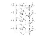
- FIG. 3 is a circuit diagram showing a conventional polyphase filter having a resistor.
- the resistor 6a is connected between the first input terminal 1a and the first output terminal 4a.
- the resistor 6b is connected between the second input terminal 1b and the second output terminal 4b.
- the resistor 6c is connected between the third input terminal 1c and the third output terminal 4c.
- the resistor 6d is connected between the fourth input terminal 1d and the fourth output terminal 4d.
- ⁇ V IOUT V O_IP ⁇ V O_IN .
- the current I a flowing through the resistor 6a is expressed by the following equation (2)
- the current I b flowing through the first capacitor 3a is expressed by the following equation (3).
- the first I signal VO_IP output from the first output terminal 4a is expressed by the following equation (4).
- R is the resistance value of the resistor 6a
- C is the capacitance value of the first capacitor 3a
- Z is the impedance of the load 5a.
- a first I signal V O_IP output from the first output terminal 4a is The following equation (5) is obtained.
- the first I signal V O_IP has been described, but the second I signal V O_IN can be obtained in the same manner.
- the second I signal V O_IN is expressed as the following equation (6).
- the differential signal ⁇ V IOUT related to the I signal is obtained.
- the differential signal ⁇ V IOUT is expressed as the following equation (7).
- ⁇ V QOUT V O_QP ⁇ V O_QN .
- the current If flowing through the resistor 6b is expressed by the following equation (8)
- the current Ie flowing through the second capacitor 3b is expressed by the following equation (9). Therefore, the first Q signal VO_QP output from the second output terminal 4b is expressed by the following equation (10).
- R is the resistance value of the resistor 6b
- C is the capacitance value of the second capacitor 3b
- Z is the impedance of the load 5b.
- the first Q signal V O_QP output from the second output terminal 4b is The following equation (11) is obtained.
- the first Q signal V O_QP has been described here, the second Q signal V O_QN can be obtained in the same manner.
- the second Q signal V O_QN is expressed as the following Expression (12).
- the differential signal ⁇ V QOUT related to the Q signal is obtained.
- the differential signal ⁇ V QOUT is expressed as the following equation (13).
- the input of the polyphase filter is short-circuited by IQ as shown in the following equation (14).
- ⁇ V IOUT V O_IP ⁇ V O_IN .
- the current I a flowing through the first transistor 2a is expressed by the following equation (17)
- the current I b flowing through the first capacitor 3a is expressed by the following equation (18). Therefore, the first I signal V O_IP output from the first output terminal 4a is expressed by the following equation (18).
- g m is the transconductance of the first transistor 2a.
- a first I signal V O_IP output from the first output terminal 4a is The following equation (20) is obtained.
- the first I signal V O_IP has been described, but the second I signal V O_IN can be obtained in the same manner.
- the second I signal V O_IN is expressed as the following Expression (21).
- the differential signal ⁇ V IOUT related to the I signal is obtained.
- the differential signal ⁇ V IOUT is expressed as the following equation (22).
- ⁇ V QOUT V O_QP ⁇ V O_QN .
- the current If flowing through the second transistor 2b is expressed by the following equation (23), and the current Ie flowing through the second capacitor 3b is expressed by the following equation (24). Therefore, the first Q signal VO_QP output from the second output terminal 4b is expressed by the following equation (25).
- the first Q signal V O_QP output from the second output terminal 4b is The following equation (26) is obtained.
- the first Q signal V O_QP has been described here, the second Q signal V O_QN can be obtained in the same manner.
- the second Q signal V O_QN is expressed as in the following Expression (27).
- the differential signal ⁇ V QOUT related to the Q signal is obtained.
- the differential signal ⁇ V QOUT is expressed as the following equation (28).
- the resistors 6a to 6d of the polyphase filter in FIG. 3 are replaced with the first transistor 2a, the second transistor 2b, the third transistor 2c, and the fourth transistor 2d. Is different. Therefore, also in the polyphase filter of the first embodiment, the amplitude of the IQ signal is always constant and the phase of the IQ signal is 90 degrees different at the angular frequency ⁇ , as in the polyphase filter of FIG. Therefore, the polyphase filter of the first embodiment can realize the same IQ characteristics as the polyphase filter of FIG. However, poly-phase filter of the first embodiment is different from the polyphase filter of Fig. 3, since it is configured using a transistor having a transconductance g m, it is possible to have a gain.
- the gain that the polyphase filter of the first embodiment can have is determined by the magnitude relationship between transconductance g m and ⁇ C, as shown in Table 2 below.
- ⁇ is an angular frequency
- C is a capacitance value of the first capacitor 3a, the second capacitor 3b, the third capacitor 3c, and the fourth capacitor 3d.
- the polyphase filter of the first embodiment can have a gain of 1 or more regardless of the magnitude relationship between transconductance g m and ⁇ C.
- the second transistor 2b that amplifies the input first Q signal V QP and the second I signal VIN that forms a differential signal with the first I signal V IP are the third input terminal 1c.
- the fourth transistor 2d for amplifying the second Q signal V QN is provided, so that it is possible to suppress the occurrence of passage loss.
- the collector terminals of the first transistor 2a, the second transistor 2b, the third transistor 2c, and the fourth transistor 2d are respectively connected via the loads 5a, 5b, 5c, and 5d.
- an NPN bipolar transistor can be used as the first transistor 2a, the second transistor 2b, the third transistor 2c, and the fourth transistor 2d.
- the first transistor 2a, the second transistor 2b, the third transistor 2c and the fourth transistor 2d is, an example is a bipolar transistor having a transconductance g m As long as it is, it is not limited to a bipolar transistor. Therefore, the first transistor 2a, the second transistor 2b, the third transistor 2c, and the fourth transistor 2d may be, for example, a field effect transistor or a MOS such as a CMOS (Complementary Metal Oxide Semiconductor). It may be a transistor.
- the gate terminal of the field effect transistor corresponds to the base terminal of the bipolar transistor.
- the drain terminal of the field effect transistor corresponds to the collector terminal of the bipolar transistor, and the source terminal of the field effect transistor corresponds to the emitter terminal of the bipolar transistor.
- Embodiment 2 FIG. In the first embodiment, an example is shown in which the emitter terminals of the first transistor 2a, the second transistor 2b, the third transistor 2c, and the fourth transistor 2d are grounded. In the second embodiment, the emitter terminal of the first transistor 2a and the emitter terminal of the third transistor 2c are connected to the ground through the first current source 7a, and the emitter terminal of the second transistor 2b and the fourth transistor An example in which the emitter terminal of the transistor 2d is connected to the ground via the second current source 7b will be described.
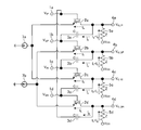
- FIG. 4 is a circuit diagram showing a polyphase filter according to Embodiment 2 of the present invention.
- the first current source 7a has a positive side connected to the emitter terminal of the first transistor 2a and the third transistor 2c, and a negative side connected to the ground.
- the second current source 7b has a positive side connected to the emitter terminal of the second transistor 2b and the fourth transistor 2d, and a negative side connected to the ground.
- the collector terminals of the first transistor 2a, the second transistor 2b, the third transistor 2c, and the fourth transistor 2d are connected to the power source Vcc through loads 5a, 5b, 5c, and 5d, respectively.
- a load circuit such as a transimpedance amplifier is connected to each of the first output terminal 4a, the second output terminal 4b, the third output terminal 4c, and the fourth output terminal 4d, the load 5a ⁇ 5d need not be connected.
- the emitter terminal of the second transistor 2b and the emitter terminal of the fourth transistor 2d are by being connected to the ground via a second current source 7b, a current I f flowing through the second transistor 2b, and the current I h flowing in the fourth transistor 2d becomes a differential signal.
- the accuracy of suppressing the image interference wave by the polyphase filter can be improved as compared with the first embodiment.
- the emitter terminal of the first transistor 2a and the emitter terminal of the third transistor 2c are connected to the ground via the first current source 7a, and the emitter terminal and the second transistor 2b of the second transistor 2b are connected.
- the emitter terminal of the fourth transistor 2d is connected to the ground via the second current source 7b.
- the first resistor 8a is connected in place of the first current source 7a
- the second resistor 8b is connected in place of the second current source 7b. An effect can be obtained.
- FIG. 5 is a circuit diagram showing another polyphase filter according to Embodiment 2 of the present invention.
- the first transistor 2a, the second transistor 2b, the third transistor 2c, and the fourth transistor 2d are bipolar transistors.
- it may be a field effect transistor or a MOS transistor such as a CMOS.
- Embodiment 3 In the first embodiment, an example is shown in which the emitter terminals of the first transistor 2a, the second transistor 2b, the third transistor 2c, and the fourth transistor 2d are grounded. In the third embodiment, an example in which the base terminals of the first transistor 9a, the second transistor 9b, the third transistor 9c, and the fourth transistor 9d are grounded will be described.
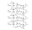
- FIG. 6 is a circuit diagram showing a polyphase filter according to Embodiment 3 of the present invention.
- the first transistor 9a has a transconductance g m, a bipolar transistor having a base terminal is grounded.
- the first transistor 9a has an emitter terminal connected to the first input terminal 1a, a collector terminal (output terminal of the first transistor 9a) connected to the first output terminal 4a, and a first input terminal. amplifying the first I signal V IP input from 1a, and outputs a first I signal V IP after amplification to the first output terminal 4a.
- the second transistor 9b has a transconductance g m, a bipolar transistor having a base terminal is grounded.
- the second transistor 9b has an emitter terminal connected to the second input terminal 1b, a collector terminal (output terminal of the second transistor 9b) connected to the second output terminal 4b, and a second input terminal.
- the first Q signal V QP input from 1b is amplified, and the amplified first Q signal V QP is output to the second output terminal 4b.
- the third transistor 9c has a transconductance g m, a bipolar transistor having a base terminal is grounded.
- the third transistor 9c has an emitter terminal connected to the third input terminal 1c, a collector terminal (an output terminal of the third transistor 9c) connected to the third output terminal 4c, and a third input terminal.
- the second I signal VIN input from 1c is amplified, and the amplified second I signal VIN is output to the third output terminal 4c.
- Fourth transistor 9d has a transconductance g m, a bipolar transistor having a base terminal is grounded.
- the fourth transistor 9d has an emitter terminal connected to the fourth input terminal 1d, a collector terminal (output terminal of the fourth transistor 9d) connected to the fourth output terminal 4d, and a fourth input terminal.
- the second Q signal V QN input from 1d is amplified, and the amplified second Q signal V QN is output to the fourth output terminal 4d.
- the first current source 10a has a positive side connected to the emitter terminal of the first transistor 9a and a negative side connected to the ground.
- the second current source 10b has a positive side connected to the emitter terminal of the second transistor 9b and a negative side connected to the ground.
- the third current source 10c has a positive side connected to the emitter terminal of the third transistor 9c and a negative side connected to the ground.
- the fourth current source 10d has a positive side connected to the emitter terminal of the fourth transistor 9d and a negative side connected to the ground.
- the collector terminals of the first transistor 9a, the second transistor 9b, the third transistor 9c, and the fourth transistor 9d are connected to the power source Vcc through loads 5a, 5b, 5c, and 5d, respectively.
- a load circuit such as a transimpedance amplifier is connected to each of the first output terminal 4a, the second output terminal 4b, the third output terminal 4c, and the fourth output terminal 4d, the load 5a ⁇ 5d need not be connected.
- the operation of the polyphase filter of the third embodiment is almost the same as the operation of the polyphase filter of the first embodiment.
- the base terminals of the first transistor 9a, the second transistor 9b, the third transistor 9c, and the fourth transistor 9d are grounded. Therefore, the input impedance viewed from the first input terminal 1a, the second input terminal 1b, the third input terminal 1c, and the fourth input terminal 1d is expressed as the first transistor 9a, the second transistor 9b, it can be 1 / g m of the impedance in the third transistor 9c and the fourth transistor 9d.
- the first transistor 9a and the second transistor 9b according to the output impedance viewed from the first output terminal 4a, the second output terminal 4b, the third output terminal 4c, and the fourth output terminal 4d.
- the transconductance g m of the third transistor 9c and the fourth transistor 9d it is possible to realize a wideband input matching. Further, unnecessary matching elements can be eliminated to achieve downsizing and wideband performance can be realized.
- the emitter terminal of the first transistor 9a is connected to the ground via the first current source 10a
- the emitter terminal of the second transistor 9b is connected to the ground via the second current source 10b. It is connected.
- the emitter terminal of the third transistor 9c is connected to the ground via the third current source 10c
- the emitter terminal of the fourth transistor 9d is connected to the ground via the fourth current source 10d.
- a first resistor 11a is connected instead of the first current source 10a
- a second resistor 11b is connected instead of the second current source 10b
- the third current source 10c instead, the third resistor 11c may be connected, and the fourth resistor 11d may be connected instead of the fourth current source 10d. In this case, the same effect can be obtained.
- FIG. 7 is a circuit diagram showing another polyphase filter according to Embodiment 3 of the present invention.
- the first transistor 9a, the second transistor 9b, the third transistor 9c, and the fourth transistor 9d are bipolar transistors.
- the first transistor 9a, The second transistor 9b, the third transistor 9c, and the fourth transistor 9d may be, for example, field effect transistors or MOS transistors such as CMOS.
- the present invention is suitable for a polyphase filter including a transistor.
Landscapes
- Networks Using Active Elements (AREA)
Abstract
L'invention concerne un filtre polyphasé comprenant : un premier transistor (2a) destiné à amplifier un premier signal I VIP à entrer depuis une première borne d'entrée (1a) ; un deuxième transistor (2b) destiné à amplifier un premier signal Q VQP à entrer depuis une deuxième borne d'entrée (1b) ; un troisième transistor (2c) destiné à amplifier un deuxième signal I VIN lorsque le deuxième signal I VIN est entré depuis une troisième borne d'entrée (1c), ce signal constituant un signal différentiel conjointement avec le premier signal I VIP ; et un quatrième transistor (2d) destiné à amplifier un deuxième signal Q VQN lorsque le deuxième signal Q VQN est entré depuis une quatrième borne d'entrée (1d), ce signal constituant un signal différentiel conjointement avec le premier signal Q V QP.
Priority Applications (4)
| Application Number | Priority Date | Filing Date | Title |
|---|---|---|---|
| US16/479,894 US10763826B2 (en) | 2017-03-02 | 2017-03-02 | Polyphase filter |
| JP2017539684A JP6336217B1 (ja) | 2017-03-02 | 2017-03-02 | ポリフェーズフィルタ |
| EP17898608.9A EP3565117B1 (fr) | 2017-03-02 | 2017-03-02 | Procédé de fonctionnement d'un filtre multiphase |
| PCT/JP2017/008239 WO2018158902A1 (fr) | 2017-03-02 | 2017-03-02 | Filtre polyphasé |
Applications Claiming Priority (1)
| Application Number | Priority Date | Filing Date | Title |
|---|---|---|---|
| PCT/JP2017/008239 WO2018158902A1 (fr) | 2017-03-02 | 2017-03-02 | Filtre polyphasé |
Publications (1)
| Publication Number | Publication Date |
|---|---|
| WO2018158902A1 true WO2018158902A1 (fr) | 2018-09-07 |
Family
ID=62487393
Family Applications (1)
| Application Number | Title | Priority Date | Filing Date |
|---|---|---|---|
| PCT/JP2017/008239 Ceased WO2018158902A1 (fr) | 2017-03-02 | 2017-03-02 | Filtre polyphasé |
Country Status (4)
| Country | Link |
|---|---|
| US (1) | US10763826B2 (fr) |
| EP (1) | EP3565117B1 (fr) |
| JP (1) | JP6336217B1 (fr) |
| WO (1) | WO2018158902A1 (fr) |
Cited By (2)
| Publication number | Priority date | Publication date | Assignee | Title |
|---|---|---|---|---|
| WO2020110196A1 (fr) * | 2018-11-27 | 2020-06-04 | 三菱電機株式会社 | Déphaseur de synthèse vectorielle |
| CN114641929A (zh) * | 2019-12-06 | 2022-06-17 | 高通股份有限公司 | 具有有源信号相位生成的移相器 |
Families Citing this family (2)
| Publication number | Priority date | Publication date | Assignee | Title |
|---|---|---|---|---|
| EP3767828B1 (fr) * | 2018-04-18 | 2022-09-21 | Mitsubishi Electric Corporation | Filtre polyphasé |
| EP3761507B1 (fr) * | 2018-04-18 | 2022-01-19 | Mitsubishi Electric Corporation | Filtre polyphasé |
Citations (6)
| Publication number | Priority date | Publication date | Assignee | Title |
|---|---|---|---|---|
| US4866397A (en) * | 1988-04-07 | 1989-09-12 | Exar Corporation | Wideband 0-90 degrees adjustable phase shifter |
| JPH0370305A (ja) * | 1989-08-10 | 1991-03-26 | Fujitsu Ltd | 光信号受信装置の等化増幅回路 |
| JPH1070418A (ja) * | 1996-08-27 | 1998-03-10 | Hitachi Denshi Ltd | 多段カスコード増幅器 |
| JPH11205047A (ja) * | 1998-01-13 | 1999-07-30 | Nec Corp | 光受信器用トランスインピーダンスアンプ |
| JP2001045080A (ja) * | 1999-07-26 | 2001-02-16 | Nippon Telegr & Teleph Corp <Ntt> | 振幅整合型ポリフェーズフィルタおよび位相振幅整合型ポリフェーズフィルタならびにイメージ抑圧型受信機 |
| JP2010021826A (ja) | 2008-07-11 | 2010-01-28 | Seiko Epson Corp | 半導体集積回路 |
Family Cites Families (4)
| Publication number | Priority date | Publication date | Assignee | Title |
|---|---|---|---|---|
| US6636085B2 (en) * | 2001-04-20 | 2003-10-21 | Nec Electronics Corporation | Phase shifter with an RC polyphase filter |
| JP2003298394A (ja) | 2002-04-05 | 2003-10-17 | Fujitsu Ltd | 相互コンダクタンス型増幅回路、相互コンダクタンス型フィルタ回路及びフィルタ処理方法 |
| JP4457294B2 (ja) | 2004-02-27 | 2010-04-28 | 株式会社村田製作所 | 可変減衰器及びそれを内蔵してなるモジュール並びに通信装置 |
| US9685931B2 (en) * | 2014-08-28 | 2017-06-20 | Qualcomm Incorporated | High accuracy millimeter wave/radio frequency wideband in-phase and quadrature generation |
-
2017
- 2017-03-02 EP EP17898608.9A patent/EP3565117B1/fr active Active
- 2017-03-02 WO PCT/JP2017/008239 patent/WO2018158902A1/fr not_active Ceased
- 2017-03-02 US US16/479,894 patent/US10763826B2/en not_active Expired - Fee Related
- 2017-03-02 JP JP2017539684A patent/JP6336217B1/ja active Active
Patent Citations (6)
| Publication number | Priority date | Publication date | Assignee | Title |
|---|---|---|---|---|
| US4866397A (en) * | 1988-04-07 | 1989-09-12 | Exar Corporation | Wideband 0-90 degrees adjustable phase shifter |
| JPH0370305A (ja) * | 1989-08-10 | 1991-03-26 | Fujitsu Ltd | 光信号受信装置の等化増幅回路 |
| JPH1070418A (ja) * | 1996-08-27 | 1998-03-10 | Hitachi Denshi Ltd | 多段カスコード増幅器 |
| JPH11205047A (ja) * | 1998-01-13 | 1999-07-30 | Nec Corp | 光受信器用トランスインピーダンスアンプ |
| JP2001045080A (ja) * | 1999-07-26 | 2001-02-16 | Nippon Telegr & Teleph Corp <Ntt> | 振幅整合型ポリフェーズフィルタおよび位相振幅整合型ポリフェーズフィルタならびにイメージ抑圧型受信機 |
| JP2010021826A (ja) | 2008-07-11 | 2010-01-28 | Seiko Epson Corp | 半導体集積回路 |
Non-Patent Citations (1)
| Title |
|---|
| See also references of EP3565117A4 |
Cited By (4)
| Publication number | Priority date | Publication date | Assignee | Title |
|---|---|---|---|---|
| WO2020110196A1 (fr) * | 2018-11-27 | 2020-06-04 | 三菱電機株式会社 | Déphaseur de synthèse vectorielle |
| CN114641929A (zh) * | 2019-12-06 | 2022-06-17 | 高通股份有限公司 | 具有有源信号相位生成的移相器 |
| JP2023504356A (ja) * | 2019-12-06 | 2023-02-03 | クアルコム,インコーポレイテッド | 能動的な信号位相生成を伴う位相シフタ |
| JP7682878B2 (ja) | 2019-12-06 | 2025-05-26 | クアルコム,インコーポレイテッド | 能動的な信号位相生成を伴う位相シフタ |
Also Published As
| Publication number | Publication date |
|---|---|
| EP3565117A4 (fr) | 2020-01-08 |
| JPWO2018158902A1 (ja) | 2019-03-14 |
| US10763826B2 (en) | 2020-09-01 |
| JP6336217B1 (ja) | 2018-06-06 |
| EP3565117A1 (fr) | 2019-11-06 |
| US20190379356A1 (en) | 2019-12-12 |
| EP3565117B1 (fr) | 2021-12-01 |
Similar Documents
| Publication | Publication Date | Title |
|---|---|---|
| US7804361B2 (en) | Low noise amplifier | |
| CN101834567B (zh) | 宽带增益可调低噪声放大器 | |
| JP6336217B1 (ja) | ポリフェーズフィルタ | |
| US6496067B1 (en) | Class AB voltage current convertor having multiple transconductance stages and its application to power amplifiers | |
| JP4871590B2 (ja) | トランスコンダクタを用いた積分器及びフィルタ回路 | |
| US20080297258A1 (en) | Variable impedance circuit; and variable impedance system, filter circuit, amplifier, and communication system using the same | |
| JP2019041155A (ja) | Ota回路及びフィルタ | |
| CN102332871A (zh) | 回转器电路、宽带放大器和无线通信设备 | |
| WO2018116825A1 (fr) | Circuit de conversion différentielle à phase unique, procédé de traitement de signal associé et dispositif de réception | |
| KR100371876B1 (ko) | 주파수 변환회로 | |
| JP5605256B2 (ja) | 低雑音増幅器 | |
| JP2010021826A (ja) | 半導体集積回路 | |
| CN111903054B (zh) | 单端转差分放大器和射频接收机 | |
| TW202310558A (zh) | 降頻混頻器 | |
| JP6177422B2 (ja) | アクティブバラン回路及びトランス | |
| JP5065280B2 (ja) | トランスコンダクタンス段の構成 | |
| WO2018229977A1 (fr) | Amplificateur à haute fréquence | |
| WO2020000424A1 (fr) | Amplificateur opérationnel, circuit de radiofréquence et dispositif électronique | |
| JP5205403B2 (ja) | 半導体集積回路装置 | |
| KR20230102155A (ko) | 2차 고조파 트랩을 갖는 증폭기 | |
| TWI637591B (zh) | Ab類放大器 | |
| JP2012100224A (ja) | 広帯域増幅器 | |
| JP2005080194A (ja) | アクティブフィルタ回路の設計方法 | |
| CN120034145A (zh) | 正交信号产生电路和产生方法 | |
| JP2013223118A (ja) | ミキサ回路 |
Legal Events
| Date | Code | Title | Description |
|---|---|---|---|
| ENP | Entry into the national phase |
Ref document number: 2017539684 Country of ref document: JP Kind code of ref document: A |
|
| 121 | Ep: the epo has been informed by wipo that ep was designated in this application |
Ref document number: 17898608 Country of ref document: EP Kind code of ref document: A1 |
|
| ENP | Entry into the national phase |
Ref document number: 2017898608 Country of ref document: EP Effective date: 20190730 |
|
| NENP | Non-entry into the national phase |
Ref country code: DE |