WO2018180902A1 - Unité d'irradiation et dispositif d'irradiation - Google Patents
Unité d'irradiation et dispositif d'irradiation Download PDFInfo
- Publication number
- WO2018180902A1 WO2018180902A1 PCT/JP2018/011455 JP2018011455W WO2018180902A1 WO 2018180902 A1 WO2018180902 A1 WO 2018180902A1 JP 2018011455 W JP2018011455 W JP 2018011455W WO 2018180902 A1 WO2018180902 A1 WO 2018180902A1
- Authority
- WO
- WIPO (PCT)
- Prior art keywords
- light emitting
- irradiation
- light
- irradiation unit
- mounting
- Prior art date
- Legal status (The legal status is an assumption and is not a legal conclusion. Google has not performed a legal analysis and makes no representation as to the accuracy of the status listed.)
- Ceased
Links
Images


Classifications
-
- F—MECHANICAL ENGINEERING; LIGHTING; HEATING; WEAPONS; BLASTING
- F21—LIGHTING
- F21S—NON-PORTABLE LIGHTING DEVICES; SYSTEMS THEREOF; VEHICLE LIGHTING DEVICES SPECIALLY ADAPTED FOR VEHICLE EXTERIORS
- F21S2/00—Systems of lighting devices, not provided for in main groups F21S4/00 - F21S10/00 or F21S19/00, e.g. of modular construction
-
- F—MECHANICAL ENGINEERING; LIGHTING; HEATING; WEAPONS; BLASTING
- F21—LIGHTING
- F21V—FUNCTIONAL FEATURES OR DETAILS OF LIGHTING DEVICES OR SYSTEMS THEREOF; STRUCTURAL COMBINATIONS OF LIGHTING DEVICES WITH OTHER ARTICLES, NOT OTHERWISE PROVIDED FOR
- F21V29/00—Protecting lighting devices from thermal damage; Cooling or heating arrangements specially adapted for lighting devices or systems
- F21V29/50—Cooling arrangements
- F21V29/502—Cooling arrangements characterised by the adaptation for cooling of specific components
- F21V29/503—Cooling arrangements characterised by the adaptation for cooling of specific components of light sources
-
- F—MECHANICAL ENGINEERING; LIGHTING; HEATING; WEAPONS; BLASTING
- F21—LIGHTING
- F21V—FUNCTIONAL FEATURES OR DETAILS OF LIGHTING DEVICES OR SYSTEMS THEREOF; STRUCTURAL COMBINATIONS OF LIGHTING DEVICES WITH OTHER ARTICLES, NOT OTHERWISE PROVIDED FOR
- F21V29/00—Protecting lighting devices from thermal damage; Cooling or heating arrangements specially adapted for lighting devices or systems
- F21V29/50—Cooling arrangements
- F21V29/56—Cooling arrangements using liquid coolants
-
- F—MECHANICAL ENGINEERING; LIGHTING; HEATING; WEAPONS; BLASTING
- F21—LIGHTING
- F21V—FUNCTIONAL FEATURES OR DETAILS OF LIGHTING DEVICES OR SYSTEMS THEREOF; STRUCTURAL COMBINATIONS OF LIGHTING DEVICES WITH OTHER ARTICLES, NOT OTHERWISE PROVIDED FOR
- F21V29/00—Protecting lighting devices from thermal damage; Cooling or heating arrangements specially adapted for lighting devices or systems
- F21V29/50—Cooling arrangements
- F21V29/60—Cooling arrangements characterised by the use of a forced flow of gas, e.g. air
- F21V29/67—Cooling arrangements characterised by the use of a forced flow of gas, e.g. air characterised by the arrangement of fans
-
- F—MECHANICAL ENGINEERING; LIGHTING; HEATING; WEAPONS; BLASTING
- F21—LIGHTING
- F21V—FUNCTIONAL FEATURES OR DETAILS OF LIGHTING DEVICES OR SYSTEMS THEREOF; STRUCTURAL COMBINATIONS OF LIGHTING DEVICES WITH OTHER ARTICLES, NOT OTHERWISE PROVIDED FOR
- F21V29/00—Protecting lighting devices from thermal damage; Cooling or heating arrangements specially adapted for lighting devices or systems
- F21V29/50—Cooling arrangements
- F21V29/70—Cooling arrangements characterised by passive heat-dissipating elements, e.g. heat-sinks
- F21V29/74—Cooling arrangements characterised by passive heat-dissipating elements, e.g. heat-sinks with fins or blades
- F21V29/76—Cooling arrangements characterised by passive heat-dissipating elements, e.g. heat-sinks with fins or blades with essentially identical parallel planar fins or blades, e.g. with comb-like cross-section
-
- F—MECHANICAL ENGINEERING; LIGHTING; HEATING; WEAPONS; BLASTING
- F21—LIGHTING
- F21V—FUNCTIONAL FEATURES OR DETAILS OF LIGHTING DEVICES OR SYSTEMS THEREOF; STRUCTURAL COMBINATIONS OF LIGHTING DEVICES WITH OTHER ARTICLES, NOT OTHERWISE PROVIDED FOR
- F21V7/00—Reflectors for light sources
- F21V7/04—Optical design
- F21V7/08—Optical design with elliptical curvature
Definitions
- the present invention relates to an irradiation unit and an irradiation apparatus.
- a plurality of LEDs arranged in a row and a reflecting member that reflects the light of these LEDs are provided, and a plurality of light source units that emit linear light are provided.
- Each light source unit has an axis on which the linear light extends.
- an irradiation device that is arranged in a direction orthogonal to a direction and that irradiates an irradiation target object by superimposing linear lights (see, for example, Patent Document 1).
- a plurality of LEDs arranged in a line, a reflecting member that reflects the light of these LEDs toward a predetermined focal point, and a rod lens that condenses the direct light component of these LEDs at a predetermined focal point of the reflecting member;
- an irradiation apparatus that irradiates an irradiation object with linear light that is condensed at a predetermined focal point (see, for example, Patent Document 2). These irradiation apparatuses are widely used in various apparatuses such as a printing apparatus and a film manufacturing apparatus.
- the installation space of the irradiation apparatus may be narrow.
- the width dimension in the direction orthogonal to the axial direction of the linear light is not suitable for the installation space, and it may be difficult to fit the irradiation apparatus in the installation space of the installation destination apparatus. is there.
- the configuration in which the LED arrangement density is increased to increase the peak illuminance it is necessary to increase the cooling performance of the LED, which leads to an increase in the size of the irradiation device.
- An object of the present invention is to provide an irradiation unit and an irradiation apparatus that can increase peak illuminance and can save space.
- the present invention relates to an irradiation unit that irradiates light to a predetermined irradiation position, each of which has a light emitting unit including a light emitting element, and a pair of mounting substrates disposed so that the light emitting units face each other, and the mounting substrate
- a light emitting unit including a light emitting element
- a pair of mounting substrates disposed so that the light emitting units face each other, and the mounting substrate
- Each of the light emitting units, and a pair of first reflecting surfaces and a second reflecting surface for controlling the light distribution of the light emitting units at the facing positions, and each of the second reflecting surfaces.
- the first reflection surface is located closer to the predetermined irradiation position than the first reflection surface, and is spaced apart from the first reflection surface from the light emission portion at the opposite position to the other light emission portion, and the first reflection surface;
- a light is disposed between each of the light emitting units and is incident on the second reflecting surface at an opposing position, and is incident on the second reflecting surface through the space.
- the present invention is characterized in that, in the irradiation unit, the pair of second reflecting surfaces are spaced apart from each other according to the separation distance of the pair of mounting substrates.
- the present invention is characterized in that, in the irradiation unit, the pair of mounting boards are arranged in parallel to each other.
- the present invention is characterized in that, in the irradiation unit, all light in a range of a predetermined radiation angle of the light emitting unit is incident on either the first reflection surface or the second reflection surface.
- the present invention is characterized in that, in the irradiation unit, a plurality of the light emitting elements are arranged in a row in the light emitting portion, and the light is irradiated linearly toward the predetermined irradiation position.
- the present invention is characterized in that, in the irradiation unit, the first reflection surface and the second reflection surface are elliptical reflection surfaces for condensing the light of the light emitting unit at a facing position at the predetermined irradiation position. .
- the first reflection surface is an elliptical reflection surface that condenses the light emitting unit at the opposed position to the predetermined irradiation position
- the second reflection surface is a flat surface or the first reflection surface. It is characterized by a curved surface different from one reflecting surface.
- the present invention provides the irradiation unit, wherein the mounting substrate, a wiring pattern for wiring the plurality of light emitting elements arranged in a line on the mounting surface of the mounting substrate, and the mounting surface of the mounting substrate are overlapped, A plate having an emission opening surrounding the plurality of light emitting elements arranged on the substrate, and the plurality of light emitting elements are electrically connected in parallel for each predetermined number,
- the wiring pattern includes a series connection wiring portion that electrically connects light emitting element groups of the light emitting elements that are electrically connected in parallel with each other, and the series connection wiring portion includes two adjacent light emitting element groups.
- a wire bonding portion of the light emitting element is inverted for each of the light emitting element groups, and each of the series connection wiring portions is adjacent to the two light emitting elements. It is characterized by being arranged at the inverted position for each group.
- the light emitting element group includes a diode element for preventing the application of an overvoltage to each light emitting element, and the series connection wiring portion has a recess.
- the diode element is disposed in the recess.
- the present invention is characterized in that, in the irradiation unit, the mounting substrate is provided with a positioning portion that engages and positions the plate.
- the present invention is characterized in that the irradiation unit includes a light-transmitting cover member that closes the exit opening.
- the present invention is characterized in that the irradiation unit includes a holding member that holds the cover member with an elastic force at an emission opening of the plate.
- the present invention is characterized in that, in the irradiation unit, a reflection surface for collimating the light of the light emitting element is provided on the inner peripheral surface of the emission opening of the plate.
- the present invention is characterized in that, in the irradiation unit, the cover member includes a lens unit for controlling transmitted light.
- the present invention includes a plurality of irradiation units according to any one of the above, and a cooling unit that cools each of the irradiation units, each of the irradiation units is connected and the cooling unit includes the irradiation unit.
- an irradiation apparatus characterized in that cooling air is blown to each of the units to cool the air, or cooling is performed through each of the irradiation units.
- the cooling unit in the irradiation apparatus, includes a tube body that extends over each of the irradiation units and into which the outside air is introduced, and a blowing hole that blows the outside air is provided on the tube body. It is provided for each unit.
- each of the irradiation units includes a base body to which the mounting substrate is attached, and the base body is an integrally molded product including a radiation fin to which the cooling air is blown. It is characterized by.
- the present invention is characterized in that, in the irradiation apparatus, the heat dissipating fins are provided in parallel to the cooling air blowing direction.
- peak illuminance can be increased and space saving can be achieved.
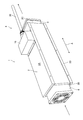
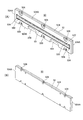
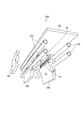
- FIG. 1 is a side view showing a configuration of an ultraviolet irradiation apparatus according to an embodiment of the present invention.
- FIG. 2 is an exploded perspective view of the ultraviolet irradiation device.
- FIG. 3 is a diagram showing an internal configuration of the ultraviolet irradiation device.
- FIG. 4 is a perspective view showing the configuration of the irradiation unit.
- FIG. 5 is a schematic view of the irradiation unit as seen from the fan mounting direction of the housing.
- FIG. 6 is an explanatory diagram of light distribution control of the irradiation unit.
- 7A and 7B are perspective views of the light emitting module, where FIG. 7A is a perspective view of the front surface, and FIG. 7B is a perspective view of the back surface.
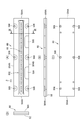
- FIG. 8A and 8B are diagrams illustrating a configuration of the light emitting module, where FIG. 8A is a plan view, FIG. 8B is a front view, FIG. 8C is a bottom view, and FIG. FIG. 9 is a cross-sectional view taken along the line IX-IX in FIG.
- FIG. 10 is an exploded perspective view of the light emitting module.
- FIG. 11 is a diagram schematically showing a cross-sectional configuration of the light emitting module.
- FIG. 12 is a diagram schematically illustrating an electrical configuration of the light emitting module.
- FIG. 13 is a diagram illustrating a wiring pattern of the light emitting module.
- FIG. 14 is an enlarged view of a portion X in FIG. FIG.
- FIG. 15 is a diagram showing a configuration of an irradiation unit according to the first modification of the present invention.
- FIG. 16 is a diagram showing a configuration of an irradiation unit according to the second modification of the present invention.
- FIG. 17 is a diagram showing a configuration of an irradiation unit according to the third modification of the present invention.
- FIG. 18 is a diagram showing a configuration of a light emitting module according to a fourth modification of the present invention.
- FIG. 19 is a cross-sectional view showing a configuration of a light emitting module according to a fifth modification of the present invention.
- FIG. 20 is a diagram showing the configuration of the mounting surface of the mounting board according to the sixth modification of the present invention.
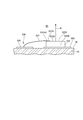
- FIG. 1 is a side view showing a configuration of an ultraviolet irradiation device 1 according to the present embodiment.
- the ultraviolet irradiation device 1 is incorporated as an inter-deck UV drying device in a built-in space provided in an offset printing device using ultraviolet curable ink, and ultraviolet curable ink applied to the printing surface W (FIG. 5) of the printed matter is ultraviolet-rayed. Cure by irradiation.
- the ultraviolet irradiation device 1 of this embodiment includes a housing 2, a power supply mechanism 4, an intake fan 6, and an exhaust fan 8.
- the housing 2 is a rectangular parallelepiped case extending in the width direction of the printed material (direction perpendicular to the transport direction), and is disposed in the offset printing apparatus with the bottom surface 2D facing the printed surface of the printed material.
- the power supply mechanism 4 is a mechanism for supplying external power to the housing 2, and is provided on the top surface 2 ⁇ / b> A of the housing 2.
- the intake fan 6 and the exhaust fan 8 are air blowing means for flowing cooling air into the housing 2.
- the intake fan 6 is provided on one side surface 2B of the housing 2, and the exhaust fan 8 is provided on the other side surface 2C. Is provided. By operating the intake fan 6 and the exhaust fan 8, cooling air flows in the longitudinal direction A of the housing 2, and the inside of the housing 2 is air-cooled.
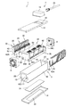
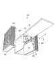
- FIG. 2 is an exploded perspective view of the ultraviolet irradiation device 1.
- the housing 2 includes a case main body 10, a top plate 12, and a bottom plate 14.
- the case main body 10 is a rectangular parallelepiped box that is open on the top surface side, and fan mounting holes 15 are formed on the side surfaces 2C and 2B on both sides.
- An exhaust fan 8 is attached.
- the top plate 12 is a member that closes the top side of the case body 10, and the top plate 12 has a mounting opening 16 to which the power supply mechanism 4 is attached.
- the power supply mechanism 4 includes a mounting box 18 attached to the mounting opening 16 and a power supply cable 20 connected to the mounting box 18 and transmitting external power.
- the bottom plate 14 is a member attached to the bottom surface 10D of the case body 10.
- An exit opening 22 is formed in the bottom plate 14 at a position corresponding to the light passage hole 17 opened in the bottom surface 10 ⁇ / b> D of the case body 10.
- the light passage hole 17 and the emission opening 22 are formed in a rectangular shape that is long in the longitudinal direction A of the housing 2, and linear ultraviolet rays extending in the longitudinal direction A (FIG. 1) are transmitted through the light passage hole 17, and The light is emitted through the emission opening 22.
- a quartz cover glass 24 that closes the light passage hole 17 and the emission opening 22 is provided between the case body 10 and the bottom plate 14.
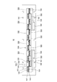
- FIG. 3 is a diagram showing an internal configuration of the ultraviolet irradiation device 1.
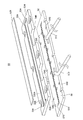
- a plurality of (three in the illustrated example) irradiation units 30 and mounting members 32 to which these irradiation units 30 are attached are housed in the housing 2.
- the attachment member 32 is a member that holds each of the irradiation units 30 in a connected state in the longitudinal direction A of the housing 2.
- the mounting member 32 includes a pair of side plates 34B and 34C that are disposed facing the side surfaces 2B and 2C of the housing 2, a pair of support columns 36 and 36 that extend between the side plates 34B and 34C, and a mounting plate. 62, and the irradiation unit 30 is fixed to the mounting plate 62.
- the mounting member 32 includes the support columns 36 and 36 as cooling means for guiding cooling air to each irradiation unit 30 and cooling it by air.
- the columns 36 and 36 are hollow tubes that are disposed on the bottom surface side of the irradiation unit 30 and extend over each of the irradiation units 30, and the side plate 34 ⁇ / b> B to which the columns 36 and 36 are connected.
- the support columns 36 and 36 are formed with a large number of blow holes 40 on the surface 36A facing the irradiation unit 30, and the cooling air introduced from the inlet 38 enters the irradiation unit 30 facing the facing surface 36A. It blows out from the blowing hole 40 toward, and each irradiation unit 30 is air-cooled with cooling air.
- each irradiation unit 30 is provided with a large number of rectangular fin-shaped radiation fins 42 disposed at the respective positions of the blowout holes 40.
- the blown cooling air is blown out.
- each irradiation unit 30 is efficiently cooled by the cooling air thermally independent from each other.
- each plate surface 42B of the radiation fin 42 is provided in parallel with the blowing direction B of the cooling air (the direction from the bottom surface 2D of the housing 2 toward the top surface 2A). Mixing of the cooling air blown out from the holes 40 is suppressed until the cooling fins 42 are removed. Thereby, the thermal independence of the cooling air for each irradiation unit 30 is enhanced.
- the inside of the housing 2 is partitioned by the side plate 34 ⁇ / b> B on the side of the intake fan 6, so that almost all of the outside air taken in by the intake fan 6 is introduced into the columns 36 and 36. It has become.
- the ends of the support columns 36, 36 on the exhaust fan 8 side are closed by the side plate 34C, and all the cooling air introduced from the introduction port 38 is blown out from the blowing hole 40 and used for air cooling of the irradiation unit 30.
- the balance of the rotational speeds (intake capacity and exhaust capacity) of the intake fan 6 and the exhaust fan 8 is adjusted so that the air volume from the blowout holes 40 of the support columns 36 and 36 is substantially uniform. Thereby, each irradiation unit 30 will be air-cooled by the cooling air which became thermally independent mutually, and also by the substantially equal air volume.
- a ventilation space 39 is provided on the side of the top surface 2 ⁇ / b> A so as to extend substantially in the center in the longitudinal direction A and reach the exhaust fan 8. Cooling air blown out in the blowing direction B from each blowing hole 40 reaches the ventilation space 39 through between the radiation fins 42, flows through the ventilation space 39, and is quickly exhausted to the outside from the exhaust fan 8.
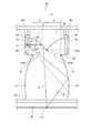
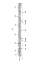
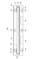
- FIG. 4 is a perspective view showing the configuration of the irradiation unit 30, and FIG. 5 is a schematic view of the irradiation unit 30 as viewed from the fan mounting direction of the housing 2.
- the irradiation unit 30 includes a pair of base bodies 50, a pair of light emitting modules 80 having a light emitting unit 60 and a mounting substrate 52, and a pair of first units facing the light emitting unit 60.
- the irradiation unit 30 is provided with a second reflecting surface 57 (described later) facing the light emitting unit 60 on each of the pair of base bodies 50. Then, each ultraviolet ray of the light emitting unit 60 is subjected to light distribution control by the first reflecting surface 55 and the second reflecting surface 57 at the opposing positions, and the unit optical axis toward the predetermined irradiation position T on the unit optical axis K. Irradiated in a line extending in a direction perpendicular to K.
- each of the plurality of irradiation units 30 is attached to the mounting member 32 and connected, and the irradiation light of each irradiation unit 30 is connected linearly on the printing surface W.
- the printing surface W is irradiated with linear ultraviolet rays having a desired length (in this embodiment, a length that crosses the printing surface W).
- each of the pair of base bodies 50 includes a board attachment surface 56 that is an attachment part of the mounting board 52 of the light emitting module 80, and as shown in FIG. 5.
- the second reflection surface 57 that is a reflection portion and the above-described many heat radiation fins 42 that are heat dissipation portions are provided.
- the substrate mounting surface 56 is a flat portion parallel to the substantially rectangular optical axis K extending in the longitudinal direction A of the housing 2, and the mounting substrate 52 is mounted substantially parallel to the substrate mounting surface 56.
- the mounting substrate 52 is a long rectangular substrate, and a light emitting unit 60 is provided on the mounting surface 58 as shown in FIG.
- the light emitting unit 60 has a number of LED chips 522 (FIG. 10) of ultraviolet LEDs arranged in a line along the direction in which the mounting substrate 52 extends, and emits ultraviolet rays linearly by the light emission of each LED chip 522. .
- the light emitting unit optical axis P which is the optical axis of the light emitting unit 60, is substantially perpendicular to the mounting surface 58 as shown in FIG.
- the pair of mounting boards 52 are arranged so that the light emitting parts 60 face each other with the unit optical axis K interposed therebetween, and the mounting surfaces 58 of the mounting boards 52 are arranged in parallel. They are perpendicular to the optical axis K and are located on the same axis E1.
- the second reflecting surface 57 is a reflecting surface extending along the extending direction of the light emitting unit 60 (longitudinal direction A of the housing 2), and is more than the light emitting unit 60 and the first reflecting surface 55 of the mounting substrate 52.
- Light distribution control is performed on the ultraviolet rays that are provided near the predetermined irradiation position T and emitted from the light emitting unit 60 at the opposite position.
- the radiation fins 42 are provided on the back side of the board mounting surface 56 in the longitudinal direction A, and radiate heat transferred from the mounting board 52 to the board mounting surface 56.
- Each of the radiation fins 42 has a substantially rectangular shape in which the lower end portion 42A extends to the back side of the second reflection surface 57, and also dissipates heat given to the second reflection surface 57 by ultraviolet irradiation.
- the base body 50 is made of a highly thermally conductive material such as aluminum, and is an integrally molded product having the above-described substrate mounting surface 56, second reflecting surface 57, and a large number of heat radiation fins 42. Thereby, compared with the case where the radiation fin 42 is formed by another member, for example, the thermal resistance between the board mounting surface 56 and the second reflection surface 57 and the radiation fin 42 can be suppressed, so that high heat radiation performance can be obtained. ing.
- the upper end portions 42C of the respective radiation fins 42 protrude from the board mounting surface 56 toward the top surface 2A of the housing 2.
- the ventilation space 39 inside the housing 2 is formed between the upper end portions 42 ⁇ / b> C of the radiation fins 42 of the pair of base bodies 50.
- the first reflector 54 is a reflector that is provided between the pair of mounting substrates 52, extends in the longitudinal direction A of the housing 2, and is convex toward the predetermined irradiation position T.
- the mounting plate 62 is a rectangular plate member that is disposed in the ventilation space 39 between the pair of base bodies 50 and extends in the longitudinal direction A of the housing 2, and as shown in FIG. 2, the side plate of the mounting member 32. It is supported by 34B and 34C.
- the mounting plate 62 is provided with a terminal block 64 for each irradiation unit 30 on the surface opposite to the surface on which the first reflector 54 is mounted. Connected.
- the mounting plate 62 may be held by the pair of base bodies 50 instead of the mounting member 32.
- each of the first reflecting surfaces 55 is a reflecting surface extending along the extending direction of the light emitting unit 60 (the longitudinal direction A), and controls the light distribution of ultraviolet rays emitted from the light emitting unit 60 at the opposite position.
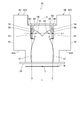
- FIG. 6 is an explanatory diagram of the light distribution control of the irradiation unit 30.
- the light emitting unit 60 of the light emitting module 80 has a predetermined radiation angle ⁇ centered on the light emitting unit optical axis P, and the irradiation unit 30 has substantially all the radiation angles ⁇ within the range.
- Ultraviolet rays are subjected to light distribution control by the first reflecting surface 55 and the second reflecting surface 57 at the position facing the light emitting unit 60. Specifically, the ultraviolet rays in the first range ⁇ 1 of the radiation angle ⁇ are incident on the first reflecting surface 55 and light distribution is controlled, and the remaining ultraviolet rays in the second range ⁇ 2 are incident on the second reflecting surface 57. Light distribution is controlled.
- the lower end portion 55A of the first reflecting surface 55 and the upper end portion 57A of the second reflecting surface 57 are positioned on a straight line E2 that divides the first range ⁇ 1 and the second range ⁇ 2. All the ultraviolet rays having the radiation angle ⁇ are incident on one of the first reflecting surface 55 and the second reflecting surface 57.
- the first reflecting surface 55 and the second reflecting surface 57 at the opposing positions of one mounting substrate 52 are not physically continuous, and as shown in FIG.
- the second reflecting surface 57 located near the predetermined irradiation position T with respect to 55 is arranged at a distance S from the first reflecting surface 55 toward the light emitting unit 60 side of the other mounting substrate 52. Yes. With the separation of the distance S, a space Q is opened between the first reflecting surface 55 and the second reflecting surface 57.
- the ultraviolet rays in the second range ⁇ 2 radiated from the respective mounting substrates 52 are not shielded by the second reflecting surface 57 disposed on the same side as the mounting substrate 52, and the space Q is not blocked. Then, the light is incident on the second reflecting surface 57 at the position facing the mounting substrate 52, and the light distribution is controlled.
- each of the pair of second reflecting surfaces 57 is thus spaced apart from the first reflecting surface 55 with the space Q therebetween, so the first reflecting surface 55 and the second reflecting surface 57 are separated.
- the width of the irradiation unit 30 is narrower than the configuration in which is a continuous reflecting surface.
- the first reflecting surface 55 and the second reflecting surface 57 are one continuous reflecting surface
- the first reflecting surface 55 of each of the first reflectors 54 is determined by the amount corresponding to the second reflecting surface 57. It extends to the irradiation position T side, and the width of the first reflector 54 is increased accordingly.
- the width of the first reflector 54 is suppressed by the amount corresponding to the second reflecting surface 57, so that the width of the irradiation unit 30 is reduced.
- each of the pair of second reflecting surfaces 57 is spaced apart from the pair of mounting boards 52 by a distance substantially equal to the distance L.
- the width of the irradiation unit 30 is narrower than that in which both the mounting substrates 52 are inclined.
- the first reflection surface 55 and the second reflection surface 57 are configured as a condensing reflection surface that condenses the ultraviolet rays of the light emitting unit 60 at the opposed positions at a predetermined irradiation position T. ing.
- the first reflection surface 55 and the second reflection surface 57 are formed on elliptical reflection surfaces in which the first focal point f1 is set to the light emitting unit 60 and the second focal point f2 is set to the predetermined irradiation position T. ing.
- the ultraviolet rays Ia and Ib incident and reflected on each of the first reflecting surface 55 and the second reflecting surface 57 are collected at a predetermined irradiation position T which is the second focal point f2. To be lighted.
- the ultraviolet rays of the light emitting units 60 of the pair of mounting substrates 52 are superimposed on the predetermined irradiation position T, the amount of light at the predetermined irradiation position T is doubled as compared with the case of one light emitting unit 60. Can be made.
- the light emitting module 80 is smaller and has higher output than the conventional light emitting modules disclosed in, for example, Japanese Patent Application Laid-Open Nos. 2006-261375 and 2013-232458, and can maintain good uniformity. It is like that.
- FIG. 7 is a perspective view of the light emitting module 80
- FIG. 7A is a perspective view seen from the front surface
- FIG. 7B is a perspective view seen from the back surface.
- 8A and 8B are diagrams illustrating a configuration of the light-emitting module 80.
- FIG. 8A is a plan view
- FIG. 8B is a front view
- FIG. 8C is a bottom view
- FIG. 8D is a side view. is there.
- FIG. 9 is a cross-sectional view taken along line IX-IX in FIG.
- the light emitting module 80 has a substantially rectangular plate shape, and a light emitting portion 502 is provided on the surface thereof.
- the light emitting unit 502 emits linear light that is elongated in the longitudinal direction of the light emitting module 80 (the direction connecting both ends 504A).
- a plurality of screw holes 506 are provided in the long side edges 504B and 504B of the light emitting module 80, and the screws are inserted into the respective screw holes 506 so that the light emitting module 80 is attached to the substrate mounting surface 56 of the irradiation unit 30. Fixed with screws.
- a pair of wiring connection portions 508 and 508 are provided on the surface of the light emitting module 80. These wiring connection portions 508 and 508 are terminals to which electrical wiring is connected, and positive and negative wirings 512 and 512 (FIG. 10) that transmit power are connected to each of the terminals.
- the pair of wiring connection portions 508 and 508 are provided on the side of one of the edge portions 504B and 504B of the light emitting module 80 (the lower side in FIG. 7A). It is arranged only in. As a result, when the two light emitting modules 80 are arranged side by side, the wiring 512, 512 may be disposed so as not to block the emitted light across the light emitting portions 502 of the two light emitting modules 80.
- FIG. 10 is an exploded perspective view of the light emitting module 80.
- the light emitting module 80 includes the mounting board 52 described above, a large number of LED chips 522, a Zener diode 523, a plate 524, and a cover member 526. 1 to 9, illustration of members other than the mounting substrate 52 is omitted.
- the mounting substrate 52 is a substrate in which a wiring pattern 529 (see FIG. 13, omitted in FIG. 10) is formed on a top surface of a substantially rectangular base material with a conductor such as copper foil.
- a wiring pattern 529 see FIG. 13, omitted in FIG. 10
- an insulating material such as resin or insulating ceramic, or a metal material whose rear surface is insulated is used.
- a material having a particularly high thermal conductivity (a metal such as an aluminum alloy or copper, or a ceramic such as alumina or aluminum nitride) is used among these materials. Since the mounting substrate 52 has high thermal conductivity, the heat of the LED chip 522 can be radiated well, and high output can be achieved.
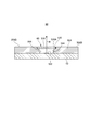
- FIG. 11 is a diagram schematically showing a cross-sectional configuration of the light emitting module 80.
- the LED chip 522 is a plate-like chip having a substantially square shape in plan view, and electrodes are formed on each of the top surface 522A and the bottom surface 522B as shown in FIG.
- a chip light emitting unit 522A1 that emits ultraviolet light H is provided on the upper surface 522A.
- the electrode on the bottom surface 522B is die-bonded to the wiring pattern 529, and the electrode on the top surface 522A is bonded to the wiring pattern 529 with a wire 537.
- the electrodes on the top surface 522A and the bottom surface 522B of the LED chip 522 are electrically connected to the wiring pattern 529.
- the LED chips 522 are arranged in a row on the mounting surface 58 of the mounting substrate 52 with a predetermined gap ⁇ (FIG. 8A).
- the size of the gap ⁇ is set to such a value that the uniformity in the longitudinal direction of the linear light source is good and a desired irradiation intensity can be obtained.
- the size of the LED chip 522 is 1.5 mm ⁇ 1.5 mm, and the gap ⁇ at this time is set to 0.1 mm to 2.0 mm. Note that the arrangement interval of the LED chips 522 can be determined by the distance between the optical axes of the adjacent LED chips 522 instead of the gap ⁇ .
- Zener diode 523 is a diode element that prevents application of overvoltage to LED chip 522. In the light emitting module 80, a Zener diode 523 is provided for each of the plurality of LED chips 522.
- the plate 524 is a member that is placed on the mounting surface 58 of the mounting substrate 52, covers the entire mounting surface 58, and protects the wiring pattern 529, the LED chip 522, and the wires 537.
- the plate 524 is formed of, for example, a resin material or a metal material (for example, an aluminum alloy) having excellent thermal conductivity. As shown in FIG. 10, the plate 524 has an emission opening 530, and the emission opening 530 is formed to have a size that exposes all the LED chips 522 arranged on the mounting substrate 52. .
- the cover member 526 is a light transmissive plate-like member that closes the emission opening 530. As shown in FIG. 9, a step portion 530A is formed on the inner periphery of the emission opening 530 over the entire circumference at a position 0.2 to 20 mm deep from the surface, and a cover member is formed on the step portion 530A. 526 is placed. A fixing material space 534 which is a recess connected to the step portion 530A is provided at both ends in the longitudinal direction of the emission opening 530, and an adhesive is injected into the fixing material space 534, and the cover member 526 is formed by the adhesive. Fixed.
- an elastic material such as a spring material or a rubber material may be fitted in the fixing material space 534 instead of the adhesive, and the cover member 526 may be fixed so as not to fall off by an elastic force.
- an elastic material for fixing the cover member 526 the elastic material and the cover member 526 can be easily detached from the plate 524, and the cover member 526 can be easily replaced.
- a reflection surface 544 is provided on the inner peripheral surface of the emission opening 530 below the step portion 530 ⁇ / b> A.
- the directivity is improved by the reflection surface 544 controlling the light distribution of the light H emitted from the LED chip 522.
- the reflection surface 544 forms a curved reflection surface that reflects the light H of the LED chip 522 substantially parallel to the optical axis of the LED chip 522, and thereby substantially parallel light is emitted from the emission opening 530. Since the reflecting surface 544 collimates the light H, the amount of light shielded by the emission opening 530 is suppressed, and the light use efficiency is improved.
- the reflecting surface 544 is formed by a light reflecting film by vapor deposition of a reflecting material such as aluminum, a mirror finish on the inner peripheral surface, or pasting of a reflecting plate such as an aluminum plate.
- FIG. 12 is a diagram schematically showing the electrical configuration of the light emitting module 80.
- the light emitting module 80 includes N (where N ⁇ 2) LED groups G in which M (where M ⁇ 2) LED chips 522 are electrically connected in parallel. Group G is electrically connected in series. These M ⁇ N LED chips 522 are arranged in a row with a certain gap ⁇ (that is, at regular intervals) on the mounting surface 58 of the mounting substrate 52 as described above. Further, one Zener diode 523 is electrically connected in antiparallel to each LED chip 522 of the LED group G for each LED group G, and protects these LED chips 522 from overvoltage.
- a total of 48 LED chips 522 are arranged in a straight line.
- the values of M and N can be determined according to the current value and the voltage value that can be applied to the mounting substrate 52.
- FIG. 13 is a diagram showing a configuration of the mounting surface 58 of the mounting substrate 52
- FIG. 14 is an enlarged view of a portion X in FIG.
- a circuit symbol is drawn in the LED chip 522 to show the electrical connection of the LED chip 522.
- the wiring pattern 529 includes a first connection wiring portion 531 and a second connection wiring portion 532 that are continuous with each of the pair of wiring connection portions 508 and 508, and each LED group G of the LED chip 522. And a serial connection wiring portion 533 connected in series.
- the pair of wiring connection parts 508 and 508 are connected to the positive and negative wirings 512 and 512, respectively, and the first connection wiring part 531 and the second connection wiring part 532 are respectively positive and negative. Maintained at the pole potential.
- the plurality of LED groups G are arranged linearly along the longitudinal direction of the mounting substrate 52, one of the LED groups G at both ends thereof is connected to the first connection wiring portion 531 and the other is the second connection wiring. Connected to the unit 532. Further, the LED groups G are electrically connected by the serial connection wiring portion 533.
- each of the first connection wiring portion 531 and the series connection wiring portion 533 includes a die bonding portion 535, and each die group 535 includes each LED group G.
- the LED chip 522 is die-bonded.
- the second connection wiring portion 532 has a wire bonding portion 536, and the upper surface 522 A of each LED chip 522 of one LED group G is bonded to the wire bonding portion 536 with a wire 537.
- the series connection wiring part 533 has an extending part 538 extending over two adjacent LED groups G, and the die bonding part 535 and the wire bonding part 536 are provided at both ends of the extending part 538, respectively. Yes.
- each LED chip 522 is connected to the wire bonding portion 536 through two wires 537.
- the number of wires 537 connecting the LED chip 522 and the wire bonding portion 536 is arbitrary.
- the wire connection portions 537A of the plurality of wires 537 are collectively provided in the vicinity of the edge portion 522C.
- the LED chip 522 is arranged in a state where the wire connection portion 537A faces the wire bonding portion 536 (that is, a state where the distance between the wire connection portion 537A and the wire bonding portion 536 is shortest).
- each of the serial connection wiring portions 533 is disposed at a position inverted for each of two adjacent LED groups G, and each LED group G is electrically connected in series. Yes.
- the adjacent LED groups G are electrically connected by the serial connection wiring part 533 extending along these, and the pattern of the serial connection wiring part 533 is formed between the LED groups G. I will not pass. Therefore, the gap between the LED groups G can also be made equal to the gap ⁇ between the LED chips 522, so that there is no illuminance unevenness due to the mismatch between the gap between the LED groups G and the gap ⁇ between the LED chips 522. The uniformity can be improved.
- a recessed portion 539 is formed in the extending portion 538 of the serial connection wiring portion 533.
- a die bonding portion 535 of the series connection wiring portion 533 facing each other is formed, and the Zener diode 523 is mounted in the recess 539.
- the Zener diode 523 is arranged at a position where the Zener diode 523 enters the recess 539 of the extending part 538 of the series connection wiring part 533, the Zener diode 523 is arranged between the LED groups G. In comparison, the gaps ⁇ of all the LED chips 522 are aligned, and the Zener diode 523 does not cause uneven illumination. Further, since the Zener diode 523 is disposed near the wire bonding portion 536, the wire 537 is not lengthened.
- the plate 524 of the light emitting module 80 is provided with a plurality (at least two or more) of protrusions 540 on the surface (bottom surface) that covers the mounting substrate 52, and the mounting surface of the mounting substrate 52. 58 is also provided with a hole 542 for receiving the protrusion 540. Since the plate 524 is positioned with respect to the mounting substrate 52 by the engagement of the protrusions 540 and the hole 542, the inner peripheral surface of the emission opening 530 of the plate 524 becomes the wire 537 or the LED chip due to misalignment of the plate 524, There is no such thing as touching 522 and damaging it.
- the cover member 526 is provided in the exit opening 530 of the plate 524 as described above, the LED chip 522 and the wire 537 exposed from the exit opening 530 are protected by the cover member 526, and these damages are surely made. To be prevented.
- each of the second reflecting surfaces 57 is located closer to the predetermined irradiation position T than the first reflecting surface 55, and the light emitting unit 60 at the opposite position is connected to the other light emitting unit 60.
- the first reflective surface 55 is spaced apart from the first reflective surface 55, and a space Q is disposed between the first reflective surface 55 and the first reflective surface 55. Then, the ultraviolet rays Ib incident on the second reflecting surface 57 at the opposite position from each of the light emitting units 60 are incident on the second reflecting surface 57 through the space Q.
- variety of the irradiation unit 30 (mounting board 52 The distance in the separating direction) is narrowed, and the ultraviolet irradiation device 1 can be made compact.
- the ultraviolet rays of each of the pair of light emitting units 60 are irradiated to the predetermined irradiation position T, the peak illuminance at the predetermined irradiation position T is increased as compared with the configuration in which the light emitting unit 60 is one.
- the pair of second reflecting surfaces 57 are spaced apart according to the separation distance L of the pair of mounting substrates 52. Thereby, also in the structure which spaces apart the 2nd reflective surface 57 from the 1st reflective surface 55, the increase in the width
- the mounting substrates 52 of the pair of light emitting modules 80 are arranged in parallel to each other. Can be suppressed.
- the irradiation unit 30 of the present embodiment all the light in the range of the emission angle ⁇ of the light emitting unit 60 is incident on one of the first reflecting surface 55 and the second reflecting surface 57 and is subjected to light distribution control. Even if the first reflecting surface 55 and the second reflecting surface 57 are separated from each other, the light utilization efficiency does not decrease.
- a plurality of ultraviolet LEDs are arranged in a row in the light emitting unit 60, and irradiates light linearly toward a predetermined irradiation position T.
- the irradiation unit 30 suitable for using the photocuring treatment of the ink by irradiating the printing surface W having a width with linear ultraviolet rays extending in the width direction is obtained.
- the first reflection surface 55 and the second reflection surface 57 are both elliptical reflection surfaces that condense the ultraviolet rays of the light emitting unit 60 at the opposite position to the predetermined irradiation position T.
- a high peak illuminance is obtained at T.
- the ultraviolet irradiation device 1 of the present embodiment blows cooling air to each of the irradiation units 30 and air-cools, the output of the ultraviolet LED provided in the light emitting unit 60 of each irradiation unit 30 can be increased.
- the ultraviolet irradiation device 1 includes a hollow tubular support column 36 that extends over each of the irradiation units 30 and into which outside air is introduced. It is provided for each. Thereby, each of the irradiation unit 30 can be cooled individually with cooling air.
- each of the irradiation units 30 includes a base body 50 to which the light emitting module 80 is attached, and the base body 50 is an integrally molded product including heat radiating fins 42 to which cooling air is blown. .
- the thermal resistance between the light emitting module 80 and the radiation fin 42 is suppressed, and heat dissipation is improved.
- each of the radiating fins 42 is provided in parallel with the cooling air blowing direction B, mixing of the cooling air blown out from each blowing hole 40 is suppressed, and irradiation is performed.
- the thermal independence of the cooling air for each unit 30 is enhanced.
- the wire connection portion 537A of the LED chip 522 is inverted for each LED group G, and each of the series connection wiring portions 533 is inverted for every two adjacent LED groups G. Is arranged.
- the adjacent LED groups G are electrically connected by the serial connection wiring portion 533 extending along the LED groups G, so that the pattern of the serial connection wiring portion 533 may pass through the gap between the LED groups G. Absent. Therefore, the gap between the LED groups G can also be made equal to the gap ⁇ between the LED chips 522, and uneven illuminance due to the mismatch between the gap between the LED groups G and the gap ⁇ between the LED chips 522 occurs.
- more LED chips 522 can be arranged with high density. As a result, the light emitting module 80 having a small size and high output and good uniformity can be obtained. Furthermore, the LED chip 522 and the wire 537 are protected by the plate 524, and these damages can be prevented.
- a recess 539 is formed between the die bonding portion 535 and the wire bonding portion 536 of the series connection wiring portion 533, and the Zener diode 523 is disposed in the recess 539. Accordingly, since the Zener diodes 523 are arranged at the positions where they enter the series connection wiring portion 533, the gaps ⁇ of all the LED chips 522 are smaller than when the Zener diodes 523 are arranged between the LED groups G. Thus, the Zener diode 523 does not cause illuminance unevenness. Further, since the Zener diode 523 is disposed near the wire bonding portion 536, the wire 537 is not lengthened.
- the mounting substrate 52 is provided with a hole 542 as a positioning portion that engages and positions the protrusion 540 of the plate 524. Since the plate 524 is positioned with respect to the mounting substrate 52 by the engagement of the protrusions 540 and the hole 542, the inner peripheral surface of the emission opening 530 of the plate 524 becomes the wire 537 or the LED chip due to misalignment of the plate 524, There is no such thing as touching and damaging 522 or the like.
- the mounting board 52 is provided with the hole 542 and the plate 524 is provided with the protrusion 540. On the contrary, the mounting board 52 is provided with a protrusion and the hole engaging with the protrusion is provided. It may be provided on the plate 524.
- the cover member 526 is provided in the emission opening 530 of the plate 524, the LED chip 522 and the wire 537 can be reliably protected and the damage can be prevented.
- the reflection surface 544 for collimating the light H of the LED chip 522 is provided on the inner peripheral surface of the emission opening 530 of the plate 524, the amount of light shielded by the inner peripheral surface is suppressed. , Light utilization efficiency can be improved.
- the first reflection surface 55 and the second reflection surface 57 of the irradiation unit 30 are both elliptical reflection surfaces that collect the light of the light emitting unit 60 at the opposite position at the predetermined irradiation position T. Illustrated. However, the present invention is not limited to this, and the second reflecting surface 57 may be a flat surface or a curved surface different from the first reflecting surface 55. Further, the condensing position of the first reflecting surface 55 may be different from the predetermined irradiation position T.
- FIG. 15 is a diagram showing a configuration of an irradiation unit 130 according to this modification.
- the irradiation unit 130 emits ultraviolet rays having a predetermined width R around the unit optical axis K in a linear shape.
- the first reflecting surface 155 is formed on an elliptical reflecting surface having the light emitting unit 60 as the first focal point f1 and the second focal point f2 inside the irradiation unit 130, and the ultraviolet ray Ia of the light emitting unit 60 is emitted from the first reflecting surface 155.
- the predetermined irradiation position T To the predetermined irradiation position T, the light is spread in the width direction (the direction in which the pair of mounting substrates 52 are separated) and emitted.
- the second reflecting surface 157 is a planar reflecting surface, and the second reflecting surface 157 also emits the ultraviolet rays Ib of the light emitting unit 60 in the width direction toward the predetermined irradiation position T.
- the predetermined irradiation position T is linearly irradiated with the ultraviolet rays spread in the predetermined width R in the width direction.
- the lower end portion 155A of the first reflecting surface 155 and the upper end portion 157A of the second reflecting surface 157 are located on the straight line E2 that divides the radiation range of the light emitting unit 60, and the radiation angle ⁇ is All ultraviolet rays are incident on either the first reflecting surface 155 or the second reflecting surface 157.
- the second reflecting surface 157 may be a curved surface such as a paraboloid.
- FIG. 16 is a diagram showing a configuration of an irradiation unit 230 according to this modification.
- the radiation fins 242 of the irradiation unit 230 may extend in the longitudinal direction A, and each radiation fin 242 may be exposed to cooling air flowing in the longitudinal direction A of the housing 2.
- the heat radiating fin unit 243 in which the heat radiating fins 242 are integrally formed is formed separately from the base body 250.
- FIG. 17 is a diagram showing a configuration of an irradiation unit 330 according to this modification.
- the irradiation unit 330 may be provided with a plurality of cooling pipes 370 through which a refrigerant such as cooling water circulates instead of the heat radiating fins, and may be cooled by the refrigerant.
- the base body 350 includes a separable part 351 on the back side of the mounting substrate 52, and the cooling pipe 370 is sandwiched between the part 351 and the base body 350, and is accommodated in the base body 350. .
- the refrigerant in the cooling pipe 370 flows near the mounting substrate 52, so that the heat of the light emitting unit 60 of the mounting substrate 52 is efficiently recovered into the refrigerant.
- the light emitting module 80 in which the cover member 526 is fixed to the plate 524 with an adhesive is illustrated, but the present invention is not limited thereto. That is, as in the light emitting module 680 shown in FIG. 18, a leaf spring that holds and holds the cover member 526 with a spring force is attached to the emission opening 530 as the holding member 550, and the cover member 526 is fixed by the holding member 550. Also good. According to this configuration, since the cover member 526 is only held by the spring force of the holding member 550, the cover member 526 can be easily removed. Instead of the leaf spring, an elastic member such as rubber that holds the cover member 526 with an elastic force may be used for the holding member 550.
- an elastic member such as rubber that holds the cover member 526 with an elastic force may be used for the holding member 550.
- the cover member 526 may include a lens unit 555 that controls the distribution of transmitted light.
- the lens unit 555 for example, a cylindrical lens that is long in the arrangement direction of the LED chips 522 is preferably used. In this case, by holding the cover member 526 with the holding member 550, the cover member 526 can be easily replaced with one that can obtain a desired light distribution.
- the configuration in which one row of LED chips 522 is mounted on the mounting substrate 52 is illustrated, but the present invention is not limited thereto.
- a plurality of lines Ln of the LED chips 522 arranged in a row can be mounted in parallel as in the mounting substrate 620 shown in FIG.
- the first connection wiring portion 531, the second connection wiring portion 532, and the series connection wiring portion 533 are provided for each line Ln.
- the plate 524 is provided with one emission opening 530 having a size that exposes the LED chips 522 of all these lines Ln or individual emission openings 530 for each row of the LED chips 522.
- the light emitting unit 60 is not limited to the LED chip 522 of the ultraviolet LED, and can be configured by any light emitting element.
- the ultraviolet irradiation device 1 can be used by being incorporated in an arbitrary apparatus such as a film manufacturing apparatus in addition to the printing apparatus.
- UV irradiation device irradiation device
- Housing Intake fan 8
- Exhaust fan 30 Exhaust fan 30, 130, 230, 330
- Irradiation unit 32
- Mounting member 36
- Post (tube) 39
- Ventilation space 40
- Blowout holes 42
- Base body 52
- Mounting substrate 54
- First reflector 55
- 155 First reflecting surface 56
- Mounting surface 60
- Light emitting portion 80
- Light Emitting Module 243 Radiation Fin Unit 370
- Cooling Tube 522
- LED Chip (Light Emitting Element) 522B
- Zener diode (diode element) 524
- Plate 526 Cover member 529
- Wiring pattern 530
- Outgoing opening 530A
- Series connection wiring portion 535
- Die bonding portion (first bonding portion)
Landscapes
- Engineering & Computer Science (AREA)
- General Engineering & Computer Science (AREA)
- Led Device Packages (AREA)
- Non-Portable Lighting Devices Or Systems Thereof (AREA)
Abstract
La présente invention améliore l'éclairement de crête et permet une économie d'espace. Une unité d'irradiation (30) qui applique de la lumière à une position d'irradiation prédéterminée (T) comporte : une paire de substrats de montage (52) qui ont des parties électroluminescentes (60) comprenant des DEL ultraviolettes, respectivement et qui est disposée de telle sorte que les parties électroluminescentes (60) s'opposent l'une à l'autre; et une paire de premières surfaces de réflexion (55) et une paire de secondes surfaces de réflexion (57) qui sont disposées à des positions opposées de telle sorte que les premières surfaces de réflexion appariées (55) s'opposent aux parties électroluminescentes (60) des substrats de montage (52), respectivement, et les secondes surfaces de réflexion appariées (57) s'opposent aux parties électroluminescentes (60) des substrats de montage (52), respectivement, et qui réalisent une commande de distribution de lumière de la lumière des parties électroluminescentes (60) positionnées à des positions opposées. Les secondes surfaces de réflexion (57) sont situées plus près de la position d'irradiation prédéterminée (T) que les premières surfaces de réflexion (55), et sont chacune espacées de la partie électroluminescente (60) à sa position opposée, par rapport aux premières surfaces de réflexion (55), de façon à être disposées sur l'autre côté de la partie électroluminescente (60). Chaque seconde surface de réflexion (57) est dotée d'un espace (Q) se trouvant entre la seconde surface de réflexion (57) et une surface correspondante parmi les premières surfaces de réflexion (55). La lumière, qui entre dans chaque seconde surface de réflexion (57) de la partie électroluminescente (60) à sa position opposée, entre dans la seconde surface de réflexion (57) à travers l'espace (Q).
Applications Claiming Priority (2)
| Application Number | Priority Date | Filing Date | Title |
|---|---|---|---|
| JP2017-063474 | 2017-03-28 | ||
| JP2017063474A JP6787219B2 (ja) | 2017-03-28 | 2017-03-28 | 照射ユニット、及び照射装置 |
Publications (1)
| Publication Number | Publication Date |
|---|---|
| WO2018180902A1 true WO2018180902A1 (fr) | 2018-10-04 |
Family
ID=63677914
Family Applications (1)
| Application Number | Title | Priority Date | Filing Date |
|---|---|---|---|
| PCT/JP2018/011455 Ceased WO2018180902A1 (fr) | 2017-03-28 | 2018-03-22 | Unité d'irradiation et dispositif d'irradiation |
Country Status (3)
| Country | Link |
|---|---|
| JP (1) | JP6787219B2 (fr) |
| TW (1) | TW201903322A (fr) |
| WO (1) | WO2018180902A1 (fr) |
Cited By (1)
| Publication number | Priority date | Publication date | Assignee | Title |
|---|---|---|---|---|
| JPWO2020262025A1 (fr) * | 2019-06-28 | 2020-12-30 |
Citations (8)
| Publication number | Priority date | Publication date | Assignee | Title |
|---|---|---|---|---|
| JPH0943399A (ja) * | 1995-07-31 | 1997-02-14 | Iwasaki Electric Co Ltd | 紫外線照射装置 |
| JPH1098215A (ja) * | 1996-09-24 | 1998-04-14 | Toyoda Gosei Co Ltd | 発光ダイオード装置 |
| JP2001203395A (ja) * | 2000-01-20 | 2001-07-27 | Sanyo Electric Co Ltd | 混成集積回路装置 |
| WO2005055328A1 (fr) * | 2003-12-05 | 2005-06-16 | Mitsubishi Denki Kabushiki Kaisha | Dispositif electroluminescent et instrument d'eclairage faisant appel a ce dispositif |
| JP2012221621A (ja) * | 2011-04-05 | 2012-11-12 | Harison Toshiba Lighting Corp | 光照射装置 |
| JP2012227511A (ja) * | 2011-04-20 | 2012-11-15 | Lg Innotek Co Ltd | 紫外線発光素子パッケージ |
| JP2015060745A (ja) * | 2013-09-19 | 2015-03-30 | 岩崎電気株式会社 | 光照射装置 |
| JP2015198139A (ja) * | 2014-03-31 | 2015-11-09 | Hoya Candeo Optronics株式会社 | 光照射ユニット |
-
2017
- 2017-03-28 JP JP2017063474A patent/JP6787219B2/ja active Active
-
2018
- 2018-03-22 WO PCT/JP2018/011455 patent/WO2018180902A1/fr not_active Ceased
- 2018-03-22 TW TW107109861A patent/TW201903322A/zh unknown
Patent Citations (8)
| Publication number | Priority date | Publication date | Assignee | Title |
|---|---|---|---|---|
| JPH0943399A (ja) * | 1995-07-31 | 1997-02-14 | Iwasaki Electric Co Ltd | 紫外線照射装置 |
| JPH1098215A (ja) * | 1996-09-24 | 1998-04-14 | Toyoda Gosei Co Ltd | 発光ダイオード装置 |
| JP2001203395A (ja) * | 2000-01-20 | 2001-07-27 | Sanyo Electric Co Ltd | 混成集積回路装置 |
| WO2005055328A1 (fr) * | 2003-12-05 | 2005-06-16 | Mitsubishi Denki Kabushiki Kaisha | Dispositif electroluminescent et instrument d'eclairage faisant appel a ce dispositif |
| JP2012221621A (ja) * | 2011-04-05 | 2012-11-12 | Harison Toshiba Lighting Corp | 光照射装置 |
| JP2012227511A (ja) * | 2011-04-20 | 2012-11-15 | Lg Innotek Co Ltd | 紫外線発光素子パッケージ |
| JP2015060745A (ja) * | 2013-09-19 | 2015-03-30 | 岩崎電気株式会社 | 光照射装置 |
| JP2015198139A (ja) * | 2014-03-31 | 2015-11-09 | Hoya Candeo Optronics株式会社 | 光照射ユニット |
Cited By (4)
| Publication number | Priority date | Publication date | Assignee | Title |
|---|---|---|---|---|
| JPWO2020262025A1 (fr) * | 2019-06-28 | 2020-12-30 | ||
| WO2020262025A1 (fr) * | 2019-06-28 | 2020-12-30 | 富士フイルム株式会社 | Appareil de projection |
| JP7209836B2 (ja) | 2019-06-28 | 2023-01-20 | 富士フイルム株式会社 | 投射装置 |
| US12111562B2 (en) | 2019-06-28 | 2024-10-08 | Fujifilm Corporation | Projection device |
Also Published As
| Publication number | Publication date |
|---|---|
| JP6787219B2 (ja) | 2020-11-18 |
| JP2018166082A (ja) | 2018-10-25 |
| TW201903322A (zh) | 2019-01-16 |
Similar Documents
| Publication | Publication Date | Title |
|---|---|---|
| KR101270066B1 (ko) | 자동차 헤드라이트 모듈 | |
| JP5421799B2 (ja) | Ledユニット | |
| US20110216536A1 (en) | Illumination device | |
| US8911125B2 (en) | Circuit module, light emitting module, and automotive lamp | |
| CN107199164B (zh) | 光照射装置 | |
| CN109973840B (zh) | 具有led和圆柱形透镜的发光体 | |
| US10209005B2 (en) | UV LED systems and methods | |
| JP7176211B2 (ja) | 照明装置 | |
| JP6094663B2 (ja) | 発光装置 | |
| KR101748016B1 (ko) | 반사기를 갖춘 조명 유닛 | |
| KR20170113127A (ko) | 방열 장치 및 그것을 구비하는 광 조사 장치 | |
| US11432401B2 (en) | Electronic assembly and automotive luminous device | |
| WO2018180902A1 (fr) | Unité d'irradiation et dispositif d'irradiation | |
| KR200491878Y1 (ko) | 광 조사 모듈 | |
| JP2013016681A (ja) | 放熱部材および放熱機構 | |
| KR20170113178A (ko) | 방열 장치 및 그것을 구비하는 광 조사 장치 | |
| KR20190075782A (ko) | 광 조사 장치 | |
| TW202210171A (zh) | 光照射裝置 | |
| CN113056637B (zh) | 机动车光照装置 | |
| JP2020520541A (ja) | 高い放射照度の照明アセンブリ | |
| JP2016066642A (ja) | 光源装置 | |
| ES2988255T3 (es) | Dispositivo de irradiación de luz y dispositivo de impresión | |
| KR20180073288A (ko) | 방열성이 향상된 엘이디 소자 배열용 인쇄회로기판 | |
| KR20200011678A (ko) | 자외선 광 조사 장치 | |
| JP7007569B2 (ja) | 発光装置 |
Legal Events
| Date | Code | Title | Description |
|---|---|---|---|
| 121 | Ep: the epo has been informed by wipo that ep was designated in this application |
Ref document number: 18777280 Country of ref document: EP Kind code of ref document: A1 |
|
| NENP | Non-entry into the national phase |
Ref country code: DE |
|
| 122 | Ep: pct application non-entry in european phase |
Ref document number: 18777280 Country of ref document: EP Kind code of ref document: A1 |