WO2018180902A1 - 照射ユニット、及び照射装置 - Google Patents
照射ユニット、及び照射装置 Download PDFInfo
- Publication number
- WO2018180902A1 WO2018180902A1 PCT/JP2018/011455 JP2018011455W WO2018180902A1 WO 2018180902 A1 WO2018180902 A1 WO 2018180902A1 JP 2018011455 W JP2018011455 W JP 2018011455W WO 2018180902 A1 WO2018180902 A1 WO 2018180902A1
- Authority
- WO
- WIPO (PCT)
- Prior art keywords
- light emitting
- irradiation
- light
- irradiation unit
- mounting
- Prior art date
- Legal status (The legal status is an assumption and is not a legal conclusion. Google has not performed a legal analysis and makes no representation as to the accuracy of the status listed.)
- Ceased
Links
Images


Classifications
-
- F—MECHANICAL ENGINEERING; LIGHTING; HEATING; WEAPONS; BLASTING
- F21—LIGHTING
- F21S—NON-PORTABLE LIGHTING DEVICES; SYSTEMS THEREOF; VEHICLE LIGHTING DEVICES SPECIALLY ADAPTED FOR VEHICLE EXTERIORS
- F21S2/00—Systems of lighting devices, not provided for in main groups F21S4/00 - F21S10/00 or F21S19/00, e.g. of modular construction
-
- F—MECHANICAL ENGINEERING; LIGHTING; HEATING; WEAPONS; BLASTING
- F21—LIGHTING
- F21V—FUNCTIONAL FEATURES OR DETAILS OF LIGHTING DEVICES OR SYSTEMS THEREOF; STRUCTURAL COMBINATIONS OF LIGHTING DEVICES WITH OTHER ARTICLES, NOT OTHERWISE PROVIDED FOR
- F21V29/00—Protecting lighting devices from thermal damage; Cooling or heating arrangements specially adapted for lighting devices or systems
- F21V29/50—Cooling arrangements
- F21V29/502—Cooling arrangements characterised by the adaptation for cooling of specific components
- F21V29/503—Cooling arrangements characterised by the adaptation for cooling of specific components of light sources
-
- F—MECHANICAL ENGINEERING; LIGHTING; HEATING; WEAPONS; BLASTING
- F21—LIGHTING
- F21V—FUNCTIONAL FEATURES OR DETAILS OF LIGHTING DEVICES OR SYSTEMS THEREOF; STRUCTURAL COMBINATIONS OF LIGHTING DEVICES WITH OTHER ARTICLES, NOT OTHERWISE PROVIDED FOR
- F21V29/00—Protecting lighting devices from thermal damage; Cooling or heating arrangements specially adapted for lighting devices or systems
- F21V29/50—Cooling arrangements
- F21V29/56—Cooling arrangements using liquid coolants
-
- F—MECHANICAL ENGINEERING; LIGHTING; HEATING; WEAPONS; BLASTING
- F21—LIGHTING
- F21V—FUNCTIONAL FEATURES OR DETAILS OF LIGHTING DEVICES OR SYSTEMS THEREOF; STRUCTURAL COMBINATIONS OF LIGHTING DEVICES WITH OTHER ARTICLES, NOT OTHERWISE PROVIDED FOR
- F21V29/00—Protecting lighting devices from thermal damage; Cooling or heating arrangements specially adapted for lighting devices or systems
- F21V29/50—Cooling arrangements
- F21V29/60—Cooling arrangements characterised by the use of a forced flow of gas, e.g. air
- F21V29/67—Cooling arrangements characterised by the use of a forced flow of gas, e.g. air characterised by the arrangement of fans
-
- F—MECHANICAL ENGINEERING; LIGHTING; HEATING; WEAPONS; BLASTING
- F21—LIGHTING
- F21V—FUNCTIONAL FEATURES OR DETAILS OF LIGHTING DEVICES OR SYSTEMS THEREOF; STRUCTURAL COMBINATIONS OF LIGHTING DEVICES WITH OTHER ARTICLES, NOT OTHERWISE PROVIDED FOR
- F21V29/00—Protecting lighting devices from thermal damage; Cooling or heating arrangements specially adapted for lighting devices or systems
- F21V29/50—Cooling arrangements
- F21V29/70—Cooling arrangements characterised by passive heat-dissipating elements, e.g. heat-sinks
- F21V29/74—Cooling arrangements characterised by passive heat-dissipating elements, e.g. heat-sinks with fins or blades
- F21V29/76—Cooling arrangements characterised by passive heat-dissipating elements, e.g. heat-sinks with fins or blades with essentially identical parallel planar fins or blades, e.g. with comb-like cross-section
-
- F—MECHANICAL ENGINEERING; LIGHTING; HEATING; WEAPONS; BLASTING
- F21—LIGHTING
- F21V—FUNCTIONAL FEATURES OR DETAILS OF LIGHTING DEVICES OR SYSTEMS THEREOF; STRUCTURAL COMBINATIONS OF LIGHTING DEVICES WITH OTHER ARTICLES, NOT OTHERWISE PROVIDED FOR
- F21V7/00—Reflectors for light sources
- F21V7/04—Optical design
- F21V7/08—Optical design with elliptical curvature
Definitions
- the present invention relates to an irradiation unit and an irradiation apparatus.
- a plurality of LEDs arranged in a row and a reflecting member that reflects the light of these LEDs are provided, and a plurality of light source units that emit linear light are provided.
- Each light source unit has an axis on which the linear light extends.
- an irradiation device that is arranged in a direction orthogonal to a direction and that irradiates an irradiation target object by superimposing linear lights (see, for example, Patent Document 1).
- a plurality of LEDs arranged in a line, a reflecting member that reflects the light of these LEDs toward a predetermined focal point, and a rod lens that condenses the direct light component of these LEDs at a predetermined focal point of the reflecting member;
- an irradiation apparatus that irradiates an irradiation object with linear light that is condensed at a predetermined focal point (see, for example, Patent Document 2). These irradiation apparatuses are widely used in various apparatuses such as a printing apparatus and a film manufacturing apparatus.
- the installation space of the irradiation apparatus may be narrow.
- the width dimension in the direction orthogonal to the axial direction of the linear light is not suitable for the installation space, and it may be difficult to fit the irradiation apparatus in the installation space of the installation destination apparatus. is there.
- the configuration in which the LED arrangement density is increased to increase the peak illuminance it is necessary to increase the cooling performance of the LED, which leads to an increase in the size of the irradiation device.
- An object of the present invention is to provide an irradiation unit and an irradiation apparatus that can increase peak illuminance and can save space.
- the present invention relates to an irradiation unit that irradiates light to a predetermined irradiation position, each of which has a light emitting unit including a light emitting element, and a pair of mounting substrates disposed so that the light emitting units face each other, and the mounting substrate
- a light emitting unit including a light emitting element
- a pair of mounting substrates disposed so that the light emitting units face each other, and the mounting substrate
- Each of the light emitting units, and a pair of first reflecting surfaces and a second reflecting surface for controlling the light distribution of the light emitting units at the facing positions, and each of the second reflecting surfaces.
- the first reflection surface is located closer to the predetermined irradiation position than the first reflection surface, and is spaced apart from the first reflection surface from the light emission portion at the opposite position to the other light emission portion, and the first reflection surface;
- a light is disposed between each of the light emitting units and is incident on the second reflecting surface at an opposing position, and is incident on the second reflecting surface through the space.
- the present invention is characterized in that, in the irradiation unit, the pair of second reflecting surfaces are spaced apart from each other according to the separation distance of the pair of mounting substrates.
- the present invention is characterized in that, in the irradiation unit, the pair of mounting boards are arranged in parallel to each other.
- the present invention is characterized in that, in the irradiation unit, all light in a range of a predetermined radiation angle of the light emitting unit is incident on either the first reflection surface or the second reflection surface.
- the present invention is characterized in that, in the irradiation unit, a plurality of the light emitting elements are arranged in a row in the light emitting portion, and the light is irradiated linearly toward the predetermined irradiation position.
- the present invention is characterized in that, in the irradiation unit, the first reflection surface and the second reflection surface are elliptical reflection surfaces for condensing the light of the light emitting unit at a facing position at the predetermined irradiation position. .
- the first reflection surface is an elliptical reflection surface that condenses the light emitting unit at the opposed position to the predetermined irradiation position
- the second reflection surface is a flat surface or the first reflection surface. It is characterized by a curved surface different from one reflecting surface.
- the present invention provides the irradiation unit, wherein the mounting substrate, a wiring pattern for wiring the plurality of light emitting elements arranged in a line on the mounting surface of the mounting substrate, and the mounting surface of the mounting substrate are overlapped, A plate having an emission opening surrounding the plurality of light emitting elements arranged on the substrate, and the plurality of light emitting elements are electrically connected in parallel for each predetermined number,
- the wiring pattern includes a series connection wiring portion that electrically connects light emitting element groups of the light emitting elements that are electrically connected in parallel with each other, and the series connection wiring portion includes two adjacent light emitting element groups.
- a wire bonding portion of the light emitting element is inverted for each of the light emitting element groups, and each of the series connection wiring portions is adjacent to the two light emitting elements. It is characterized by being arranged at the inverted position for each group.
- the light emitting element group includes a diode element for preventing the application of an overvoltage to each light emitting element, and the series connection wiring portion has a recess.
- the diode element is disposed in the recess.
- the present invention is characterized in that, in the irradiation unit, the mounting substrate is provided with a positioning portion that engages and positions the plate.
- the present invention is characterized in that the irradiation unit includes a light-transmitting cover member that closes the exit opening.
- the present invention is characterized in that the irradiation unit includes a holding member that holds the cover member with an elastic force at an emission opening of the plate.
- the present invention is characterized in that, in the irradiation unit, a reflection surface for collimating the light of the light emitting element is provided on the inner peripheral surface of the emission opening of the plate.
- the present invention is characterized in that, in the irradiation unit, the cover member includes a lens unit for controlling transmitted light.
- the present invention includes a plurality of irradiation units according to any one of the above, and a cooling unit that cools each of the irradiation units, each of the irradiation units is connected and the cooling unit includes the irradiation unit.
- an irradiation apparatus characterized in that cooling air is blown to each of the units to cool the air, or cooling is performed through each of the irradiation units.
- the cooling unit in the irradiation apparatus, includes a tube body that extends over each of the irradiation units and into which the outside air is introduced, and a blowing hole that blows the outside air is provided on the tube body. It is provided for each unit.
- each of the irradiation units includes a base body to which the mounting substrate is attached, and the base body is an integrally molded product including a radiation fin to which the cooling air is blown. It is characterized by.
- the present invention is characterized in that, in the irradiation apparatus, the heat dissipating fins are provided in parallel to the cooling air blowing direction.
- peak illuminance can be increased and space saving can be achieved.
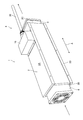
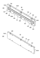
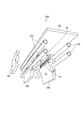
- FIG. 1 is a side view showing a configuration of an ultraviolet irradiation apparatus according to an embodiment of the present invention.
- FIG. 2 is an exploded perspective view of the ultraviolet irradiation device.
- FIG. 3 is a diagram showing an internal configuration of the ultraviolet irradiation device.
- FIG. 4 is a perspective view showing the configuration of the irradiation unit.
- FIG. 5 is a schematic view of the irradiation unit as seen from the fan mounting direction of the housing.
- FIG. 6 is an explanatory diagram of light distribution control of the irradiation unit.
- 7A and 7B are perspective views of the light emitting module, where FIG. 7A is a perspective view of the front surface, and FIG. 7B is a perspective view of the back surface.
- FIG. 8A and 8B are diagrams illustrating a configuration of the light emitting module, where FIG. 8A is a plan view, FIG. 8B is a front view, FIG. 8C is a bottom view, and FIG. FIG. 9 is a cross-sectional view taken along the line IX-IX in FIG.
- FIG. 10 is an exploded perspective view of the light emitting module.
- FIG. 11 is a diagram schematically showing a cross-sectional configuration of the light emitting module.
- FIG. 12 is a diagram schematically illustrating an electrical configuration of the light emitting module.
- FIG. 13 is a diagram illustrating a wiring pattern of the light emitting module.
- FIG. 14 is an enlarged view of a portion X in FIG. FIG.
- FIG. 15 is a diagram showing a configuration of an irradiation unit according to the first modification of the present invention.
- FIG. 16 is a diagram showing a configuration of an irradiation unit according to the second modification of the present invention.
- FIG. 17 is a diagram showing a configuration of an irradiation unit according to the third modification of the present invention.
- FIG. 18 is a diagram showing a configuration of a light emitting module according to a fourth modification of the present invention.
- FIG. 19 is a cross-sectional view showing a configuration of a light emitting module according to a fifth modification of the present invention.
- FIG. 20 is a diagram showing the configuration of the mounting surface of the mounting board according to the sixth modification of the present invention.
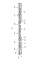
- FIG. 1 is a side view showing a configuration of an ultraviolet irradiation device 1 according to the present embodiment.
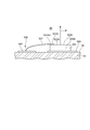
- the ultraviolet irradiation device 1 is incorporated as an inter-deck UV drying device in a built-in space provided in an offset printing device using ultraviolet curable ink, and ultraviolet curable ink applied to the printing surface W (FIG. 5) of the printed matter is ultraviolet-rayed. Cure by irradiation.
- the ultraviolet irradiation device 1 of this embodiment includes a housing 2, a power supply mechanism 4, an intake fan 6, and an exhaust fan 8.
- the housing 2 is a rectangular parallelepiped case extending in the width direction of the printed material (direction perpendicular to the transport direction), and is disposed in the offset printing apparatus with the bottom surface 2D facing the printed surface of the printed material.
- the power supply mechanism 4 is a mechanism for supplying external power to the housing 2, and is provided on the top surface 2 ⁇ / b> A of the housing 2.
- the intake fan 6 and the exhaust fan 8 are air blowing means for flowing cooling air into the housing 2.
- the intake fan 6 is provided on one side surface 2B of the housing 2, and the exhaust fan 8 is provided on the other side surface 2C. Is provided. By operating the intake fan 6 and the exhaust fan 8, cooling air flows in the longitudinal direction A of the housing 2, and the inside of the housing 2 is air-cooled.
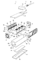
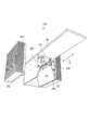
- FIG. 2 is an exploded perspective view of the ultraviolet irradiation device 1.
- the housing 2 includes a case main body 10, a top plate 12, and a bottom plate 14.
- the case main body 10 is a rectangular parallelepiped box that is open on the top surface side, and fan mounting holes 15 are formed on the side surfaces 2C and 2B on both sides.
- An exhaust fan 8 is attached.
- the top plate 12 is a member that closes the top side of the case body 10, and the top plate 12 has a mounting opening 16 to which the power supply mechanism 4 is attached.
- the power supply mechanism 4 includes a mounting box 18 attached to the mounting opening 16 and a power supply cable 20 connected to the mounting box 18 and transmitting external power.
- the bottom plate 14 is a member attached to the bottom surface 10D of the case body 10.
- An exit opening 22 is formed in the bottom plate 14 at a position corresponding to the light passage hole 17 opened in the bottom surface 10 ⁇ / b> D of the case body 10.
- the light passage hole 17 and the emission opening 22 are formed in a rectangular shape that is long in the longitudinal direction A of the housing 2, and linear ultraviolet rays extending in the longitudinal direction A (FIG. 1) are transmitted through the light passage hole 17, and The light is emitted through the emission opening 22.
- a quartz cover glass 24 that closes the light passage hole 17 and the emission opening 22 is provided between the case body 10 and the bottom plate 14.
- FIG. 3 is a diagram showing an internal configuration of the ultraviolet irradiation device 1.
- a plurality of (three in the illustrated example) irradiation units 30 and mounting members 32 to which these irradiation units 30 are attached are housed in the housing 2.
- the attachment member 32 is a member that holds each of the irradiation units 30 in a connected state in the longitudinal direction A of the housing 2.
- the mounting member 32 includes a pair of side plates 34B and 34C that are disposed facing the side surfaces 2B and 2C of the housing 2, a pair of support columns 36 and 36 that extend between the side plates 34B and 34C, and a mounting plate. 62, and the irradiation unit 30 is fixed to the mounting plate 62.
- the mounting member 32 includes the support columns 36 and 36 as cooling means for guiding cooling air to each irradiation unit 30 and cooling it by air.
- the columns 36 and 36 are hollow tubes that are disposed on the bottom surface side of the irradiation unit 30 and extend over each of the irradiation units 30, and the side plate 34 ⁇ / b> B to which the columns 36 and 36 are connected.
- the support columns 36 and 36 are formed with a large number of blow holes 40 on the surface 36A facing the irradiation unit 30, and the cooling air introduced from the inlet 38 enters the irradiation unit 30 facing the facing surface 36A. It blows out from the blowing hole 40 toward, and each irradiation unit 30 is air-cooled with cooling air.
- each irradiation unit 30 is provided with a large number of rectangular fin-shaped radiation fins 42 disposed at the respective positions of the blowout holes 40.
- the blown cooling air is blown out.
- each irradiation unit 30 is efficiently cooled by the cooling air thermally independent from each other.
- each plate surface 42B of the radiation fin 42 is provided in parallel with the blowing direction B of the cooling air (the direction from the bottom surface 2D of the housing 2 toward the top surface 2A). Mixing of the cooling air blown out from the holes 40 is suppressed until the cooling fins 42 are removed. Thereby, the thermal independence of the cooling air for each irradiation unit 30 is enhanced.
- the inside of the housing 2 is partitioned by the side plate 34 ⁇ / b> B on the side of the intake fan 6, so that almost all of the outside air taken in by the intake fan 6 is introduced into the columns 36 and 36. It has become.
- the ends of the support columns 36, 36 on the exhaust fan 8 side are closed by the side plate 34C, and all the cooling air introduced from the introduction port 38 is blown out from the blowing hole 40 and used for air cooling of the irradiation unit 30.
- the balance of the rotational speeds (intake capacity and exhaust capacity) of the intake fan 6 and the exhaust fan 8 is adjusted so that the air volume from the blowout holes 40 of the support columns 36 and 36 is substantially uniform. Thereby, each irradiation unit 30 will be air-cooled by the cooling air which became thermally independent mutually, and also by the substantially equal air volume.
- a ventilation space 39 is provided on the side of the top surface 2 ⁇ / b> A so as to extend substantially in the center in the longitudinal direction A and reach the exhaust fan 8. Cooling air blown out in the blowing direction B from each blowing hole 40 reaches the ventilation space 39 through between the radiation fins 42, flows through the ventilation space 39, and is quickly exhausted to the outside from the exhaust fan 8.
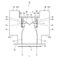
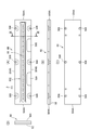
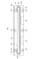
- FIG. 4 is a perspective view showing the configuration of the irradiation unit 30, and FIG. 5 is a schematic view of the irradiation unit 30 as viewed from the fan mounting direction of the housing 2.
- the irradiation unit 30 includes a pair of base bodies 50, a pair of light emitting modules 80 having a light emitting unit 60 and a mounting substrate 52, and a pair of first units facing the light emitting unit 60.
- the irradiation unit 30 is provided with a second reflecting surface 57 (described later) facing the light emitting unit 60 on each of the pair of base bodies 50. Then, each ultraviolet ray of the light emitting unit 60 is subjected to light distribution control by the first reflecting surface 55 and the second reflecting surface 57 at the opposing positions, and the unit optical axis toward the predetermined irradiation position T on the unit optical axis K. Irradiated in a line extending in a direction perpendicular to K.
- each of the plurality of irradiation units 30 is attached to the mounting member 32 and connected, and the irradiation light of each irradiation unit 30 is connected linearly on the printing surface W.
- the printing surface W is irradiated with linear ultraviolet rays having a desired length (in this embodiment, a length that crosses the printing surface W).
- each of the pair of base bodies 50 includes a board attachment surface 56 that is an attachment part of the mounting board 52 of the light emitting module 80, and as shown in FIG. 5.
- the second reflection surface 57 that is a reflection portion and the above-described many heat radiation fins 42 that are heat dissipation portions are provided.
- the substrate mounting surface 56 is a flat portion parallel to the substantially rectangular optical axis K extending in the longitudinal direction A of the housing 2, and the mounting substrate 52 is mounted substantially parallel to the substrate mounting surface 56.
- the mounting substrate 52 is a long rectangular substrate, and a light emitting unit 60 is provided on the mounting surface 58 as shown in FIG.
- the light emitting unit 60 has a number of LED chips 522 (FIG. 10) of ultraviolet LEDs arranged in a line along the direction in which the mounting substrate 52 extends, and emits ultraviolet rays linearly by the light emission of each LED chip 522. .
- the light emitting unit optical axis P which is the optical axis of the light emitting unit 60, is substantially perpendicular to the mounting surface 58 as shown in FIG.
- the pair of mounting boards 52 are arranged so that the light emitting parts 60 face each other with the unit optical axis K interposed therebetween, and the mounting surfaces 58 of the mounting boards 52 are arranged in parallel. They are perpendicular to the optical axis K and are located on the same axis E1.
- the second reflecting surface 57 is a reflecting surface extending along the extending direction of the light emitting unit 60 (longitudinal direction A of the housing 2), and is more than the light emitting unit 60 and the first reflecting surface 55 of the mounting substrate 52.
- Light distribution control is performed on the ultraviolet rays that are provided near the predetermined irradiation position T and emitted from the light emitting unit 60 at the opposite position.
- the radiation fins 42 are provided on the back side of the board mounting surface 56 in the longitudinal direction A, and radiate heat transferred from the mounting board 52 to the board mounting surface 56.
- Each of the radiation fins 42 has a substantially rectangular shape in which the lower end portion 42A extends to the back side of the second reflection surface 57, and also dissipates heat given to the second reflection surface 57 by ultraviolet irradiation.
- the base body 50 is made of a highly thermally conductive material such as aluminum, and is an integrally molded product having the above-described substrate mounting surface 56, second reflecting surface 57, and a large number of heat radiation fins 42. Thereby, compared with the case where the radiation fin 42 is formed by another member, for example, the thermal resistance between the board mounting surface 56 and the second reflection surface 57 and the radiation fin 42 can be suppressed, so that high heat radiation performance can be obtained. ing.
- the upper end portions 42C of the respective radiation fins 42 protrude from the board mounting surface 56 toward the top surface 2A of the housing 2.
- the ventilation space 39 inside the housing 2 is formed between the upper end portions 42 ⁇ / b> C of the radiation fins 42 of the pair of base bodies 50.
- the first reflector 54 is a reflector that is provided between the pair of mounting substrates 52, extends in the longitudinal direction A of the housing 2, and is convex toward the predetermined irradiation position T.
- the mounting plate 62 is a rectangular plate member that is disposed in the ventilation space 39 between the pair of base bodies 50 and extends in the longitudinal direction A of the housing 2, and as shown in FIG. 2, the side plate of the mounting member 32. It is supported by 34B and 34C.
- the mounting plate 62 is provided with a terminal block 64 for each irradiation unit 30 on the surface opposite to the surface on which the first reflector 54 is mounted. Connected.
- the mounting plate 62 may be held by the pair of base bodies 50 instead of the mounting member 32.
- each of the first reflecting surfaces 55 is a reflecting surface extending along the extending direction of the light emitting unit 60 (the longitudinal direction A), and controls the light distribution of ultraviolet rays emitted from the light emitting unit 60 at the opposite position.
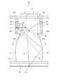
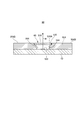
- FIG. 6 is an explanatory diagram of the light distribution control of the irradiation unit 30.
- the light emitting unit 60 of the light emitting module 80 has a predetermined radiation angle ⁇ centered on the light emitting unit optical axis P, and the irradiation unit 30 has substantially all the radiation angles ⁇ within the range.
- Ultraviolet rays are subjected to light distribution control by the first reflecting surface 55 and the second reflecting surface 57 at the position facing the light emitting unit 60. Specifically, the ultraviolet rays in the first range ⁇ 1 of the radiation angle ⁇ are incident on the first reflecting surface 55 and light distribution is controlled, and the remaining ultraviolet rays in the second range ⁇ 2 are incident on the second reflecting surface 57. Light distribution is controlled.
- the lower end portion 55A of the first reflecting surface 55 and the upper end portion 57A of the second reflecting surface 57 are positioned on a straight line E2 that divides the first range ⁇ 1 and the second range ⁇ 2. All the ultraviolet rays having the radiation angle ⁇ are incident on one of the first reflecting surface 55 and the second reflecting surface 57.
- the first reflecting surface 55 and the second reflecting surface 57 at the opposing positions of one mounting substrate 52 are not physically continuous, and as shown in FIG.
- the second reflecting surface 57 located near the predetermined irradiation position T with respect to 55 is arranged at a distance S from the first reflecting surface 55 toward the light emitting unit 60 side of the other mounting substrate 52. Yes. With the separation of the distance S, a space Q is opened between the first reflecting surface 55 and the second reflecting surface 57.
- the ultraviolet rays in the second range ⁇ 2 radiated from the respective mounting substrates 52 are not shielded by the second reflecting surface 57 disposed on the same side as the mounting substrate 52, and the space Q is not blocked. Then, the light is incident on the second reflecting surface 57 at the position facing the mounting substrate 52, and the light distribution is controlled.
- each of the pair of second reflecting surfaces 57 is thus spaced apart from the first reflecting surface 55 with the space Q therebetween, so the first reflecting surface 55 and the second reflecting surface 57 are separated.
- the width of the irradiation unit 30 is narrower than the configuration in which is a continuous reflecting surface.
- the first reflecting surface 55 and the second reflecting surface 57 are one continuous reflecting surface
- the first reflecting surface 55 of each of the first reflectors 54 is determined by the amount corresponding to the second reflecting surface 57. It extends to the irradiation position T side, and the width of the first reflector 54 is increased accordingly.
- the width of the first reflector 54 is suppressed by the amount corresponding to the second reflecting surface 57, so that the width of the irradiation unit 30 is reduced.
- each of the pair of second reflecting surfaces 57 is spaced apart from the pair of mounting boards 52 by a distance substantially equal to the distance L.
- the width of the irradiation unit 30 is narrower than that in which both the mounting substrates 52 are inclined.
- the first reflection surface 55 and the second reflection surface 57 are configured as a condensing reflection surface that condenses the ultraviolet rays of the light emitting unit 60 at the opposed positions at a predetermined irradiation position T. ing.
- the first reflection surface 55 and the second reflection surface 57 are formed on elliptical reflection surfaces in which the first focal point f1 is set to the light emitting unit 60 and the second focal point f2 is set to the predetermined irradiation position T. ing.
- the ultraviolet rays Ia and Ib incident and reflected on each of the first reflecting surface 55 and the second reflecting surface 57 are collected at a predetermined irradiation position T which is the second focal point f2. To be lighted.
- the ultraviolet rays of the light emitting units 60 of the pair of mounting substrates 52 are superimposed on the predetermined irradiation position T, the amount of light at the predetermined irradiation position T is doubled as compared with the case of one light emitting unit 60. Can be made.
- the light emitting module 80 is smaller and has higher output than the conventional light emitting modules disclosed in, for example, Japanese Patent Application Laid-Open Nos. 2006-261375 and 2013-232458, and can maintain good uniformity. It is like that.
- FIG. 7 is a perspective view of the light emitting module 80
- FIG. 7A is a perspective view seen from the front surface
- FIG. 7B is a perspective view seen from the back surface.
- 8A and 8B are diagrams illustrating a configuration of the light-emitting module 80.
- FIG. 8A is a plan view
- FIG. 8B is a front view
- FIG. 8C is a bottom view
- FIG. 8D is a side view. is there.
- FIG. 9 is a cross-sectional view taken along line IX-IX in FIG.
- the light emitting module 80 has a substantially rectangular plate shape, and a light emitting portion 502 is provided on the surface thereof.
- the light emitting unit 502 emits linear light that is elongated in the longitudinal direction of the light emitting module 80 (the direction connecting both ends 504A).
- a plurality of screw holes 506 are provided in the long side edges 504B and 504B of the light emitting module 80, and the screws are inserted into the respective screw holes 506 so that the light emitting module 80 is attached to the substrate mounting surface 56 of the irradiation unit 30. Fixed with screws.
- a pair of wiring connection portions 508 and 508 are provided on the surface of the light emitting module 80. These wiring connection portions 508 and 508 are terminals to which electrical wiring is connected, and positive and negative wirings 512 and 512 (FIG. 10) that transmit power are connected to each of the terminals.
- the pair of wiring connection portions 508 and 508 are provided on the side of one of the edge portions 504B and 504B of the light emitting module 80 (the lower side in FIG. 7A). It is arranged only in. As a result, when the two light emitting modules 80 are arranged side by side, the wiring 512, 512 may be disposed so as not to block the emitted light across the light emitting portions 502 of the two light emitting modules 80.
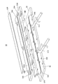
- FIG. 10 is an exploded perspective view of the light emitting module 80.
- the light emitting module 80 includes the mounting board 52 described above, a large number of LED chips 522, a Zener diode 523, a plate 524, and a cover member 526. 1 to 9, illustration of members other than the mounting substrate 52 is omitted.
- the mounting substrate 52 is a substrate in which a wiring pattern 529 (see FIG. 13, omitted in FIG. 10) is formed on a top surface of a substantially rectangular base material with a conductor such as copper foil.
- a wiring pattern 529 see FIG. 13, omitted in FIG. 10
- an insulating material such as resin or insulating ceramic, or a metal material whose rear surface is insulated is used.
- a material having a particularly high thermal conductivity (a metal such as an aluminum alloy or copper, or a ceramic such as alumina or aluminum nitride) is used among these materials. Since the mounting substrate 52 has high thermal conductivity, the heat of the LED chip 522 can be radiated well, and high output can be achieved.
- FIG. 11 is a diagram schematically showing a cross-sectional configuration of the light emitting module 80.
- the LED chip 522 is a plate-like chip having a substantially square shape in plan view, and electrodes are formed on each of the top surface 522A and the bottom surface 522B as shown in FIG.
- a chip light emitting unit 522A1 that emits ultraviolet light H is provided on the upper surface 522A.
- the electrode on the bottom surface 522B is die-bonded to the wiring pattern 529, and the electrode on the top surface 522A is bonded to the wiring pattern 529 with a wire 537.
- the electrodes on the top surface 522A and the bottom surface 522B of the LED chip 522 are electrically connected to the wiring pattern 529.
- the LED chips 522 are arranged in a row on the mounting surface 58 of the mounting substrate 52 with a predetermined gap ⁇ (FIG. 8A).
- the size of the gap ⁇ is set to such a value that the uniformity in the longitudinal direction of the linear light source is good and a desired irradiation intensity can be obtained.
- the size of the LED chip 522 is 1.5 mm ⁇ 1.5 mm, and the gap ⁇ at this time is set to 0.1 mm to 2.0 mm. Note that the arrangement interval of the LED chips 522 can be determined by the distance between the optical axes of the adjacent LED chips 522 instead of the gap ⁇ .
- Zener diode 523 is a diode element that prevents application of overvoltage to LED chip 522. In the light emitting module 80, a Zener diode 523 is provided for each of the plurality of LED chips 522.
- the plate 524 is a member that is placed on the mounting surface 58 of the mounting substrate 52, covers the entire mounting surface 58, and protects the wiring pattern 529, the LED chip 522, and the wires 537.
- the plate 524 is formed of, for example, a resin material or a metal material (for example, an aluminum alloy) having excellent thermal conductivity. As shown in FIG. 10, the plate 524 has an emission opening 530, and the emission opening 530 is formed to have a size that exposes all the LED chips 522 arranged on the mounting substrate 52. .
- the cover member 526 is a light transmissive plate-like member that closes the emission opening 530. As shown in FIG. 9, a step portion 530A is formed on the inner periphery of the emission opening 530 over the entire circumference at a position 0.2 to 20 mm deep from the surface, and a cover member is formed on the step portion 530A. 526 is placed. A fixing material space 534 which is a recess connected to the step portion 530A is provided at both ends in the longitudinal direction of the emission opening 530, and an adhesive is injected into the fixing material space 534, and the cover member 526 is formed by the adhesive. Fixed.
- an elastic material such as a spring material or a rubber material may be fitted in the fixing material space 534 instead of the adhesive, and the cover member 526 may be fixed so as not to fall off by an elastic force.
- an elastic material for fixing the cover member 526 the elastic material and the cover member 526 can be easily detached from the plate 524, and the cover member 526 can be easily replaced.
- a reflection surface 544 is provided on the inner peripheral surface of the emission opening 530 below the step portion 530 ⁇ / b> A.
- the directivity is improved by the reflection surface 544 controlling the light distribution of the light H emitted from the LED chip 522.
- the reflection surface 544 forms a curved reflection surface that reflects the light H of the LED chip 522 substantially parallel to the optical axis of the LED chip 522, and thereby substantially parallel light is emitted from the emission opening 530. Since the reflecting surface 544 collimates the light H, the amount of light shielded by the emission opening 530 is suppressed, and the light use efficiency is improved.
- the reflecting surface 544 is formed by a light reflecting film by vapor deposition of a reflecting material such as aluminum, a mirror finish on the inner peripheral surface, or pasting of a reflecting plate such as an aluminum plate.
- FIG. 12 is a diagram schematically showing the electrical configuration of the light emitting module 80.
- the light emitting module 80 includes N (where N ⁇ 2) LED groups G in which M (where M ⁇ 2) LED chips 522 are electrically connected in parallel. Group G is electrically connected in series. These M ⁇ N LED chips 522 are arranged in a row with a certain gap ⁇ (that is, at regular intervals) on the mounting surface 58 of the mounting substrate 52 as described above. Further, one Zener diode 523 is electrically connected in antiparallel to each LED chip 522 of the LED group G for each LED group G, and protects these LED chips 522 from overvoltage.
- a total of 48 LED chips 522 are arranged in a straight line.
- the values of M and N can be determined according to the current value and the voltage value that can be applied to the mounting substrate 52.
- FIG. 13 is a diagram showing a configuration of the mounting surface 58 of the mounting substrate 52
- FIG. 14 is an enlarged view of a portion X in FIG.
- a circuit symbol is drawn in the LED chip 522 to show the electrical connection of the LED chip 522.
- the wiring pattern 529 includes a first connection wiring portion 531 and a second connection wiring portion 532 that are continuous with each of the pair of wiring connection portions 508 and 508, and each LED group G of the LED chip 522. And a serial connection wiring portion 533 connected in series.
- the pair of wiring connection parts 508 and 508 are connected to the positive and negative wirings 512 and 512, respectively, and the first connection wiring part 531 and the second connection wiring part 532 are respectively positive and negative. Maintained at the pole potential.
- the plurality of LED groups G are arranged linearly along the longitudinal direction of the mounting substrate 52, one of the LED groups G at both ends thereof is connected to the first connection wiring portion 531 and the other is the second connection wiring. Connected to the unit 532. Further, the LED groups G are electrically connected by the serial connection wiring portion 533.
- each of the first connection wiring portion 531 and the series connection wiring portion 533 includes a die bonding portion 535, and each die group 535 includes each LED group G.
- the LED chip 522 is die-bonded.
- the second connection wiring portion 532 has a wire bonding portion 536, and the upper surface 522 A of each LED chip 522 of one LED group G is bonded to the wire bonding portion 536 with a wire 537.
- the series connection wiring part 533 has an extending part 538 extending over two adjacent LED groups G, and the die bonding part 535 and the wire bonding part 536 are provided at both ends of the extending part 538, respectively. Yes.
- each LED chip 522 is connected to the wire bonding portion 536 through two wires 537.
- the number of wires 537 connecting the LED chip 522 and the wire bonding portion 536 is arbitrary.
- the wire connection portions 537A of the plurality of wires 537 are collectively provided in the vicinity of the edge portion 522C.
- the LED chip 522 is arranged in a state where the wire connection portion 537A faces the wire bonding portion 536 (that is, a state where the distance between the wire connection portion 537A and the wire bonding portion 536 is shortest).
- each of the serial connection wiring portions 533 is disposed at a position inverted for each of two adjacent LED groups G, and each LED group G is electrically connected in series. Yes.
- the adjacent LED groups G are electrically connected by the serial connection wiring part 533 extending along these, and the pattern of the serial connection wiring part 533 is formed between the LED groups G. I will not pass. Therefore, the gap between the LED groups G can also be made equal to the gap ⁇ between the LED chips 522, so that there is no illuminance unevenness due to the mismatch between the gap between the LED groups G and the gap ⁇ between the LED chips 522. The uniformity can be improved.
- a recessed portion 539 is formed in the extending portion 538 of the serial connection wiring portion 533.
- a die bonding portion 535 of the series connection wiring portion 533 facing each other is formed, and the Zener diode 523 is mounted in the recess 539.
- the Zener diode 523 is arranged at a position where the Zener diode 523 enters the recess 539 of the extending part 538 of the series connection wiring part 533, the Zener diode 523 is arranged between the LED groups G. In comparison, the gaps ⁇ of all the LED chips 522 are aligned, and the Zener diode 523 does not cause uneven illumination. Further, since the Zener diode 523 is disposed near the wire bonding portion 536, the wire 537 is not lengthened.
- the plate 524 of the light emitting module 80 is provided with a plurality (at least two or more) of protrusions 540 on the surface (bottom surface) that covers the mounting substrate 52, and the mounting surface of the mounting substrate 52. 58 is also provided with a hole 542 for receiving the protrusion 540. Since the plate 524 is positioned with respect to the mounting substrate 52 by the engagement of the protrusions 540 and the hole 542, the inner peripheral surface of the emission opening 530 of the plate 524 becomes the wire 537 or the LED chip due to misalignment of the plate 524, There is no such thing as touching 522 and damaging it.
- the cover member 526 is provided in the exit opening 530 of the plate 524 as described above, the LED chip 522 and the wire 537 exposed from the exit opening 530 are protected by the cover member 526, and these damages are surely made. To be prevented.
- each of the second reflecting surfaces 57 is located closer to the predetermined irradiation position T than the first reflecting surface 55, and the light emitting unit 60 at the opposite position is connected to the other light emitting unit 60.
- the first reflective surface 55 is spaced apart from the first reflective surface 55, and a space Q is disposed between the first reflective surface 55 and the first reflective surface 55. Then, the ultraviolet rays Ib incident on the second reflecting surface 57 at the opposite position from each of the light emitting units 60 are incident on the second reflecting surface 57 through the space Q.
- variety of the irradiation unit 30 (mounting board 52 The distance in the separating direction) is narrowed, and the ultraviolet irradiation device 1 can be made compact.
- the ultraviolet rays of each of the pair of light emitting units 60 are irradiated to the predetermined irradiation position T, the peak illuminance at the predetermined irradiation position T is increased as compared with the configuration in which the light emitting unit 60 is one.
- the pair of second reflecting surfaces 57 are spaced apart according to the separation distance L of the pair of mounting substrates 52. Thereby, also in the structure which spaces apart the 2nd reflective surface 57 from the 1st reflective surface 55, the increase in the width
- the mounting substrates 52 of the pair of light emitting modules 80 are arranged in parallel to each other. Can be suppressed.
- the irradiation unit 30 of the present embodiment all the light in the range of the emission angle ⁇ of the light emitting unit 60 is incident on one of the first reflecting surface 55 and the second reflecting surface 57 and is subjected to light distribution control. Even if the first reflecting surface 55 and the second reflecting surface 57 are separated from each other, the light utilization efficiency does not decrease.
- a plurality of ultraviolet LEDs are arranged in a row in the light emitting unit 60, and irradiates light linearly toward a predetermined irradiation position T.
- the irradiation unit 30 suitable for using the photocuring treatment of the ink by irradiating the printing surface W having a width with linear ultraviolet rays extending in the width direction is obtained.
- the first reflection surface 55 and the second reflection surface 57 are both elliptical reflection surfaces that condense the ultraviolet rays of the light emitting unit 60 at the opposite position to the predetermined irradiation position T.
- a high peak illuminance is obtained at T.
- the ultraviolet irradiation device 1 of the present embodiment blows cooling air to each of the irradiation units 30 and air-cools, the output of the ultraviolet LED provided in the light emitting unit 60 of each irradiation unit 30 can be increased.
- the ultraviolet irradiation device 1 includes a hollow tubular support column 36 that extends over each of the irradiation units 30 and into which outside air is introduced. It is provided for each. Thereby, each of the irradiation unit 30 can be cooled individually with cooling air.
- each of the irradiation units 30 includes a base body 50 to which the light emitting module 80 is attached, and the base body 50 is an integrally molded product including heat radiating fins 42 to which cooling air is blown. .
- the thermal resistance between the light emitting module 80 and the radiation fin 42 is suppressed, and heat dissipation is improved.
- each of the radiating fins 42 is provided in parallel with the cooling air blowing direction B, mixing of the cooling air blown out from each blowing hole 40 is suppressed, and irradiation is performed.
- the thermal independence of the cooling air for each unit 30 is enhanced.
- the wire connection portion 537A of the LED chip 522 is inverted for each LED group G, and each of the series connection wiring portions 533 is inverted for every two adjacent LED groups G. Is arranged.
- the adjacent LED groups G are electrically connected by the serial connection wiring portion 533 extending along the LED groups G, so that the pattern of the serial connection wiring portion 533 may pass through the gap between the LED groups G. Absent. Therefore, the gap between the LED groups G can also be made equal to the gap ⁇ between the LED chips 522, and uneven illuminance due to the mismatch between the gap between the LED groups G and the gap ⁇ between the LED chips 522 occurs.
- more LED chips 522 can be arranged with high density. As a result, the light emitting module 80 having a small size and high output and good uniformity can be obtained. Furthermore, the LED chip 522 and the wire 537 are protected by the plate 524, and these damages can be prevented.
- a recess 539 is formed between the die bonding portion 535 and the wire bonding portion 536 of the series connection wiring portion 533, and the Zener diode 523 is disposed in the recess 539. Accordingly, since the Zener diodes 523 are arranged at the positions where they enter the series connection wiring portion 533, the gaps ⁇ of all the LED chips 522 are smaller than when the Zener diodes 523 are arranged between the LED groups G. Thus, the Zener diode 523 does not cause illuminance unevenness. Further, since the Zener diode 523 is disposed near the wire bonding portion 536, the wire 537 is not lengthened.
- the mounting substrate 52 is provided with a hole 542 as a positioning portion that engages and positions the protrusion 540 of the plate 524. Since the plate 524 is positioned with respect to the mounting substrate 52 by the engagement of the protrusions 540 and the hole 542, the inner peripheral surface of the emission opening 530 of the plate 524 becomes the wire 537 or the LED chip due to misalignment of the plate 524, There is no such thing as touching and damaging 522 or the like.
- the mounting board 52 is provided with the hole 542 and the plate 524 is provided with the protrusion 540. On the contrary, the mounting board 52 is provided with a protrusion and the hole engaging with the protrusion is provided. It may be provided on the plate 524.
- the cover member 526 is provided in the emission opening 530 of the plate 524, the LED chip 522 and the wire 537 can be reliably protected and the damage can be prevented.
- the reflection surface 544 for collimating the light H of the LED chip 522 is provided on the inner peripheral surface of the emission opening 530 of the plate 524, the amount of light shielded by the inner peripheral surface is suppressed. , Light utilization efficiency can be improved.
- the first reflection surface 55 and the second reflection surface 57 of the irradiation unit 30 are both elliptical reflection surfaces that collect the light of the light emitting unit 60 at the opposite position at the predetermined irradiation position T. Illustrated. However, the present invention is not limited to this, and the second reflecting surface 57 may be a flat surface or a curved surface different from the first reflecting surface 55. Further, the condensing position of the first reflecting surface 55 may be different from the predetermined irradiation position T.
- FIG. 15 is a diagram showing a configuration of an irradiation unit 130 according to this modification.
- the irradiation unit 130 emits ultraviolet rays having a predetermined width R around the unit optical axis K in a linear shape.
- the first reflecting surface 155 is formed on an elliptical reflecting surface having the light emitting unit 60 as the first focal point f1 and the second focal point f2 inside the irradiation unit 130, and the ultraviolet ray Ia of the light emitting unit 60 is emitted from the first reflecting surface 155.
- the predetermined irradiation position T To the predetermined irradiation position T, the light is spread in the width direction (the direction in which the pair of mounting substrates 52 are separated) and emitted.
- the second reflecting surface 157 is a planar reflecting surface, and the second reflecting surface 157 also emits the ultraviolet rays Ib of the light emitting unit 60 in the width direction toward the predetermined irradiation position T.
- the predetermined irradiation position T is linearly irradiated with the ultraviolet rays spread in the predetermined width R in the width direction.
- the lower end portion 155A of the first reflecting surface 155 and the upper end portion 157A of the second reflecting surface 157 are located on the straight line E2 that divides the radiation range of the light emitting unit 60, and the radiation angle ⁇ is All ultraviolet rays are incident on either the first reflecting surface 155 or the second reflecting surface 157.
- the second reflecting surface 157 may be a curved surface such as a paraboloid.
- FIG. 16 is a diagram showing a configuration of an irradiation unit 230 according to this modification.
- the radiation fins 242 of the irradiation unit 230 may extend in the longitudinal direction A, and each radiation fin 242 may be exposed to cooling air flowing in the longitudinal direction A of the housing 2.
- the heat radiating fin unit 243 in which the heat radiating fins 242 are integrally formed is formed separately from the base body 250.
- FIG. 17 is a diagram showing a configuration of an irradiation unit 330 according to this modification.
- the irradiation unit 330 may be provided with a plurality of cooling pipes 370 through which a refrigerant such as cooling water circulates instead of the heat radiating fins, and may be cooled by the refrigerant.
- the base body 350 includes a separable part 351 on the back side of the mounting substrate 52, and the cooling pipe 370 is sandwiched between the part 351 and the base body 350, and is accommodated in the base body 350. .
- the refrigerant in the cooling pipe 370 flows near the mounting substrate 52, so that the heat of the light emitting unit 60 of the mounting substrate 52 is efficiently recovered into the refrigerant.
- the light emitting module 80 in which the cover member 526 is fixed to the plate 524 with an adhesive is illustrated, but the present invention is not limited thereto. That is, as in the light emitting module 680 shown in FIG. 18, a leaf spring that holds and holds the cover member 526 with a spring force is attached to the emission opening 530 as the holding member 550, and the cover member 526 is fixed by the holding member 550. Also good. According to this configuration, since the cover member 526 is only held by the spring force of the holding member 550, the cover member 526 can be easily removed. Instead of the leaf spring, an elastic member such as rubber that holds the cover member 526 with an elastic force may be used for the holding member 550.
- an elastic member such as rubber that holds the cover member 526 with an elastic force may be used for the holding member 550.
- the cover member 526 may include a lens unit 555 that controls the distribution of transmitted light.
- the lens unit 555 for example, a cylindrical lens that is long in the arrangement direction of the LED chips 522 is preferably used. In this case, by holding the cover member 526 with the holding member 550, the cover member 526 can be easily replaced with one that can obtain a desired light distribution.
- the configuration in which one row of LED chips 522 is mounted on the mounting substrate 52 is illustrated, but the present invention is not limited thereto.
- a plurality of lines Ln of the LED chips 522 arranged in a row can be mounted in parallel as in the mounting substrate 620 shown in FIG.
- the first connection wiring portion 531, the second connection wiring portion 532, and the series connection wiring portion 533 are provided for each line Ln.
- the plate 524 is provided with one emission opening 530 having a size that exposes the LED chips 522 of all these lines Ln or individual emission openings 530 for each row of the LED chips 522.
- the light emitting unit 60 is not limited to the LED chip 522 of the ultraviolet LED, and can be configured by any light emitting element.
- the ultraviolet irradiation device 1 can be used by being incorporated in an arbitrary apparatus such as a film manufacturing apparatus in addition to the printing apparatus.
- UV irradiation device irradiation device
- Housing Intake fan 8
- Exhaust fan 30 Exhaust fan 30, 130, 230, 330
- Irradiation unit 32
- Mounting member 36
- Post (tube) 39
- Ventilation space 40
- Blowout holes 42
- Base body 52
- Mounting substrate 54
- First reflector 55
- 155 First reflecting surface 56
- Mounting surface 60
- Light emitting portion 80
- Light Emitting Module 243 Radiation Fin Unit 370
- Cooling Tube 522
- LED Chip (Light Emitting Element) 522B
- Zener diode (diode element) 524
- Plate 526 Cover member 529
- Wiring pattern 530
- Outgoing opening 530A
- Series connection wiring portion 535
- Die bonding portion (first bonding portion)
Landscapes
- Engineering & Computer Science (AREA)
- General Engineering & Computer Science (AREA)
- Non-Portable Lighting Devices Or Systems Thereof (AREA)
- Led Device Packages (AREA)
Abstract
ピーク照度を高め、かつ、省スペース化を可能にする。 所定照射位置(T)に光を照射する照射ユニット(30)において、それぞれが紫外線LEDを含む発光部(60)を有し、それぞれの前記発光部(60)を互いに対向させて配置された一対の実装基板(52)と、前記実装基板(52)の発光部(60)の各々の対向位置に設けられ、対向位置の前記発光部(60)の光を配光制御する一対の第1反射面(55)、及び第2反射面(57)と、を備え、前記第2反射面(57)のそれぞれは、前記第1反射面(55)よりも前記所定照射位置(T)の側に位置し、なおかつ、対向位置の前記発光部(60)から他方の前記発光部(60)の側に前記第1反射面(55)から離間し、前記第1反射面(55)との間に空間(Q)をあけて配置され、前記発光部(60)の各々から対向位置の前記第2反射面(57)に入射する光が、前記空間(Q)を通って前記第2反射面(57)に入射する。
Description
本発明は、照射ユニット、及び照射装置に関する。
列状に配列された複数のLEDと、これらのLEDの光を反射する反射部材とを有し、線状光を放射する複数の光源ユニットを備え、各光源ユニットは、線状光が延びる軸方向と直交する方向に並べられ、それぞれが線状光を重ね合わせて照射対象物に照射する照射装置が知られている(例えば、特許文献1参照)。
また、列状に配列された複数のLEDと、これらのLEDの光を所定焦点に向けて反射する反射部材と、これらのLEDの直射光成分を反射部材の所定焦点に集光するロッドレンズと、を備え、所定焦点で集光する線状光を照射対象物に照射する照射装置も知られている(例えば、特許文献2参照)。
これらの照射装置は、印刷装置やフィルム製造装置といった各種の装置に幅広く用いられている。
また、列状に配列された複数のLEDと、これらのLEDの光を所定焦点に向けて反射する反射部材と、これらのLEDの直射光成分を反射部材の所定焦点に集光するロッドレンズと、を備え、所定焦点で集光する線状光を照射対象物に照射する照射装置も知られている(例えば、特許文献2参照)。
これらの照射装置は、印刷装置やフィルム製造装置といった各種の装置に幅広く用いられている。
ところで、印刷装置やフィルム製造装置といった、組み込み先の装置構造によっては、照射装置の組込みスペースが狭いことがある。特許文献1の照射装置では、線状光の軸方向と直交する方向の幅寸法が組込みスペースに見合った寸法になっておらず、照射装置を、組み込み先の装置の組込みスペースに収め難い場合がある。
また、特許文献2の照射装置では、LEDの配列数を増やし難く、特許文献1に比べてピーク照度を上げ難い。さらに、LEDの配置密度を高めてピーク照度を上げる構成においては、LEDの冷却性能も高める必要が生じ、照射装置の大型化を招く。
また、特許文献2の照射装置では、LEDの配列数を増やし難く、特許文献1に比べてピーク照度を上げ難い。さらに、LEDの配置密度を高めてピーク照度を上げる構成においては、LEDの冷却性能も高める必要が生じ、照射装置の大型化を招く。
本発明は、ピーク照度を高めることができ、かつ、省スペース化が可能な照射ユニット、及び照射装置を提供することを目的とする。
この明細書には、2017年3月28日に出願された日本国特許出願・特願2017-063474の全ての内容が含まれる。
本発明は、所定照射位置に光を照射する照射ユニットにおいて、それぞれが発光素子を含む発光部を有し、それぞれの前記発光部を互いに対向させて配置された一対の実装基板と、前記実装基板の発光部の各々の対向位置に設けられ、対向位置の前記発光部の光を配光制御する一対の第1反射面、及び第2反射面と、を備え、前記第2反射面のそれぞれは、前記第1反射面よりも前記所定照射位置の側に位置し、なおかつ、対向位置の前記発光部から他方の前記発光部の側に前記第1反射面から離間し、前記第1反射面との間に空間をあけて配置され、前記発光部の各々から対向位置の前記第2反射面に入射する光が、前記空間を通って前記第2反射面に入射することを特徴とする。
本発明は、上記照射ユニットにおいて、一対の前記第2反射面は、前記一対の実装基板の離間距離に合わせて離間配置されている、ことを特徴とする。
本発明は、上記照射ユニットにおいて、前記一対の実装基板は、互いに平行に配置されている、ことを特徴とする。
本発明は、上記照射ユニットにおいて、前記発光部の所定の放射角の範囲の光は全て、前記第1反射面、及び前記第2反射面のいずれかに入射する、ことを特徴とする。
本発明は、上記照射ユニットにおいて、前記発光部には、複数の前記発光素子が列状に配列され、前記所定照射位置に向けて線状に光を照射することを特徴とする。
本発明は、上記照射ユニットにおいて、前記第1反射面、及び前記第2反射面は、対向位置の前記発光部の光を前記所定照射位置に集光する楕円反射面であることを特徴とする。
本発明は、上記照射ユニットにおいて、前記第1反射面は、対向位置の前記発光部を前記所定照射位置に集光する楕円反射面であり、前記第2反射面は、平面、或いは、前記第1反射面とは異なる曲面であることを特徴とする。
本発明は、上記照射ユニットにおいて、前記実装基板と、前記実装基板の実装面に列状に並んだ複数の前記発光素子を配線する配線パターンと、前記実装基板の実装面に重られ、前記実装基板に並んだ複数の前記発光素子を包囲する出射開口が形成されたプレートと、を備えた発光モジュールを有し、前記複数の発光素子は、所定個数ごとに電気的に並列接続されており、前記配線パターンは、互いに電気的に並列接続されている前記発光素子の発光素子グループを電気的に直列接続する直列接続配線部を含み、前記直列接続配線部は、隣り合う2つの前記発光素子グループに沿って延びるとともに、一方の前記発光素子グループの各発光素子がボンディングされる第1ボンディング部と、他方の前記発光素子グループの各発光素子がワイヤによってボンディングされる第2ボンディング部と、を備え、前記発光素子の前記ワイヤの接続箇所は前記発光素子グループごとに反転し、かつ、前記直列接続配線部のそれぞれは、隣り合う2つの前記発光素子グループごとに反転した位置に配置されていることを特徴とする。
本発明は、上記照射ユニットにおいて、当該発光素子グループの各発光素子への過電圧の印加を防止するダイオード素子を前記発光素子グループごとに備え、前記直列接続配線部には、凹部が形成されており、当該凹部に前記ダイオード素子が配置されていることを特徴とする。
本発明は、上記照射ユニットにおいて、前記実装基板には、前記プレートと係合して位置決めする位置決め部が設けられていることを特徴とする。
本発明は、上記照射ユニットにおいて、前記出射開口を塞ぐ光透過性のカバー部材を備えることを特徴とする。
本発明は、上記照射ユニットにおいて、前記プレートの出射開口に前記カバー部材を弾性力で保持する保持部材を備える、ことを特徴とする。
本発明は、上記照射ユニットにおいて、前記プレートの出射開口の内周面には前記発光素子の光を平行光化する反射面が設けられていることを特徴とする。
本発明は、上記照射ユニットにおいて、前記カバー部材は、透過光を制御するレンズ部を備えることを特徴とする。
本発明は、上記のいずれかに記載の複数の照射ユニットと、前記照射ユニットのそれぞれを冷却する冷却手段と、を備え、前記照射ユニットのそれぞれは、連接配置され、前記冷却手段は、前記照射ユニットのそれぞれに冷却風を吹き付けて空冷し、又は、前記照射ユニットのそれぞれの内部に冷媒を通して冷却することを特徴とする照射装置を提供する。
本発明は、上記照射装置において、前記冷却手段は、前記照射ユニットの各々に亘って延在し、外気が導入さる管体を備え、前記管体には、前記外気を吹き付ける吹出孔が前記照射ユニットごとに設けられていることを特徴とする。
本発明は、上記照射装置において、前記照射ユニットのそれぞれは、前記実装基板が取り付けられるベース体を備え、前記ベース体は、前記冷却風が吹き付けられる放熱フィンを備えた一体成型物である、ことを特徴とする。
本発明は、上記照射装置において、前記放熱フィンは、前記冷却風の吹出方向に平行に設けられている、ことを特徴とする。
本発明によれば、ピーク照度を高めることができ、かつ、省スペース化が可能になる。
以下、図面を参照して本発明の実施形態について説明する。
図1は、本実施形態に係る紫外線照射装置1の構成を示す側面図である。
紫外線照射装置1は、紫外線硬化性インキを用いたオフセット印刷装置に設けられた組込みスペースにインターデッキUV乾燥装置として組み込まれ、印刷物の印刷面W(図5)に塗布された紫外線硬化インキを紫外線照射により硬化させる。
図1に示すように、本実施形態の紫外線照射装置1は、筐体2と、電力供給機構4と、吸気ファン6と、排気ファン8と、を備えている。
図1は、本実施形態に係る紫外線照射装置1の構成を示す側面図である。
紫外線照射装置1は、紫外線硬化性インキを用いたオフセット印刷装置に設けられた組込みスペースにインターデッキUV乾燥装置として組み込まれ、印刷物の印刷面W(図5)に塗布された紫外線硬化インキを紫外線照射により硬化させる。
図1に示すように、本実施形態の紫外線照射装置1は、筐体2と、電力供給機構4と、吸気ファン6と、排気ファン8と、を備えている。
筐体2は、印刷物の幅方向(搬送方向に垂直な方向)に延びる直方体形状のケースであり、底面2Dを印刷物の印刷面に対面させた状態でオフセット印刷装置内に配置される。電力供給機構4は、外部の電力を筐体2に供給する機構であり、筐体2の天面2Aに設けられている。吸気ファン6、及び排気ファン8は、筐体2の中に冷却風を流す送風手段であり、筐体2の一方の側面2Bに吸気ファン6が設けられ、他方の側面2Cに排気ファン8が設けられている。これら吸気ファン6、及び排気ファン8が作動することで、筐体2の長手方向Aに冷却風が流れ、筐体2の内部が空冷される。
図2は、紫外線照射装置1の分解斜視図である。
筐体2は、ケース本体10と、天面板12と、底面板14と、を備えている。
ケース本体10は、天面側が開放した直方体形状の箱体であり、両側の側面2C、及び2Bにはファン取付孔15が形成され、それぞれのファン取付孔15には、上記吸気ファン6、及び排気ファン8が取り付けられる。
筐体2は、ケース本体10と、天面板12と、底面板14と、を備えている。
ケース本体10は、天面側が開放した直方体形状の箱体であり、両側の側面2C、及び2Bにはファン取付孔15が形成され、それぞれのファン取付孔15には、上記吸気ファン6、及び排気ファン8が取り付けられる。
天面板12は、ケース本体10の天面側を閉じる部材であり、天面板12には、電力供給機構4が取り付けられる取付開口16が形成されている。電力供給機構4は、取付開口16に取り付けられる取付ボックス18と、この取付ボックス18に接続され、外部の電力を伝送する給電ケーブル20と、を備えている。
底面板14は、ケース本体10の底面10Dに装着される部材である。底面板14にはケース本体10の底面10Dに開口した光通し孔17に対応した位置に出射開口22が形成されている。光通し孔17、及び出射開口22は、筐体2の長手方向Aに長い矩形状に形成されており、当該長手方向A(図1)に延びた線状の紫外線が光通し孔17、及び出射開口22を通じて出射される。ケース本体10と底面板14の間には、光通し孔17、及び出射開口22を閉塞する石英材のカバーガラス24が設けられている。
図3は、紫外線照射装置1の内部構成を示す図である。
図2、及び図3に示すように、筐体2には、複数(図示例では3個)の照射ユニット30と、これら照射ユニット30が取り付けられる取付部材32と、が収められている。
取付部材32は、照射ユニット30のそれぞれを筐体2の長手方向Aに連接状態で保持する部材である。具体的には、取付部材32は、筐体2の側面2B、2Cに対面配置される一対の側板34B、34Cと、これら側板34B、34Cの間に延びる一対の支柱36、36と、取付板62と、を備え、当該取付板62に照射ユニット30が固定されている。
図2、及び図3に示すように、筐体2には、複数(図示例では3個)の照射ユニット30と、これら照射ユニット30が取り付けられる取付部材32と、が収められている。
取付部材32は、照射ユニット30のそれぞれを筐体2の長手方向Aに連接状態で保持する部材である。具体的には、取付部材32は、筐体2の側面2B、2Cに対面配置される一対の側板34B、34Cと、これら側板34B、34Cの間に延びる一対の支柱36、36と、取付板62と、を備え、当該取付板62に照射ユニット30が固定されている。
本実施形態の取付部材32は、各照射ユニット30に冷却風を導き、空冷する冷却手段として上記支柱36、36を備えている。
具体的には、支柱36、36は、照射ユニット30の底面の側に配置され、照射ユニット30のそれぞれに亘って延在した中空管体であり、支柱36、36が接続された側板34Bには、吸気ファン6によって導入された外気を、支柱36、36の内部に導入する導入口38が設けられている。また支柱36、36には、照射ユニット30との対向面36Aに、多数の吹出孔40が形成されており、導入口38から導入された冷却風が、対向面36Aに対向した照射ユニット30に向かって吹出孔40から吹き出され、各照射ユニット30が冷却風によって空冷される。
具体的には、支柱36、36は、照射ユニット30の底面の側に配置され、照射ユニット30のそれぞれに亘って延在した中空管体であり、支柱36、36が接続された側板34Bには、吸気ファン6によって導入された外気を、支柱36、36の内部に導入する導入口38が設けられている。また支柱36、36には、照射ユニット30との対向面36Aに、多数の吹出孔40が形成されており、導入口38から導入された冷却風が、対向面36Aに対向した照射ユニット30に向かって吹出孔40から吹き出され、各照射ユニット30が冷却風によって空冷される。
一方、照射ユニット30のそれぞれには、吹出孔40のそれぞれの位置に配置される矩形板状の多数の放熱フィン42が設けられており、個々の放熱フィン42には、別々の吹出孔40から吹き出された冷却風が吹き付けられる。これにより、各照射ユニット30が互いに熱的に独立した冷却風によって効率良く冷却される。
さらに、本実施形態では、放熱フィン42の各々の板面42Bが、冷却風の吹出方向B(筐体2の底面2Dから天面2Aに向かう方向)に平行に設けられており、それぞれの吹出孔40から吹き出した冷却風同士の混合が、放熱フィン42を抜けるまで抑えられている。これにより、照射ユニット30ごとの冷却風の熱的な独立性が高められる。
さらに、本実施形態では、放熱フィン42の各々の板面42Bが、冷却風の吹出方向B(筐体2の底面2Dから天面2Aに向かう方向)に平行に設けられており、それぞれの吹出孔40から吹き出した冷却風同士の混合が、放熱フィン42を抜けるまで抑えられている。これにより、照射ユニット30ごとの冷却風の熱的な独立性が高められる。
図3に示すように、筐体2の内部は、吸気ファン6の側が側板34Bによって仕切られており、吸気ファン6によって取り込まれた外気の略全てが、支柱36、36に導入されるようになっている。一方、支柱36、36の排気ファン8の側の端部は、側板34Cによって閉塞され、導入口38から導入された冷却風は全て、吹出孔40から吹き出され、照射ユニット30の空冷に用いられる。
また、支柱36、36の各吹出孔40からの風量を略均一にするように、吸気ファン6、及び排気ファン8の回転数(吸気能力、排気能力)のバランスが調整されている。
これにより、各照射ユニット30が、互いに熱的に独立した冷却風で、なおかつ、略均等な風量で空冷されることとなる。
また、支柱36、36の各吹出孔40からの風量を略均一にするように、吸気ファン6、及び排気ファン8の回転数(吸気能力、排気能力)のバランスが調整されている。
これにより、各照射ユニット30が、互いに熱的に独立した冷却風で、なおかつ、略均等な風量で空冷されることとなる。
図3に示すように、筐体2の内部において、天面2Aの側には、略中央部を長手方向Aに延び、排気ファン8に至る通風空間39が設けられている。それぞれの吹出孔40から吹出方向Bに吹き出された冷却風は、各放熱フィン42の間を通って通風空間39に至り、通風空間39を流れて排気ファン8から外部に速やかに排気される。
次いで、照射ユニット30の構成について詳述する。
図4は照射ユニット30の構成を示す斜視図であり、図5は照射ユニット30を筐体2のファン取付方向からみた模式図である。
照射ユニット30は、図4、及び図5に示すように、一対のベース体50と、発光部60、及び実装基板52を有する一対の発光モジュール80と、発光部60に対向する一対の第1反射面55が形成された第1反射体54と、を備え、これらが照射ユニット30の光軸であるユニット光軸Kについて線対称に配置されている。また、照射ユニット30は、一対のベース体50の各々に、発光部60に対向する後述の第2反射面57が設けられている。そして、発光部60のそれぞれの紫外線は、対向位置の第1反射面55、及び第2反射面57によって配光制御され、ユニット光軸Kの上の所定照射位置Tに向けて、ユニット光軸Kに垂直な方向に延びた線状に照射される。
照射ユニット30は、図4、及び図5に示すように、一対のベース体50と、発光部60、及び実装基板52を有する一対の発光モジュール80と、発光部60に対向する一対の第1反射面55が形成された第1反射体54と、を備え、これらが照射ユニット30の光軸であるユニット光軸Kについて線対称に配置されている。また、照射ユニット30は、一対のベース体50の各々に、発光部60に対向する後述の第2反射面57が設けられている。そして、発光部60のそれぞれの紫外線は、対向位置の第1反射面55、及び第2反射面57によって配光制御され、ユニット光軸Kの上の所定照射位置Tに向けて、ユニット光軸Kに垂直な方向に延びた線状に照射される。
本実施形態の紫外線照射装置1は、係る複数の照射ユニット30の各々を上記取付部材32に取り付けて連接配置し、それぞれの照射ユニット30の照射光を印刷面Wにおいて直線状につなげることで、所望の長さ(本実施形態では、印刷面Wを横断する長さ)の線状の紫外線が印刷面Wに照射されるようになっている。
照射ユニット30の各部について詳述すると、一対のベース体50のそれぞれは、図5に示すように、発光モジュール80の実装基板52の取付部である基板取付面56と、図5に示すように、反射部である第2反射面57と、放熱部である上述の多数の放熱フィン42と、を備えている。
基板取付面56は、筐体2の長手方向Aに延びた略矩形の光軸Kに平行な平面部であり、基板取付面56に略平行に実装基板52が取り付けられている。
実装基板52は、長く延びた矩形状の基板であり、その実装面58には、図4に示すように、発光部60が設けられている。発光部60は、実装基板52が延びる方向に沿って列状に配置された多数の紫外線LEDのLEDチップ522(図10)を有し、各LEDチップ522の発光によって紫外線を線状に放射する。発光部60の光軸である発光部光軸Pは、図5に示すように、実装面58に対して略垂直である。一対の実装基板52は、ユニット光軸Kを挟んで、発光部60を対向させ、なおかつ互いの実装面58が平行に配置されており、実装基板52のそれぞれの発光部光軸Pが、ユニット光軸Kに垂直であり、かつ互いに同一軸線E1に位置するようになっている。
実装基板52は、長く延びた矩形状の基板であり、その実装面58には、図4に示すように、発光部60が設けられている。発光部60は、実装基板52が延びる方向に沿って列状に配置された多数の紫外線LEDのLEDチップ522(図10)を有し、各LEDチップ522の発光によって紫外線を線状に放射する。発光部60の光軸である発光部光軸Pは、図5に示すように、実装面58に対して略垂直である。一対の実装基板52は、ユニット光軸Kを挟んで、発光部60を対向させ、なおかつ互いの実装面58が平行に配置されており、実装基板52のそれぞれの発光部光軸Pが、ユニット光軸Kに垂直であり、かつ互いに同一軸線E1に位置するようになっている。
第2反射面57は、発光部60の延在方向(筐体2の長手方向A)に沿って延在する反射面であり、実装基板52の発光部60、及び第1反射面55よりも所定照射位置Tに近い位置に設けられ、対向位置の発光部60が放射する紫外線を配光制御する。
放熱フィン42は、長手方向Aに亘って基板取付面56の裏側に設けられており、実装基板52から基板取付面56に伝えられた熱を放熱する。また、放熱フィン42の各々は、第2反射面57の裏側まで下端部42Aが延びた略矩形状を成し、紫外線照射によって第2反射面57に与えられた熱も放熱する。
本実施形態では、ベース体50は、アルミニウム等の高熱伝導性材料から成り、上述の基板取付面56、第2反射面57、及び多数の放熱フィン42を有した一体成型物である。これにより、例えば放熱フィン42を別部材で形成した場合に比べ、基板取付面56、及び第2反射面57と、放熱フィン42との間の熱抵抗が抑えられるので、高い放熱性能が得られている。
本実施形態では、ベース体50は、アルミニウム等の高熱伝導性材料から成り、上述の基板取付面56、第2反射面57、及び多数の放熱フィン42を有した一体成型物である。これにより、例えば放熱フィン42を別部材で形成した場合に比べ、基板取付面56、及び第2反射面57と、放熱フィン42との間の熱抵抗が抑えられるので、高い放熱性能が得られている。
本実施形態の照射ユニット30では、それぞれの放熱フィン42の上端部42Cは、基板取付面56から筐体2の天面2Aの側に突出する。筐体2の内部の上記通風空間39は、一対のベース体50の各々の放熱フィン42の上端部42Cの間に形成されている。
第1反射体54は、図4に示すように、一対の実装基板52の間に設けられ、筐体2の長手方向Aに延び、かつ所定照射位置Tの側に凸状の反射体であり、取付板62に取り付けられている。
取付板62は、一対のベース体50の間の上記通風空間39に配置され、筐体2の長手方向Aに延びる矩形状の板材であり、前掲図2に示すように、取付部材32の側板34B、34Cに支持されている。また、取付板62は、第1反射体54が取り付けられた面と反対側の面に、照射ユニット30ごとに端子台64が設けられており、各端子台64には、給電ケーブル20が電気的に接続される。なお、取付板62を、取付部材32ではなく、一対のベース体50に保持させてもよい。
取付板62は、一対のベース体50の間の上記通風空間39に配置され、筐体2の長手方向Aに延びる矩形状の板材であり、前掲図2に示すように、取付部材32の側板34B、34Cに支持されている。また、取付板62は、第1反射体54が取り付けられた面と反対側の面に、照射ユニット30ごとに端子台64が設けられており、各端子台64には、給電ケーブル20が電気的に接続される。なお、取付板62を、取付部材32ではなく、一対のベース体50に保持させてもよい。
また第1反射体54には、上述の通り、上記一対の第1反射面55が互いに背中合わせに設けられている。第1反射面55のそれぞれは、発光部60の延在方向(上記長手方向A)に沿って延びた反射面であり、対向位置の発光部60が放射する紫外線を配光制御する。
図6は、照射ユニット30の配光制御の説明図である。
同図に示すように、発光モジュール80の発光部60は、発光部光軸Pを中心とした所定の放射角θを有し、照射ユニット30では、この放射角θの範囲内の略全ての紫外線が、発光部60の対向位置にある第1反射面55、及び第2反射面57で配光制御される。
具体的には、放射角θのうちの第1範囲α1の紫外線が第1反射面55に入射して配光制御され、残りの第2範囲α2の紫外線が第2反射面57に入射して配光制御される。
係る配光制御を実現するために、第1範囲α1と第2範囲α2を分ける直線E2の上に、第1反射面55の下端部55Aと、第2反射面57の上端部57Aが位置し、放射角θの全ての紫外線が第1反射面55、及び第2反射面57のいずれかに入射するようになっている。
また、本実施形態では、一方の実装基板52の対向位置にある第1反射面55、及び第2反射面57は物理的に連続しておらず、図6に示すように、第1反射面55よりも所定照射位置Tの近くに位置する第2反射面57が、第1反射面55よりも、他方の実装基板52の発光部60の側に向かって距離Sだけ離間して配置されている。この距離Sの離間によって、第1反射面55と第2反射面57の間には空間Qがあけられる。
そして、この構成においては、それぞれの実装基板52から放射された第2範囲α2の紫外線が、その実装基板52と同じ側に配置されている第2反射面57に遮蔽されることなく空間Qを通って、その実装基板52の対向位置にある第2反射面57に入射し、配光制御されることとなる。
そして、この構成においては、それぞれの実装基板52から放射された第2範囲α2の紫外線が、その実装基板52と同じ側に配置されている第2反射面57に遮蔽されることなく空間Qを通って、その実装基板52の対向位置にある第2反射面57に入射し、配光制御されることとなる。
本実施形態では、このように一対の第2反射面57のそれぞれを、第1反射面55に対し空間Qをあけて離間配置しているので、第1反射面55、及び第2反射面57を連続した一つの反射面とする構成に比べ、照射ユニット30の幅が狭くなっている。
詳述すると、第1反射面55、及び第2反射面57が連続した一つの反射面である場合、第1反射体54の各々の第1反射面55を第2反射面57の分だけ所定照射位置Tの側に延長することになり、その分、第1反射体54の幅が大きくなる。これに対し、本実施形態の照射ユニット30にあっては、第1反射体54の幅が第2反射面57の分だけ抑えられるので、照射ユニット30の幅が狭められる。
また本実施形態では、図5に示すように、一対の第2反射面57のそれぞれは、一対の実装基板52の離間距離Lに合わせ、当該離間距離Lと概ね同じ距離で離間配置されているので、第1反射面55から第2反射面57を離間しても、照射ユニット30の幅の増大が抑えられる。
さらに、一対の実装基板52は、互いに平行に配置されているので、両者が傾斜して配置されているに比べ、照射ユニット30の幅が狭められる。
また本実施形態では、図5に示すように、一対の第2反射面57のそれぞれは、一対の実装基板52の離間距離Lに合わせ、当該離間距離Lと概ね同じ距離で離間配置されているので、第1反射面55から第2反射面57を離間しても、照射ユニット30の幅の増大が抑えられる。
さらに、一対の実装基板52は、互いに平行に配置されているので、両者が傾斜して配置されているに比べ、照射ユニット30の幅が狭められる。
本実施形態の照射ユニット30は、第1反射面55、及び第2反射面57が、これらの対向位置にある発光部60の紫外線を所定照射位置Tに集光する集光反射面に構成されている。
具体的には、第1反射面55、及び第2反射面57は、第1焦点f1が発光部60に設定され、第2焦点f2が所定照射位置Tに設定された楕円反射面に形成されている。これにより、図6に示すように、第1反射面55、及び第2反射面57の各々に入射して反射した紫外線Ia、Ibは、いずれも第2焦点f2である所定照射位置Tに集光される。
また、この所定照射位置Tには、一対の実装基板52の各々の発光部60の紫外線が重ねて照射されるので、発光部60が1つの場合よりも、所定照射位置Tでの光量を倍増させることができる。
具体的には、第1反射面55、及び第2反射面57は、第1焦点f1が発光部60に設定され、第2焦点f2が所定照射位置Tに設定された楕円反射面に形成されている。これにより、図6に示すように、第1反射面55、及び第2反射面57の各々に入射して反射した紫外線Ia、Ibは、いずれも第2焦点f2である所定照射位置Tに集光される。
また、この所定照射位置Tには、一対の実装基板52の各々の発光部60の紫外線が重ねて照射されるので、発光部60が1つの場合よりも、所定照射位置Tでの光量を倍増させることができる。
次いで、上述した発光モジュール80について詳述する。
この発光モジュール80は、例えば特開2006-261375号公報や特開2013-232458号公報などに示されている従前の発光モジュールよりも、小型かつ高出力であり、かつ均斉度を良好に維持できるようになっている。
この発光モジュール80は、例えば特開2006-261375号公報や特開2013-232458号公報などに示されている従前の発光モジュールよりも、小型かつ高出力であり、かつ均斉度を良好に維持できるようになっている。
図7は発光モジュール80の斜視図であり、図7(A)は表面からみた斜視図、図7(B)は裏面からみた斜視図である。図8は発光モジュール80の構成を示す図であり、図8(A)は平面図、図8(B)は正面図、図8(C)は底面図、図8(D)は側面図である。図9は図8(A)のIX-IX線断面図である。
発光モジュール80は、図7、及び図8に示すように、略矩形の板状を成し、その表面に光出射部502が設けられている。光出射部502は、発光モジュール80の長手方向(両端504Aを結ぶ方向)に亘って細長く延びた線状光を出射する。
発光モジュール80の長辺側の縁部504B、504Bには、複数のネジ孔506が設けられており、ネジが各ネジ孔506に挿通されて、発光モジュール80が照射ユニット30の基板取付面56にネジ止め固定される。
また、発光モジュール80の表面には一対の配線接続部508、508が設けられている。これら配線接続部508、508は、電気配線が接続されるターミナルであり、それぞれには電力を伝送する配線であるプラス極、及びマイナス極の配線512、512(図10)が接続される。
また、発光モジュール80の表面には一対の配線接続部508、508が設けられている。これら配線接続部508、508は、電気配線が接続されるターミナルであり、それぞれには電力を伝送する配線であるプラス極、及びマイナス極の配線512、512(図10)が接続される。
本実施形態の発光モジュール80では、これら一対の配線接続部508、508が、発光モジュール80の縁部504B、504Bのいずれか一方の縁部504Bの側(図7(A)では図面下側)にのみに配置されている。これにより、2つの発光モジュール80を横並びに配置するときには、配線接続部508、508が無い側(図7(A)では図面上側)の縁部504B同士を向かい合わせて並べることで、配線512、512が2つの発光モジュール80の光出射部502を横断して出射光を遮らないように配置できる。
図10は発光モジュール80の分解斜視図である。
同図に示すように、発光モジュール80は、上述の実装基板52と、多数のLEDチップ522と、ツェナーダイオード523と、プレート524と、カバー部材526と、を備えている。なお、図1~図9では、実装基板52以外の他の部材の図示を省略している。
実装基板52は、略矩形状の基材の上面に銅箔などの導電体で配線パターン529(図13参照、図10では省略)が形成された基板である。この基材の材質には、樹脂や絶縁性セラミックなどの絶縁材、或いは、裏面が絶縁処理された金属材が用いられる。この実装基板52にあっては、これらの材質の中でも特に熱伝導性が高い材料(アルミニウム合金や銅などの金属、或いは、アルミナや窒化アルミニウムなどのセラミック)が用いられる。実装基板52が高熱伝導性を有することで、LEDチップ522の熱を良好に放熱し、高出力化が可能になる。
図11は、発光モジュール80の断面構成を模式的に示す図である。この図では、プレート524、及びカバー部材526が省略されている。
LEDチップ522は、平面視略正方形の板状のチップであり、図11に示すように、上面522A、及び底面522Bのそれぞれに電極が形成されている。また上面522Aには、紫外線の光Hを放射するチップ発光部522A1が設けられている。底面522Bの電極は、配線パターン529にダイボンディングされ、また、上面522Aの電極は、ワイヤ537によって配線パターン529にボンディングされる。これにより、LEDチップ522の上面522A、及び底面522Bの電極が配線パターン529に電気的に接続される。
LEDチップ522は、平面視略正方形の板状のチップであり、図11に示すように、上面522A、及び底面522Bのそれぞれに電極が形成されている。また上面522Aには、紫外線の光Hを放射するチップ発光部522A1が設けられている。底面522Bの電極は、配線パターン529にダイボンディングされ、また、上面522Aの電極は、ワイヤ537によって配線パターン529にボンディングされる。これにより、LEDチップ522の上面522A、及び底面522Bの電極が配線パターン529に電気的に接続される。
かかるLEDチップ522は、図8(A)に示すように、実装基板52の実装面58に、一定の隙間δ(図8(A))をあけて列状に配置されている。隙間δの大きさは、線状光源の長手方向の均斉度が良好であり、また所望の照射強度が得られる値に設定されている。本実施形態において、LEDチップ522のサイズは、1.5mm×1.5mmであり、このときの隙間δは0.1mm~2.0mmに設定される。なお、LEDチップ522の配置間隔は、隙間δに代えて、隣り合うLEDチップ522の光軸間の距離によって既定することもできる。
ツェナーダイオード523は、LEDチップ522への過電圧の印加を防止するダイオード素子である。発光モジュール80には、複数個のLEDチップ522ごとにツェナーダイオード523が設けられている。
プレート524は、実装基板52の実装面58に載置され、当該実装面58の全体を覆い配線パターン529、LEDチップ522、及びワイヤ537を保護する部材である。プレート524は、例えば、樹脂材、或いは熱伝導性に優れた金属材(例えばアルミニウム合金など)から形成されている。
図10に示すように、プレート524には、出射開口530が形成されており、この出射開口530は、実装基板52上に配列された全てのLEDチップ522を露出する大きさに形成されている。
図10に示すように、プレート524には、出射開口530が形成されており、この出射開口530は、実装基板52上に配列された全てのLEDチップ522を露出する大きさに形成されている。
カバー部材526は、出射開口530を閉じる光透過性の板状の部材である。図9に示すように、出射開口530の内周には、表面から0.2~20mmの深さの位置に段部530Aが全周に亘って形成されており、この段部530Aにカバー部材526が載置される。出射開口530の長手方向の両端部には、段部530Aに繋がる凹みである固定材スペース534が設けられており、この固定材スペース534に接着剤が注入され、かかる接着剤によってカバー部材526が固定される。
なお、固定材スペース534には、接着剤に代えて、バネ材やゴム材などの弾性材を嵌め込み、弾性力によってカバー部材526を脱落不能に固定してもよい。カバー部材526の固定に弾性材を用いることで、弾性材、及びカバー部材526のプレート524からの取り外しが容易となり、カバー部材526を簡単に交換できる。
なお、固定材スペース534には、接着剤に代えて、バネ材やゴム材などの弾性材を嵌め込み、弾性力によってカバー部材526を脱落不能に固定してもよい。カバー部材526の固定に弾性材を用いることで、弾性材、及びカバー部材526のプレート524からの取り外しが容易となり、カバー部材526を簡単に交換できる。
出射開口530の内周面は、図9に示すように、段部530Aよりも下側に反射面544が設けられている。LEDチップ522が出射する光Hの配光を反射面544が制御することで、指向性の向上が図られている。この反射面544は、LEDチップ522の光Hを当該LEDチップ522の光軸と略平行に反射する曲面反射面を成し、これにより、出射開口530からは略平行光が出射される。反射面544が光Hを平行光化することで、当該出射開口530で遮蔽される光量が抑えられ、光の利用効率が向上する。
この反射面544は、アルミニウム等の反射材の蒸着などによる光反射膜、内周面の鏡面仕上げ、或いはアルミニウム板などの反射板の張り付ける等によって形成されている。
この反射面544は、アルミニウム等の反射材の蒸着などによる光反射膜、内周面の鏡面仕上げ、或いはアルミニウム板などの反射板の張り付ける等によって形成されている。
図12は、発光モジュール80の電気的構成を模式的に示す図である。
同図に示すように、発光モジュール80は、M個(ただしM≧2)のLEDチップ522が電気的に並列接続されたN個(ただしN≧2)のLEDグループGを備え、それぞれのLEDグループGが電気的に直列接続されている。そして、これらM×N個のLEDチップ522が、上述の通り、実装基板52の実装面58に一定の隙間δをあけて(すなわち等間隔に)列状に配列されている。
また、1つのツェナーダイオード523がLEDグループGごとに、当該LEDグループGの各LEDチップ522と電気的に逆並列に接続されており、これらのLEDチップ522を過電圧から保護する。
同図に示すように、発光モジュール80は、M個(ただしM≧2)のLEDチップ522が電気的に並列接続されたN個(ただしN≧2)のLEDグループGを備え、それぞれのLEDグループGが電気的に直列接続されている。そして、これらM×N個のLEDチップ522が、上述の通り、実装基板52の実装面58に一定の隙間δをあけて(すなわち等間隔に)列状に配列されている。
また、1つのツェナーダイオード523がLEDグループGごとに、当該LEDグループGの各LEDチップ522と電気的に逆並列に接続されており、これらのLEDチップ522を過電圧から保護する。
本実施形態の発光モジュール80では、M=4、N=12であり、合計48個のLEDチップ522が直線状に配列されている。
なお、これらM、Nの値は、実装基板52に加えることができる電流値、及び電圧値に応じて決定することができる。例えば、広く一般に用いられているプリント基板を用いた場合には、M×N=4~600(ただしM≧2、N≧2)の範囲で、LEDチップ522を配置できる。なお、発光モジュール80に電力を供給する電源装置の能力によってもLEDチップ522の実装個数が制限を受けることは勿論である。
なお、これらM、Nの値は、実装基板52に加えることができる電流値、及び電圧値に応じて決定することができる。例えば、広く一般に用いられているプリント基板を用いた場合には、M×N=4~600(ただしM≧2、N≧2)の範囲で、LEDチップ522を配置できる。なお、発光モジュール80に電力を供給する電源装置の能力によってもLEDチップ522の実装個数が制限を受けることは勿論である。
図13は実装基板52の実装面58の構成を示す図であり、図14は図13のX部の拡大図である。なお、図14においては、LEDチップ522の電気的接続を示すために、当該LEDチップ522の中に回路記号が描かれている。
配線パターン529は、図13に示すように、一対の配線接続部508、508のそれぞれに連続する第1接続配線部531、及び第2接続配線部532と、LEDチップ522の各LEDグループGを直列接続する直列接続配線部533と、を備えている。一対の配線接続部508、508は、上述の通り、プラス極、及びマイナス極の配線512、512が接続され、第1接続配線部531、及び第2接続配線部532がそれぞれ、プラス極及びマイナス極の電位に維持される。
一方、複数のLEDグループGは、実装基板52の長手方向に沿って直線状に配置され、その両端のLEDグループGの一方が第1接続配線部531に接続され、また他方が第2接続配線部532に接続されている。また、それぞれのLEDグループGの間は、直列接続配線部533によって電気的に接続される。
図13、及び図14に示すように、第1接続配線部531、及び直列接続配線部533のそれぞれは、ダイボンディング部535を有し、このダイボンディング部535に、1つのLEDグループGの各LEDチップ522がダイボンディングされている。
また第2接続配線部532は、ワイヤボンディング部536を有し、このワイヤボンディング部536に、1つのLEDグループGの各LEDチップ522の上面522Aがワイヤ537によってボンディングされている。
直列接続配線部533は、隣り合う2つのLEDグループGに亘って延びる延在部538を有し、延在部538の両端のそれぞれに、上記ダイボンディング部535、及びワイヤボンディング部536を備えている。
なお、本実施形態では、各LEDチップ522が2本のワイヤ537を通じてワイヤボンディング部536に接続されている。しかしながら、LEDチップ522とワイヤボンディング部536を繋ぐワイヤ537の数は任意である。
ここで、LEDチップ522の上面522Aにおいて、図14に示すように、複数のワイヤ537のそれぞれのワイヤ接続箇所537Aは、縁部522Cの近傍に、まとめて設けられている。そして、LEDチップ522は、ワイヤ接続箇所537Aがワイヤボンディング部536に対面した状態(すなわち、ワイヤ接続箇所537Aとワイヤボンディング部536の距離が最短になる状態)で配置されている。
この発光モジュール80では、全てのLEDチップ522がワイヤ接続箇所537Aを同一方向に向けた状態で配置されるのではなく、LEDグループGごとに、LEDチップ522のワイヤ接続箇所537Aが互いに反転した状態で配列されている。また、かかるLEDチップ522の配列に合わせ、直列接続配線部533のそれぞれは、隣り合う2つのLEDグループGごとに反転した位置に配置され、それぞれのLEDグループGを電気的に直列に接続している。
この配線パターン構成によれば、隣り合うLEDグループGの間は、これらに沿って延びる直列接続配線部533によって電気的に接続され、LEDグループGの間の隙間を直列接続配線部533のパターンが通ることがない。したがって、LEDグループGの間の隙間も各LEDチップ522の隙間δと等しくすることができるので、LEDグループGの間の隙間とLEDチップ522の隙間δとの不一致による照度ムラが生じることがなく、均斉度を良好にできる。
また図14に示すように、直列接続配線部533の延在部538には、凹部539が形成されている。この凹部539の中には、対向している直列接続配線部533のダイボンディング部535が形成され、この凹部539に上記ツェナーダイオード523が実装されている。
この配置によれば、ツェナーダイオード523が直列接続配線部533の延在部538の凹部539に入り込んだ位置に配置されているので、ツェナーダイオード523が各LEDグループGの間に配置される場合に比べ、全てのLEDチップ522の隙間δが揃えられ、ツェナーダイオード523が照度ムラの原因になることがない。また、ツェナーダイオード523がワイヤボンディング部536の近くに配置されるので、ワイヤ537が長くなることもない。
この配置によれば、ツェナーダイオード523が直列接続配線部533の延在部538の凹部539に入り込んだ位置に配置されているので、ツェナーダイオード523が各LEDグループGの間に配置される場合に比べ、全てのLEDチップ522の隙間δが揃えられ、ツェナーダイオード523が照度ムラの原因になることがない。また、ツェナーダイオード523がワイヤボンディング部536の近くに配置されるので、ワイヤ537が長くなることもない。
発光モジュール80のプレート524には、前掲図10に示すように、実装基板52を覆う面(底面)に複数(少なくとも2つ以上)の突起540が設けられており、また実装基板52の実装面58にも、突起540を受ける孔部542が設けられている。これら突起540と孔部542の係合により、実装基板52に対してプレート524が位置決めされるので、プレート524の位置ズレ等によって、プレート524の出射開口530の内周面がワイヤ537やLEDチップ522などに接触し損傷させてしまう、といった事がない。
さらに、プレート524の出射開口530には、上述の通り、カバー部材526が設けられているので、出射開口530から露出するLEDチップ522やワイヤ537がカバー部材526に保護され、これらの損傷が確実に防止される。
本実施形態によれば、次のような効果を奏する。
本実施形態の照射ユニット30は、第2反射面57のそれぞれが、第1反射面55よりも所定照射位置Tの側に位置し、なおかつ、対向位置の発光部60から他方の発光部60の側に第1反射面55に離間し、当該第1反射面55との間に空間Qをあけて配置されている。そして、発光部60の各々から対向位置の第2反射面57に入射する紫外線Ibは、空間Qを通って第2反射面57に入射する。
これにより、互いに連続した第1反射面55、及び第2反射面57を、発光部60の各々の対向位置に配置して配光制御する構成に比べ、照射ユニット30の幅(実装基板52の離間方向の距離)が狭められ、紫外線照射装置1のコンパクト化が可能になる。
また、一対の発光部60の各々の紫外線が所定照射位置Tに照射されるので、発光部60が1つの構成に比べ、所定照射位置Tでのピーク照度が高められる。
これにより、互いに連続した第1反射面55、及び第2反射面57を、発光部60の各々の対向位置に配置して配光制御する構成に比べ、照射ユニット30の幅(実装基板52の離間方向の距離)が狭められ、紫外線照射装置1のコンパクト化が可能になる。
また、一対の発光部60の各々の紫外線が所定照射位置Tに照射されるので、発光部60が1つの構成に比べ、所定照射位置Tでのピーク照度が高められる。
本実施形態の照射ユニット30は、一対の第2反射面57が、一対の実装基板52の離間距離Lに合わせて離間配置されている。これにより、第1反射面55から第2反射面57を離間する構成においても、照射ユニット30の幅の増大が抑えられる。
本実施形態の照射ユニット30は、一対の発光モジュール80の実装基板52が、互いに平行に配置されているので、実装基板52が互いに非平行に配置された構成に比べ、照射ユニット30の幅を抑えることができる。
本実施形態の照射ユニット30は、発光部60の放射角θの範囲の光は全て、第1反射面55、及び第2反射面57のいずれかに入射し、配光制御されるので、第1反射面55、及び第2反射面57が離間していても、光の利用効率が低下することがない。
本実施形態の照射ユニット30は、発光部60には、複数の紫外線LEDが列状に配列され、所定照射位置Tに向けて線状に光を照射する。これにより、幅を有した印刷面Wに、当該幅方向に延びる線状の紫外線を照射して、インキを光硬化処理するために用いて好適な照射ユニット30が得られる。
本実施形態の照射ユニット30は、第1反射面55、及び第2反射面57がいずれも、対向位置の発光部60の紫外線を所定照射位置Tに集光する楕円反射面ので、所定照射位置Tで高いピーク照度が得られる。
本実施形態の紫外線照射装置1は、照射ユニット30のそれぞれに冷却風を吹き付けて空冷するので、各照射ユニット30の発光部60が備える紫外線LEDの出力を高めることができる。
本実施形態の紫外線照射装置1は、照射ユニット30のそれぞれに亘って延在し、外気が導入さる中空管状の支柱36を備え、この支柱36には、外気を吹き付ける吹出孔40が照射ユニット30ごとに設けられている。
これにより、照射ユニット30のそれぞれを個別に冷却風で冷却できる。
これにより、照射ユニット30のそれぞれを個別に冷却風で冷却できる。
本実施形態の紫外線照射装置1は、照射ユニット30のそれぞれは、発光モジュール80が取り付けられるベース体50を備え、ベース体50は、冷却風が吹き付けられる放熱フィン42を備えた一体成型物である。これにより、放熱フィン42がベース体50とは別体に設けられた構成に比べ、発光モジュール80と放熱フィン42との間の熱抵抗が抑えられ、放熱性が高められる。
本実施形態の紫外線照射装置1は、放熱フィン42のそれぞれが、冷却風の吹出方向Bに平行に設けられているので、それぞれの吹出孔40から吹き出した冷却風同士の混合が抑えられ、照射ユニット30ごとの冷却風の熱的な独立性が高められる。
本実施形態の発光モジュール80では、LEDチップ522のワイヤ接続箇所537Aが、LEDグループGごとに反転し、かつ、直列接続配線部533のそれぞれは、隣り合う2つのLEDグループGごとに反転した位置に配置されている。
これにより、隣り合うLEDグループGの間は、これらに沿って延びる直列接続配線部533によって電気的に接続されるので、LEDグループGの間の隙間を直列接続配線部533のパターンが通ることがない。したがって、LEDグループGの間の隙間も各LEDチップ522の隙間δと等しくすることができるので、LEDグループGの間の隙間とLEDチップ522の隙間δとの不一致に起因した照度ムラが生じることもなく、また、より多くのLEDチップ522を高密度に並べることができる。これにより小型、及び高出力でありながらも良好な均斉度の発光モジュール80が得られる。
さらに、LEDチップ522、及びワイヤ537がプレート524によって保護され、これらの損傷を防止できる。
また本実施形態では、直列接続配線部533のダイボンディング部535とワイヤボンディング部536の間に凹部539が形成されており、当該凹部539にツェナーダイオード523が配置されている。
これにより、ツェナーダイオード523が直列接続配線部533に入り込んだ位置に配置されているので、ツェナーダイオード523が各LEDグループGの間に配置される場合に比べ、全てのLEDチップ522の隙間δが揃えられ、ツェナーダイオード523が照度ムラの原因になることがない。また、ツェナーダイオード523がワイヤボンディング部536の近くに配置されるので、ワイヤ537が長くなることもない。
これにより、ツェナーダイオード523が直列接続配線部533に入り込んだ位置に配置されているので、ツェナーダイオード523が各LEDグループGの間に配置される場合に比べ、全てのLEDチップ522の隙間δが揃えられ、ツェナーダイオード523が照度ムラの原因になることがない。また、ツェナーダイオード523がワイヤボンディング部536の近くに配置されるので、ワイヤ537が長くなることもない。
また本実施形態では、実装基板52にプレート524の突起540と係合して位置決めする位置決め部としての孔部542が設けられている。
これら突起540と孔部542の係合により、実装基板52に対してプレート524が位置決めされるので、プレート524の位置ズレ等によって、プレート524の出射開口530の内周面がワイヤ537やLEDチップ522などに接触し損傷させてしまう、といったことがない。
なお、本実施形態では、実装基板52に孔部542を設け、プレート524に突起540を設けたが、これとは逆に、実装基板52に突起を設け、この突起に係合する孔部をプレート524に設けてもよい。
これら突起540と孔部542の係合により、実装基板52に対してプレート524が位置決めされるので、プレート524の位置ズレ等によって、プレート524の出射開口530の内周面がワイヤ537やLEDチップ522などに接触し損傷させてしまう、といったことがない。
なお、本実施形態では、実装基板52に孔部542を設け、プレート524に突起540を設けたが、これとは逆に、実装基板52に突起を設け、この突起に係合する孔部をプレート524に設けてもよい。
また本実施形態では、プレート524の出射開口530に、カバー部材526を設けたので、LEDチップ522、及びワイヤ537を確実に保護し、その損傷を防止できる。
また本実施形態では、プレート524の出射開口530の内周面にはLEDチップ522の光Hを平行光化する反射面544が設けられているので、当該内周面で遮蔽される光量を抑え、光利用効率を向上させることができる。
なお、上述した実施形態は、あくまでも本発明の一態様の例示であり、本発明の主旨を逸脱しない範囲において任意に変形、及び応用が可能である。
(変形例1)
上述した実施形態では、照射ユニット30の第1反射面55、及び第2反射面57がいずれも、対向位置の発光部60の光を所定照射位置Tに集光する楕円反射面である場合を例示した。しかしながら、これに限らず、第2反射面57は、平面や、第1反射面55とは異なる曲面であってもよい。また、第1反射面55の集光位置が所定照射位置Tと異なってもよい。
上述した実施形態では、照射ユニット30の第1反射面55、及び第2反射面57がいずれも、対向位置の発光部60の光を所定照射位置Tに集光する楕円反射面である場合を例示した。しかしながら、これに限らず、第2反射面57は、平面や、第1反射面55とは異なる曲面であってもよい。また、第1反射面55の集光位置が所定照射位置Tと異なってもよい。
図15は、本変形例に係る照射ユニット130の構成を示す図である。なお、同図において、実施形態で説明した部材については同一の符号を付し、その説明を省略する。
照射ユニット130は、ユニット光軸Kを中心とした所定幅Rの紫外線を、線状に出射する。
具体的には、第1反射面155は、発光部60を第1焦点f1とし、照射ユニット130の内部に第2焦点f2を有する楕円反射面に形成されており、発光部60の紫外線Iaを所定照射位置Tに向かって、幅方向(一対の実装基板52の離間方向)に拡げて出射する。第2反射面157は平面反射面であり、当該第2反射面157もまた発光部60の紫外線Ibを所定照射位置Tに向かって、幅方向に拡げて出射する。
これら第1反射面155、及び第2反射面157の反射による配光制御により、所定照射位置Tには、幅方向に所定幅Rに拡がった紫外線が線状に照射される。
本変形例においても、発光部60の放射範囲を分ける上述の直線E2の上に、第1反射面155の下端部155Aと、第2反射面157の上端部157Aが位置し、放射角θの全ての紫外線が第1反射面155、及び第2反射面157のいずれかに入射するようになっている。
なお、本変形例において、第2反射面157が放物面などの曲面であってもよい。
(変形例2)
図16は、本変形例に係る照射ユニット230の構成を示す図である。
図16に示すように、照射ユニット230の放熱フィン242が、この長手方向Aに延び、それぞれの放熱フィン242が筐体2の長手方向Aに流れる冷却風に曝される構成であってもよい。
本変形例の照射ユニット230では、放熱フィン242が一体形成された放熱フィンユニット243が、ベース体250と別体に形成されている。
図16は、本変形例に係る照射ユニット230の構成を示す図である。
図16に示すように、照射ユニット230の放熱フィン242が、この長手方向Aに延び、それぞれの放熱フィン242が筐体2の長手方向Aに流れる冷却風に曝される構成であってもよい。
本変形例の照射ユニット230では、放熱フィン242が一体形成された放熱フィンユニット243が、ベース体250と別体に形成されている。
(変形例3)
図17は、本変形例に係る照射ユニット330の構成を示す図である。
図17に示すように、照射ユニット330が、放熱フィンに代えて、冷却水等の冷媒が流通する複数の冷却管370を冷却手段として備え、当該冷媒によって冷却されてもよい。照射ユニット330では、ベース体350は、実装基板52の裏側に、分離可能なパーツ351を備え、当該パーツ351とベース体350とで冷却管370が挟持され、当該ベース体350の内部に収められる。これにより、冷却管370の冷媒が実装基板52の近くを流れるので、実装基板52の発光部60の熱が効率良く冷媒に回収される。
図17は、本変形例に係る照射ユニット330の構成を示す図である。
図17に示すように、照射ユニット330が、放熱フィンに代えて、冷却水等の冷媒が流通する複数の冷却管370を冷却手段として備え、当該冷媒によって冷却されてもよい。照射ユニット330では、ベース体350は、実装基板52の裏側に、分離可能なパーツ351を備え、当該パーツ351とベース体350とで冷却管370が挟持され、当該ベース体350の内部に収められる。これにより、冷却管370の冷媒が実装基板52の近くを流れるので、実装基板52の発光部60の熱が効率良く冷媒に回収される。
(変形例4)
上述した実施形態において、カバー部材526が接着剤によりプレート524に固定された発光モジュール80を例示したが、これに限らない。
すなわち、図18に示す発光モジュール680のように、カバー部材526をバネ力で押さえ付けて保持する板バネを保持部材550として出射開口530に取り付け、当該保持部材550によりカバー部材526を固定してもよい。この構成によれば、カバー部材526は、保持部材550のバネ力で保持されているだけなので、カバー部材526を簡単に取り外すことができる。なお、板バネに代えて弾性力でカバー部材526を保持するゴムなどの弾性部材を保持部材550に用いても良い。
上述した実施形態において、カバー部材526が接着剤によりプレート524に固定された発光モジュール80を例示したが、これに限らない。
すなわち、図18に示す発光モジュール680のように、カバー部材526をバネ力で押さえ付けて保持する板バネを保持部材550として出射開口530に取り付け、当該保持部材550によりカバー部材526を固定してもよい。この構成によれば、カバー部材526は、保持部材550のバネ力で保持されているだけなので、カバー部材526を簡単に取り外すことができる。なお、板バネに代えて弾性力でカバー部材526を保持するゴムなどの弾性部材を保持部材550に用いても良い。
(変形例5)
上述した実施形態において、例えば、図19に示す発光モジュール780のように、カバー部材526が透過光の配光を制御するレンズ部555を備える構成としても良い。レンズ部555には、例えばLEDチップ522の配列方向に長いシリンドリカルレンズが好適に用いられる。この場合において、カバー部材526を保持部材550で保持することで、カバー部材526を所望の配光が得られるものに簡単に交換できる。
上述した実施形態において、例えば、図19に示す発光モジュール780のように、カバー部材526が透過光の配光を制御するレンズ部555を備える構成としても良い。レンズ部555には、例えばLEDチップ522の配列方向に長いシリンドリカルレンズが好適に用いられる。この場合において、カバー部材526を保持部材550で保持することで、カバー部材526を所望の配光が得られるものに簡単に交換できる。
(変形例6)
上述した実施形態では、1列のLEDチップ522を実装基板52に実装した構成を例示したが、これに限らない。図20に示す実装基板620のように、1列に並んだLEDチップ522の複数のラインLnを並列に実装することもできる。この場合において、第1接続配線部531、第2接続配線部532、及び直列接続配線部533は、ラインLnごとに設けられる。また、プレート524には、これら全てのラインLnのLEDチップ522を露出させる大きさの1つの出射開口530、又は、LEDチップ522の列ごとに個別の出射開口530が設けられる。
上述した実施形態では、1列のLEDチップ522を実装基板52に実装した構成を例示したが、これに限らない。図20に示す実装基板620のように、1列に並んだLEDチップ522の複数のラインLnを並列に実装することもできる。この場合において、第1接続配線部531、第2接続配線部532、及び直列接続配線部533は、ラインLnごとに設けられる。また、プレート524には、これら全てのラインLnのLEDチップ522を露出させる大きさの1つの出射開口530、又は、LEDチップ522の列ごとに個別の出射開口530が設けられる。
上述した実施形態、及び各変形例において、発光部60は、紫外線LEDのLEDチップ522に限らず、任意の発光素子で構成できる。
また、紫外線照射装置1は、印刷装置の他にも、例えばフィルム製造装置などの任意の装置に組み込んで使用できる。
また、紫外線照射装置1は、印刷装置の他にも、例えばフィルム製造装置などの任意の装置に組み込んで使用できる。
1 紫外線照射装置(照射装置)
2 筐体
6 吸気ファン
8 排気ファン
30、130、230、330 照射ユニット
32 取付部材
36 支柱(管体)
39 通風空間
40 吹出孔
42、242 放熱フィン
50、250、350 ベース体
52 実装基板
54 第1反射体
55、155 第1反射面
56 基板取付面
57、157 第2反射面
58 実装面
60 発光部
80 発光モジュール
243 放熱フィンユニット
370 冷却管
522 LEDチップ(発光素子)
522B 底面
522C 縁部
523 ツェナーダイオード(ダイオード素子)
524 プレート
526 カバー部材
529 配線パターン
530 出射開口
530A 段部
533 直列接続配線部
535 ダイボンディング部(第1ボンディング部)
536 ワイヤボンディング部(第2ボンディング部)
537 ワイヤ
537A ワイヤ接続箇所
538 延在部
539 凹部
542 孔部(位置決め部)
544 反射面
550 保持部材
555 レンズ部
A 長手方向
B 吹出方向
K ユニット光軸
L 離間距離
P 発光部光軸
Q 空間
T 所定照射位置
f1 第1焦点
f2 第2焦点
θ 放射角
δ 隙間
Claims (18)
- 所定照射位置に光を照射する照射ユニットにおいて、
それぞれが発光素子を含む発光部を有し、それぞれの前記発光部を互いに対向させて配置された一対の実装基板と、
前記実装基板の発光部の各々の対向位置に設けられ、対向位置の前記発光部の光を配光制御する一対の第1反射面、及び第2反射面と、
を備え、
前記第2反射面のそれぞれは、前記第1反射面よりも前記所定照射位置の側に位置し、なおかつ、対向位置の前記発光部から他方の前記発光部の側に前記第1反射面から離間し、前記第1反射面との間に空間をあけて配置され、
前記発光部の各々から対向位置の前記第2反射面に入射する光が、前記空間を通って前記第2反射面に入射する
ことを特徴とする照射ユニット。 - 一対の前記第2反射面は、前記一対の実装基板の離間距離に合わせて離間配置されている、ことを特徴とする請求項1に記載の照射ユニット。
- 前記一対の実装基板は、互いに平行に配置されている、ことを特徴とする請求項1または2に記載の照射ユニット。
- 前記発光部の所定の放射角の範囲の光は全て、前記第1反射面、及び前記第2反射面のいずれかに入射する、ことを特徴とする請求項1から3のいずれかに記載の照射ユニット。
- 前記発光部には、複数の前記発光素子が列状に配列され、
前記所定照射位置に向けて線状に光を照射する
ことを特徴とする請求項1~4のいずれかに記載の照射ユニット。 - 前記第1反射面、及び前記第2反射面は、対向位置の前記発光部の光を前記所定照射位置に集光する楕円反射面である
ことを特徴とする請求項1~5のいずれかに記載の照射ユニット。 - 前記第1反射面は、対向位置の前記発光部を前記所定照射位置に集光する楕円反射面であり、
前記第2反射面は、平面、或いは、前記第1反射面とは異なる曲面である
ことを特徴とする請求項1~5のいずれかに記載の照射ユニット。 - 前記実装基板と、
前記実装基板の実装面に列状に並んだ複数の前記発光素子を配線する配線パターンと、
前記実装基板の実装面に重られ、前記実装基板に並んだ複数の前記発光素子を包囲する出射開口が形成されたプレートと、
を備えた発光モジュールを有し、
前記複数の発光素子は、所定個数ごとに電気的に並列接続されており、
前記配線パターンは、互いに電気的に並列接続されている前記発光素子の発光素子グループを電気的に直列接続する直列接続配線部を含み、
前記直列接続配線部は、
隣り合う2つの前記発光素子グループに沿って延びるとともに、
一方の前記発光素子グループの各発光素子がボンディングされる第1ボンディング部と、
他方の前記発光素子グループの各発光素子がワイヤによってボンディングされる第2ボンディング部と、を備え、
前記発光素子の前記ワイヤの接続箇所は前記発光素子グループごとに反転し、かつ、前記直列接続配線部のそれぞれは、隣り合う2つの前記発光素子グループごとに反転した位置に配置されている
ことを特徴とする請求項1~7のいずれかに記載の照射ユニット。 - 当該発光素子グループの各発光素子への過電圧の印加を防止するダイオード素子を前記発光素子グループごとに備え、
前記直列接続配線部には、凹部が形成されており、当該凹部に前記ダイオード素子が配置されている
ことを特徴とする請求項8に記載の照射ユニット。 - 前記実装基板には、前記プレートと係合して位置決めする位置決め部が設けられている
ことを特徴とする請求項8または9に記載の照射ユニット。 - 前記出射開口を塞ぐ光透過性のカバー部材を備える
ことを特徴とする請求項8~10のいずれかに記載の照射ユニット。 - 前記プレートの出射開口に前記カバー部材を弾性力で保持する保持部材を備える、ことを特徴とする請求項11に記載の照射ユニット。
- 前記プレートの出射開口の内周面には前記発光素子の光を平行光化する反射面が設けられていることを特徴とする請求項8~12のいずれかに記載の照射ユニット。
- 前記カバー部材は、透過光を制御するレンズ部を備えることを特徴とする請求項11に記載の照射ユニット。
- 請求項1~14のいずれかに記載の複数の照射ユニットと、
前記照射ユニットのそれぞれを冷却する冷却手段と、を備え、
前記照射ユニットのそれぞれは、連接配置され、
前記冷却手段は、前記照射ユニットのそれぞれに冷却風を吹き付けて空冷し、又は、前記照射ユニットのそれぞれの内部に冷媒を通して冷却する
ことを特徴とする照射装置。 - 前記冷却手段は、
前記照射ユニットの各々に亘って延在し、外気が導入さる管体を備え、
前記管体には、前記外気を吹き付ける吹出孔が前記照射ユニットごとに設けられている
ことを特徴とする請求項15に記載の照射装置。 - 前記照射ユニットのそれぞれは、前記実装基板が取り付けられるベース体を備え、
前記ベース体は、前記冷却風が吹き付けられる放熱フィンを備えた一体成型物である、
ことを特徴とする請求項16に記載の照射装置。 - 前記放熱フィンは、前記冷却風の吹出方向に平行に設けられている、ことを特徴とする請求項17に記載の照射装置。
Applications Claiming Priority (2)
| Application Number | Priority Date | Filing Date | Title |
|---|---|---|---|
| JP2017063474A JP6787219B2 (ja) | 2017-03-28 | 2017-03-28 | 照射ユニット、及び照射装置 |
| JP2017-063474 | 2017-03-28 |
Publications (1)
| Publication Number | Publication Date |
|---|---|
| WO2018180902A1 true WO2018180902A1 (ja) | 2018-10-04 |
Family
ID=63677914
Family Applications (1)
| Application Number | Title | Priority Date | Filing Date |
|---|---|---|---|
| PCT/JP2018/011455 Ceased WO2018180902A1 (ja) | 2017-03-28 | 2018-03-22 | 照射ユニット、及び照射装置 |
Country Status (3)
| Country | Link |
|---|---|
| JP (1) | JP6787219B2 (ja) |
| TW (1) | TW201903322A (ja) |
| WO (1) | WO2018180902A1 (ja) |
Cited By (1)
| Publication number | Priority date | Publication date | Assignee | Title |
|---|---|---|---|---|
| WO2020262025A1 (ja) * | 2019-06-28 | 2020-12-30 | 富士フイルム株式会社 | 投射装置 |
Citations (8)
| Publication number | Priority date | Publication date | Assignee | Title |
|---|---|---|---|---|
| JPH0943399A (ja) * | 1995-07-31 | 1997-02-14 | Iwasaki Electric Co Ltd | 紫外線照射装置 |
| JPH1098215A (ja) * | 1996-09-24 | 1998-04-14 | Toyoda Gosei Co Ltd | 発光ダイオード装置 |
| JP2001203395A (ja) * | 2000-01-20 | 2001-07-27 | Sanyo Electric Co Ltd | 混成集積回路装置 |
| WO2005055328A1 (ja) * | 2003-12-05 | 2005-06-16 | Mitsubishi Denki Kabushiki Kaisha | 発光装置及びこれを用いた照明器具 |
| JP2012221621A (ja) * | 2011-04-05 | 2012-11-12 | Harison Toshiba Lighting Corp | 光照射装置 |
| JP2012227511A (ja) * | 2011-04-20 | 2012-11-15 | Lg Innotek Co Ltd | 紫外線発光素子パッケージ |
| JP2015060745A (ja) * | 2013-09-19 | 2015-03-30 | 岩崎電気株式会社 | 光照射装置 |
| JP2015198139A (ja) * | 2014-03-31 | 2015-11-09 | Hoya Candeo Optronics株式会社 | 光照射ユニット |
-
2017
- 2017-03-28 JP JP2017063474A patent/JP6787219B2/ja active Active
-
2018
- 2018-03-22 TW TW107109861A patent/TW201903322A/zh unknown
- 2018-03-22 WO PCT/JP2018/011455 patent/WO2018180902A1/ja not_active Ceased
Patent Citations (8)
| Publication number | Priority date | Publication date | Assignee | Title |
|---|---|---|---|---|
| JPH0943399A (ja) * | 1995-07-31 | 1997-02-14 | Iwasaki Electric Co Ltd | 紫外線照射装置 |
| JPH1098215A (ja) * | 1996-09-24 | 1998-04-14 | Toyoda Gosei Co Ltd | 発光ダイオード装置 |
| JP2001203395A (ja) * | 2000-01-20 | 2001-07-27 | Sanyo Electric Co Ltd | 混成集積回路装置 |
| WO2005055328A1 (ja) * | 2003-12-05 | 2005-06-16 | Mitsubishi Denki Kabushiki Kaisha | 発光装置及びこれを用いた照明器具 |
| JP2012221621A (ja) * | 2011-04-05 | 2012-11-12 | Harison Toshiba Lighting Corp | 光照射装置 |
| JP2012227511A (ja) * | 2011-04-20 | 2012-11-15 | Lg Innotek Co Ltd | 紫外線発光素子パッケージ |
| JP2015060745A (ja) * | 2013-09-19 | 2015-03-30 | 岩崎電気株式会社 | 光照射装置 |
| JP2015198139A (ja) * | 2014-03-31 | 2015-11-09 | Hoya Candeo Optronics株式会社 | 光照射ユニット |
Cited By (4)
| Publication number | Priority date | Publication date | Assignee | Title |
|---|---|---|---|---|
| WO2020262025A1 (ja) * | 2019-06-28 | 2020-12-30 | 富士フイルム株式会社 | 投射装置 |
| JPWO2020262025A1 (ja) * | 2019-06-28 | 2020-12-30 | ||
| JP7209836B2 (ja) | 2019-06-28 | 2023-01-20 | 富士フイルム株式会社 | 投射装置 |
| US12111562B2 (en) | 2019-06-28 | 2024-10-08 | Fujifilm Corporation | Projection device |
Also Published As
| Publication number | Publication date |
|---|---|
| JP6787219B2 (ja) | 2020-11-18 |
| TW201903322A (zh) | 2019-01-16 |
| JP2018166082A (ja) | 2018-10-25 |
Similar Documents
| Publication | Publication Date | Title |
|---|---|---|
| KR101270066B1 (ko) | 자동차 헤드라이트 모듈 | |
| JP5421799B2 (ja) | Ledユニット | |
| US20110216536A1 (en) | Illumination device | |
| US8911125B2 (en) | Circuit module, light emitting module, and automotive lamp | |
| CN107199164B (zh) | 光照射装置 | |
| CN109973840B (zh) | 具有led和圆柱形透镜的发光体 | |
| US10209005B2 (en) | UV LED systems and methods | |
| JP7176211B2 (ja) | 照明装置 | |
| JP6094663B2 (ja) | 発光装置 | |
| KR101748016B1 (ko) | 반사기를 갖춘 조명 유닛 | |
| KR20170113127A (ko) | 방열 장치 및 그것을 구비하는 광 조사 장치 | |
| US11432401B2 (en) | Electronic assembly and automotive luminous device | |
| WO2018180902A1 (ja) | 照射ユニット、及び照射装置 | |
| KR200491878Y1 (ko) | 광 조사 모듈 | |
| TW202210171A (zh) | 光照射裝置 | |
| JP2013016681A (ja) | 放熱部材および放熱機構 | |
| KR20170113178A (ko) | 방열 장치 및 그것을 구비하는 광 조사 장치 | |
| KR20190075782A (ko) | 광 조사 장치 | |
| JP2020520541A (ja) | 高い放射照度の照明アセンブリ | |
| KR101528492B1 (ko) | 비전시스템에 사용되는 검사 및 측정용 led광원장치 | |
| JP2016066642A (ja) | 光源装置 | |
| JP7227531B2 (ja) | 発光装置及び発光モジュール | |
| ES2988255T3 (es) | Dispositivo de irradiación de luz y dispositivo de impresión | |
| KR20180073288A (ko) | 방열성이 향상된 엘이디 소자 배열용 인쇄회로기판 | |
| KR20200011678A (ko) | 자외선 광 조사 장치 |
Legal Events
| Date | Code | Title | Description |
|---|---|---|---|
| 121 | Ep: the epo has been informed by wipo that ep was designated in this application |
Ref document number: 18777280 Country of ref document: EP Kind code of ref document: A1 |
|
| NENP | Non-entry into the national phase |
Ref country code: DE |
|
| 122 | Ep: pct application non-entry in european phase |
Ref document number: 18777280 Country of ref document: EP Kind code of ref document: A1 |