WO2018190105A1 - Film antireflet et élément optique - Google Patents
Film antireflet et élément optique Download PDFInfo
- Publication number
- WO2018190105A1 WO2018190105A1 PCT/JP2018/011924 JP2018011924W WO2018190105A1 WO 2018190105 A1 WO2018190105 A1 WO 2018190105A1 JP 2018011924 W JP2018011924 W JP 2018011924W WO 2018190105 A1 WO2018190105 A1 WO 2018190105A1
- Authority
- WO
- WIPO (PCT)
- Prior art keywords
- layer
- film
- photocatalytic
- antireflection film
- tio
- Prior art date
- Legal status (The legal status is an assumption and is not a legal conclusion. Google has not performed a legal analysis and makes no representation as to the accuracy of the status listed.)
- Ceased
Links
Images




Classifications
-
- G—PHYSICS
- G02—OPTICS
- G02B—OPTICAL ELEMENTS, SYSTEMS OR APPARATUS
- G02B1/00—Optical elements characterised by the material of which they are made; Optical coatings for optical elements
- G02B1/10—Optical coatings produced by application to, or surface treatment of, optical elements
- G02B1/11—Anti-reflection coatings
- G02B1/113—Anti-reflection coatings using inorganic layer materials only
- G02B1/115—Multilayers
-
- B—PERFORMING OPERATIONS; TRANSPORTING
- B01—PHYSICAL OR CHEMICAL PROCESSES OR APPARATUS IN GENERAL
- B01J—CHEMICAL OR PHYSICAL PROCESSES, e.g. CATALYSIS OR COLLOID CHEMISTRY; THEIR RELEVANT APPARATUS
- B01J21/00—Catalysts comprising the elements, oxides, or hydroxides of magnesium, boron, aluminium, carbon, silicon, titanium, zirconium, or hafnium
- B01J21/06—Silicon, titanium, zirconium or hafnium; Oxides or hydroxides thereof
-
- B—PERFORMING OPERATIONS; TRANSPORTING
- B01—PHYSICAL OR CHEMICAL PROCESSES OR APPARATUS IN GENERAL
- B01J—CHEMICAL OR PHYSICAL PROCESSES, e.g. CATALYSIS OR COLLOID CHEMISTRY; THEIR RELEVANT APPARATUS
- B01J23/00—Catalysts comprising metals or metal oxides or hydroxides, not provided for in group B01J21/00
- B01J23/10—Catalysts comprising metals or metal oxides or hydroxides, not provided for in group B01J21/00 of rare earths
-
- B—PERFORMING OPERATIONS; TRANSPORTING
- B01—PHYSICAL OR CHEMICAL PROCESSES OR APPARATUS IN GENERAL
- B01J—CHEMICAL OR PHYSICAL PROCESSES, e.g. CATALYSIS OR COLLOID CHEMISTRY; THEIR RELEVANT APPARATUS
- B01J23/00—Catalysts comprising metals or metal oxides or hydroxides, not provided for in group B01J21/00
- B01J23/16—Catalysts comprising metals or metal oxides or hydroxides, not provided for in group B01J21/00 of arsenic, antimony, bismuth, vanadium, niobium, tantalum, polonium, chromium, molybdenum, tungsten, manganese, technetium or rhenium
- B01J23/24—Chromium, molybdenum or tungsten
- B01J23/26—Chromium
-
- B—PERFORMING OPERATIONS; TRANSPORTING
- B01—PHYSICAL OR CHEMICAL PROCESSES OR APPARATUS IN GENERAL
- B01J—CHEMICAL OR PHYSICAL PROCESSES, e.g. CATALYSIS OR COLLOID CHEMISTRY; THEIR RELEVANT APPARATUS
- B01J27/00—Catalysts comprising the elements or compounds of halogens, sulfur, selenium, tellurium, phosphorus or nitrogen; Catalysts comprising carbon compounds
- B01J27/24—Nitrogen compounds
-
- B—PERFORMING OPERATIONS; TRANSPORTING
- B01—PHYSICAL OR CHEMICAL PROCESSES OR APPARATUS IN GENERAL
- B01J—CHEMICAL OR PHYSICAL PROCESSES, e.g. CATALYSIS OR COLLOID CHEMISTRY; THEIR RELEVANT APPARATUS
- B01J35/00—Catalysts, in general, characterised by their form or physical properties
- B01J35/30—Catalysts, in general, characterised by their form or physical properties characterised by their physical properties
- B01J35/391—Physical properties of the active metal ingredient
- B01J35/395—Thickness of the active catalytic layer
-
- B—PERFORMING OPERATIONS; TRANSPORTING
- B01—PHYSICAL OR CHEMICAL PROCESSES OR APPARATUS IN GENERAL
- B01J—CHEMICAL OR PHYSICAL PROCESSES, e.g. CATALYSIS OR COLLOID CHEMISTRY; THEIR RELEVANT APPARATUS
- B01J35/00—Catalysts, in general, characterised by their form or physical properties
- B01J35/70—Catalysts, in general, characterised by their form or physical properties characterised by their crystalline properties, e.g. semi-crystalline
-
- G—PHYSICS
- G02—OPTICS
- G02B—OPTICAL ELEMENTS, SYSTEMS OR APPARATUS
- G02B1/00—Optical elements characterised by the material of which they are made; Optical coatings for optical elements
- G02B1/10—Optical coatings produced by application to, or surface treatment of, optical elements
- G02B1/18—Coatings for keeping optical surfaces clean, e.g. hydrophobic or photo-catalytic films
-
- G—PHYSICS
- G02—OPTICS
- G02B—OPTICAL ELEMENTS, SYSTEMS OR APPARATUS
- G02B3/00—Simple or compound lenses
-
- G—PHYSICS
- G02—OPTICS
- G02C—SPECTACLES; SUNGLASSES OR GOGGLES INSOFAR AS THEY HAVE THE SAME FEATURES AS SPECTACLES; CONTACT LENSES
- G02C7/00—Optical parts
- G02C7/02—Lenses; Lens systems ; Methods of designing lenses
- G02C7/022—Ophthalmic lenses having special refractive features achieved by special materials or material structures
-
- B—PERFORMING OPERATIONS; TRANSPORTING
- B01—PHYSICAL OR CHEMICAL PROCESSES OR APPARATUS IN GENERAL
- B01J—CHEMICAL OR PHYSICAL PROCESSES, e.g. CATALYSIS OR COLLOID CHEMISTRY; THEIR RELEVANT APPARATUS
- B01J2235/00—Indexing scheme associated with group B01J35/00, related to the analysis techniques used to determine the catalysts form or properties
- B01J2235/15—X-ray diffraction
-
- B—PERFORMING OPERATIONS; TRANSPORTING
- B01—PHYSICAL OR CHEMICAL PROCESSES OR APPARATUS IN GENERAL
- B01J—CHEMICAL OR PHYSICAL PROCESSES, e.g. CATALYSIS OR COLLOID CHEMISTRY; THEIR RELEVANT APPARATUS
- B01J2235/00—Indexing scheme associated with group B01J35/00, related to the analysis techniques used to determine the catalysts form or properties
- B01J2235/30—Scanning electron microscopy; Transmission electron microscopy
Definitions
- the present invention relates to an antireflection film and an optical member.
- the antireflective film described in Patent Document 1 is an antireflective film provided on a base material, and includes four layers of high refractive index layers made of titanium dioxide and low refractive index layers made of silicon dioxide alternately.
- the surface is constituted by a low refractive index layer.
- the thicknesses of the respective layers in the examples are, in order from the substrate side, the first layer, which is a high refractive index layer, is 15 nm, the second layer, which is a low refractive index layer, is 30 nm, and the third layer is a high refractive index layer. This layer is 120 nm, and the fourth layer, which is a low refractive index layer constituting the surface, is 90 nm.
- the antireflective film described in Patent Document 2 is an antireflective film provided on a substrate, and similarly to the antireflective film described in Patent Document 1, a high refractive index layer made of titanium dioxide, Four layers of low refractive index layers made of silicon dioxide are alternately laminated, and the surface is constituted by the low refractive index layers.
- the thicknesses of the respective layers in the examples are, in order from the substrate side, the first layer that is the high refractive index layer is 20 nm, the second layer that is the low refractive index layer is 25 nm, and the third layer is the high refractive index layer. This layer is 240 nm, and the fourth layer, which is a low refractive index layer constituting the surface, is 90 nm.
- the self-cleaning action of titanium dioxide is brought about by decomposing dirt adhering to the surface by oxygen radicals generated in titanium dioxide.
- the third layer made of titanium dioxide is covered with the fourth layer constituting the surface of the antireflection film.
- the fourth layer is preferably thin.
- the third layer is preferably thicker.
- a fourth layer made of silicon dioxide constituting the surface of the antireflection film is used.
- the thickness of the layer is 20 nm or more, and the thickness of the third layer made of titanium dioxide adjacent to the fourth layer is preferably 150 nm or less.
- the thickness of the fourth layer made of silicon dioxide is 90 nm, and the thickness of the third layer made of titanium dioxide is 120 nm. In this case, oxygen radicals are insufficient, and there is a possibility that a self-cleaning action sufficient to maintain the hydrophilicity of the surface cannot be obtained.
- the thickness of the fourth layer made of silicon dioxide is 90 nm, and the thickness of the third layer made of titanium dioxide is 240 nm. In this case, the band where the average reflectance is 1% or less becomes narrow, and there is a possibility that the practicality as an antireflection film is lacking.
- the present invention has been made in view of the above-described circumstances, and an object thereof is to provide an antireflection film and an optical member that can achieve both improvement in reflectance characteristics and maintenance of surface hydrophilicity.
- the antireflection film of one embodiment of the present invention is an antireflection film provided on an optical substrate, and is disposed on the surface side of the antireflection film with respect to the first layer and the first layer; A second layer having a higher refractive index than the first layer, and a third layer disposed on the surface side with respect to the second layer and having a lower refractive index than the second layer, A reflectance adjustment film having a thickness from the surface of 20 nm or more and less than 150 nm, and one or more photocatalytic active layers containing titanium dioxide, provided between the reflectance adjustment film and the optical substrate, and the reflection And a photocatalytic film in which the interface on the rate adjusting film side is disposed at a position of 150 nm or less from the surface, and the total thickness of the photocatalytic active layer is 350 nm or more and 1000 nm or less.
- the antireflection film is provided on an optical substrate.
- an antireflection film and an optical member that can achieve both improvement in reflectance characteristics and maintenance of surface hydrophilicity.
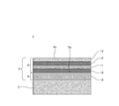
- 1 includes an optical substrate 2 and an antireflection film 3 provided on the optical substrate 2.
- the optical substrate 2 may be, for example, an optical element such as a lens or a film, and the form is not particularly limited.
- the lens include an in-vehicle lens, a monitoring camera lens, an interchangeable lens, and a television lens.
- the optical member 1 is used by being attached to the surface of an optical element such as a lens.
- Glass or resin is used for the material of the optical base material 2, and examples of the resin include polycarbonate, cycloolefin, polyimide, etc., but the glass transition temperature is 300 ° C. or higher in relation to the method for producing an antireflection film described later.
- the antireflection film 3 includes a reflectance adjusting film 4 and a photocatalytic film 5 provided between the reflectance adjusting film 4 and the optical substrate 2.
- the photocatalyst film 5 generates oxygen radicals when irradiated with light, and the oxygen radicals generated in the photocatalyst film 5 decompose the dirt attached to the surface 4a of the reflectivity adjusting film 4 in contact with the outside air.
- the surface 4a is prevented from being water repellent by the self-cleaning action caused by the oxygen radicals.
- the surface 4a is formed of a hydrophilic material.
- the surface 4a being “hydrophilic” means that the contact angle with water is 10 ° or less, and the contact angle is measured by the sessile drop method defined in JIS R 3257.
- the hydrophilic material forming the surface 4a include SiO 2 (silicon dioxide).
- the reflectance adjustment film 4 includes a first layer 10, a second layer 11 that is disposed on the surface 4 a side of the first layer 10 and has a higher refractive index than the first layer 10, and a second layer. 11 and the third layer 12 disposed on the surface 4a side and having a lower refractive index than the second layer 11.
- materials for forming the first layer 10 and the third layer 12 include SiO 2 , MgF 2 (magnesium fluoride), Si 3 N 4 (silicon nitride), and Al 2 O 3 (aluminum oxide).
- a low refractive index material having a refractive index of 1.6 or less can be exemplified.
- TiO 2 titanium dioxide
- ITO tin-doped indium oxide
- ZnO zinc oxide
- SnO 2 tin dioxide
- In 2 O 3 indium oxide
- Nb 2 O 5 niobium pentoxide
- Ta 2 O 5 tantalum pentoxide
- TiN titanium nitride
- ZrO zirconium oxide
- the surface 4a can be formed of the third layer 12 as shown in FIG.
- the hydrophilic surface layer 13 is formed on the surface 4a side of the third layer 12 as shown in FIG.
- the surface 4 a may be formed by the surface layer 13.
- the third layer 12 or the surface layer 13 forming the surface 4a may be formed in a porous shape having fine irregularities from the viewpoint of making the surface 4a hydrophilic. To form a solid.
- An intermediate layer may be provided between the first layer 10 and the second layer 11.
- Examples of the intermediate layer include those having an intermediate refractive index between the refractive index of the first layer 10 and the refractive index of the second layer 11.
- an intermediate layer may be provided between the second layer 11 and the third layer 12.
- the thicknesses of the first layer 10, the second layer 11, and the third layer 12 are appropriately set according to the refractive index of each layer, the wavelength range for suppressing reflection, and the like.
- the first layer 10 and the third layer 12 are made of SiO 2 and the second layer 11 is made of TiO 2 and the average reflectance is less than 1% in the wavelength range of 400 nm to 700 nm
- the thickness of the first layer 10 is preferably 15 to 40 nm
- the thickness of the second layer 11 is preferably 10 to 25 nm
- the thickness of the third layer 12 is preferably 20 to 100 nm.
- the entire thickness of the reflectance adjustment film 4 is 20 nm or more and less than 150 nm.
- the total thickness of the reflectance adjusting film 4 is less than 20 nm, there is a possibility that reflectance characteristics having an average reflectance of 1% or less cannot be obtained in the wavelength range of 400 nm to 700 nm. Moreover, when the thickness of the whole reflectance adjustment film
- the photocatalytic film 5 includes a photocatalytic active layer 14 containing TiO 2 (titanium dioxide).
- the photocatalytic active layer 14 may be a single layer as shown in FIG. 1 or a plurality of layers as shown in FIG.
- the material of the intermediate layer 15 interposed between two adjacent photocatalytic active layers 14 may be the low refractive index material (SiO 2 , MgF 2 , Si 3 N 4 etc.) and the high refractive index materials (ITO, ZnO, SnO 2 , In 2 O 3 , Nb 2 O 5 , Ta 2 O 5 , TiN, ZrO, etc.) excluding TiO 2 can be exemplified.
- the total thickness of the photocatalytic active layer 14 is 350 nm to 1000 nm, preferably 350 nm to 500 nm.
- membrane 5 is arrange
- each layer forming the reflectance adjustment film 4 and each layer forming the photocatalyst film 5 is a value measured by an optical film thickness meter (built in a film forming machine described later).
- the film thickness of the sample was measured by cross-sectional TEM (Transmission-Electron-Microscope) observation, and it was confirmed that the measured value of the optical film thickness meter and the measured value of TEM observation coincided between -3 nm and +3 nm.
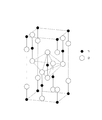
- the crystal structure of TiO 2 contained in the photocatalytically active layer 14 is an anatase structure.
- TiO 2 of anatase structure is excellent in photocatalytic activity as compared with TiO 2 of the rutile structure.
- the crystal structure of the anatase structure is tetragonal and has a structure in which Ti is surrounded by six O atoms.
- TiO 2 contained in the photocatalytic active layer 14 is doped with at least one element selected from the group consisting of N (nitrogen), S (sulfur), Cr (chromium), Sb (antimony), and Ce (cerium). May be. By doping these elements, the photocatalytic activity of the photocatalytic active layer 14 can be further increased.
- the doping amount is preferably 0.01 mol% or more and 0.05 mol% or less in the molar ratio between Ti and the doping element.
- a part of Ti ions on the surface of the TiO 2 film is replaced with cations (Cr 3+ , Sb 3+ , Ce 3+ ), or a part of oxygen ions on the surface of the TiO 2 film is anions (N, S (the valence is various Therefore, the photocatalytic activity can be improved by substituting with (not shown))).
- the doping element amount is less than 0.01 mol%, the improvement of the photocatalytic activity of the TiO 2 film by substitution of the above ions cannot be expected, and when the doping element amount exceeds 0.05 mol%, the doping element becomes a TiO 2 film. There is a risk of aggregation on the surface and reducing the photocatalytic activity of the TiO 2 film.
- the antireflection film 3 described above is manufactured by forming the photocatalyst film 5 and the reflectance adjustment film 4 on the optical base material 2 in this order, and vapor deposition can be used for film formation.
- a reflectance adjusting film including a first layer 10 having a low refractive index such as SiO 2, a second layer 11 having a high refractive index such as TiO 2 , and a third layer 12 having a low refractive index such as SiO 2.
- the film formation by the vapor deposition method 4 is known, and the film formation of the photocatalyst film 5 will be described below.
- Ti 3 O 5 titanium pentoxide
- Ti 3 O 5 titanium pentoxide
- the temperature of the optical substrate 2 is set to 300 ° C. or higher and 350 ° C. or lower. This makes it possible to promote the formation of TiO 2 in the anatase structure.
- the temperature of the optical substrate 2 is excessively low (for example, 200 ° C. or less), generation of amorphous TiO 2 that does not exhibit photocatalytic activity is promoted, and the temperature of the optical substrate 2 is excessively high (for example, 400 ° C. or more). This facilitates the generation of rutile TiO 2 .
- the photocatalytic active layer 14 is formed in an atmosphere into which oxygen is introduced, and the flow rate of oxygen is 100 ⁇ 1.69 ⁇ 10 ⁇ 3 Pa ⁇ m 3 / sec or more 120 ⁇ 1 in terms of 0 ° C. .69 ⁇ 10 ⁇ 3 Pa ⁇ m 3 / sec or less.
- the crystallinity of TiO 2 having an anatase structure can be increased, and the photocatalytic activity of the photocatalytic active layer 14 can be further increased.
- the photocatalytic film 5 formed on the optical substrate 2 is annealed, the temperature of the annealing atmosphere (hereinafter referred to as annealing temperature) is 350 ° C. or more and 400 ° C. or less, and the annealing time is 2 hours or more and 6 hours or less. And thereby, the sustainability of the photocatalytic activity of the photocatalytic active layer 14 can be enhanced.
- annealing temperature the temperature of the annealing atmosphere
- the annealing time is 2 hours or more and 6 hours or less.
- Duration of the photocatalytic activity by annealing the photocatalyst film 5 is estimated to be related to the decrease in the impurity level is included in the TiO 2, the impurity level contained in the TiO 2 is, like the oxygen deficiency level, TiO It is considered that the electron transition occurring in 2 becomes a trap level and the photocatalytic activity of the photocatalytic active layer 14 is lowered.
- ESR electron spin resonance
- the effect of sustaining the photocatalytic activity of the photocatalytic active layer 14 by annealing is also affected by the annealing atmosphere, and by annealing the photocatalytic film 5 in the air compared to the case where the photocatalytic film 5 is annealed in oxygen, the photocatalytic activity is increased.
- the sustaining effect can be enhanced.
- the dope is applied to the sample on which the TiO 2 film is formed.
- an ion implantation apparatus can be used, and as a doping method, for example, a method described in JP-A-9-262482 can be used. Then, after doping with a different element, the reflectance adjustment film 4 is formed.
- X-ray diffraction (XRD) measurement was performed on the obtained photocatalyst film, and the crystal structure of TiO 2 contained in the photocatalyst film was determined. analyzed.
- the measurement apparatus and measurement conditions used for the XRD measurement are as follows.
- ⁇ Device RINT-2500 (Rigaku) -Radiation source: Cu k ⁇ 55 kV, 280 mA ⁇
- FIG. 6 shows the XRD measurement results when the temperature of the optical substrate is 300 ° C. and the amount of oxygen introduced is 100 ⁇ 1.69 ⁇ 10 ⁇ 3 Pa ⁇ m 3 / sec.
- any XRD measurement result of FIG. 5 and FIG. 6 the XRD peak position coincides with the peak position (document value) of anatase type TiO 2 , but the XRD measurement result shown in FIG. 6 is shown in FIG.
- the baseline on the low angle side (2 ⁇ ⁇ 40 °) is lowered, and the intensity of each peak is high. This indicates that the crystallinity of TiO 2 is relatively high when the amount of oxygen introduced is 100 ⁇ 1.69 ⁇ 10 ⁇ 3 Pa ⁇ m 3 / sec.
- the temperature of the optical substrate when forming the SiO 2 film was the same as that when forming the photocatalytic film, and the amount of oxygen introduced was zero.
- the contact angle of the SiO 2 film on the sample surface with water was measured by the following procedure, and the photocatalyst film was measured based on the contact angle.
- the film thickness dependence of photocatalytic activity was evaluated.
- an automotive wax (trade name “New Willson” Willson) is rubbed against the sample surface using a cotton swab, and after 24 hours or more has passed since the wax application, the wax applied to the sample surface is removed. The sample was removed with a neutral detergent and water, and the contact angle ⁇ 1 with water on the sample surface from which the wax was removed was measured.
- the sample surface was irradiated with ultraviolet light, and after the irradiation, the contact angle ⁇ 2 of the sample surface with water was measured again.
- a UV-B ultraviolet lamp 20WGL20SE made by Sankyo Electric was used as the ultraviolet light source, and the irradiation conditions were UV illuminance of 3 mw / cm 2 and irradiation time of 40 minutes (corresponding to 7.2 J / cm 2 ).
- DM300 manufactured by Kyowa Interface Science was used as the contact angle measuring device. The above contact angle measurement procedure will be referred to as a WAX test below.
- Table 2 shows the measurement results of the contact angle ⁇ 2.
- the value of the contact angle ⁇ 2 in Table 2 is an average value of measured values obtained by measuring the contact angle three times for each sample.
- the contact angle ⁇ 1 was 50 ° or more in any of the evaluation samples.
- the contact angle ⁇ 2 after ultraviolet irradiation of a sample having a photocatalytic film thickness of 350 nm or more is 5 ° or less, which is so-called super hydrophilicity. From this measurement result, it is understood that the thickness of the photocatalyst film (total thickness of the photocatalytic active layer) is 350 nm or more in order to develop the self-cleaning action of TiO 2 contained in the photocatalyst film.
- annealing was performed in air by changing the annealing temperature and annealing time for the evaluation sample with a photocatalyst film thickness of 350 nm and the evaluation sample with a photocatalyst film thickness of 500 nm. Then, the WAX test is repeated on the annealed sample, and the sustainability of the photocatalytic activity of the photocatalytic film is evaluated based on the number of tests in which the contact angle with water on the sample surface after ultraviolet light irradiation is 5 ° or less. did.
- the sustainability evaluation results are shown in Table 3.
- the number of tests in Table 3 is the number of times when the annealing time is 4 hours.
- the durability of the photocatalytic activity of the photocatalytic film can be enhanced by annealing in air at an annealing temperature of 350 ° C. to 400 ° C.
- an appropriate annealing temperature depends on the thickness of the photocatalyst film, and the annealing temperature is preferably 350 ° C. when the thickness of the photocatalytic film is 350 nm, and 400 ° C. is preferable when the thickness of the photocatalyst film is 500 nm.
- the number of tests in Table 3 is the number of times when the annealing time is 4 hours, but the same results as in Table 3 were obtained when the annealing time ranged from 2 to 6 hours.
- the optical members of Experimental Example 1, Experimental Example 2, and Experimental Example 4 to Experimental Example 7 have the configuration shown in FIG. 1, and a single-layer photocatalytic film 5 made of TiO 2 and a reflectance adjusting film 4 are provided. sequentially deposited on the optical substrate 2, the reflectivity adjustment layer 4, in order from the optical substrate 2 side, a first layer 10 made of SiO 2, and a second layer 11 consisting of TiO 2, SiO 2 And a third layer 12 made of
- the optical member of Experimental Example 3 has the configuration shown in FIG.
- the optical member of Experimental Example 8 includes, on the optical base 2 , a single-layer photocatalytic film 5 made of TiO 2 and a single-layer reflectance adjustment film 4 made of SiO 2 in this order. The film was formed on top.
- white plate glass manufactured by FD110 HOYA was used as the optical substrate 2.
- the single-layer photocatalytic film 5 made of TiO 2 uses Ti 3 O 5 as an evaporation material, the temperature of the optical substrate 2 is 350 ° C., and the amount of oxygen introduced is 100 ⁇ 1.69 ⁇ 10 ⁇ 3.
- the film was formed by electron beam evaporation at Pa ⁇ m 3 / sec. Then, the photocatalyst film 5 formed on the optical substrate 2 was annealed in air under the conditions of an annealing temperature of 350 ° C. and an annealing time of 4 hours.
- the second layer 11 made of TiO 2 of the reflectivity adjusting film 4 uses Ti 3 O 5 as a deposition material, the temperature of the optical substrate 2 is 350 ° C., and the amount of oxygen introduced is 100 ⁇ 1.
- the film was formed by electron beam evaporation at 69 ⁇ 10 ⁇ 3 Pa ⁇ m 3 / sec.
- the first layer 10, the third layer 12, and the surface layer 13 made of SiO 2 of the reflectance adjustment film 4 use SiO 2 as a vapor deposition material, set the temperature of the optical substrate 2 to 350 ° C., and A film was formed by electron beam evaporation with the amount of oxygen introduced being zero.
- the first layer 10 and the third layer 12 made of MgF 2 of the reflectance adjustment film 4 use MgF 2 as a vapor deposition material, the temperature of the optical substrate 2 is set to 350 ° C., and the amount of oxygen introduced.
- the film was formed by electron beam evaporation, with 0 being zero.
- the reflectance characteristics were evaluated based on the average reflectance in the wavelength range of 400 nm to 700 nm, the presence or absence of ripple (variation) in the reflectance characteristic curve in the wavelength range of 400 nm to 700 nm, and the degree of ripple.
- the average reflectance is a value obtained by measuring the reflectance of each wavelength at a wavelength of 1 nm and dividing the total reflectance by the number of measurements. When the average reflectance is 0.5% or less and there is no ripple, the evaluation is A. When the average reflectance is 1.0% or less and there is a relatively weak ripple, the evaluation is B.
- the average reflectance is 1 A C evaluation was given when the ratio was 0.0% or less and there was a relatively strong ripple, and a D evaluation was given when the average reflectance was greater than 1.0%. Further, the self-cleaning action was evaluated based on the contact angle of the surface 4a of the reflectance adjusting film 4 after irradiation with ultraviolet light with water 10 times after performing the WAX test 10 times.
- Table 4 shows the evaluation results of the reflectance characteristics and the self-cleaning action.
- the interface 5a on the reflectance adjustment film 4 side of the photocatalyst film 5 extends from the surface 4a of the reflectance adjustment film 4. It is arranged at a position of 315 nm deeper than 150 nm. In this case, the transport of oxygen radicals generated in the photocatalyst film 5 to the surface 4a is hindered, and the self-cleaning action is reduced. As a result, the contact angle of the surface 4a is 22.4 °.
- the contact angle of the surface 4a is 15.2 °.
- the average reflectance in the wavelength range of 400 to 700 nm is 1.3%. It lacks practicality as an antireflection film.
- the total thickness of the reflectance adjustment film 4 is 20 nm or more and less than 150 nm
- the interface 5a of the photocatalyst film 5 is disposed at a position 150 nm or less from the surface 4a
- the thickness of the photocatalyst film 5 is 350 nm or more and 1000 nm or less.
- the average reflectance in the wavelength range of 400 to 700 nm is 1.0% or less, which is practical as an antireflection film. Is provided.
- the contact angle of the surface 4a is 5 ° or less, and the hydrophilicity of the surface 4a is maintained by the self-cleaning action.
- the thickness of the photocatalytic film 5 is 350 nm or more and 500 nm or less
- the average reflectance in the wavelength range of 400 to 700 nm is 0.5% or less and the wavelength is 400 nm.
- the reflectance characteristic curve in the range of ⁇ 700 nm is flat without ripples. From the above results, the thickness of the photocatalyst film 5 is preferably 350 nm or more and 500 nm or less, whereby the reflectance characteristics of the antireflection film 3 can be improved.
- the optical members of Experimental Examples 9 to 11 have the same configuration as the optical member of Experimental Example 2 described above. However, the film formation conditions of the single-layer photocatalyst film 5 made of TiO 2 are different for each experimental example.
- the temperature of the optical substrate 2 is 350 ° C.
- the amount of oxygen introduced is 100 ⁇ .
- the film was formed by electron beam evaporation at 1.69 ⁇ 10 ⁇ 3 Pa ⁇ m 3 / sec.
- the temperature of the optical substrate 2 is set to 400 ° C., and the amount of oxygen introduced is set to 100 ⁇ 1.69 ⁇ 10 ⁇ 3 Pa ⁇ m 3 / sec. did.
- the temperature of the optical substrate 2 is set to 200 ° C., and the amount of oxygen introduced is set to 100 ⁇ 1.69 ⁇ 10 ⁇ 3 Pa ⁇ m 3 / sec. did.
- the crystal structure of TiO 2 contained in the photocatalyst film 5 thus formed was analyzed by XRD measurement
- the optical member of Experimental Example 9 has an anatase structure
- the optical member of Experimental Example 10 has a rutile structure.
- the optical member of Example 11 had an amorphous structure.
- Table 5 shows the evaluation results of the relationship between the TiO 2 crystal structure and the self-cleaning action.
- the contact angle of the surface 4a of the reflectance adjusting film 4 is 30 °, and the photocatalytic film 5 has an amorphous structure.
- the contact angle of the surface 4a of the reflectance adjusting film 4 is 50 °
- the photocatalytic film 5 of Experimental Example 9 made of TiO 2 having an anatase structure is used.
- the contact angle of the surface 4a of the reflectance adjusting film 4 is 4.8 °, and the hydrophilicity of the surface 4a is maintained by the self-cleaning action.
- the crystal structure of TiO 2 contained in the photocatalyst film 5 is an anatase structure, whereby the photocatalytic activity of the photocatalyst film 5 can be enhanced and the self-cleaning action can be enhanced.
- the optical members of Experimental Examples 12 to 14 have the same configuration as the optical member of Experimental Example 2 described above. However, the single-layer photocatalytic film 5 containing TiO 2 is doped with a different element for each experimental example.
- the optical member of Experimental example 12 is doped with N (nitrogen), and the optical member of Experimental example 13 Cr (chromium) was doped, and the optical member of Experimental Example 14 was doped with Ce (cerium).
- Table 6 shows the evaluation results of the relationship between the doping element and the self-cleaning action.
- any one of the optical member of Experimental Example 12 doped with N, the optical member of Experimental Example 13 doped with Cr, and the optical member of Experimental Example 14 doped with Ce was the above experimental example.
- the average reflectance in the wavelength range of 400 to 700 nm is small, and the contact angle of the surface 4 a of the reflectance adjustment film 4 is also small.
- TiO 2 contained in the photocatalyst film 5 may be doped with N, Cr, and Ce, and by doping these elements, the photocatalytic activity of the photocatalyst film 5 is enhanced and the self-cleaning action is achieved. Can be enhanced.
- the film thickness of the intermediate layer 15 made of SiO 2 of the photocatalytic film 5 is different for each experimental example.
- the optical member of Experimental Example 15 is 1 nm
- the optical member of Experimental Example 16 is 2 nm
- the optical member of Experimental Example 17 is The thickness was 3 nm.
- white plate glass manufactured by FD110 HOYA was used as the optical substrate 2.
- the first photocatalytic active layer 14 and the second photocatalytic active layer 14 made of TiO 2 use Ti 3 O 5 as a deposition material, the temperature of the optical substrate 2 is set to 350 ° C., and the amount of oxygen introduced is set.
- the film was formed by electron beam evaporation at 100 ⁇ 1.69 ⁇ 10 ⁇ 3 Pa ⁇ m 3 / sec.
- the intermediate layer 15 made of SiO 2 is a SiO 2 used as the evaporation material, the temperature of the optical substrate 2 and 350 ° C., and the amount of introduced oxygen as 0, was deposited by electron beam evaporation.
- the photocatalyst film 5 formed on the optical substrate 2 was annealed in air under the conditions of an annealing temperature of 350 ° C. and an annealing time of 4 hours.
- the second layer 11 made of TiO 2 of the reflectivity adjusting film 4 uses Ti 3 O 5 as a deposition material, the temperature of the optical substrate 2 is 350 ° C., and the amount of oxygen introduced is 100 ⁇ 1.
- the film was formed by electron beam evaporation at 69 ⁇ 10 ⁇ 3 Pa ⁇ m 3 / sec.
- the first layer 10, the third layer 12, and the surface layer 13 made of SiO 2 of the reflectance adjustment film 4 use SiO 2 as a vapor deposition material, set the temperature of the optical substrate 2 to 350 ° C., and A film was formed by electron beam evaporation with the amount of oxygen introduced being zero.
- the above-described WAX test was performed 10 times on the optical members of Experimental Examples 15 to 17, and the intermediate layer of the photocatalytic film 5 was determined based on the contact angle of the surface 4a of the reflectance adjustment film 4 after ultraviolet light irradiation with water. The relationship between the thickness of 15 and the self-cleaning action was evaluated.
- Table 7 shows the evaluation results of the relationship between the thickness of the intermediate layer 15 and the self-cleaning action.
- the photocatalytic film 5 is a two-layer photocatalytic active layer 14 via the intermediate layer 15. It is substantially the same except whether or not it is divided.
- the average reflectance in the wavelength range of 400 to 700 nm of each optical member of Experimental Example 15 to Experimental Example 17 is 0.5% or less, similar to that of the optical member of Experimental Example 2, and Experimental Examples 15 to The contact angle of the surface 4a of the reflectivity adjusting film 4 of each optical member in Experimental Example 17 is 4.8 ° as in the optical member in Experimental Example 2. From the above results, it can be seen that the photocatalytic film 5 may include two layers of the photocatalytic active layer 14 via the intermediate layer 15.
- the antireflection film disclosed in this specification is an antireflection film provided on an optical substrate, and the antireflection film is provided on the first layer and the first layer.
- a second layer having a higher refractive index than that of the first layer and a third layer having a lower refractive index than the second layer and disposed on the surface side of the second layer.
- a reflectance adjustment film having a thickness from the surface of 20 nm or more and less than 150 nm, and one or more photocatalytic active layers containing titanium dioxide, and the reflectance adjustment film and the optical substrate.
- a photocatalyst film having a total thickness of 350 nm to 1000 nm of the photocatalytic active layer, the interface on the reflectance adjusting film side being disposed at a position of 150 nm or less from the surface.
- the total thickness of the photocatalytic active layer is 350 nm or more and 500 nm or less.
- the antireflection film disclosed in the present specification is a single layer of the photocatalytic active layer included in the photocatalytic film.
- the crystal structure of titanium dioxide contained in the photocatalytic active layer is an anatase structure.
- the antireflection film disclosed in the present specification is an antireflection film in which the photocatalytic active layer further contains one or more elements selected from the group consisting of nitrogen, sulfur, chromium, antimony, and cerium.
- the third layer is made of silicon dioxide and forms the surface.
- the optical member disclosed in the present specification has the antireflection film provided on an optical substrate.
- the optical substrate is a lens
- the present invention can be used for optical members such as a lens and a cover of a camera installed outdoors such as a surveillance camera and an in-vehicle camera.
Landscapes
- Chemical & Material Sciences (AREA)
- Physics & Mathematics (AREA)
- Chemical Kinetics & Catalysis (AREA)
- Engineering & Computer Science (AREA)
- Materials Engineering (AREA)
- Organic Chemistry (AREA)
- General Physics & Mathematics (AREA)
- Optics & Photonics (AREA)
- Inorganic Chemistry (AREA)
- Health & Medical Sciences (AREA)
- Ophthalmology & Optometry (AREA)
- General Health & Medical Sciences (AREA)
- Catalysts (AREA)
- Surface Treatment Of Optical Elements (AREA)
- Laminated Bodies (AREA)
- Surface Treatment Of Glass (AREA)
- Physical Vapour Deposition (AREA)
Abstract
Ce film antireflet, qui est disposé sur un substrat optique d'un élément optique, comprend : un film de modulation d'indice de réfraction qui comprend une première couche, une deuxième couche 11 qui a un indice de réfraction plus élevé que la première couche 10, et une troisième couche 12 qui a un indice de réfraction inférieur à celui de la deuxième couche 11, et qui a une épaisseur à partir d'une surface de 20 nm ou plus mais inférieure à 150 nm; et un film de photocatalyseur qui comprend une ou plusieurs couches actives de photocatalyseur qui contiennent du dioxyde de titane, et qui est disposée entre le film de modulation d'indice de réfraction et le substrat optique, de telle sorte qu'une interface côté film de modulation d'indice de réfraction 5a est agencée à une position à l'intérieur de 150 nm à partir de la surface 4a et que l'épaisseur totale des couches actives de photocatalyseur 14 est de 350 nm à 1 000 nm (inclus).
Priority Applications (6)
| Application Number | Priority Date | Filing Date | Title |
|---|---|---|---|
| CN202511044355.5A CN120630359A (zh) | 2017-04-12 | 2018-03-23 | 防反射膜及光学部件 |
| JP2019512408A JP6728484B2 (ja) | 2017-04-12 | 2018-03-23 | 反射防止膜及び光学部材 |
| CN201880024723.1A CN110520764A (zh) | 2017-04-12 | 2018-03-23 | 防反射膜及光学部件 |
| CN202511044354.0A CN120630358A (zh) | 2017-04-12 | 2018-03-23 | 防反射膜及光学部件 |
| CN202511044356.XA CN120630360A (zh) | 2017-04-12 | 2018-03-23 | 防反射膜及光学部件 |
| US16/591,447 US11703614B2 (en) | 2017-04-12 | 2019-10-02 | Antireflection film and optical member |
Applications Claiming Priority (2)
| Application Number | Priority Date | Filing Date | Title |
|---|---|---|---|
| JP2017-079008 | 2017-04-12 | ||
| JP2017079008 | 2017-04-12 |
Related Child Applications (1)
| Application Number | Title | Priority Date | Filing Date |
|---|---|---|---|
| US16/591,447 Continuation US11703614B2 (en) | 2017-04-12 | 2019-10-02 | Antireflection film and optical member |
Publications (1)
| Publication Number | Publication Date |
|---|---|
| WO2018190105A1 true WO2018190105A1 (fr) | 2018-10-18 |
Family
ID=63793439
Family Applications (1)
| Application Number | Title | Priority Date | Filing Date |
|---|---|---|---|
| PCT/JP2018/011924 Ceased WO2018190105A1 (fr) | 2017-04-12 | 2018-03-23 | Film antireflet et élément optique |
Country Status (4)
| Country | Link |
|---|---|
| US (1) | US11703614B2 (fr) |
| JP (1) | JP6728484B2 (fr) |
| CN (5) | CN120630360A (fr) |
| WO (1) | WO2018190105A1 (fr) |
Cited By (1)
| Publication number | Priority date | Publication date | Assignee | Title |
|---|---|---|---|---|
| WO2020110523A1 (fr) * | 2018-11-28 | 2020-06-04 | 富士フイルム株式会社 | Matériau composite photocatalytique, élément de protection pour capteurs, élément de protection pour matériaux de construction, élément de protection pour véhicules, élément de protection pour récipients de refroidissement, élément de protection pour caméras de sécurité, capteur, matériaux de construction, véhicule, récipient de refroidissement et caméra de sécurité |
Families Citing this family (2)
| Publication number | Priority date | Publication date | Assignee | Title |
|---|---|---|---|---|
| JPWO2021261225A1 (fr) * | 2020-06-23 | 2021-12-30 | ||
| CN116694217B (zh) * | 2023-07-03 | 2024-07-23 | 天津市职业大学 | 一种太阳光催化自清洁涂料及其制备和应用方法 |
Citations (5)
| Publication number | Priority date | Publication date | Assignee | Title |
|---|---|---|---|---|
| JP2002028495A (ja) * | 2000-05-11 | 2002-01-29 | Ichikoh Ind Ltd | 可視光線応答型光触媒 |
| JP2003287601A (ja) * | 2002-03-27 | 2003-10-10 | Murakami Corp | 複合材 |
| JP2004294521A (ja) * | 2003-03-25 | 2004-10-21 | Sanyo Electric Co Ltd | ピックアップ用対物レンズ |
| WO2008123553A1 (fr) * | 2007-04-04 | 2008-10-16 | Asahi Glass Company, Limited | Elément antisalissure et verre feuilleté utilisant ledit élément |
| WO2017056598A1 (fr) * | 2015-09-29 | 2017-04-06 | 富士フイルム株式会社 | Film multicouche hydrophile et son procédé de fabrication, et système d'imagerie |
Family Cites Families (17)
| Publication number | Priority date | Publication date | Assignee | Title |
|---|---|---|---|---|
| JP3844823B2 (ja) | 1996-01-22 | 2006-11-15 | 財団法人石油産業活性化センター | 光触媒、光触媒の製造方法および光触媒反応方法 |
| JP2004318054A (ja) | 2003-03-28 | 2004-11-11 | Fuji Photo Film Co Ltd | 偏光板及びその製造方法、並びに画像表示装置 |
| CN1768280A (zh) * | 2003-03-28 | 2006-05-03 | 富士胶片株式会社 | 偏振片及其制备方法,和图象显示装置 |
| JPWO2004100731A1 (ja) * | 2003-05-14 | 2006-07-13 | 株式会社村上開明堂 | 防曇鏡 |
| JP4655581B2 (ja) * | 2003-11-10 | 2011-03-23 | 三菱マテリアル株式会社 | オーバーコート塗料及び該塗料を用いて形成した多層光触媒塗膜 |
| FR2869897B1 (fr) * | 2004-05-10 | 2006-10-27 | Saint Gobain | Substrat a revetement photocatalytique |
| US20090267270A1 (en) * | 2005-09-20 | 2009-10-29 | Konica Minolta Opto, Inc. | Process for producing film with concavo-convex pattern |
| JP2008003390A (ja) | 2006-06-23 | 2008-01-10 | Bridgestone Corp | 反射防止膜及び光学フィルター |
| JP5271575B2 (ja) * | 2007-03-20 | 2013-08-21 | 富士フイルム株式会社 | 反射防止フィルム、偏光板、および画像表示装置 |
| CN201327536Y (zh) * | 2008-12-09 | 2009-10-14 | 温州医学院眼视光研究院 | 光诱导防污防雾自清洁的树脂镜片 |
| CA2765177A1 (fr) * | 2009-06-11 | 2010-12-16 | Essilor International(Compagnie Generale D'optique) | Composition de revetement durcissable modifiee avec un agent tensioactif pouvant etre divise afin d'ameliorer l'adherence dans des piles de revetement multicouche |
| TWI436096B (zh) * | 2010-12-22 | 2014-05-01 | Extend Optronics Corp | 均光抗眩結構及發光裝置 |
| EP2808710A4 (fr) * | 2012-01-25 | 2016-04-06 | Konica Minolta Advanced Layers | Film optique |
| US20140248507A1 (en) * | 2013-03-01 | 2014-09-04 | Vladimir Kleptsyn | Anti-reflective coating |
| WO2014199990A1 (fr) * | 2013-06-14 | 2014-12-18 | コニカミノルタ株式会社 | Film multicouche dérivatif |
| JP6513486B2 (ja) | 2015-05-27 | 2019-05-15 | ジオマテック株式会社 | 防曇性反射防止膜、防曇性反射防止膜付きカバー基体及び防曇性反射防止膜の製造方法 |
| CN106977113A (zh) * | 2016-01-19 | 2017-07-25 | 精工爱普生株式会社 | 透光性部件、钟表及透光性部件的制造方法 |
-
2018
- 2018-03-23 CN CN202511044356.XA patent/CN120630360A/zh active Pending
- 2018-03-23 CN CN201880024723.1A patent/CN110520764A/zh active Pending
- 2018-03-23 CN CN202110985368.8A patent/CN113703077A/zh active Pending
- 2018-03-23 CN CN202511044354.0A patent/CN120630358A/zh active Pending
- 2018-03-23 WO PCT/JP2018/011924 patent/WO2018190105A1/fr not_active Ceased
- 2018-03-23 CN CN202511044355.5A patent/CN120630359A/zh active Pending
- 2018-03-23 JP JP2019512408A patent/JP6728484B2/ja active Active
-
2019
- 2019-10-02 US US16/591,447 patent/US11703614B2/en active Active
Patent Citations (5)
| Publication number | Priority date | Publication date | Assignee | Title |
|---|---|---|---|---|
| JP2002028495A (ja) * | 2000-05-11 | 2002-01-29 | Ichikoh Ind Ltd | 可視光線応答型光触媒 |
| JP2003287601A (ja) * | 2002-03-27 | 2003-10-10 | Murakami Corp | 複合材 |
| JP2004294521A (ja) * | 2003-03-25 | 2004-10-21 | Sanyo Electric Co Ltd | ピックアップ用対物レンズ |
| WO2008123553A1 (fr) * | 2007-04-04 | 2008-10-16 | Asahi Glass Company, Limited | Elément antisalissure et verre feuilleté utilisant ledit élément |
| WO2017056598A1 (fr) * | 2015-09-29 | 2017-04-06 | 富士フイルム株式会社 | Film multicouche hydrophile et son procédé de fabrication, et système d'imagerie |
Cited By (1)
| Publication number | Priority date | Publication date | Assignee | Title |
|---|---|---|---|---|
| WO2020110523A1 (fr) * | 2018-11-28 | 2020-06-04 | 富士フイルム株式会社 | Matériau composite photocatalytique, élément de protection pour capteurs, élément de protection pour matériaux de construction, élément de protection pour véhicules, élément de protection pour récipients de refroidissement, élément de protection pour caméras de sécurité, capteur, matériaux de construction, véhicule, récipient de refroidissement et caméra de sécurité |
Also Published As
| Publication number | Publication date |
|---|---|
| CN120630360A (zh) | 2025-09-12 |
| CN110520764A (zh) | 2019-11-29 |
| CN113703077A (zh) | 2021-11-26 |
| JP6728484B2 (ja) | 2020-07-22 |
| US20200033507A1 (en) | 2020-01-30 |
| US11703614B2 (en) | 2023-07-18 |
| JPWO2018190105A1 (ja) | 2020-02-06 |
| CN120630358A (zh) | 2025-09-12 |
| CN120630359A (zh) | 2025-09-12 |
Similar Documents
| Publication | Publication Date | Title |
|---|---|---|
| CN108463745B (zh) | 亲水性多层膜及其制造方法和摄像系统 | |
| US8614848B2 (en) | Electrochromic element and method of forming same | |
| EP2804026B1 (fr) | Produit optique et son procédé de fabrication | |
| Moghal et al. | High-performance, single-layer antireflective optical coatings comprising mesoporous silica nanoparticles | |
| EP3081967A1 (fr) | Lentille ophtalmique comprenant une base de matériau polymère avec un revêtement à structure multicouche interférentielle antiréfléchissante, anti-iridescente et avec filtre ir | |
| JP6269665B2 (ja) | 光学フィルタ、光学フィルタの製造方法 | |
| Wang et al. | Design and sol–gel preparation of SiO2/TiO2 and SiO2/SnO2/SiO2–SnO2 multilayer antireflective coatings | |
| JP6728484B2 (ja) | 反射防止膜及び光学部材 | |
| US20130202866A1 (en) | Mechanically stable nanoparticle thin film coatings and methods of producing the same | |
| US20170151754A1 (en) | Optical member including antireflection film and method of manufacturing the same | |
| DE112010001362T5 (de) | Verfahren zur Erzeugung omnidirektionaler, mehrschichtigter photonischer Strukturen | |
| CN106574985A (zh) | 防反射膜及具备防反射膜的光学部件 | |
| TW201348758A (zh) | 紅外截止濾光片及鏡頭模組 | |
| JP2016224113A (ja) | 防曇性反射防止膜、防曇性反射防止膜付きカバー基体及び防曇性反射防止膜の製造方法 | |
| WO2016136261A1 (fr) | Film antireflet, et élément optique | |
| JP2020024237A (ja) | 光学製品 | |
| CN103454709A (zh) | 红外截止滤光片及镜头模组 | |
| JP6989289B2 (ja) | 親水性反射防止膜付きレンズ及びその製造方法 | |
| US12578519B2 (en) | Optical coating for organic surface treatments | |
| Vasiliu et al. | SiO x-P2O5 films—Promising components in photonic structure | |
| JP6338503B2 (ja) | 光学素子および光学素子の製造方法 | |
| JP7468624B2 (ja) | 光学部材 | |
| DE112022007775T5 (de) | Mehrschichtfilm, optisches element, das den mehrschichtfilm beinhaltet, und verfahren zum herstellen von mehrschichtfilm | |
| JP2024158884A (ja) | 反射調整膜、光学部材及びレンズユニット | |
| JP6153368B2 (ja) | 車両アウターミラー用有色防曇鏡 |
Legal Events
| Date | Code | Title | Description |
|---|---|---|---|
| 121 | Ep: the epo has been informed by wipo that ep was designated in this application |
Ref document number: 18783906 Country of ref document: EP Kind code of ref document: A1 |
|
| ENP | Entry into the national phase |
Ref document number: 2019512408 Country of ref document: JP Kind code of ref document: A |
|
| NENP | Non-entry into the national phase |
Ref country code: DE |
|
| 122 | Ep: pct application non-entry in european phase |
Ref document number: 18783906 Country of ref document: EP Kind code of ref document: A1 |