WO2018235590A1 - Procédé de production de cartes de circuit imprimé et encre conductrice - Google Patents
Procédé de production de cartes de circuit imprimé et encre conductrice Download PDFInfo
- Publication number
- WO2018235590A1 WO2018235590A1 PCT/JP2018/021514 JP2018021514W WO2018235590A1 WO 2018235590 A1 WO2018235590 A1 WO 2018235590A1 JP 2018021514 W JP2018021514 W JP 2018021514W WO 2018235590 A1 WO2018235590 A1 WO 2018235590A1
- Authority
- WO
- WIPO (PCT)
- Prior art keywords
- conductive ink
- transfer film
- substrate
- wiring
- layer
- Prior art date
- Legal status (The legal status is an assumption and is not a legal conclusion. Google has not performed a legal analysis and makes no representation as to the accuracy of the status listed.)
- Ceased
Links
Images



Classifications
-
- H—ELECTRICITY
- H05—ELECTRIC TECHNIQUES NOT OTHERWISE PROVIDED FOR
- H05K—PRINTED CIRCUITS; CASINGS OR CONSTRUCTIONAL DETAILS OF ELECTRIC APPARATUS; MANUFACTURE OF ASSEMBLAGES OF ELECTRICAL COMPONENTS
- H05K3/00—Apparatus or processes for manufacturing printed circuits
- H05K3/10—Apparatus or processes for manufacturing printed circuits in which conductive material is applied to the insulating support in such a manner as to form the desired conductive pattern
- H05K3/20—Apparatus or processes for manufacturing printed circuits in which conductive material is applied to the insulating support in such a manner as to form the desired conductive pattern by affixing prefabricated conductor pattern
- H05K3/207—Apparatus or processes for manufacturing printed circuits in which conductive material is applied to the insulating support in such a manner as to form the desired conductive pattern by affixing prefabricated conductor pattern using a prefabricated paste pattern, ink pattern or powder pattern
-
- C—CHEMISTRY; METALLURGY
- C09—DYES; PAINTS; POLISHES; NATURAL RESINS; ADHESIVES; COMPOSITIONS NOT OTHERWISE PROVIDED FOR; APPLICATIONS OF MATERIALS NOT OTHERWISE PROVIDED FOR
- C09D—COATING COMPOSITIONS, e.g. PAINTS, VARNISHES OR LACQUERS; FILLING PASTES; CHEMICAL PAINT OR INK REMOVERS; INKS; CORRECTING FLUIDS; WOODSTAINS; PASTES OR SOLIDS FOR COLOURING OR PRINTING; USE OF MATERIALS THEREFOR
- C09D11/00—Inks
- C09D11/30—Inkjet printing inks
- C09D11/38—Inkjet printing inks characterised by non-macromolecular additives other than solvents, pigments or dyes
-
- C—CHEMISTRY; METALLURGY
- C09—DYES; PAINTS; POLISHES; NATURAL RESINS; ADHESIVES; COMPOSITIONS NOT OTHERWISE PROVIDED FOR; APPLICATIONS OF MATERIALS NOT OTHERWISE PROVIDED FOR
- C09D—COATING COMPOSITIONS, e.g. PAINTS, VARNISHES OR LACQUERS; FILLING PASTES; CHEMICAL PAINT OR INK REMOVERS; INKS; CORRECTING FLUIDS; WOODSTAINS; PASTES OR SOLIDS FOR COLOURING OR PRINTING; USE OF MATERIALS THEREFOR
- C09D11/00—Inks
- C09D11/52—Electrically conductive inks
-
- H—ELECTRICITY
- H01—ELECTRIC ELEMENTS
- H01B—CABLES; CONDUCTORS; INSULATORS; SELECTION OF MATERIALS FOR THEIR CONDUCTIVE, INSULATING OR DIELECTRIC PROPERTIES
- H01B13/00—Apparatus or processes specially adapted for manufacturing conductors or cables
-
- H—ELECTRICITY
- H05—ELECTRIC TECHNIQUES NOT OTHERWISE PROVIDED FOR
- H05K—PRINTED CIRCUITS; CASINGS OR CONSTRUCTIONAL DETAILS OF ELECTRIC APPARATUS; MANUFACTURE OF ASSEMBLAGES OF ELECTRICAL COMPONENTS
- H05K1/00—Printed circuits
- H05K1/02—Details
- H05K1/09—Use of materials for the conductive, e.g. metallic pattern
- H05K1/092—Dispersed materials, e.g. conductive pastes or inks
- H05K1/097—Inks comprising nanoparticles and specially adapted for being sintered at low temperature
-
- H—ELECTRICITY
- H05—ELECTRIC TECHNIQUES NOT OTHERWISE PROVIDED FOR
- H05K—PRINTED CIRCUITS; CASINGS OR CONSTRUCTIONAL DETAILS OF ELECTRIC APPARATUS; MANUFACTURE OF ASSEMBLAGES OF ELECTRICAL COMPONENTS
- H05K3/00—Apparatus or processes for manufacturing printed circuits
- H05K3/10—Apparatus or processes for manufacturing printed circuits in which conductive material is applied to the insulating support in such a manner as to form the desired conductive pattern
- H05K3/12—Apparatus or processes for manufacturing printed circuits in which conductive material is applied to the insulating support in such a manner as to form the desired conductive pattern using thick film techniques, e.g. printing techniques to apply the conductive material or similar techniques for applying conductive paste or ink patterns
- H05K3/1241—Apparatus or processes for manufacturing printed circuits in which conductive material is applied to the insulating support in such a manner as to form the desired conductive pattern using thick film techniques, e.g. printing techniques to apply the conductive material or similar techniques for applying conductive paste or ink patterns by ink-jet printing or drawing by dispensing
- H05K3/125—Apparatus or processes for manufacturing printed circuits in which conductive material is applied to the insulating support in such a manner as to form the desired conductive pattern using thick film techniques, e.g. printing techniques to apply the conductive material or similar techniques for applying conductive paste or ink patterns by ink-jet printing or drawing by dispensing by ink-jet printing
-
- H—ELECTRICITY
- H05—ELECTRIC TECHNIQUES NOT OTHERWISE PROVIDED FOR
- H05K—PRINTED CIRCUITS; CASINGS OR CONSTRUCTIONAL DETAILS OF ELECTRIC APPARATUS; MANUFACTURE OF ASSEMBLAGES OF ELECTRICAL COMPONENTS
- H05K2201/00—Indexing scheme relating to printed circuits covered by H05K1/00
- H05K2201/01—Dielectrics
- H05K2201/0137—Materials
- H05K2201/0145—Polyester, e.g. polyethylene terephthalate [PET], polyethylene naphthalate [PEN]
-
- H—ELECTRICITY
- H05—ELECTRIC TECHNIQUES NOT OTHERWISE PROVIDED FOR
- H05K—PRINTED CIRCUITS; CASINGS OR CONSTRUCTIONAL DETAILS OF ELECTRIC APPARATUS; MANUFACTURE OF ASSEMBLAGES OF ELECTRICAL COMPONENTS
- H05K2201/00—Indexing scheme relating to printed circuits covered by H05K1/00
- H05K2201/02—Fillers; Particles; Fibers; Reinforcement materials
- H05K2201/0203—Fillers and particles
- H05K2201/0242—Shape of an individual particle
- H05K2201/026—Nanotubes or nanowires
-
- H—ELECTRICITY
- H05—ELECTRIC TECHNIQUES NOT OTHERWISE PROVIDED FOR
- H05K—PRINTED CIRCUITS; CASINGS OR CONSTRUCTIONAL DETAILS OF ELECTRIC APPARATUS; MANUFACTURE OF ASSEMBLAGES OF ELECTRICAL COMPONENTS
- H05K2203/00—Indexing scheme relating to apparatus or processes for manufacturing printed circuits covered by H05K3/00
- H05K2203/01—Tools for processing; Objects used during processing
- H05K2203/0147—Carriers and holders
- H05K2203/0156—Temporary polymeric carrier or foil, e.g. for processing or transferring
-
- H—ELECTRICITY
- H05—ELECTRIC TECHNIQUES NOT OTHERWISE PROVIDED FOR
- H05K—PRINTED CIRCUITS; CASINGS OR CONSTRUCTIONAL DETAILS OF ELECTRIC APPARATUS; MANUFACTURE OF ASSEMBLAGES OF ELECTRICAL COMPONENTS
- H05K2203/00—Indexing scheme relating to apparatus or processes for manufacturing printed circuits covered by H05K3/00
- H05K2203/11—Treatments characterised by their effect, e.g. heating, cooling, roughening
- H05K2203/1131—Sintering, i.e. fusing of metal particles to achieve or improve electrical conductivity
Definitions
- the present invention relates to a method of manufacturing a wiring substrate and a conductive ink.
- a wiring board in which a wiring pattern is formed on a substrate is known.
- a method of forming such a wiring pattern a method of forming a wiring pattern by etching a metal layer provided on a substrate, a method of forming a wiring pattern using a conductive paste or a conductive ink, and And a method of forming a wiring pattern by electroless plating.
- Patent Document 1 shows a method of manufacturing a wiring pattern using a conductive ink (a method of manufacturing a wiring substrate). Specifically, after peeling the support film from the transfer film on which the support film, the adhesive layer, the conductive layer (wiring pattern) obtained using the conductive ink, and the protective layer are laminated in this order, the adhesive layer is removed. A method of bonding the conductive layer on the substrate via the substrate is disclosed (claims 1, 4 and the like).
- the inventor used a conductive ink from the side opposite to the support for a specific transfer film in which the support, the protective layer, and the receiving layer were laminated in this order. It has been found that printing can be performed and wiring boards can be easily manufactured using the obtained transfer film, and the present invention has been achieved. That is, the present inventor has found that the above problem can be solved by the following configuration.
- a support A protective layer formed on one surface of the support and releasable from the support; A receiving layer formed on the surface of the protective layer and receiving the solvent in a conductive ink containing a conductive substance and a solvent;
- a method of manufacturing a wiring board comprising: [2] The method for producing a wiring board according to [1], wherein the transfer film further has a solvent permeation layer formed on the surface of the receiving layer and having a void
- [3] The method for producing a wiring board according to [1] or [2], wherein the printing is performed by an inkjet method.
- [4] The method for producing a wiring board according to any one of [1] to [3], wherein the sticking step is performed under heating.
- [5] The manufacturing method of the wiring board as described in [4] whose heating temperature in the said adhesion
- [6] A procedure of peeling a support in the new transfer film after sticking a new transfer film on which the wiring pattern obtained in the wiring pattern formation step is formed on the wiring substrate obtained in the peeling step The method of manufacturing a wiring board according to any one of [1] to [5], wherein a plurality of wiring patterns are stacked on the substrate.
- the conductive material is a metal nanowire having an aspect ratio of 200 or more
- the manufacturing method of the wiring board as described in [9] whose mass ratio of the said metal nanowire with respect to the compound represented by the said Formula (I) is more than 10 and less than 1000.
- a conductive ink comprising a solvent, a compound represented by Formula (I) described later, and a metal nanowire having an aspect ratio of 200 or more.
- X represents a gold atom, a palladium atom or a platinum atom.
- X represents a gold atom, a palladium atom or a platinum atom.
- a method of manufacturing a wiring board capable of easily manufacturing a wiring board protected by an insulating layer, and a conductive ink.
- a method of manufacturing a wiring substrate which does not require processes such as development, etching and baking.
- the present invention will be described below. Although the description of the configuration requirements described below may be made based on the representative embodiments of the present invention, the present invention is not limited to such embodiments.
- the numerical range represented using “to” in the present invention means a range including the numerical values described before and after “to” as the lower limit value and the upper limit value.
- (meth) acrylic means a generic name of "acrylic” and "methacrylic”.
- the method for producing a wiring substrate of the present invention comprises a support, a protective layer formed on one surface of the support and removable from the support, and the protective layer.
- Production of a wiring substrate using a transfer film (hereinafter, also referred to as "specific transfer film") having a receptor layer formed on the surface of the conductive ink and containing the above-mentioned solvent in the conductive ink containing the conductive substance and the solvent. It is a method.
- a wiring pattern is formed on the specific transfer film by printing using the conductive ink from the surface of the transfer film opposite to the surface on which the support is formed.
- the step of forming the wiring pattern After the step of forming the wiring pattern, the surface opposite to the surface on which the support is formed of the specific transfer film on which the wiring pattern is formed is brought into contact with the substrate to attach the specific transfer film and the substrate The sticking process to wear, After the sticking step, the step of peeling the support from the specific transfer film stuck to the substrate to obtain a wiring board is provided.
- the process of forming the protective layer since printing is performed on the specific transfer film on which the protective layer is formed in advance, the process of forming the protective layer is not necessary between the wiring pattern forming process and the adhering process, and the process from printing to adhering Can be implemented smoothly.
- the wiring substrate can be manufactured by a simple process.
- the wiring can be directly stuck to the surface which can not be developed, etched and fired, for example, the apparatus.
- the material used by this manufacturing method is explained in full detail first, and, after that, each process is explained in full detail.
- the specific transfer film used in this production method is formed on a support, a protective layer formed on one surface of the support and removable from the support, and a surface of the protective layer, and a conductive substance and a solvent. And a receptive layer for receiving the solvent in the conductive ink.
- the specific transfer film may have a solvent permeable layer formed on the surface of the receptive layer and having a void through which the solvent in the conductive ink can penetrate.
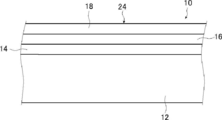
- FIG. 1 is a cross-sectional view schematically showing an example of the specific transfer film.
- the transfer film 10 comprises a support 12, a protective layer 14 formed on one surface of the support 12, a receptive layer 16 formed on the surface of the protective layer 14, and a receptive layer 16 And a solvent permeation layer 18 formed on the surface of
- the solvent permeation layer 18 is adhered to the substrate P, and then the support 12 is a protective layer
- the laminate including the solvent permeation layer 18, the receiving layer 16 and the protective layer 14 is transferred to the substrate P, and a wiring pattern is formed on the substrate P. Therefore, in a state in which the laminate including the solvent permeation layer 18, the receiving layer 16 and the protective layer 14 is transferred to the substrate P, the protective layer 14 becomes the surface and the solvent permeation layer 18 becomes the substrate P side.
- the support 12 supports the protective layer 14, the receptive layer 16 and the solvent permeation layer 18 until the transfer film 10 is adhered to the substrate P.
- the support 12 various known sheet materials (films) capable of supporting the protective layer 14, the receptive layer 16 and the solvent permeation layer 18 can be used.
- the sticking step described later is carried out under heating (that is, in the case of heat sticking)
- the support 12 having sufficient heat resistance.
- Specific examples of the support 12 include resin films formed of various resin materials.
- Specific examples of the resin material to be the support 12 include polyester resins such as polyethylene terephthalate (PET (polyethylene terephthalate)) and polyethylene naphthalate (PEN (polyethylene naphthalate)), polycarbonate resins, acrylic resins, methacrylic resins, and And polyimide resins.
- the thickness of the support 12 is not particularly limited, but the protective layer 14, the receptive layer 16 and the solvent permeation layer 18 can be supported until the adhesion process described later is performed, and the transfer film 10 is adhered to the substrate P After that, a thickness that can be properly peeled without causing breakage or the like may be appropriately set according to the forming material or the like.
- the thickness of the support 12 is preferably 20 to 200 ⁇ m, and more preferably 50 to 130 ⁇ m.
- Protective layer 14 is formed on one surface of support 12.
- the protective layer 14 is a layer that protects the receptive layer 16 after the peeling process described later.
- the protective layer 14 preferably comprises a polymer. 0 degreeC or more is preferable, as for the glass transition temperature (Tg) of the polymer which may be contained in the protective layer 14, 20 degreeC or more is more preferable, and 30 degreeC or more is more preferable.
- Tg glass transition temperature
- the upper limit of the Tg of the polymer that can be contained in the protective layer 14 is preferably 80 ° C. or less. If the Tg of the above-mentioned polymer is 80 ° C.
- the protective layer 14 can be favorably formed (film-formed), and since the film-forming temperature can be lowered, the selection range of the support 12 can be expanded.
- the Tg of the polymer may be measured by a known method, or the numerical values described in various documents may be used, and when using a commercially available polymer, the numerical values described in the catalog etc. Or a numerical value calculated from the composition of the polymer.
- the measuring method of glass transition temperature the method of measuring based on JIS (Japanese Industrial Standards) K7121 by a differential scanning calorimetry is mentioned.
- the solubility parameter (SP value) of the polymer that can be contained in the protective layer 14 is preferably 8.5 (cal / cm 3 ) 1/2 or more, and more preferably 9.0 (cal / cm 3 ) 1/2 or more.
- the protective layer 14 can be formed of a polymer having high polarity and strong molecular cohesion, so that the scratch resistance of the protective layer 14 becomes good.
- there are advantages such as high tensile strength of the protective layer 14 and good peelability.
- the solubility parameter of the polymer may be measured by a known method, or the numerical values described in various documents may be used, and in the case of using a commercially available polymer, it is described in a catalog etc. You may use a numerical value.
- the formation of the wiring pattern on the substrate P using the transfer film 10 is carried out by adhering the solvent permeation layer 18 and the substrate P in a state where the solvent permeation layer 18 and the substrate P are in contact with each other as described above , By peeling the support 12.
- the lower limit of the thickness of the protective layer 14 is not particularly limited, and a thickness that can sufficiently protect the receiving layer 16 may be appropriately set according to the material of the protective layer 14.
- the thickness of the protective layer 14 is preferably 1 ⁇ m or more, and more preferably 2 ⁇ m or more.
- the protective layer 14 may have a single-layer structure or a multi-layer structure.
- polymers that can be included in the protective layer 14 various known polymers can be used.
- urethane based polymer acrylic based polymer, vinyl acetate based polymer, polyvinyl chloride based polymer, rubber based polymer, styrene based polymer, silicone based polymer, ester based polymer, amide based polymer, and repeating units constituting these polymers
- the copolymer which contains multiple types is mentioned.
- urethane polymers are preferable in that the releasability of the support 12 is more excellent.
- the polymer which may be contained in the protective layer 14 may use a commercial item.
- specific examples of the polymer having a Tg of 0 ° C. or higher include Superflex 170 (urethane-based polymer), Superflex 820 (urethane-based polymer), Superflex 830HS (urethane-based polymer) manufactured by Daiichi Kogyo Seiyaku Co., Ltd.
- the protective layer 14 may contain two or more types of polymers, and it is preferable that the Tg of each of the two or more types of polymers is 0 ° C. or more.
- the protective layer 14 contains 2 or more types of polymers, the characteristic of each polymer is expressed, and the transfer film 10 which is excellent in transferability and the flaw resistance of a protective layer is obtained.
- a urethane polymer and an ethylene-vinyl acetate-vinyl chloride copolymer are used in combination, a transfer film 10 excellent in the peelability of the support 12 and the scratch resistance of the protective layer 14 can be obtained.
- the content of the polymer having a Tg of 0 ° C. or more is preferably 20% by mass or more, more preferably 30% by mass or more, and still more preferably 50% by mass or more based on the total mass of the protective layer 14. If the content of the polymer having a Tg of 0 ° C. or more is 20% by mass or more, the releasability between the support 12 and the protective layer 14 becomes good, the scratch resistance of the protective layer 14 becomes good, It is preferable from the point that bendability (flexibility) becomes good.
- the protective layer 14 may contain a surfactant. If the protective layer 14 contains a surfactant, the releasability between the support 12 and the protective layer 14 can be improved.
- the surfactant can use the well-known surfactant according to the formation material of the protective layer 14. Specific examples of the surfactant include ethers such as polyoxyethylene nonyl phenyl ether, polyoxyethylene octyl phenyl ether, polyoxyethylene dodecyl phenyl ether, polyoxyethylene oleyl ether, polyoxyethylene lauryl ether, polyoxyethylene alkyl ether, etc.
- Emulgen series such as Kao Corp.'s Emulgen 108, 109 P, etc., Nippon Tanso Co., Ltd. Softanol EP-5035, 7085, 9050, Adeka's Pluronic L-31, L-34, L-44 etc.
- Esters such as polyoxyethylene oleate, polyoxyethylene distearate, sorbitan laurate, sorbitan monostearate, sorbitan monooleate, sorbitan sesquioleate, polyoxyethylene monooleate, polyoxyethylene stearate and the like; Polyoxyethylene acetylene glycol ether, polyoxyethylene distyrenated phenyl ether, polyoxyethylene tribenzylated phenyl ether, etc.
- Nonionic surfactants such as 485, olfine STG, etc .; polyglycol ethers; etc. may be mentioned.
- the content of the surfactant is preferably 0.01 to 5% by mass, and more preferably 0.1 to 2% by mass, with respect to the total mass of the protective layer 14.
- the protective layer 14 may contain components other than the above as required, and examples thereof include various additives such as waxes, inorganic pigments, ultraviolet absorbers, and antioxidants.
- the receptive layer 16 is formed on the surface of the protective layer 14.
- the receiving layer 16 is a layer that receives a solvent (water and / or an organic solvent) contained in the conductive ink. Specifically, the receptive layer 16 penetrates the solvent permeation layer 18 and mainly accepts the solvent contained in the conductive ink that has passed through the solvent permeation layer 18.
- the receptive layer 16 is not limited to the solvent contained in the conductive ink, but may be a component (a liquid or a solid which has passed through the solvent permeation layer 18). For example, conductive materials and coloring materials may be mentioned. Can be accepted.
- the receiving layer 16 is a layer formed using a polymer that receives and swells a solvent, or voids (fine particles) in which fine particles insoluble in the solvent (dispersion medium) contained in the conductive ink are fixed by the binder. Layers having holes).
- the transfer film 10 has the solvent permeable layer 18
- a conductive substance and necessary Accordingly, the color material etc. used is held.
- FIG. 2 conceptually shows an example of the configuration of the receiving layer 16.
- the receiving layer 16 shown in FIG. 2 is formed by fixing a plurality of receiving particles 20 insoluble in the conductive ink with a binder, and the ink is received in each gap of the receiving particles 20.
- the conductive ink contains a coloring material (described later)
- a fixing agent for fixing the coloring material in the conductive ink between the receiving particles 20 and a material that does not cause aggregation For example, nonpolar or low polar materials are used.
- the receptor particles 20 include polymer fine particles such as polyolefin, acrylic, polystyrene, and polyester, and inorganic substances such as calcium carbonate, kaolin, aluminum silicate, calcium silicate, colloidal silica, alumina, and aluminum hydroxide. There are fine particles.
- the binder for fixing the receiving particle 20 include water-soluble polymers such as gelatin, polyvinyl alcohol, polyvinyl pyrrolidone, alginic acid, aqueous polyester, and aqueous acrylic resin. Where the conductive ink comprises metal nanowires, polyvinyl pyrrolidone is preferred, which can also be stabilized with aqueous and solvent inks.
- the colorant may be received by the receiving layer 16.
- the receptive layer 16 itself has a light scattering ability, the light is scattered when the wiring pattern is built up (for example, when it is developed for the purpose of providing a backlight against the wiring substrate). Lightness and saturation may decrease. Therefore, the receptive layer 16 preferably has low light scattering ability and is transparent. Taking this point into consideration, the receptive particle 20 is colorless and the particle size is smaller than the wavelength of visible light, or the colorless receptive particle 20 in order to suppress light scattering and light absorption to make the receptive layer 16 transparent.
- refractive index difference 0.1 or less
- examples of combinations in which the refractive index difference between the receiving particles 20 and the binder is 0.1 or less include combinations using silica as the receiving particles 20 and polyvinyl alcohol (PVA (polyvinyl alcohol)) as the binder.
- PVA polyvinyl alcohol
- the thickness of the receptive layer 16 is not particularly limited, and may be appropriately set according to the material of the receptive layer 16 such as the receptive particle 20 and the like. Specifically, the thickness of the receiving layer 16 is preferably 5 to 50 ⁇ m, and more preferably 10 to 40 ⁇ m.
- the receiving layer 16 may have a single-layer structure or a multi-layer structure.
- Ink absorption capacity of the receiving layer 16 is 3 preferably ⁇ 40 mL / m 2, more preferably 6 ⁇ 30mL / m 2. The higher the ink absorption capacity of the receptive layer 16, the higher the electrical conductivity.
- the ink absorption capacity is a value obtained by the following measurement method.
- the ink jet recording medium is cut to a size of 10 cm to obtain a test piece, and 1 mL of diethylene glycol is dropped on the ink receiving layer of the obtained test strip, and then excess diethylene glycol which can not be absorbed is wiped off
- the ink absorption capacity (mL / m 2 ) is determined from the mass difference of the receptive layer and the specific gravity of diethylene glycol.
- the solvent permeable layer 18 is formed on the surface of the receptive layer.
- the solvent permeation layer 18 is a layer having a void for allowing the solvent contained in the conductive ink to permeate.
- the solvent permeation layer 18 also has a function of holding a conductive substance (for example, metal nanowires) that may be contained in the conductive ink after the transfer film 10 is printed with a wiring pattern.
- the solvent permeation layer 18 may hold, among the components contained in the conductive ink, a component that can not pass through the air gap.
- the solvent permeation layer 18 may act as an adhesive layer (adhesive layer, adhesive layer) for adhering the transfer film 10 to the substrate P after printing of the wiring pattern on the transfer film 10 is performed. .
- FIG. 3 conceptually shows the configuration of the solvent permeation layer 18.
- the voids through which the solvent contained in the conductive ink permeates are formed by the gaps L of the plurality of thermoplastic resin particles 26 dispersed and present throughout the layer.
- the gaps L formed by the thermoplastic resin particles 26 being continuous in the thickness direction, voids penetrating the solvent permeation layer 18 in the thickness direction are formed.
- the solvent contained in the conductive ink attached to the surface 24 passes the air gap penetrating in the thickness direction, whereby the solvent contained in the conductive ink passes through the solvent permeable layer 18. Is supplied to the receptive layer 16.
- the conductive substance contained in the conductive ink adheres to the surface of the thermoplastic resin particles 26 or is sandwiched in a void, and is held in the solvent permeation layer 18. Note that part of the conductive material may pass through the air gap and be supplied to the receiving layer 16.
- the particle size and particle distribution of the thermoplastic resin particles 26 are selected so as not to prevent the permeation of the conductive ink, and the gap L (interparticle distance) of the thermoplastic resin particles 26 is It is preferable to adjust to 0.1 ⁇ m or more. Further, in the solvent permeation layer 18, the particle size of the thermoplastic resin particles 26 is set to 0.degree. So that the permeation of the conductive ink is not hindered and the conductive ink does not diffuse in the direction parallel to the main surface of the transfer film 10. The thickness is preferably 1 to 10 ⁇ m.
- the thermoplastic resin particles 26 have a softening temperature of 40 to 100 ° C. so that they do not soften or coat at ambient temperature such as room temperature until the transfer film 10 is adhered to the substrate P. It is preferable to form with the following materials. Such materials include, for example, styrene copolymer resins of styrene and acrylic and butadiene, polyolefin resins, resins consisting of polymethacrylic acid and derivatives thereof, acrylic ester resins, polyacrylamide resins, polyester resins Resins and polyamide resins are mentioned.
- the tackifier particles 28 for improving the adhesion to the substrate P be dispersed and contained in the solvent permeation layer 18.
- rosin, rosin ester, alicyclic resin, phenol resin, chlorinated polyolefin resin, urethane resin, etc. can be used as materials for forming the tackifier particles 28, rosin, rosin ester, alicyclic resin, phenol resin, chlorinated polyolefin resin, urethane resin, etc. can be used.
- the tackifier may be contained in the interior of the thermoplastic resin particles 26 without being dispersed in the solvent permeation layer 18 as particles.
- heat adhesion if the tackifier is incorporated into the thermoplastic resin at the time of heat adhesion, the adhesion to the substrate P can be strengthened.
- the solvent permeation layer 18 is closer to the substrate P than the receiving layer 16 supporting the wiring substrate. That is, in the case where the conductivity of the wiring substrate formed on the substrate P is confirmed by the transfer film 10, the solvent permeation layer 18 is a base of the receiving layer 16 that holds an image. Therefore, for example, organic resin fine particles made of white inorganic pigment, white polycarbonate and / or (meth) acrylic resin, or light scattering particles are mixed into the solvent permeation layer 18 to form the solvent permeation layer 18. It may be a white layer or a light scattering layer. As a result, a wiring pattern excellent in the visibility and sharpness of the wiring pattern can be obtained, which is suitable when it is desired to clearly display the wiring substrate (wiring pattern) to which the transfer film 10 is transferred.
- the thickness of the solvent permeation layer 18 is not particularly limited, and may be a thickness that enables adhesion to the substrate P with sufficient adhesion depending on the material for forming the solvent permeation layer 18 such as the thermoplastic resin particles 26. Can be set as appropriate. Specifically, the thickness of the solvent permeation layer 18 is preferably 0.5 to 5 ⁇ m, and more preferably 0.8 to 3 ⁇ m.
- the solvent permeation layer 18 may have a single layer structure or a multilayer structure.
- the transfer film 10 can be produced by a known method according to the forming material of each layer. Hereinafter, an example of a method of manufacturing the transfer film 10 will be described.
- a resin film to be the support 12 is prepared.
- a coating solution for forming the protective layer 14 is prepared by dissolving or dispersing a compound (for example, a polymer having a Tg of 0 ° C. or more) or the like to be the protective layer 14 in ion exchanged water or the like.
- a coating solution for forming the receiving layer 16 is prepared by dissolving or dispersing the compound to be the receiving layer 16 such as the ink receiving particles 20 (for example, silica particles) and the binder in ion exchange water or the like.
- a coating liquid for forming a solvent permeation layer 18 is prepared by dissolving or dispersing a compound to be the solvent permeation layer 18 such as thermoplastic resin particles 26 (for example, polyethylene particles) and a binder in ion exchanged water or the like.
- a coating solution for forming the protective layer 14 is applied to the surface of the support 12 and dried to form the protective layer 14.
- the coating solution may be applied by a known method such as a bar coating method, a die coating method, and dipping (dip coating).
- the coating solution may also be dried by a known method suitable for the coating solution, such as hot air or heat drying using a heater.
- the receiving layer 16 and the solvent permeable layer 18 are also the same.
- a coating solution for forming the receiving layer 16 is applied to the surface of the formed protective layer 14 and dried to form the receiving layer 16.
- a coating solution for forming the solvent permeation layer 18 is applied to the surface of the formed receptor layer 16 and dried to form the solvent permeation layer 18.
- the transfer film 10 is obtained.
- substrate there is no restriction
- substrate P Resin molded articles (for example, film), such as cards and various sensors, such as a wearable wiring board, Metal products, such as a silicon wafer, It forms by paper, such as a coated ball and corrugated paper.
- Various known articles such as products are available.
- polyester-based resin such as a polyethylene terephthalate (PET (polyethylene terephthalate)) and a polyethylene naphthalate (PEN (polyethylene naphthalate)
- PET polyethylene terephthalate
- PEN polyethylene naphthalate
- a polycarbonate resin an acrylic resin, a methacryl resin, and a polyimide Resin etc.
- the substrates P large three-dimensional objects, films with low heat resistance, papers and the like are susceptible to processes such as development, etching, and baking, and thus may not be used in the conventional method. Wiring can be formed without performing the above process. Therefore, in the present manufacturing method, as the substrate P, a large three-dimensional object, a film having low heat resistance, paper and the like can also be suitably used.
- the conductive ink in the present invention contains a conductive substance and a solvent. Conductivity means passing electricity.
- the conductive material is not particularly limited as long as it has conductivity, and, for example, metals such as copper, chromium, lead, nickel, gold, platinum, palladium, silver, tin, and zinc, and metals thereof Alloys of The conductive substance may be in any shape such as a sphere or a wire, but a wire is preferable from the viewpoint of more excellent conductivity, and a wire or a metal nano composed of a metal alloy (ie, metal nano) It is preferable that it is a wire.
- the metal nanowires are preferably made of silver and metals other than silver.
- metals other than silver metals nobler than silver are preferable, gold, platinum and palladium are more preferable, and gold is more preferable.
- Metals other than silver may be alloyed with silver and may be coated with silver nanowires to be the core, but it is preferable to coat silver nanowires. When the silver nanowires are coated, the metal other than silver does not necessarily have to cover the entire surface of the core silver nanowires, and may be partially coated.
- the metals nobler than silver are introduced by alloying silver nanowires with this or plating on the surface because the ionization energy is higher than silver. This can improve the oxidation resistance of the metal nanowires.
- a metal nobler than silver specifically, 0.5 to 10 parts by mass with respect to 100 parts by mass of silver is preferable, and 1 to 5 parts by mass is more preferable
- the heat resistance of the nanowire can be improved.
- the content of each metal atom in the metal nanowire can be measured, for example, by dissolving the metal nanowire with an acid or the like and then using an ICP (high frequency inductively coupled plasma) emission spectrometer.
- the major axis average length of the metal nanowires is preferably 1 ⁇ m or more, more preferably 5 ⁇ m or more, and still more preferably 10 ⁇ m or more, from the viewpoint of easy conduction and low resistance of the wiring pattern.
- the upper limit value of the long axis average length of the metal nanowires is 1000 ⁇ m or less from the viewpoint of dispersion stability and ejection stability of ink jet printing.
- the average minor axis length of the metal nanowires is preferably 3 nm or more and less than 200 nm, and more preferably 5 to 100 nm.
- the major axis average length of the metal nanowires can be selected by arbitrarily selecting 200 metal nanowires from a TEM image including a plurality of metal nanowires observed using a transmission electron microscope (TEM). It is a value obtained by arithmetically averaging the lengths of the major axes of the metal nanowires.
- TEM transmission electron microscope
- the average short-axis length of the metal nanowires can be selected arbitrarily from 200 metal nanowires from the TEM image including a plurality of metal nanowires, and the short-axis length of each metal nanowire can be determined. It is a value obtained by arithmetic averaging.
- the aspect ratio of the metal nanowire is preferably 200 or more.
- the upper limit of the aspect ratio of the metal nanowires is usually 10000 or less.
- the aspect ratio of metal nanowire means the ratio of the long axis average length with respect to the short axis average length in metal nanowire.
- the aspect ratio of the metal nanowires and the content of the metal other than silver are the concentrations of metal salts, inorganic salts and organic acids (or salts thereof), solvent species during particle formation, reduction in the method of producing metal nanowires
- concentration can be controlled by appropriately selecting the concentration of the agent, the addition rate of each component, the temperature and the like.
- the methods described in paragraphs 0019 to 0024 of JP-A-2011-149092 can be mentioned.
- the content of the conductive substance is preferably 0.1 to 20% by mass, and more preferably 0.3 to 15% by mass, with respect to the total mass of the conductive ink.
- the heat resistance of the metal nanowire it is considered preferable to have the following heat resistance.
- a wiring pattern (wiring substrate) formed using metal nanowires is used for various device applications, bonding (paneling) with a thermoplastic resin generally at 150 ° C. or higher in manufacturing processes of various devices
- the heat resistance which can endure the process and the solder reflow process of a 220 degreeC or more wiring part is required.
- the silver nanowires When heated, the silver nanowires deform so as to approximate a spherical shape in order to minimize the surface area. Specifically, there is a possibility that the wire may be broken and the pieces may be deformed so as to approach a spherical shape, respectively.
- the resistance value When exposed to heat and a high humidity environment for a long time, the resistance value is increased and finally the conduction is removed. It may disappear.
- a strong insulating layer is formed on the surface of the wiring substrate after the peeling step by using the bonding step and the peeling step in combination in the present manufacturing method. Even when exposed to an environment of 85 ° C. and 85% RH (relative humidity) for 120 hours, it is possible to suppress the fluctuation of the resistance value.
- the solvent has a function of, for example, dispersing or dissolving components contained in the conductive ink, and adjusting the viscosity of the conductive ink.
- Solvents include water and organic solvents. Either water or an organic solvent may be used alone, or both may be used in combination. When water and an organic solvent are used in combination, it is preferable to use an organic solvent miscible with water.
- the organic solvent is not limited thereto, but alcohol solvents having a normal boiling point of 50 ° C. to 250 ° C. are preferable, and alcohol solvents having a standard boiling point of 55 ° C. to 200 ° C. are more preferable. When an alcohol solvent having a standard boiling point of 50 ° C. to 250 ° C. is used, there is an advantage that discharge stability is improved and the drying speed of the conductive ink is improved when printing is performed by the inkjet method.
- an alcohol type compound there is no restriction
- the alcohol compounds may be used alone or in combination of two or more.
- organic solvents it is preferable to include an organic solvent having a boiling point of 100 ° C. or more from the viewpoint of suppressing discharge failure caused by drying of the conductive ink in the discharge head of the ink jet recording apparatus.
- the content of the organic solvent having a boiling point of 100 ° C. is preferably 5 to 30, and more preferably 8 to 25% by mass with respect to the total mass of the conductive ink.
- the conductive ink preferably contains a compound represented by the following formula (I) (hereinafter, also referred to as “compound (I)”).
- Compound (I) is also called noble metal thioglucose.
- migration means that a conductive substance such as metal is ionized to migrate ions (migration).
- X represents a gold atom, a palladium atom or a platinum atom, and a gold atom is preferable from the viewpoint of achieving both the stability of the wiring pattern and the conductivity.
- metal nanowires are very useful because they can exhibit conductivity even when a wiring pattern is formed at room temperature.
- metal generally has a property that the surface is oxidized, as the surface area of the nano area is increased, migration is likely to occur, and as a result, the wiring pattern may be broken.
- migration can be suppressed by using the above-mentioned compound (I), so that the occurrence of disconnection of the wiring pattern can be suppressed. Therefore, the conductive ink is preferably used in combination of the metal nanowires and the compound (I).
- the content of the compound (I) is preferably 0.005 to 0.5% by mass, more preferably 0.01 to 0.3% by mass, and more preferably 0.02 to 0. 1% by mass is more preferable. When the content of the compound (I) is in the above range, the above effect is more exhibited.
- the mass ratio of the metal nanowire to the compound (I) is preferably more than 10 and less than 1000, more preferably more than 20 and less than 150, and more than 50 and less than 120 More preferable. If the mass ratio is more than 10, the action of the sulfur atom in the molecular skeleton of the compound (I) can be suppressed, whereby the conductivity of the wiring pattern is further improved. When the mass ratio is less than 1000, the durability of the wiring board is further improved.
- the conductive ink may contain magnetic particles.
- the magnetic particles When a magnetic field is applied to the discharge head when the wiring pattern is printed by the inkjet method, the magnetic particles are arranged along the magnetic field.
- the conductive substance in particular, the metal nanowires
- the conductive substance does not easily get stuck in the discharge nozzle.
- the discharge stability of the conductive ink is improved.
- the magnetic particles include iron oxide particles composed of one or more of magnetite (Fe 3 O 4 ) and maghemite ( ⁇ -Fe 2 O 3 ).
- the content of the magnetic particles is preferably 0.1 to 20% by mass, more preferably 0.5 to 10% by mass, and still more preferably 1 to 5% by mass with respect to the total mass of the conductive ink.
- the magnetic particles may be added to the conductive ink in the form of a magnetic fluid in which the magnetic particles are dispersed in a liquid medium.
- the conductive ink may contain a colorant.
- the wiring pattern can be made to have a color corresponding to the substrate, and depiction by the wiring pattern is also possible.
- the colorant include dyes and pigments, and dyes are preferable because they are easily dissolved in a solvent and easily held by the receiving layer.
- the types of dyes and pigments are not particularly limited, and known materials may be used.
- the content of the colorant is preferably 0.02 to 10% by mass, more preferably 0.1 to 5% by mass, and still more preferably 0.2 to 3% by mass, with respect to the total mass of the conductive ink.
- the content of the coloring material is preferably 0.1 to 100 parts by mass, more preferably 1 to 50 parts by mass, and still more preferably 2 to 20% by mass with respect to 100 parts by mass of the conductive material in the conductive ink.
- the conductive ink may contain components other than the above components to such an extent that the conductivity is not affected.
- Other components include polymerizable compounds, sulfurization inhibitors, corrosion inhibitors, surfactants, antioxidants, viscosity modifiers, preservatives, and the like.
- the conductive ink preferably contains a corrosion inhibitor. By containing a corrosion inhibitor, a higher antirust effect may be exhibited.
- the corrosion inhibitor is preferably an azole, and specifically, benzotriazole, tolyltriazole, mercaptobenzothiazole, mercaptobenzotriazole, mercaptobenzotetrazole, (2-benzothiazolylthio) acetic acid, 3- (2-benzothia) Zorylthio) propionic acid, and their alkali metal salts, ammonium salts and amine salts.
- the corrosion inhibitor may be used alone or in combination of two or more.
- the corrosion inhibitor may be added dissolved in a solvent suitable for the conductive ink. When the conductive ink contains the corrosion inhibitor and the compound (I), the mass ratio of the corrosion inhibitor to the compound (I) is preferably 0.01 or less.
- the conductive ink preferably does not contain inorganic ions such as alkali metal ions, alkaline earth metal ions, and halide ions from the viewpoint of minimizing the decrease in conductivity due to metal corrosion.
- the electric conductivity of the conductive ink is preferably 1 mS / cm or less, more preferably 0.1 mS / cm or less, and still more preferably 0.05 mS / cm or less.
- the conductivity can be measured using a portable conductivity meter CM-31P (trade name, Toa DKK Co., Ltd.).
- the viscosity at 25 ° C. of the conductive ink is preferably 0.5 to 100 mPa ⁇ s, and more preferably 1 to 50 mPa ⁇ s.
- the viscosity can be measured using Viscomate VM-1G-L (trade name, manufactured by Tokyo Glass Instruments (TGK)).
- conductive ink is discharged from the nozzle of the discharge head of the ink jet recording apparatus, and droplets are deposited on the surface 24 of the solvent permeation layer 18 of the transfer film 10.
- the solvent contained in the deposited conductive ink penetrates the gap of the thermoplastic resin particles 26 to penetrate the solvent permeation layer 18 and is held by the receiving layer 16.
- the conductive substance (for example, metal nanowires) contained in the deposited conductive ink adheres to the surface of the thermoplastic resin particles 26 or is sandwiched between the thermoplastic resin particles 26 and fixed. Be done.
- the wiring pattern is held by the solvent permeation layer 18 (wiring pattern formation step).
- the solvent penetrable layer 18 of the transfer film 10 on which the wiring pattern is formed is brought into contact with the substrate P, and the transfer film 10 and the substrate P are laminated.
- the transfer film 10 (solvent permeation layer 18) and the substrate P are heat-bonded by heating from the support 12 side as necessary while pressing the transfer film 10 and the substrate P as necessary. It adheres (heat adhesion, heat adhesion) (adhesion process, refer to FIG. 4).
- 80 degreeC or more is preferable
- 90 degreeC or more is more preferable
- 100 degreeC or more is more preferable.
- the adhesion between the transfer film 10 and the substrate P is further improved by performing heat adhesion at 80 ° C. or higher.
- 150 degrees C or less is preferable, as for the lower limit of heating temperature, 140 degrees C or less is more preferable, and 130 degrees C or less is more preferable.
- the temperature is 130 ° C. or less, there is the advantage that, when the substrate P is a PET film, precipitation of low molecular weight substances (eg, oligomers) present in PET can be suppressed or deformation of the substrate P can be suppressed.
- the said temperature says the largest reach
- the support 12 is peeled off from the transfer film 10 stuck to the substrate P.
- the wiring substrate 100 is formed by transferring the laminated body in which the solvent permeation layer 18, the receiving layer 16, and the protective layer 14 in which the wiring pattern is formed is sequentially laminated onto the substrate P. Obtained (peeling step, see FIG. 5).
- the wiring pattern is photo-sintered to reduce the resistance of the wiring pattern.
- the exposure is not particularly limited as long as it is after the wiring pattern formation step, but is preferably performed before the peeling step.
- the exposure is performed, for example, by irradiation with ultraviolet light using a trade name “PulseForge 3300” manufactured by Novacentrix.
- the exposure conditions may be implemented according to known conditions to the extent that deformation of the transfer film 10 does not occur.
- the irradiation energy is preferably 1 to 20 J / cm 2
- the pulse irradiation time is preferably 10 to 10000 ⁇ sec
- the number of times of irradiation is preferably 5 to 30 times.
- this manufacturing method may manufacture the wiring substrate 100 using a cut sheet-like transfer film as shown in FIGS. 4 and 5, the transfer film and the substrate using a long transfer film
- the transfer film may be attached to the substrate while moving the transfer film in the longitudinal direction of the transfer film at the same speed to manufacture the wiring substrate.
- FIGS. 4 and 5 show an example of manufacturing the wiring substrate 100 in which one set of laminates (the solvent permeation layer 18, the receiving layer 16, the protective layer 14 on which the wiring pattern is formed) is stacked on the substrate P.
- a wiring board (multilayer wiring board) in which two or more sets of laminates are stacked on the substrate P may be manufactured. That is, as another embodiment of the present manufacturing method, a new transfer film having a wiring pattern obtained in the above wiring pattern forming step is attached on the wiring substrate obtained in the above peeling step, The method of peeling a support body in a new transfer film may be repeated to obtain a wiring substrate such that a plurality of wiring patterns are stacked on the substrate. Thereby, a wiring board (multilayer wiring board) in which a plurality of wiring patterns are stacked on the substrate can be obtained.
- a new transfer film X1 on which a wiring pattern is formed which is obtained by the above-described wiring pattern formation process, is prepared (preparation process).
- the transfer film X1 is formed by sequentially laminating a protective layer 14A, a receiving layer 16A, and a solvent permeation layer 18A in which a wiring pattern is formed on one surface of a support 12A.
- the solvent permeable layer 18A of the transfer film X1 is brought into contact with the protective layer 14 of the wiring substrate 100 obtained by the peeling process described in FIG. 5 to bond the transfer film X1 and the wiring substrate 100 (transfer Sticking process of film X1, see FIG. 6).
- the support 12A is peeled off from the transfer film X1 (peeling process using the transfer film X1, see FIG. 7).
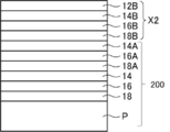
- the wiring board 200 in which two laminates each having a wiring pattern are stacked on the substrate P can be obtained.
- the transfer film X2 is formed by sequentially laminating a protective layer 14B, a receiving layer 16B, and a solvent permeation layer 18B in which a wiring pattern is formed on one surface of a support 12B.
- the solvent permeable layer 18B of the transfer film X2 is brought into contact with the protective layer 14A of the wiring substrate 200, and the transfer film X2 and the wiring substrate 200 are attached (transfer film Sticking process using X2, see FIG. 8).
- the support 12B is peeled off from the transfer film X2 (peeling process using the transfer film X2, see FIG. 9).
- the wiring board 300 in which three laminates each having a wiring pattern are stacked on the substrate P is obtained.
- the wiring board obtained by the present manufacturing method holds the security of card materials such as, for example, riding cards such as trains and buses, credit cards, electronic money cards, identification (ID) cards, card keys, various point cards, etc. It is suitably used for forming an electronic circuit, a complex radio frequency (RF) chip for enhancing confidentiality of various information, and an antenna circuit for energy harvesting.
- the wiring substrate is preferably a thin film.
- the stirring speed was changed to 100 rpm, and the temperature was maintained at 135 ° C. for 3.0 hours to complete heating, and natural cooling was continued until the temperature reached 80 ° C. or less.
- a part of the solution (slurry after reaction) was separated into a centrifuge tube, washed by adding distilled water, and centrifuged at 3000 rpm for 5 minutes. After removing the supernatant after centrifugation, methanol was added to wash the precipitate, and the methanol dispersion was centrifuged at 2500 rpm for 5 minutes.
- the major axis average length and the minor axis average length are calculated using a transmission electron microscope (TEM), and the aspect ratio (major axis average length is calculated based on the obtained values. / Short axis average length) was calculated. Each value is shown in Table 1.
- [Production of conductive ink] 20 ml of ethylene glycol and 5 ml of ethanol were added to 75 ml of the dispersion of silver nanowire (A) to prepare a conductive ink 1. After preparation, ultrasonic dispersion was carried out for 20 minutes, and then stirring was carried out at 2500 rpm for 20 minutes using “T 18 digital ULTRA-TURRAX” (trade name) manufactured by IKA Corporation to complete redispersion.
- the viscosity of the conductive ink 1 was 15 mPa ⁇ s (25 ° C.) or less. The viscosity was measured by "VISCOMATE VM-1G" (trade name) manufactured by CBC Materials.
- [Conductive ink 2] In 75 ml of a dispersion of silver nanowire (A), 20 mg of ethylene glycol and 15 mg of a compound represented by the following formula (I-1) (gold thioglucose) are dissolved in 5 ml of ethanol to prepare metal nano for gold thioglucose.
- the conductive ink 2 was prepared by adding the mass ratio of the wire to 100. The other operations were the same as in the case of the conductive ink 1 to obtain a conductive ink 2.
- the viscosity of the conductive ink 2 was 15 mPa ⁇ s (25 ° C.) or less (measured under the same conditions as the conductive ink 1).
- a conductive ink 3 was obtained in the same manner as the conductive ink 2 except that the dispersion of silver nanowires (B) was used instead of the dispersion of silver nanowires (A).
- the viscosity of the conductive ink 3 was 17 mPa ⁇ s (25 ° C.) or less (measured under the same conditions as the conductive ink 1).
- a conductive ink 4 was obtained in the same manner as the conductive ink 2 except that the dispersion of the silver nanowire (C) was used instead of the dispersion of the silver nanowire (A).
- the viscosity of the conductive ink 4 was 17 mPa ⁇ s (25 ° C.) or less (measured under the same conditions as the conductive ink 1).
- a conductive ink 5 was obtained in the same manner as the conductive ink 2 except that 1.5 g of solid magnetic fluid (MSG-W11, manufactured by FeroTec) was added.
- MSG-W11 is an aqueous liquid medium in which magnetic particles (mixture of magnetite (Fe 3 O 4 ) particles and maghemite ( ⁇ -Fe 2 O 3 ) particles) are dispersed, and the average particle diameter is 10 nm. It is.
- the viscosity of the conductive ink 5 was 17 mPa ⁇ s (25 ° C.) or less (measured under the same conditions as the conductive ink 1).
- Conductive ink 6 Silver nanoparticle ink (trade name “NBSIJ-MU01”) manufactured by Mitsubishi Paper Industries, Ltd. was used as the conductive ink 6. The viscosity of the conductive ink 6 was 2.3 mPa ⁇ s (25 ° C.) or less (measured under the same conditions as the conductive ink 1).
- a conductive ink 7 is used in the same manner as the conductive ink 2 except that a compound represented by the following formula (II) is used instead of the compound (gold thioglucose) represented by the above formula (I-1). I got The viscosity of the conductive ink 7 was 17 mPa ⁇ s (25 ° C.) or less (measured under the same conditions as the conductive ink 1).
- a conductive ink 8 is obtained in the same manner as the conductive ink 2 except that the weight ratio of the metal nanowire to the compound (gold thioglucose) represented by the above formula (I-1) is 11
- the viscosity of the conductive ink 8 was 17 mPa ⁇ s (25 ° C.) or less (measured under the same conditions as the conductive ink 1).
- a conductive ink 9 is obtained in the same manner as the conductive ink 2 except that the mass ratio of the metal nanowire to the compound (gold thioglucose) represented by the above formula (I-1) is 999.
- the viscosity of the conductive ink 9 was 17 mPa ⁇ s (25 ° C.) or less (measured under the same conditions as the conductive ink 1).
- Transfer film A was produced as follows.
- a PET film having a width of 1000 mm, a thickness of 100 ⁇ m, and a length of 100 m (trade name “Cosmo Shine A4100” manufactured by Toyobo Co., Ltd.) was used.
- a coating solution for forming a protective layer is coated at 35 g / m 2 on a highly smooth surface of the support 12 using a # 20 wire bar, and dried at 100 ° C. for 2 minutes.
- the protective layer 14 was formed on the surface.
- the thickness of the formed protective layer 14 was 3 ⁇ m.
- the coating liquid for forming the receiving layer and the inline liquid were inline mixed and applied to the surface of the protective layer 14 previously formed, using an extrusion die coater. Specifically, the receiving layer 90.5 g / m 2 coating solution for forming a (coating amount), and line mixing inline solution 7.4 g / m 2 (coated amount) was applied.
- the formed coating layer (coating film) was dried at 80 ° C. (wind speed 5 m / sec) by a hot air dryer until the solid content concentration became 36 mass%. During this time, the coated layer showed constant drying.
- the coating layer is immersed for 3 seconds in a solution containing a basic compound, and a solution containing a basic compound is applied onto the coating layer with a solid content concentration of 36% by mass. 13 g / m 2 was attached. Furthermore, it dried at 72 degreeC for 10 minutes, and formed the receptive layer 16 in the surface of the protective layer 14. The thickness of the formed receiving layer 16 was 20 ⁇ m.
- a coating solution for forming a solvent-permeable layer is applied to the surface of the receptor layer 16 previously formed using a # 8 wire bar, and dried at 40 ° C. for 10 minutes.
- the solvent permeation layer 18 was formed to prepare a transfer film 10.
- a transfer film is formed in the same manner as in the production of the transfer film A, except that the receiving layer 16 formed using the following materials is formed instead of the receiving layer 16 of the transfer film A and the solvent permeation layer 18 is not formed.
- the receiving layer of the transfer film B was formed as follows. First, an inkjet receptive layer resin (trade name "NS-310X” manufactured by Takamatsu Yushi Co., Ltd., a swelling type receptive layer) was prepared. Next, the surface of the protective layer 14 was coated with the above-mentioned ink jet receiving layer resin at a coating amount of 70 g / m 2 using an extrusion die coater. Thereafter, it was dried at 120 ° C. for 5 minutes to form the receptive layer 16 on the surface of the protective layer 14. The thickness of the obtained receptive layer 16 was 9 ⁇ m.
- Example 1 First, using an inkjet recording apparatus, transfer film is printed by using the conductive ink 1 from the side opposite to the side on which the support 12 is formed in the transfer film A (that is, the solvent permeation layer 18). A wiring pattern was formed on 10 (wiring pattern formation step). Next, the surface on the opposite side to the surface on which the support 12 is formed in the transfer film 10 on which the wiring pattern is formed (that is, the solvent permeation layer 18) is brought into contact with the substrate P, and the transfer film 10 and the substrate P Stacked. Next, the transfer film 10 and the substrate P were pressed and heated from the side of the support 12 to thermally bond the transfer film 10 (solvent permeation layer 18) and the substrate P (adhesion step). In addition, the heating temperature of the transfer film 10 at the time of sticking was 120 degreeC. Next, the support 12 was peeled off from the transfer film 10 attached to the substrate P (peeling step). Thus, the wiring board in Example 1 was manufactured.
- Example 2 to 6 Wiring boards in Examples 2 to 6 were manufactured in the same manner as Example 1 except that conductive inks 2 to 6 were used instead of the conductive ink 1, respectively. However, in Example 5, the conductive ink 5 was discharged while applying a magnetic field so that the magnetic particles were arranged in the discharge direction of the discharge head of the ink jet recording apparatus.
- Example 7 The wiring board in Example 7 is manufactured in the same manner as in Example 6 except that the wiring pattern is exposed to UV (ultraviolet) radiation using PulseForge 3300 (trade name, manufactured by Novacentrix) before the transfer step. did. As the exposure conditions, 3 J / cm 2 of Pulse light (1400 ⁇ Sec) was irradiated 10 times.
- Example 8 The wiring board in Example 8 is manufactured in the same manner as in Example 2 except that the wiring pattern is exposed to UV (ultraviolet) irradiation using PulseForge 3300 (trade name, manufactured by Novacentrix) before the transfer step. did. As the exposure conditions, 3 J / cm 2 of Pulse light (1400 ⁇ Sec) was irradiated 10 times.
- Example 9 A wiring board in Example 9 was manufactured in the same manner as Example 2 except that transfer film B was used instead of transfer film A.
- transfer film B was used instead of transfer film A.
- the wiring pattern forming step using the transfer film B printing using the conductive ink 1 from the side of the transfer film B opposite to the side on which the support 12 is formed (that is, the receiving layer 16) Did.
- the surface (that is, the receiving layer 16) opposite to the surface on which the support 12 is formed in the transfer film 10 on which the wiring pattern is formed is brought into contact with the substrate P.
- the resistance value of the wiring board in each example was measured. Specifically, the discharge amount is set so that the amount of silver in the conductive ink to be applied is 1.5 g / m 2, and the wiring substrate in each example having a wiring pattern of width 5 mm ⁇ length 50 mm is manufactured. The resistance values at both ends of the wiring board were measured using a digital multimeter RD701 (trade name, manufactured by Sanwa Electric Instruments Co., Ltd.).
- the durability of the wiring board in each example was evaluated. Specifically, first, the discharge amount is set so that the silver amount in the conductive ink to be applied is 1.5 g / m 2, and the wiring substrate in each example having a wiring pattern of 5 mm wide ⁇ 50 mm long is used. Manufactured. The obtained wiring board was stored for 5 days under conditions of 85 ° C. and 85% RH. The resistance value of the wiring board before and after storage was measured by a digital multimeter RD701 (trade name, manufactured by Sanwa Electric Instruments Co., Ltd.). Assuming that the resistance before storage is R0 and the resistance after storage is R, the rate of change in resistance before and after storage was calculated according to the following equation.
- Example 1 In the manufacturing method of the wiring board in an example, it printed on the specific transfer film in which the protective layer was formed beforehand. Therefore, the process of forming a protective layer was unnecessary between the wiring pattern formation process and the adhesion process, and the process from printing to adhesion could be smoothly performed.
- Example 2 Example 11, and Example 12
- Example 12 when a conductive ink containing the compound represented by Formula (I-1) is used (Example 2, Example 11, and Example) Example 12) showed that the durability of the wiring board is excellent.
- Example 2 to 4 when the aspect ratio of the conductive substance (silver nanowire) is 200 or more (Examples 2 and 4), the wiring having a low resistance value and a wiring excellent in conductivity A substrate was shown to be obtained.
- Example 2 it was shown that when the conductive ink containing magnetic particles is used (Example 5), the ejection suitability of the ink jet recording apparatus is excellent. Further, from the comparison between Example 1 and Example 6, it was shown that when the metal nanowires were used (Example 1), the resistance value of the wiring pattern was low and the durability of the wiring board was also excellent. Also, from the comparison between Example 6 and Example 7 and the comparison between Example 2 and Example 8, when the exposure of the wiring pattern is carried out (Example 7 and Example 8), the resistance value of the wiring pattern is It was shown to go low.
- Example 2 From the comparison between Example 2 and Example 9, it was shown that the resistance value of the wiring pattern is lowered when the transfer film A having the receiving layer containing the receiving particles is used (Example 2). Further, from the comparison between Example 2 and Example 10, when the compound represented by the formula (I-1) is used as the migration inhibitor (Example 2), the durability of the wiring board is more excellent, and the wiring The resistance of the pattern was also shown to be low.
- a conductive ink 6 was prepared in the same manner as the conductive ink 1 except that 1 g of a dye (Direct Blue 87) was added to the conductive ink 1.
- a dye Direct Blue 87
- the evaluations of the ejection stability, the resistance value and the durability were all the same as in Example 1.
- the wiring board was visually confirmed, the colored wiring pattern was able to be confirmed.
Landscapes
- Engineering & Computer Science (AREA)
- Chemical & Material Sciences (AREA)
- Manufacturing & Machinery (AREA)
- Microelectronics & Electronic Packaging (AREA)
- Materials Engineering (AREA)
- Organic Chemistry (AREA)
- Wood Science & Technology (AREA)
- Life Sciences & Earth Sciences (AREA)
- Nanotechnology (AREA)
- Dispersion Chemistry (AREA)
- Manufacturing Of Printed Wiring (AREA)
- Inks, Pencil-Leads, Or Crayons (AREA)
- Conductive Materials (AREA)
- Parts Printed On Printed Circuit Boards (AREA)
Abstract
La présente invention vise à proposer un procédé de production de cartes de circuit imprimé qui permette de produire de manière pratique une carte de circuit imprimé, et une encre conductrice. Ledit procédé de production de cartes de circuit imprimé utilise un film de transfert qui présente ; un corps de support ; une couche de protection qui est formée sur une surface du corps de support et peut être retirée du corps de support ; et une couche de réception qui est formée sur la surface de la couche de protection et reçoit le solvant d'une encre conductrice qui contient le solvant et une substance conductrice. Le procédé de production comprend les étapes suivantes : une étape consistant à former un tracé conducteur sur le film de transfert au moyen de l'encre conductrice pour réaliser l'impression sur une surface du film de transfert qui se trouve sur la face opposée à la surface sur laquelle le corps de support est formé ; une étape de liaison qui suit l'étape de formation du tracé conducteur et qui consiste à mettre la surface sur laquelle le tracé conducteur a été formé, c'est-à-dire la surface du film de transfert qui se trouve sur la face opposée à la surface sur laquelle le corps de support est formé, en contact avec un substrat, et à lier le film de transfert et le substrat ; et une étape d'enlèvement qui suit l'étape de liaison et qui consiste à obtenir une carte de circuit imprimé en enlevant le corps de support du film de transfert qui a été lié au substrat.
Priority Applications (3)
| Application Number | Priority Date | Filing Date | Title |
|---|---|---|---|
| JP2019525334A JPWO2018235590A1 (ja) | 2017-06-23 | 2018-06-05 | 配線基板の製造方法および導電性インク |
| CN201880037159.7A CN110754140A (zh) | 2017-06-23 | 2018-06-05 | 配线基板的制造方法及导电性墨液 |
| US16/701,159 US20200107451A1 (en) | 2017-06-23 | 2019-12-03 | Method of producing wiring board and conductive ink |
Applications Claiming Priority (2)
| Application Number | Priority Date | Filing Date | Title |
|---|---|---|---|
| JP2017123286 | 2017-06-23 | ||
| JP2017-123286 | 2017-06-23 |
Related Child Applications (1)
| Application Number | Title | Priority Date | Filing Date |
|---|---|---|---|
| US16/701,159 Continuation US20200107451A1 (en) | 2017-06-23 | 2019-12-03 | Method of producing wiring board and conductive ink |
Publications (1)
| Publication Number | Publication Date |
|---|---|
| WO2018235590A1 true WO2018235590A1 (fr) | 2018-12-27 |
Family
ID=64735920
Family Applications (1)
| Application Number | Title | Priority Date | Filing Date |
|---|---|---|---|
| PCT/JP2018/021514 Ceased WO2018235590A1 (fr) | 2017-06-23 | 2018-06-05 | Procédé de production de cartes de circuit imprimé et encre conductrice |
Country Status (4)
| Country | Link |
|---|---|
| US (1) | US20200107451A1 (fr) |
| JP (1) | JPWO2018235590A1 (fr) |
| CN (1) | CN110754140A (fr) |
| WO (1) | WO2018235590A1 (fr) |
Cited By (1)
| Publication number | Priority date | Publication date | Assignee | Title |
|---|---|---|---|---|
| US20220089895A1 (en) * | 2019-02-19 | 2022-03-24 | Xtpl S.A. | Conductive ink compositions |
Families Citing this family (1)
| Publication number | Priority date | Publication date | Assignee | Title |
|---|---|---|---|---|
| CN111885841B (zh) * | 2020-07-31 | 2023-04-07 | 西安工程大学 | 一种柔性可拉伸导电线路的制备方法 |
Citations (7)
| Publication number | Priority date | Publication date | Assignee | Title |
|---|---|---|---|---|
| JP2004006578A (ja) * | 2002-04-15 | 2004-01-08 | Seiko Epson Corp | 導電膜パターンとその形成方法、配線基板、電子デバイス、電子機器、並びに非接触型カード媒体 |
| JP2006335995A (ja) * | 2005-06-06 | 2006-12-14 | Hitachi Maxell Ltd | インクジェット用導電性インク、導電性パターンおよび導電体 |
| JP2011065944A (ja) * | 2009-09-18 | 2011-03-31 | Fujifilm Corp | 導電膜形成用感光材料、導電性材料、表示素子及び太陽電池 |
| WO2013018253A1 (fr) * | 2011-07-29 | 2013-02-07 | パナソニック株式会社 | Composition d'encre photosensible de blindage électromagnétique, matériau de blindage électromagnétique durci et procédé de fabrication de matériau de blindage électromagnétique durci |
| JP2016127257A (ja) * | 2015-01-08 | 2016-07-11 | 東友ファインケム株式会社Dongwoo Fine−Chem Co., Ltd. | 柔軟基板の製造方法 |
| JP2016135919A (ja) * | 2015-01-15 | 2016-07-28 | 公立大学法人 滋賀県立大学 | 銀ナノワイヤおよびその製造方法並びにインク |
| JP2016139686A (ja) * | 2015-01-27 | 2016-08-04 | 株式会社コムラテック | 電子回路基板およびその製造方法 |
-
2018
- 2018-06-05 JP JP2019525334A patent/JPWO2018235590A1/ja not_active Abandoned
- 2018-06-05 WO PCT/JP2018/021514 patent/WO2018235590A1/fr not_active Ceased
- 2018-06-05 CN CN201880037159.7A patent/CN110754140A/zh active Pending
-
2019
- 2019-12-03 US US16/701,159 patent/US20200107451A1/en not_active Abandoned
Patent Citations (7)
| Publication number | Priority date | Publication date | Assignee | Title |
|---|---|---|---|---|
| JP2004006578A (ja) * | 2002-04-15 | 2004-01-08 | Seiko Epson Corp | 導電膜パターンとその形成方法、配線基板、電子デバイス、電子機器、並びに非接触型カード媒体 |
| JP2006335995A (ja) * | 2005-06-06 | 2006-12-14 | Hitachi Maxell Ltd | インクジェット用導電性インク、導電性パターンおよび導電体 |
| JP2011065944A (ja) * | 2009-09-18 | 2011-03-31 | Fujifilm Corp | 導電膜形成用感光材料、導電性材料、表示素子及び太陽電池 |
| WO2013018253A1 (fr) * | 2011-07-29 | 2013-02-07 | パナソニック株式会社 | Composition d'encre photosensible de blindage électromagnétique, matériau de blindage électromagnétique durci et procédé de fabrication de matériau de blindage électromagnétique durci |
| JP2016127257A (ja) * | 2015-01-08 | 2016-07-11 | 東友ファインケム株式会社Dongwoo Fine−Chem Co., Ltd. | 柔軟基板の製造方法 |
| JP2016135919A (ja) * | 2015-01-15 | 2016-07-28 | 公立大学法人 滋賀県立大学 | 銀ナノワイヤおよびその製造方法並びにインク |
| JP2016139686A (ja) * | 2015-01-27 | 2016-08-04 | 株式会社コムラテック | 電子回路基板およびその製造方法 |
Cited By (1)
| Publication number | Priority date | Publication date | Assignee | Title |
|---|---|---|---|---|
| US20220089895A1 (en) * | 2019-02-19 | 2022-03-24 | Xtpl S.A. | Conductive ink compositions |
Also Published As
| Publication number | Publication date |
|---|---|
| JPWO2018235590A1 (ja) | 2020-04-09 |
| CN110754140A (zh) | 2020-02-04 |
| US20200107451A1 (en) | 2020-04-02 |
Similar Documents
| Publication | Publication Date | Title |
|---|---|---|
| EP2347032B1 (fr) | Procédé pour réduire des films minces sur des substrats à basse température | |
| EP3028126B1 (fr) | Fixation de composants électroniques à des conducteurs imprimés transparents à base de nanofils | |
| JP5258150B2 (ja) | インク組成物 | |
| KR102035147B1 (ko) | 계층화된 구조들에서의 전기 접촉들 | |
| JP5214103B2 (ja) | メタリック顔料、インク組成物およびインクジェット記録方法 | |
| TW200836601A (en) | Method for producing electrically conductive surfaces | |
| US20090181184A1 (en) | Method for Reducing Thin Films on Low Temperature Substrates | |
| TWI671329B (zh) | 二軸配向聚酯薄膜 | |
| JP2014191894A (ja) | 透明導電フィルム及びタッチパネル | |
| JP6849131B2 (ja) | 積層体、それを用いた導電性基材の製造方法、電子デバイスの製造方法、および転写具 | |
| JP2012151095A (ja) | 透明導電性フィルム、静電容量式タッチパネルの透明電極及びタッチパネル | |
| JP2022518296A (ja) | 透明導電性フィルムを有する表面を有する薄い可撓性構造物及び構造物を形成するための方法 | |
| US20200107451A1 (en) | Method of producing wiring board and conductive ink | |
| JP6520133B2 (ja) | 積層体ならびにそれを用いた導電性基材の製造方法および電子デバイスの製造方法 | |
| JP2009181946A (ja) | 導電性基板及びその製造方法 | |
| JP2006265524A (ja) | 複合化顔料原体、複合化顔料およびインク組成物 | |
| CN101316717A (zh) | 记录材料以及印刷品的制造方法 | |
| JP6520143B2 (ja) | 積層体、それを用いた導電性基材の製造方法、電子デバイスの製造方法、および転写具 | |
| JP6699783B2 (ja) | 積層体ならびにそれを用いた導電性基材の製造方法および電子デバイスの製造方法 | |
| JP7008274B2 (ja) | 積層体及びこれを用いて作製したカード | |
| WO2017087475A1 (fr) | Procédé pour lier une encre conductrice au verre | |
| JP6699784B2 (ja) | 積層体、それを用いた導電性基材の製造方法、電子デバイスの製造方法、および転写具 | |
| US20190357360A1 (en) | Methods for Preparing Electrically Conductive Patterns and Articles Containing Electrically Conductive Patterns | |
| JP2019114674A (ja) | 配線基板の製造方法 | |
| JP2010182871A (ja) | 配線回路部材 |
Legal Events
| Date | Code | Title | Description |
|---|---|---|---|
| 121 | Ep: the epo has been informed by wipo that ep was designated in this application |
Ref document number: 18819651 Country of ref document: EP Kind code of ref document: A1 |
|
| ENP | Entry into the national phase |
Ref document number: 2019525334 Country of ref document: JP Kind code of ref document: A |
|
| NENP | Non-entry into the national phase |
Ref country code: DE |
|
| 122 | Ep: pct application non-entry in european phase |
Ref document number: 18819651 Country of ref document: EP Kind code of ref document: A1 |