WO2019013015A1 - Filtre haute fréquence, multiplexeur, circuit frontal haute fréquence et dispositif de communication - Google Patents
Filtre haute fréquence, multiplexeur, circuit frontal haute fréquence et dispositif de communication Download PDFInfo
- Publication number
- WO2019013015A1 WO2019013015A1 PCT/JP2018/024735 JP2018024735W WO2019013015A1 WO 2019013015 A1 WO2019013015 A1 WO 2019013015A1 JP 2018024735 W JP2018024735 W JP 2018024735W WO 2019013015 A1 WO2019013015 A1 WO 2019013015A1
- Authority
- WO
- WIPO (PCT)
- Prior art keywords
- switch
- circuit
- parallel arm
- high frequency
- arm resonator
- Prior art date
- Legal status (The legal status is an assumption and is not a legal conclusion. Google has not performed a legal analysis and makes no representation as to the accuracy of the status listed.)
- Ceased
Links
Images











Classifications
-
- H—ELECTRICITY
- H03—ELECTRONIC CIRCUITRY
- H03H—IMPEDANCE NETWORKS, e.g. RESONANT CIRCUITS; RESONATORS
- H03H9/00—Networks comprising electromechanical or electro-acoustic elements; Electromechanical resonators
- H03H9/46—Filters
- H03H9/64—Filters using surface acoustic waves
- H03H9/6423—Means for obtaining a particular transfer characteristic
- H03H9/6433—Coupled resonator filters
- H03H9/644—Coupled resonator filters having two acoustic tracks
- H03H9/6456—Coupled resonator filters having two acoustic tracks being electrically coupled
- H03H9/6469—Coupled resonator filters having two acoustic tracks being electrically coupled via two connecting electrodes
- H03H9/6476—Coupled resonator filters having two acoustic tracks being electrically coupled via two connecting electrodes the tracks being electrically parallel
-
- H—ELECTRICITY
- H03—ELECTRONIC CIRCUITRY
- H03H—IMPEDANCE NETWORKS, e.g. RESONANT CIRCUITS; RESONATORS
- H03H9/00—Networks comprising electromechanical or electro-acoustic elements; Electromechanical resonators
- H03H9/02—Details
- H03H9/125—Driving means, e.g. electrodes, coils
- H03H9/145—Driving means, e.g. electrodes, coils for networks using surface acoustic waves
-
- H—ELECTRICITY
- H03—ELECTRONIC CIRCUITRY
- H03H—IMPEDANCE NETWORKS, e.g. RESONANT CIRCUITS; RESONATORS
- H03H9/00—Networks comprising electromechanical or electro-acoustic elements; Electromechanical resonators
- H03H9/46—Filters
- H03H9/54—Filters comprising resonators of piezoelectric or electrostrictive material
- H03H9/542—Filters comprising resonators of piezoelectric or electrostrictive material including passive elements
-
- H—ELECTRICITY
- H03—ELECTRONIC CIRCUITRY
- H03H—IMPEDANCE NETWORKS, e.g. RESONANT CIRCUITS; RESONATORS
- H03H9/00—Networks comprising electromechanical or electro-acoustic elements; Electromechanical resonators
- H03H9/46—Filters
- H03H9/54—Filters comprising resonators of piezoelectric or electrostrictive material
- H03H9/56—Monolithic crystal filters
- H03H9/566—Electric coupling means therefor
- H03H9/568—Electric coupling means therefor consisting of a ladder configuration
-
- H—ELECTRICITY
- H03—ELECTRONIC CIRCUITRY
- H03H—IMPEDANCE NETWORKS, e.g. RESONANT CIRCUITS; RESONATORS
- H03H9/00—Networks comprising electromechanical or electro-acoustic elements; Electromechanical resonators
- H03H9/46—Filters
- H03H9/54—Filters comprising resonators of piezoelectric or electrostrictive material
- H03H9/58—Multiple crystal filters
- H03H9/60—Electric coupling means therefor
- H03H9/605—Electric coupling means therefor consisting of a ladder configuration
-
- H—ELECTRICITY
- H03—ELECTRONIC CIRCUITRY
- H03H—IMPEDANCE NETWORKS, e.g. RESONANT CIRCUITS; RESONATORS
- H03H9/00—Networks comprising electromechanical or electro-acoustic elements; Electromechanical resonators
- H03H9/46—Filters
- H03H9/64—Filters using surface acoustic waves
- H03H9/6403—Programmable filters
-
- H—ELECTRICITY
- H03—ELECTRONIC CIRCUITRY
- H03H—IMPEDANCE NETWORKS, e.g. RESONANT CIRCUITS; RESONATORS
- H03H9/00—Networks comprising electromechanical or electro-acoustic elements; Electromechanical resonators
- H03H9/70—Multiple-port networks for connecting several sources or loads, working on different frequencies or frequency bands, to a common load or source
- H03H9/72—Networks using surface acoustic waves
- H03H9/725—Duplexers
-
- H—ELECTRICITY
- H04—ELECTRIC COMMUNICATION TECHNIQUE
- H04B—TRANSMISSION
- H04B1/00—Details of transmission systems, not covered by a single one of groups H04B3/00 - H04B13/00; Details of transmission systems not characterised by the medium used for transmission
- H04B1/38—Transceivers, i.e. devices in which transmitter and receiver form a structural unit and in which at least one part is used for functions of transmitting and receiving
- H04B1/40—Circuits
- H04B1/44—Transmit/receive switching
-
- H—ELECTRICITY
- H03—ELECTRONIC CIRCUITRY
- H03H—IMPEDANCE NETWORKS, e.g. RESONANT CIRCUITS; RESONATORS
- H03H2210/00—Indexing scheme relating to details of tunable filters
- H03H2210/02—Variable filter component
- H03H2210/021—Amplifier, e.g. transconductance amplifier
-
- H—ELECTRICITY
- H03—ELECTRONIC CIRCUITRY
- H03H—IMPEDANCE NETWORKS, e.g. RESONANT CIRCUITS; RESONATORS
- H03H2210/00—Indexing scheme relating to details of tunable filters
- H03H2210/02—Variable filter component
- H03H2210/025—Capacitor
-
- H—ELECTRICITY
- H03—ELECTRONIC CIRCUITRY
- H03H—IMPEDANCE NETWORKS, e.g. RESONANT CIRCUITS; RESONATORS
- H03H2210/00—Indexing scheme relating to details of tunable filters
- H03H2210/02—Variable filter component
- H03H2210/026—Inductor
-
- H—ELECTRICITY
- H03—ELECTRONIC CIRCUITRY
- H03H—IMPEDANCE NETWORKS, e.g. RESONANT CIRCUITS; RESONATORS
- H03H9/00—Networks comprising electromechanical or electro-acoustic elements; Electromechanical resonators
- H03H9/46—Filters
- H03H9/64—Filters using surface acoustic waves
- H03H9/6423—Means for obtaining a particular transfer characteristic
- H03H9/6433—Coupled resonator filters
- H03H9/6483—Ladder SAW filters
Definitions
- the present invention relates to a high frequency filter having a resonator, a multiplexer, a high frequency front end circuit, and a communication device.
- a high frequency filter (tunable filter) having a frequency variable function has been proposed as a high frequency filter compatible with multi-banding.
- Such a high frequency filter having a frequency variable function is configured of a ladder type circuit including a plurality of series arm circuits and a plurality of parallel arm circuits.
- the parallel arm circuit there is known a configuration in which a circuit in which a capacitor and a switch element are connected in parallel and a parallel arm resonator are connected in series (see, for example, Patent Document 1).
- the resonance frequency which is a singular point at which the impedance of the parallel arm circuit is minimized, is switched by switching between conduction (on) and non-conduction (off) of the switch.
- the frequency of the attenuation pole can be switched.
- the power resistance of the high frequency filter is required.
- the present invention secures power resistance while reducing and miniaturizing insertion loss in the pass band for a high frequency filter having a frequency variable function, a multiplexer including the same, a high frequency front end circuit, and a communication device.
- the purpose is to
- a high frequency filter includes a series arm circuit provided on a path connecting a first input / output terminal and a second input / output terminal, a node on the path, A parallel arm circuit connected to ground, the series arm circuit including a first impedance element which is an inductor or a capacitor, a first switch element connected in series to the first impedance element, and the first impedance A parallel arm resonator connected in parallel to the element and the first switch element, the parallel arm circuit including a first parallel arm resonator and a first parallel arm resonator connected in series
- the first switch circuit includes a second switch element, and each of the first switch element and the second switch element is one or more transistors. Made is, the gate width of each of the one or more transistors constituting the second switching element is greater than at least one of the gate width of the one or more transistors constituting the first switching element.
- the high frequency filter configured as described above, the conduction and non-conduction of the first switch element are switched to switch the antiresonance frequency of the series arm circuit, and the conduction and non-conduction of the second switch element are switched. , The resonant frequency of the parallel arm circuit is switched. Each of the anti-resonance frequency of the series arm circuit and the resonance frequency of the parallel arm circuit form the attenuation pole of the high frequency filter. Therefore, the high frequency filter has a frequency variable function of switching the frequency of at least one of the pass band and the attenuation band by switching conduction and non-conduction of the first switch element and the second switch element.
- the magnitude of the current flowing through the switch element that performs the frequency variable function of such a high frequency filter is proportional to the magnitude of the high frequency power applied to the high frequency filter. For this reason, in order to satisfy the power resistance required for the high frequency filter, it is necessary to secure the current resistance of the switch element.
- the current flowing through the first switch element when conducting is maximum at an antiresonant frequency at which the impedance of the series arm circuit is maximized.
- the current flowing through the second switch element when conducting is maximum at the resonance frequency at which the impedance of the parallel arm circuit is minimized. For this reason, the current flowing when the second switch element is on is larger than the current flowing when the first switch element is on.
- the gate width of each of the one or more transistors constituting the second switch element is larger than the gate width of at least one of the one or more transistors constituting the first switch element, the first switch element and the second switch element.
- the gate width of the second switch element is relatively large, the resistance (on-resistance) at the time of conduction of the second switch element can be reduced. Therefore, the insertion loss in the pass band of the high frequency filter can be reduced when the second switch element is on. That is, with regard to the high frequency filter having the frequency variable function, power resistance can be secured while achieving reduction and miniaturization of the insertion loss in the pass band.
- the number of stacks of the first switch element and the number of stacks of the second switch element may be different from each other.
- the total size of the first switch element and the second switch element can be reduced while securing the individual voltage resistance by appropriately designing the number of stacks according to the voltage applied at the time of non-conduction It becomes. Further, since the number of stacks of one of the first switch element and the second switch element is relatively smaller than the number of stacks of the other, the resistance at the time of conduction can be reduced for the one switch element. Therefore, the insertion loss in the pass band can be reduced when the one switch element is turned on. That is, with regard to the high frequency filter having the frequency variable function, power resistance can be secured while achieving reduction and miniaturization of the insertion loss in the pass band.
- the number of stacks of the first switch elements may be smaller than the number of stacks of the second switch elements.
- the voltage applied to the first switch element is maximized at the antiresonant frequency of the series arm circuit when the first switch element is non-conductive.
- the voltage applied to the second switch element is maximum at the resonant frequency of the parallel arm circuit when the second switch element is not conducting.
- the maximum voltage applied to the first switch element is smaller than the maximum voltage applied to the second switch element. Therefore, by reducing the number of stacks of the first switch element, it is possible to miniaturize the first switch element while securing the voltage resistance that satisfies the power resistance required for the high frequency filter. In addition, as the number of stacks decreases in the first switch element, the resistance during conduction can be suppressed.
- the insertion loss in the pass band of the high frequency filter can be reduced when the first switch element is on. That is, with regard to the high frequency filter having the frequency variable function, power resistance can be secured while achieving reduction and miniaturization of the insertion loss in the pass band.
- the first input / output terminal may be a terminal to which high frequency power is applied, and the node may be located on the path between the series arm circuit and the second input / output terminal. .
- a parallel arm circuit is connected from a terminal to which high frequency power is applied via a series arm circuit.
- the first switch circuit may further include a second impedance element which is one of an inductor and a capacitor and is connected to the second switch element.
- the resonant frequency of the parallel arm circuit is switched by switching between conduction and non-conduction of the second switch element. Since the resonance frequency of the parallel arm circuit constitutes the attenuation pole of the high frequency filter, the high frequency filter can switch the frequency of the attenuation pole by switching between conduction and non-conduction of the second switch element.
- the first switch circuit may be a circuit in which the second impedance element and the second switch element are connected in parallel.
- the frequency of the attenuation pole on the lower side of the pass band can be switched (variable).
- the first switch circuit further includes a third impedance element which is the other of the inductor and the capacitor and connected in series to the second switch element, and the third impedance element and the second switch element are The series connected circuits may be connected in parallel to the second impedance element.
- the frequency of the attenuation pole on the lower side of the pass band can be switched over a wide range.
- the first switch circuit includes a plurality of sets of circuits in which the third impedance element and the second switch element are connected in series, the plurality of sets of circuits are connected in parallel with each other, and It may be connected in parallel to the impedance element.
- the parallel arm circuit further includes a second parallel arm resonator connected in parallel to a circuit in which the first parallel arm resonator and the first switch circuit are connected in series, the first parallel arm
- the resonance frequency of the resonator may be lower than the resonance frequency of the second parallel arm resonator
- the antiresonance frequency of the first parallel arm resonator may be lower than the antiresonance frequency of the second parallel arm resonator. Good.
- the parallel arm circuit further includes a second parallel arm resonator connected in parallel to a circuit in which the first parallel arm resonator and the first switch circuit are connected in series, the first parallel arm
- the resonance frequency of the resonator may be higher than the resonance frequency of the second parallel arm resonator
- the antiresonance frequency of the first parallel arm resonator may be higher than the antiresonance frequency of the second parallel arm resonator. Good.
- the second impedance element may be a capacitor, and a capacitance of the first parallel arm resonator may be larger than a capacitance of the second parallel arm resonator.
- the second switch element is included in a first switch circuit connected in series with the first parallel arm resonator. Therefore, when the second switch element is not conducting, the voltage applied to the off capacitance which is the capacitance component of the second switch element depends on the capacitance of the first parallel arm resonator, and more specifically, The larger the capacitance of the first parallel arm resonator, the smaller it becomes. Therefore, by making the capacitance of the first parallel arm resonator larger than the capacitance of the second parallel arm resonator, it is possible to lower the voltage applied to the second switch element. It is possible to reduce the number of stacks. Therefore, the second switch element can be miniaturized while securing the voltage resistance.
- the parallel arm circuit further includes a second parallel arm resonator and a second switch circuit connected in series to the second parallel arm resonator, and the second switch circuit includes an inductor and a capacitor. And a third switch element connected in parallel to the fourth impedance element and formed of one or more transistors, wherein the resonance frequency of the first parallel arm resonator is And the resonance frequency of the second parallel arm resonator are different from each other, and the antiresonance frequency of the first parallel arm resonator and the antiresonance frequency of the second parallel arm resonator are different from each other.
- the circuit in which the arm resonator and the first switch circuit are connected in series and the circuit in which the second parallel arm resonator and the second switch circuit are connected in series are connected in parallel. Good.
- the frequencies of the attenuation poles on the lower side of the passband and the upper side of the passband can be switched without deteriorating the insertion loss in the passband.
- the gate width of each of the one or more transistors that constitute the third switch element may be larger than the gate width of at least one of the one or more transistors that constitute the first switch element.
- the resonant frequency of the second parallel arm resonator is lower than the resonant frequency of the first parallel arm resonator
- the antiresonant frequency of the second parallel arm resonator is the antiresonance of the first parallel arm resonator.
- the number of stacks of the first switch elements is smaller than the number of stacks of the second switch elements if the number of transistors in the switch elements is lower than the frequency and the number of stacks of the third switch elements is It may be smaller than the number of stacks of the first switch elements.
- the voltage applied to the first switch element is maximized at the antiresonant frequency of the series arm circuit when the first switch element is non-conductive.
- the voltage applied to the second switch element is the resonance frequency on the high frequency side of the two resonance frequencies of the parallel arm circuit when the second switch element is nonconductive (ie, the resonance of the first parallel arm resonator) Frequency)).
- the voltage applied to the third switch element is the resonance frequency on the low frequency side of the two resonance frequencies of the parallel arm circuit when the third switch element is not conductive (ie, the resonance of the second parallel arm resonator) Frequency)).
- the maximum voltage applied to the first switch element is smaller than the maximum voltage applied to the second switch element, and the maximum voltage applied to the third switch element is greater than the maximum voltage applied to the first switch element. Too small. For this reason, by reducing the number of stacks of the first switch element and further reducing the number of stacks of the third switch element, the power resistance required for the high frequency filter is satisfied for the first switch element and the third switch element. The total size can be reduced while securing the individual voltage resistance. In addition, the number of stacks of the first switch element and the third switch element can be reduced, whereby resistance during conduction can be suppressed. Therefore, the insertion loss in the pass band of the high frequency filter can be reduced when the first switch element and the third switch element are conductive. That is, with regard to the high frequency filter whose attenuation pole frequency can be switched without deteriorating the insertion loss in the pass band, power resistance can be ensured while achieving further reduction and further miniaturization of the insertion loss in the pass band. .
- a multiplexer includes a plurality of filters including any one of the high frequency filters described above, and one input / output terminal of each of the plurality of filters is connected directly or indirectly to a common terminal. ing.
- a high frequency front end circuit includes any one of the above high frequency filters or the above multiplexer, and an amplification circuit directly or indirectly connected to the high frequency filter or the multiplexer.
- the amplifier circuit is a power amplifier for amplifying a high frequency transmission signal, and the high frequency transmission signal amplified by the power amplifier is transmitted to the first input / output terminal or the second input / output terminal of the high frequency filter. It may be input.
- the amplification circuit is a low noise amplifier for amplifying a high frequency reception signal, and the high frequency reception signal amplified by the low noise amplifier is the first input / output terminal or the second input / output terminal of the high frequency filter. It may be output.
- a communication apparatus includes: an RF signal processing circuit processing high frequency signals transmitted and received by an antenna element; and transmitting the high frequency signal between the antenna element and the RF signal processing circuit. And any high frequency front end circuit.
- a high frequency filter having a frequency variable function a multiplexer including the same, a high frequency front end circuit, and a communication device
- power resistance is ensured while achieving reduction and miniaturization of insertion loss in the passband. can do.
- FIG. 1A is a circuit block diagram of a filter according to Embodiment 1.
- FIG. 1B is a circuit configuration diagram of a filter according to Embodiment 1.
- FIG. 1C is another circuit configuration diagram of the filter according to Embodiment 1.
- FIG. 2A is a schematic view showing the configuration of the switch IC according to the first embodiment.
- FIG. 2B is a circuit configuration diagram of a transistor forming the switch IC according to Embodiment 1.
- FIG. 3A is a graph showing the relationship between the gate width of the switch according to Embodiment 1 and the switch characteristic.
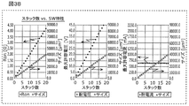
- FIG. 3B is a graph showing the relationship between the number of stacks of switches according to Embodiment 1 and switch characteristics.
- FIG. 4 is an equivalent circuit diagram when the switch of the parallel arm circuit is nonconductive.
- FIG. 5 is a graph showing impedance characteristics, current characteristics, and voltage characteristics of the parallel arm circuit.
- FIG. 6A is a circuit configuration diagram of a parallel arm circuit.
- FIG. 6B is an equivalent circuit diagram of the parallel arm circuit when the switch is nonconductive.
- FIG. 6C is an equivalent circuit diagram at a resonant frequency of the parallel arm circuit when the switch is nonconductive.
- FIG. 6D is an equivalent circuit diagram at a resonant frequency of the parallel arm circuit when the switch is nonconductive.
- FIG. 6E is a circuit configuration diagram of a parallel arm circuit.
- FIG. 6F is an equivalent circuit diagram at a resonant frequency of the parallel arm circuit when the switch is nonconductive.
- FIG. 7 is a graph showing various characteristics of the filter according to Comparative Example 1.
- FIG. 8 is a graph showing various characteristics of the filter according to Comparative Example 2.
- FIG. 9 is a graph showing various characteristics of the filter according to the first embodiment.
- FIG. 10 is a graph showing various characteristics of the filter according to the second embodiment.
- FIG. 11 is a circuit diagram of a filter according to a first modification of the first embodiment.
- FIG. 12 is a graph showing various characteristics of the filter according to the first modification of the first embodiment.
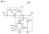
- FIG. 13 is a circuit configuration diagram of a filter according to a second modification of the first embodiment.
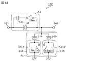
- FIG. 14 is a circuit configuration diagram of a filter according to a third modification of the first embodiment.
- FIG. 15 is a graph showing various characteristics of the filter according to Comparative Example 3.
- FIG. 16 is a graph showing various characteristics of the filter according to the third embodiment.
- FIG. 17 is a circuit configuration diagram of a filter according to a fourth modification of the first embodiment.
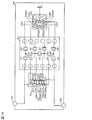
- FIG. 18 is a plan view illustrating the structure of the filter according to the fourth modification of the first embodiment.
- FIG. 19 is a block diagram of the communication apparatus according to the second embodiment.
- the resonant frequency in the resonator or circuit is a resonant frequency for forming an attenuation pole in the pass band or near the pass band of the resonator or the filter including the circuit, and the resonator Alternatively, it is the frequency of the “resonance point” which is a singular point at which the impedance of the circuit becomes minimum (ideally, the point at which the impedance is 0).
- the antiresonance frequency in the resonator or the circuit is an antiresonance frequency for forming an attenuation pole in the pass band or near the pass band of the resonator or the filter including the circuit, unless otherwise specified. It is the frequency of the "anti-resonance point" which is a singular point at which the impedance of the resonator or the circuit concerned is maximal (ideally, the point at which the impedance is infinite).
- the series arm circuit and the parallel arm circuit are defined as follows.
- the parallel arm circuit is a circuit disposed between one node on a path connecting the first input / output terminal and the second input / output terminal and the ground.
- a circuit disposed between the first input / output terminal or the second input / output terminal and a node on the above path to which the parallel arm circuit is connected, or one parallel arm circuit is connected.
- the circuit is disposed between one node on the path and another node on the path to which another parallel arm circuit is connected.
- passband lower end means “the lowest frequency in the passband”.
- pass band high end means “the highest frequency in the pass band”.
- low pass band side means “outside of pass band and lower frequency side than pass band”.
- high pass side of pass band means “outside of pass band and higher frequency side than pass band”.
- the “low frequency side” may be referred to as the “low frequency side”
- the “high frequency side” may be referred to as the “high frequency side”.
- FIG. 1A is a circuit block diagram of filter 10 according to the first embodiment.
- the filter 10 shown in the figure includes a serial arm circuit S1, a parallel arm circuit P1, and an input / output terminal 101 and an input / output terminal 102.
- the filter 10 passes a high frequency signal of a desired frequency among high frequency signals inputted to one of the input / output terminals of the input / output terminals 101 and 102 and outputs the high frequency signal from the other input / output terminals of the input / output terminals 101 and 102. It is a high frequency filter.
- the one input / output terminal is a terminal to which high frequency power is applied.
- the filter 10 When the filter 10 is used as, for example, a transmission filter of a multiplexer or a TDD (Time Division Duplex) filter, high frequency transmission power is applied to one input / output terminal, and high frequency reception power is applied to the other input / output terminal. Applied. However, in this case, of the input / output terminals 101 and 102 to which high frequency power can be applied, a terminal to which higher frequency power is applied is defined as a terminal to which high frequency power of the filter 10 is applied.
- TDD Time Division Duplex
- the series arm circuit S1 is provided on a path connecting the input / output terminal 101 and the input / output terminal 102.
- the series arm circuit S1 includes a series arm resonator s1, a capacitor Cs1 which is an example of a first impedance element, and a switch SWs1 which is a first switch element connected in series with the capacitor Cs1.
- the series arm resonator s1 is connected in parallel with the capacitor Cs1 and the switch SWs1. That is, the circuit in which the capacitor Cs1 and the switch SWs1 are connected in series is connected in parallel to the series arm resonator s1.
- the series arm circuit S1 may have an inductor, which is another example of the first impedance element, instead of the capacitor Cs1.
- Parallel arm circuit P1 is connected to a node on a path connecting input / output terminal 101 and input / output terminal 102, and to ground, and in the present embodiment, between serial arm circuit S1 and input / output terminal 102 Are connected to the node on the above path and to the ground.
- the parallel arm circuit P1 has a parallel arm resonator p1 which is a first parallel arm resonator, and a switch circuit Z1 which is a first switch circuit connected in series to the parallel arm resonator p1.
- the switch circuit Z1 has a switch SWp1 which is a second switch element.
- the parallel arm circuit P1 may be connected to a node on the path between the input / output terminal 101 and the serial arm circuit S1 and to the ground.
- Each of the series arm resonator s1 and the parallel arm resonator p1 is an elastic wave resonator using an elastic wave, and for example, a resonator using a surface acoustic wave (SAW), a bulk acoustic wave (BAW) is used. It is a resonator or a film bulk acoustic resonator (FBAR).
- SAW surface acoustic wave
- BAW bulk acoustic wave
- FBAR film bulk acoustic resonator
- each of the series arm resonator s1 and the parallel arm resonator p1 is configured by an LC element that is an equivalent circuit of a resonator (a circuit in which an inductor and a capacitor are connected in series and a circuit in which a capacitor is connected in parallel) Like a circuit, it may be a resonator or a circuit having a resonance frequency at which the impedance is minimized (ideally 0) and an antiresonance frequency at which the impedance is maximized (ideally infinite).
- the frequency at which the impedance is minimized is referred to as a "resonance frequency” and the frequency at which the impedance is maximized is referred to as an "antiresonance frequency”.
- the capacitor Cs1 is formed, for example, on the same chip as the resonator.
- the capacitor Cs1 may be a variable capacitor such as a varicap and a DTC (Digitally Tunable Capacitor).
- Each of the switches SWs1 and SWp1 is a single pole single throw (SPST) type switch element composed of one or more transistors.
- each of the switches SWs1 and SWp1 is configured of a plurality of transistors.
- each of the switches SWs1 and SWp1 is formed of an FET (Field Effect Transistor), and is formed of, for example, GaAs or a Complementary Metal Oxide Semiconductor (CMOS). Since the switch using such a semiconductor is compact, the filter 10 can be miniaturized. In addition, since the FET has a planar structure and less interference with other elements, it can be easily integrated. Therefore, the filter 10 can be miniaturized and the insertion loss in the pass band can be reduced.
- FET Field Effect Transistor
- the switches SWs1 and SWp1 are switched between conduction and non-conduction respectively according to control signals from a control unit (not shown) such as a radio frequency integrated circuit (RFIC).
- a control unit such as a radio frequency integrated circuit (RFIC).
- RFIC radio frequency integrated circuit
- the resonance frequency of the series arm circuit S1 and the antiresonance frequency of the parallel arm circuit P1 form the passband of the filter 10, and the antiresonance frequency of the series arm circuit S1 and the parallel arm circuit P1.
- the resonant frequency of X forms the attenuation pole of the filter 10.
- the series arm circuit S1 a circuit in which the capacitor Cs1 and the switch SWs1 are connected in series is connected in parallel to the series arm resonator s1. Therefore, by switching the conduction and non-conduction of the switch SWs1, the anti-resonance frequency of the series arm circuit S1 is switched, so that the frequency of the attenuation pole of the filter 10 is switched. Specifically, when the switch SWs1 is nonconductive, the circuit in which the capacitor Cs1 and the switch SWs1 are connected in series does not function, so the anti-resonance frequency of the series arm circuit S1 is approximately equal to the anti-resonance frequency of the series arm resonator s1.
- the capacitor Cs1 is connected in parallel to the series arm resonator s1 by the switch SWs1, so the antiresonance frequency of the series arm circuit S1 is the antiresonance frequency of the series arm resonator s1. Lower than.
- the filter 10 has a frequency variable function of changing the frequency of the attenuation pole according to the switching between the conduction and non-conduction of the switch SWs1.
- the frequency variable width of the attenuation pole depends on the element value of the capacitor Cs1. For example, the larger the element value of the capacitor Cs1, the wider the frequency variable width. Therefore, the element value of the capacitor Cs1 can be appropriately determined in accordance with the frequency specification required for the filter 10.
- the filter 10 has a frequency variable function in which the frequency and the like of the attenuation pole can be switched also by switching on and off of the switch SWp1 of the parallel arm circuit P1. This will be described together with a specific circuit configuration example of the filter 10.
- FIG. 1B is a circuit configuration diagram of filter 10X according to the first embodiment.
- the filter 10X shown in the same drawing is an example of a specific circuit configuration of the filter 10.
- the switch circuit Z1 is one of the switch SWp1 (second switch element) described above, one of an inductor and a capacitor, and a second impedance connected to the switch SWp1. And a capacitor Cp1 which is an example of the element.
- the switch circuit Z1 is a circuit in which a capacitor Cp1 and a switch SWp1 are connected in parallel. Therefore, by switching between conduction and non-conduction of the switch SWp1, the impedance of the switch circuit Z1 is switched. As a result, since the resonant frequency of the parallel arm circuit P1 is switched, the frequency of the attenuation pole of the filter 10X is switched. Specifically, when the switch SWp1 is nonconductive, the capacitor Cp1 is connected in series to the parallel arm resonator p1, so the resonant frequency of the parallel arm circuit P1 is higher than the resonant frequency of the parallel arm resonator p1. . On the other hand, when the switch SWp1 is conductive, the capacitor Cp1 is short-circuited by the switch SWp1, so the resonance frequency of the parallel arm circuit P1 substantially matches the resonance frequency of the parallel arm resonator p1.
- the filter 10X has a frequency variable function of changing the frequency of the attenuation pole according to the switching between the conduction and non-conduction of the switch SWp1.
- the frequency variable width of the attenuation pole depends on the element value of the capacitor Cp1. For example, the smaller the element value of the capacitor Cp1, the wider the frequency variable width. Therefore, the element value of the capacitor Cp1 can be appropriately determined in accordance with the frequency specification required for the filter 10X.
- the filter 10X may have an inductor, which is another example of the second impedance element, instead of the capacitor Cp1.
- the filter 10 which concerns on this Embodiment does not need to be a structure which a switch circuit has a 2nd impedance element like the filter 10X.
- FIG. 1C is another circuit configuration diagram of the filter 10 according to the first embodiment.
- the filter 10Y shown in the same drawing is another example of a specific circuit configuration of the filter 10.
- the parallel arm circuit P1y is another example of the parallel arm circuit P1 included in the filter 10X, and includes a switch circuit Z1y that is another example of the switch circuit Z1 included in the filter 10X.
- the switch circuit Z1y is different from the switch circuit Z1 of the filter 10X in that the capacitor C1 is not included.
- the switch SWp1 is switched between conduction and non-conduction, whereby the impedance of the switch circuit Z1y is switched.
- the pass characteristic of the filter 10Y is a characteristic to which only the series arm circuit S1 contributes (for example, a trap characteristic formed by the series arm circuit S1).
- the pass characteristic of the filter 10Y is the characteristic of a ladder type filter configured of the series arm circuit S1 and the parallel arm resonator p1. That is, the filter 10Y has a frequency variable function of changing the frequency of the pass band and the attenuation band according to the switching between the conduction and non-conduction of the switch SWp1.
- FIG. 2A is a schematic view showing the configuration of the switch IC 50 according to the first embodiment.
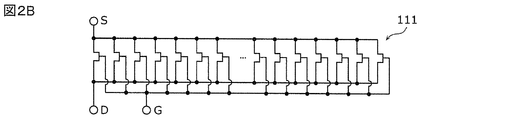
- FIG. 2B is a circuit configuration diagram of the transistor 111 that constitutes the switch IC 50.
- FIG. 2A an implementation of a switch IC including four switches SW1 to SW4 is shown.
- the switches SW1 to SW4 are formed on the substrate 51.
- the power supply terminal P VCC, the control terminal P CTRL, the ground terminal P GND, the switch terminals P SW1, P SW2, P SW3 , P SW4, P SW5 and P SW6 are provided.
- the switch SW1 is connected between the switch terminals P SW1 and P SW6
- the switch SW2 is connected between the switch terminals P SW2 and P SW6
- the switch SW3 is connected between the switch terminals P SW3 and P SW5
- the switch SW4 is connected between P SW4 and P SW5 .
- the switch SWs1 included in the filter 10 corresponds to the switch SW1
- the switch SWp1 corresponds to the switch SW3
- the switches SW2 and SW4 are not yet It becomes use.
- the switch IC 50 is not limited to the configuration shown in FIG. 2A, and may have only the switches SW1 and SW3 among the switches SW1 to SW4 shown in FIG. 2A.
- the substrate 51 is operated by the power supply voltage VCC supplied from, for example, a power supply circuit such as a power management IC, and the conduction and non-conduction of the switches SW1 to SW4 are performed according to the control signal input from, for example, RFIC.
- a control circuit CTRL is provided which generates a plurality of switch drive voltages which are individually switched.
- Each of the switches SW1 to SW4 is composed of one or more transistors 111, and here, has a configuration in which a plurality of transistors 111 are connected in series.
- the transistor 111_1 configuring the switch SW1 includes, for example, a source electrode including a plurality of source electrode fingers 111_1s, a drain electrode including a plurality of drain electrode fingers 111_1d, and a plurality of gate electrode fingers. It is an FET constituted by a gate electrode consisting of 111_1g.
- a source electrode including a plurality of source electrode fingers 111_1s
- a drain electrode including a plurality of drain electrode fingers 111_1d
- gate electrode fingers constituted by a gate electrode consisting of 111_1g.
- the transistor 111_3 configuring the switch SW3 includes, for example, a source electrode including a plurality of source electrode fingers 111_3 s, a drain electrode including a plurality of drain electrode fingers 111_3 d, and a plurality of gates It is an FET constituted by a gate electrode consisting of electrode fingers 111_3g.
- a plurality of unit FETs configured with the source electrode finger, the drain electrode finger, and the gate electrode finger facing each other are arranged in parallel (comb-tooth shape) .
- the switch SW1 ⁇ SW4 configured in this manner, referred to overlap length that the electrode fingers constituting one of the transistor 111 and the finger length L F, a material obtained by multiplying the finger length L F and the finger number N F gate Call it width W. Further, the number of transistors 111 forming one switch is called a stack number Ns.
- the gate width W2 of each of the one or more (here, plural) transistors 111_2 that constitute the switch SW3 is the gate width W1 of at least one of the one or more (here plural) transistors 111_1 that constitute the switch SW1. Greater than. That is, the gate width of each of the transistors constituting the switch SWp1 as the second switch element is larger than the gate width of at least one of the transistors constituting the switch SWs1 as the first switch element.
- the switch SW3 is configured of a plurality of transistors 111_3 having the same configuration
- the switch SW1 is configured of a plurality of transistors 111_1 having the same configuration.
- the gate width W2 of each of the plurality of transistors 111_3 configuring the switch SW3 is larger than any gate width W1 of the plurality of transistors 111_1 configuring the switch SW1.
- the gate width of a transistor that constitutes a switch may be simply referred to as “switch gate width”.
- the finger length L F3 of the switch SW3 of the switch SW1 Longer than finger length L F1 .
- the finger length L F3 of the switch SW3 may be equal to the finger length L F1 of the switch SW1.
- the finger number N F3 of the switch SW3 is greater than the finger number N F1 of the switch SW1.
- the gate widths may be in the above relationship, and the finger lengths and the numbers of fingers may be different from each other.
- the number of stacks of the switch SW1 (here, six) and the number of stacks of the switch SW3 (here, nine) are different from each other. That is, the number of stacks of the switch SWs1 which is the first switch element and the number of stacks of the switch SW3 which is the second switch element are different from each other. Specifically, the number of stacks of the switch SW1 is smaller than the number of stacks of the switch SW3. In the following, the number of stacks of transistors constituting a switch may be simply referred to as “the number of stacks of switches”.
- the switches SWs1 and SWp1 are as follows: It is designed. That is, the gate width of the switch SWp1 of the parallel arm circuit P1 is designed to be larger than the gate width of the switch SWs1 of the series arm circuit S1. Further, the number of stacks of the switch SWs1 is designed to be smaller than the number of stacks of the switch SWp1.
- the filter 10 can ensure power durability while reducing and miniaturizing the insertion loss in the pass band. This will be described using the relationship between the gate width W and the switch characteristics and the relationship between the number of stacks Ns and the switch characteristics.
- the relationship between the number of stacks of the switches SWs1 of the series arm circuit S1 and the number of stacks of the switches SWp1 of the parallel arm circuit P1 is not limited to the above relationship, and may be the same number, for example.
- the total size can be reduced while securing the individual voltage resistances satisfying the power resistance required of the filter 10.
- the number of stacks of the switch SWs1 is preferably designed to be smaller than the number of stacks of the switch SWp1.
- FIG. 3A is a graph showing the relationship between the gate width W and the switch characteristic when the number of stacks Ns is fixed, for the switch formed of the transistor 111.
- FIG. 3B is a graph showing the relationship between the number of stacks Ns and the switch characteristics when the gate width W is fixed, for the switch formed of the transistor 111.
- the on resistance is a resistance at the time of conduction of the switch.
- the withstand voltage maximum allowable voltage at the time of non-conduction
- the switch withstand current maximum allowable current at the time of conduction.
- the gate width W the larger the switch is.
- the withstand voltage and the withstand current of the transistor 111 depend on the widths of the source electrode finger 111s and the drain electrode finger 111d and the gap between the electrode fingers. It is restricted by the material.
- the withstand voltage of one transistor 111 is, for example, about 2.5 V, and the withstand current to the gate width is about 318 mA / mm.
- the larger the number Ns of stacks the larger the on resistance Ron and the withstand voltage of the switch.
- the withstand current is constant regardless of the number of stacks Ns.
- the larger the number of stacks Ns the larger the size.
- the switch formed by the transistor 111 has a trade-off relation that the larger the gate width W, the smaller the ON resistance, but the larger the size.
- the switch has a higher withstand voltage as the number of stacks Ns increases, but on the other hand, there is a trade-off relationship that the on-resistance increases and the size increases.
- the ON resistance decreases as the finger length L F decreases and as the finger number N f increases. This is due to the fact that the shorter the finger length L F, the smaller the resistance component in the longitudinal direction of the electrode finger. Therefore, when the gate width W is fixed, the configuration in which the finger length L F is shortened and the number of fingers is increased can reduce the on resistance as compared with the configuration in which the finger length L F is increased and the number of fingers is reduced. The current resistance can be improved.
- the inventor of the present application has obtained the following knowledge about a high frequency filter having a frequency variable function by the switch SWs1 of the serial arm circuit S1 and the switch SWp1 of the parallel arm circuit P1.
- the switch SWp1 is required to have high current resistance, but the current resistance required for the switch SWs1 is not high. Therefore, by making the gate width of the switch SWp1 larger than the gate width of the switch SWs1, the filter 10 can be miniaturized while securing current resistance. Furthermore, since the on resistance of the switch SWs1 can be reduced, loss can be reduced when the switch SWs1 is conductive.
- the switch SWp1 is required to have high withstand voltage, while the withstand voltage required for the switch SWs1 is not high. Therefore, by making the number of stacks of the switch SWs1 smaller than the number of stacks of the switch SWp1, the filter 10 can be miniaturized while securing the withstand voltage. Further, the switch SWs1 has a smaller gate width than the switch SWp1, and therefore the on resistance per transistor 111 is large, but the number of stacks is small.
- the magnitude of the voltage across the switch SWp1 is proportional to the magnitude of the high frequency power applied to the filter 10.
- the impedance of the switch SWp1 is high, so the voltage across the both ends is large.
- the number of stacks of a plurality of transistors is increased to divide the voltage applied to each transistor.
- the size is increased and the on-resistance of the switch element is increased.
- the size of the switch element is increased, so that the size of the filter is increased, and the withstand voltage of the switch element is improved, whereby the power durability of the filter is improved.
- the on-resistance of the switch element is increased, so that the insertion loss in the pass band of the filter at the time of conduction of the switch element is deteriorated. That is, adjusting the number of stacks of transistors constituting the switch element has a trade-off relationship between the power resistance of the filter, the size of the filter, and the insertion loss in the pass band.
- the magnitude of the voltage across the switch SWp1 across the switch SWp1 is larger when high frequency power is applied to the input / output terminal 101 than when high frequency power is applied to the input / output terminal 102.
- the voltage Vp1 across the switch SWp1 becomes larger.
- the magnitude of the voltage across the switch SWp1 is equal to that of the parallel arm resonator p1 and It is determined by the voltage dividing ratio depending on the impedance ratio of the switch circuit Z1.
- the impedance of the parallel arm resonator p1 largely changes depending on the resonance frequency and the antiresonance frequency
- the high frequency voltage applied to the switch circuit Z1 changes according to the impedance characteristic (that is, resonance characteristic) of the parallel arm resonator p1.
- the magnitude of the voltage Vp1 across the switch SWp1 is determined by which of the input / output terminals 101 and 102 the high frequency power is applied (the high frequency power application direction) and the parallel arm resonator p1 (parallel arm circuit P1). It depends on the resonance frequency.
- FIG. 4 is an equivalent circuit diagram when the parallel arm circuit P1 of the filter 10X or the switch SWp1 of the parallel arm circuit P1y of the filter 10Y is nonconductive.
- the parallel arm circuit Px has a configuration in which a resonator reso and a capacitor Cx are connected in series.
- the resonator reso corresponds to the parallel arm resonator p1 in the parallel arm circuit P1 of the filter 10X or the parallel arm resonator p1 in the parallel arm circuit P1y of the filter 10Y.
- the capacitor Cx corresponds to the off capacitance of the switch SWp1 in the parallel arm circuit P1 of the filter 10X and the combined capacitance of the capacitor Cp1 connected in parallel to the switch SWp1, or the off capacitance of the switch SWp1 in the parallel arm circuit P1y of the filter 10Y.
- the off capacitance of the switch is a capacitance component when the switch is nonconductive (off).
- FIG. 5 is a graph showing impedance characteristics, current characteristics, and voltage characteristics of the parallel arm circuit Px. In the figure, not only the above characteristics of the parallel arm circuit Px but also the above characteristics of the resonator reso and the capacitor Cx constituting the parallel arm circuit Px may be shown.
- the resonant frequency of the parallel arm circuit Px is higher than the resonant frequency of the resonator reso. Further, as shown in the middle part of FIG. 5, the current I flowing through the parallel arm circuit Px is maximum at the resonance frequency of the parallel arm circuit Px. This is due to the fact that the impedance of the parallel arm circuit Px is minimized at the resonant frequency of the parallel arm circuit Px. Further, as shown in the lower part of FIG.
- the voltage V 0 applied to the parallel arm circuit Px is minimized at the resonant frequency of the parallel arm circuit Px, but the voltage V C (absolute value) applied to the capacitor Cx And, the voltage V r (absolute value) applied to the resonator reso is a maximum.
- the voltage V C and the current I of the capacitor Cx become maximum.
- the voltage and the current of the off capacitance and the combined capacitance described as corresponding to the capacitor Cx connected in series to the resonator reso can be maximum at the resonance frequency of the parallel arm circuit Px.
- FIG. 6A is a circuit configuration diagram of the parallel arm circuit Py.
- FIG. 6B is an equivalent circuit diagram of the parallel arm circuit Py in the case where the switch is nonconductive.
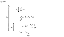
- FIG. 6C is an equivalent circuit diagram at a resonant frequency of the parallel arm circuit Py in the case where the switch is nonconductive.
- the parallel arm circuit Py is a circuit in which a resonator reso and a switch SW are connected in series.
- the resonator reso is represented by a circuit in which a series circuit of an inductor L 1 and capacitors C 1 and R 1 and a capacitance C 0 of the resonator reso are connected in parallel.
- the switch SW is represented by a circuit in which a resistor R off and an off capacitance C off are connected in series.
- “resistance R off ” is a resistance component in the case where the switch SW is nonconductive (off).
- the equivalent circuit at the resonant frequency of the parallel arm circuit Py as shown in FIG. 6C, the inductor L 1 and a resistor R z and capacitor C z is represented by circuits connected in series.
- the resistance R z and the capacitance C z are represented by Expression 1 and Expression 2, respectively.
- the impedance Zp at the resonant frequency of the parallel arm circuit Py is expressed by Equation 3 from the equivalent circuit of FIG. 6C, and the current Ip flowing through the parallel arm circuit Py when the reference voltage Vp is applied to the parallel arm circuit Py is It becomes.
- Equation 5 holds at the resonance frequency of the parallel arm circuit Py.
- the voltage Vc applied to the capacitor Cz becomes Q times the reference voltage Vp of the parallel arm circuit Py, and a voltage exceeding the reference voltage Vp is applied to the switch SW in the parallel arm circuit Py when the switch SW is off. .
- FIG. 6D is an equivalent circuit diagram at a resonant frequency of the parallel arm circuit Py when the switch SW is nonconductive.
- the equivalent circuit shown in FIG. 6D is one in which the capacitor Cz is decomposed into the off capacitance C off of the switch SW.
- the voltage V Coff according to the OFF capacitance C off is represented by the formula 11, as the OFF capacitance C off of the switch SW is small, the voltage across the off capacitance C off of the switch SW is low. Also, as the Q value at the resonance frequency is lower, the voltage applied to the off capacitance C off of the switch SW is lower.
- FIG. 6E is a circuit configuration diagram of the parallel arm circuit Pz.
- FIG. 6F is an equivalent circuit diagram at a resonance frequency of the parallel arm circuit Pz when the switch SW is nonconductive.
- Equation 12 the resonance frequency fr and the anti-resonance frequency fa of the resonator reso are expressed as shown in Equation 12 and Equation 13, respectively.
- Equation 14 the following can be found for the voltage V Coff of the off capacitance C off .
- the capacitance C 0 of the resonator reso increases, the voltage V Coff of the off capacitance C off of the switch SW decreases.
- the capacitor C p1 increases, the voltage V Coff of the off capacitance C off of the switch SW decreases.
- the relative bandwidth (fa ⁇ fr) / fr of the resonator reso increases, the voltage V Coff of the off capacitance C off of the switch SW decreases.
- the magnitude of the voltage Vs across the switch SW is described as being dependent on the high frequency power application direction and the resonant frequency of the parallel arm resonator.
- the magnitude of the voltage Vs across the switch SW is not limited to this, and the capacitance of the parallel arm resonator, the equivalent capacitance C p1 of the switch SW, and the frequency variable width of the parallel arm circuit, Also, it depends on the relative bandwidth of the parallel arm resonator.
- the gate width of the switch SWp1 is larger than the gate width of the switch SWs1, and the number of stacks of the switch SWp1 is larger than the number of stacks of the switch SWs1.
- the filter 10 having a frequency variable function, power resistance can be ensured while achieving reduction and miniaturization of the insertion loss in the pass band.
- Comparative Example 1, Comparative Example 2, Example 1 and Example 2 all have the circuit configuration of the filter 10X, and the same applies except that the high frequency power application direction and the design parameters of the switches SWp1 and SWs1 are different. Is configured.
- Table 1 shows the differences between Comparative Example 1, Comparative Example 2, Example 1 and Example 2. Specifically, in Comparative Example 1 and Example 1, when high frequency power of +36 dBm is applied from the input / output terminal 101, the switch SWs1 is designed to ensure the current resistance and voltage resistance required for the switches SWs1 and SWp1. And SWp1 are designed. Further, in Comparative Example 2 and Example 2, when the high frequency power of +36 dBm is applied from the input / output terminal 102, the switches SWs1 and SWp1 are provided so as to ensure current resistance and voltage resistance required for the switches SWs1 and SWp1. It is designed.
- the switches SWs1 and SWp1 have the same gate width according to the switch requiring the largest current resistance, and the switch requiring the highest voltage resistance is In addition, the number of stacks is set to be the same.
- the gate widths are individually set to ensure the required current resistance, and the number of stacks is set to ensure the required voltage resistance. It is set individually.
- Switch SWs1 is on, switch SWp1 is on: first pass band (700 to 730 MHz) ⁇ Case2> Switch SWs1 is off, switch SWp1 is off: second pass band (710-740 MHz) ⁇ Case3> Switch SWs1 is on, switch SWp1 is off: third pass band (710-730 MHz) ⁇ Case4> Switch SWs1 is off, switch SWp1 is on: fourth pass band (700 to 740 MHz)
- Table 2 shows various design parameters common to the filters according to Comparative Example 1, Comparative Example 2, Example 1 and Example 2. Specifically, in this table, as design parameters, resonance frequency fr, anti-resonance frequency fa and capacitance of series arm resonator s1 and parallel arm resonator p1, and capacitance of capacitor Cs1 and capacitor Cp1 ,It is shown.
- Table 3 shows various characteristics of the filter according to Comparative Example 1, and the maximum current Is_max and the maximum voltage Vs_max applied to each switch. Specifically, in the table, as the various characteristics of the filter, the insertion loss IL, the resonance frequency Fr and the antiresonance frequency Fa of the series arm circuit S1 and the parallel arm circuit P1 are shown for each pass band. The same applies to the same tables thereafter.
- Table 4 shows design parameters, characteristics and sizes of the switches of the filter according to Comparative Example 1. Specifically, in this table, the gate width WF and the number Ns of stacks are shown as design parameters, and the characteristics Ron (on-resistance), allowable input current and allowable input voltage are shown as characteristics. . The same applies to the same tables thereafter.
- FIG. 7 is a graph showing various characteristics of the filter according to Comparative Example 1. Specifically, in the same figure, the pass characteristic of the filter is shown in the first stage from the top (hereinafter referred to as "first stage”). Further, impedance characteristics of the series arm circuits S1 and P1 are shown in the second stage from the top (hereinafter, referred to as “second stage”). In the third from the top (hereinafter, referred to as “third stage”), the characteristics of the current flowing through the switch (switch current characteristics) are shown. In the fourth from the top (hereinafter, referred to as “fourth stage”), the characteristic of the voltage applied to the switch (switch voltage characteristic) is shown.
- first column In the first column from the left (hereinafter, referred to as “first column”), the above-described characteristics in the case where the switch SWs1 is on and the switch SWp1 is on (Case 1) are shown.
- second column In the second column from the left (hereinafter referred to as the “second column”), the above-described characteristics in the case where the switch SWs1 is off and the switch SWp1 is off (Case 2) are shown.
- third column In the third column from the left (hereinafter, referred to as “third column”), the above-described characteristics in the case where the switch SWs1 is on and the switch SWp1 is off (Case 3) are shown.
- fourth column In the fourth column from the left (hereinafter, referred to as “fourth column”), the above-described characteristics in the case where the switch SWs1 is off and the switch SWp1 is on (Case 4) are shown. About these, it is the same also about the graph which shows the various characteristics regarding a subsequent filter.
- Table 5 shows various characteristics of the filter according to Comparative Example 2, and the maximum current Is_max and the maximum voltage Vs_max applied to each switch.
- Table 6 shows design parameters, characteristics and sizes of the switches of the filter according to Comparative Example 2.
- FIG. 8 is a graph showing various characteristics of the filter according to Comparative Example 2.
- Table 7 shows various characteristics of the filter according to the first embodiment, and the maximum current Is_max flowing through each switch and the maximum voltage Vs_max applied.
- Table 8 shows design parameters, characteristics and sizes of the switches of the filter according to the first embodiment.
- FIG. 9 is a graph showing various characteristics of the filter according to the first embodiment.
- Table 9 shows various characteristics of the filter according to the second embodiment, and the maximum current Is_max and the maximum voltage Vs_max applied to each switch.
- Table 10 shows design parameters, characteristics and sizes of the switches of the filter according to the second embodiment.
- FIG. 10 is a graph showing various characteristics of the filter according to the second embodiment.
- Table 11 shows the insertion loss in each pass band and the total size of the two switches for the filters according to Comparative Examples 1 and 2 and Examples 1 and 2.
- Example 1 when Comparative Example 1 and Example 1 are compared, in Example 1, the loss in the passband is reduced, and the total size of the switches can be reduced. Similarly, even when Comparative Example 2 and Example 2 are compared, in Example 2, the loss in the pass band can be reduced, and the total size of the switches can be reduced.
- the impedance of the switch SWs1 is very low (ideally zero), and the first row third stage and the third row third stage in FIGS. As shown in FIG. 5, the current flowing through the switch SWs1 is maximized at the antiresonance frequency of the series arm circuit S1.
- the impedance of the switch SWs1 is very high (ideally infinite), as shown in the second row fourth stage and the fourth row fourth stage in FIGS. 7 to 10, The voltage applied to the switch SWs1 is maximum at the antiresonance frequency of the series arm circuit S1.
- the impedance of the switch SWp1 is very low (ideally zero), and is shown in the first row third stage and the third row third stage in FIGS.
- the current flowing through the switch SWp1 is maximized.
- the switch SWp1 is off, the impedance of the switch SWp1 is very high (ideally infinite), as shown in the second row fourth stage and the fourth row fourth stage in FIGS. 7 to 10, The voltage applied to the switch SWp1 is maximized at the resonant frequency of the parallel arm circuit P1.
- the maximum value of the current of the switch SWp1 is larger than the maximum value of the current of the switch SWs1. Further, when comparing the voltage applied to the switch, the maximum value of the voltage of the switch SWp1 is larger than the maximum value of the voltage of the switch SWs1.
- the switch SWs1 has a gate width smaller than that of the switch SWp1, the required current resistance can be secured.
- the required voltage resistance can be secured.
- the switch element when the gate width is reduced, the on-resistance which is a resistance component at the time of conduction is increased.
- the number of stacks can be reduced, so that the on resistance can be suppressed and the size can be reduced.
- the voltage applied to the switch SWs1 of the series arm circuit S1 is smaller than the voltage applied to the switch SWp1 of the parallel arm circuit P1, and the current flowing to the switch SWs1 of the series arm circuit S1 flows to the switch SWp1 of the parallel arm circuit P1.
- the filters according to the first and second embodiments each have a reduced number of stacks of switches SWs1 of the series arm circuit S1 and a smaller gate width than the filters according to the first and second comparative examples, respectively.
- Example 1 in which high frequency power is applied from the input / output terminal 101 on the side of the series arm circuit S1, high frequency power is received from the input / output terminal 102 on the node side to which the series arm circuit S1 and the parallel arm circuit P1 are connected.
- Example 2 in Example 1, compared with Example 2, the voltage concerning switch SWp1 can be suppressed.
- the voltage applied to the parallel arm circuit P1 is smaller than in the second embodiment in which the high frequency power of the same power is applied from the input / output terminal 102.
- the voltage applied to the switch SWp1 also decreases. Therefore, in this case, in the first embodiment, compared with the second embodiment, even if the number of stacks of the switches SWp1 is reduced, it is possible to secure the required voltage resistance. Therefore, according to the filter of the first embodiment, the size and the on-resistance of the switch SWp1 can be reduced as compared with the second embodiment, so that the size is further reduced and the loss is further reduced when the switch SWp1 is conductive. Is taken.
- the current flowing when the switch SWp1 is on is larger than the current flowing when the switch SWs1 is on. Therefore, the total gate width of the switch SWs1 and the switch SWp1 is reduced while the gate width of each of the one or more transistors constituting the switch SWp1 is larger than the gate width of at least one of the one or more transistors constituting the switch SWs1. It is possible to secure the current resistance that meets the power resistance required for the high frequency filter. Further, since the gate width of the switch SWp1 is relatively large, it is possible to reduce the resistance (on-resistance) when the switch SWp1 conducts. Therefore, the insertion loss in the pass band of the high frequency filter can be reduced when the switch SWp1 conducts.
- the gate width of the switch SWs1 is relatively small, the size of the switch SWs1 can be reduced, so that the filter 10 can be miniaturized. That is, with regard to the high frequency filter having the frequency variable function, power resistance can be secured while achieving reduction and miniaturization of the insertion loss in the pass band.
- the maximum voltage applied to the switch SWs1 is smaller than the maximum voltage applied to the switch SWp1. Therefore, by reducing the number of stacks, the switch SWs1 can be miniaturized while securing the voltage resistance that meets the power resistance required for the high frequency filter. Further, with regard to the switch SWs1, the resistance during conduction can be suppressed by reducing the number of stacks. Therefore, the insertion loss in the pass band of the high frequency filter can be reduced when the switch SWs1 conducts. That is, with regard to the high frequency filter having the frequency variable function, power resistance can be secured while achieving reduction and miniaturization of the insertion loss in the pass band.
- the number of stacks of the switch SWs1 is smaller than the number of stacks of the switch SWp1.
- the number of stacks of the switch SWs1 may be different from the number of stacks of the switch SWp1.
- the number of stacks of the switch SWs1 may be larger than the number of stacks of the switch SWp1.
- the number of stacks of the switch SWs1 (first switch element) and the switch SWp1 (second switch element) is appropriately designed according to the voltage applied during non-conduction.
- the total size can be reduced while securing the individual voltage resistance.
- the resistance during conduction of the one switch can be reduced.
- insertion loss in the passband can be reduced, that is, for a filter having a frequency variable function, power resistance can be ensured while achieving reduction and miniaturization of insertion loss in the passband. .
- parallel arm circuit P1 is not limited to the configuration described in the present embodiment. Therefore, as a modified example of the first embodiment, a filter having a different configuration of the first embodiment and the parallel arm circuit P1 will be described below.
- the switch circuit Z1 in the switch circuit Z1 (first switch circuit), the capacitor Cp1 (second impedance element which is one of the inductor and the capacitor) and the switch SWp1 (second switch element) It was a circuit connected in parallel.
- the switch circuit Z1 further includes an inductor (a third impedance element which is the other of the inductor and the capacitor) connected in series to the switch SWp1. Further, a circuit in which the inductor and the switch SWp1 are connected in series is connected in parallel to the capacitor Cp1.
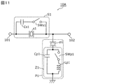
- FIG. 11 is a circuit configuration diagram of a filter 10A according to the first modification of the first embodiment.
- the filter 10A shown in the figure differs from the filter 10X described above in the configuration of the switch circuit Z1.
- the description of the same points as the filter 10X will be omitted, and differences will be mainly described.
- the filter 10A includes series arm circuits S1 and S5, a parallel arm circuit P1, and input / output terminals 101 and 102.
- the switch circuit Z1 has a capacitor Cp1 (second impedance element), a switch SWp1 (second switch element), and an inductor Lp1 (third impedance element).
- the inductor Lp1 is connected in series to the switch SWp1, and a circuit in which the inductor Lp1 and the switch SWp1 are connected in series is connected in parallel to the capacitor Cp1.
- the switch SWp1 switches from conduction to non-conduction, whereby the resonance frequency of the parallel arm circuit P1 is switched to the high frequency side.
- the resonance frequency of the parallel arm circuit can be positioned lower than the resonance frequency of the parallel arm resonator p1 by the inductor Lp1 connected in series to the switch SWp1. For this reason, by switching the conduction and non-conduction of the switch SWp1, the variable width of the frequency of the attenuation pole on the lower side of the pass band can be increased compared to the filter 10X described above.
- design parameters of respective elements other than the inductor Lp1 are as shown in Table 2. Further, with respect to the switches SWs1 and SWp1, the magnitude relation between gate widths and the magnitude relation between the numbers of stacks are the same as in the first embodiment.
- FIG. 12 is a graph showing various characteristics of the filter 10A according to the first modification of the first embodiment. Specifically, various characteristics in the case where there is no inductor Lp1 (when the inductor Lp1 is short-circuited) in the same figure and when the element value of the inductor Lp1 is 2.0 nH, 4.0 nH and 8.0 nH It is shown.
- the first stage is a graph showing the impedance characteristics of the series arm circuit S1 and the parallel arm circuit P1
- the second stage is a graph showing an enlarged part of the frequency range of the impedance characteristic shown in the first stage. is there.
- the third stage is a graph showing filter characteristics.
- the switch circuit Z1 is a circuit in which the capacitor Cp1 and the inductor Lp1 are connected in parallel. Therefore, in this case, the parallel arm circuit P1 is a circuit in which the parallel arm resonator p1 and a circuit in which the capacitor Cp1 and the inductor Lp1 are connected in parallel are connected in series. Furthermore, since the frequency at which the impedance of the circuit in which the capacitor Cp1 and the inductor Lp1 are connected in parallel is maximized is set higher than the resonance frequency of the parallel arm resonator p1, a switch is used at the resonance frequency of the parallel arm resonator p1.
- the circuit Z1 has an inductive impedance.
- the resonance frequency of the parallel arm circuit P1 is located lower than the resonance frequency of the parallel arm resonator p1. Specifically, as shown in the second and third stages of FIG. 12, as the element value of the inductor Lp1 is larger, the resonance frequency of the parallel arm circuit P1 is located on the lower frequency side.
- the parallel arm circuit P1 is equivalent to a circuit in which the parallel arm resonator p1 and the capacitor Cp1 are connected in series. Therefore, the resonant frequency of the parallel arm circuit P1 is switched to the higher frequency side than the resonant frequency of the parallel arm resonator p1.
- filter 10A according to the first modification of the first embodiment increases the variable width of the frequency of the attenuation pole in the lower region of the pass band by inductor Lp1 connected in series with switch SWp1. be able to. Therefore, the filter 10A according to the first modification of the first embodiment can ensure a large variable width of the pass band.
- the switch circuit Z1 (first switch circuit) is not limited to the above configuration, and may have a plurality of circuits in which an inductor Lp1 (third impedance element) and a switch SWp1 (second switch element) are connected in series. I do not mind. At this time, the plurality of sets of circuits are connected in parallel to each other and in parallel to the capacitor Cp1 (second impedance element). According to such a configuration, it is possible to finely switch the frequency of the attenuation pole on the low pass band side by appropriately switching conduction and non-conduction of the switches SWp1 of each set.
- the inductance values of the plurality of inductors Lp1 may be different from each other, or the inductance values of two or more inductors Lp1 of the plurality of inductors Lp1 may be equal.
- the Q value of the combined inductor is improved, and since there are a plurality of switches SWp1 in parallel, the Q value of the resonant frequency of the parallel arm circuit P1 can be increased, High selectivity of the filter 10A is possible.
- one parallel arm circuit includes one parallel arm resonator
- one parallel arm circuit may include two parallel arm resonators. Therefore, the filter according to the second modification of the first embodiment configured as described above will be described below.
- FIG. 13 is a circuit configuration diagram of a filter 10B according to the second modification of the first embodiment.
- the filter 10B shown in the figure differs from the filter 10X described above in the configuration of the switch circuit Z1.
- the description of the same points as the filter 10X will be omitted, and differences will be mainly described.
- the parallel arm circuit P1 includes parallel arm resonators p1a and p1b, and a switch circuit Z1a connected in series to the parallel arm resonator p1a.
- the resonance frequency of the parallel arm resonator p1b is different from the resonance frequency of the parallel arm resonator p1a
- the antiresonance frequency of the parallel arm resonator p1b is different from the antiresonance frequency of the parallel arm resonator p1a.
- the parallel arm resonator p1a, the capacitor Cp1a, the switch SWp1a and the switch circuit Z1a respectively correspond to the parallel arm resonator p1, the capacitor Cp1, the switch SWp1 and the switch circuit Z1 in the filter 10X.
- the parallel arm circuit P1 of the filter 10B further includes a parallel arm resonator p1a (first parallel arm resonator) and a switch circuit Z1a (first switch circuit) in series, as compared to the parallel arm circuit P1 of the filter 10X. It has a parallel arm resonator p1 b (second parallel arm resonator) connected in parallel to the connected circuit.
- the switch SWp1a switches from conduction to non-conduction, whereby the pass characteristic of the filter 10B has an attenuation slope on the low pass band side. It will switch to the high frequency side while maintaining the steepness.
- the filter can switch the frequency of the low pass end of the pass band and the frequency of the attenuation band to the high side while suppressing an increase in insertion loss at the low pass end of the pass band. That is, it is possible to switch the frequency of the attenuation pole on the low pass side of the pass band without deteriorating the insertion loss in the pass band.
- the switch SWp1a switches from conduction to non-conduction, whereby the pass characteristic of the filter 10B is attenuated by the high pass band in the pass band.
- the slope is switched to the high frequency side while maintaining the steepness.
- the filter can switch the frequency of the high pass end of the pass band and the frequency of the attenuation band to the high pass while suppressing the increase of the insertion loss of the high pass end of the pass band. That is, it is possible to switch the frequency of the attenuation pole on the high band side of the pass band without deteriorating the insertion loss in the pass band.
- the capacitance of the parallel arm resonator p1a connected in series with the switch circuit Z1a is greater than the capacitance of the parallel arm resonator p1b. It is preferable to be large.
- the switch SWp1a (second switch element) is included in the switch circuit Z1a (first switch circuit) connected in series with the parallel arm resonator p1a. Therefore, when the switch SWp1a is not conducting, the voltage applied to the off-capacitance component of the switch SWp1a depends on the capacitance of the parallel arm resonator p1a, and more specifically, the parallel arm resonator p1a The larger the capacitance of the capacitor, the smaller (see [4. Analysis of voltage applied to switches in parallel arm circuit]).
- the voltage applied to the switch SWp1a can be lowered by making the capacitance of the parallel arm resonator p1a larger than the capacitance of the parallel arm resonator p1b, so the number of stacks of the switches SWp1a can be reduced. Is possible. Therefore, the switch SWp1a can be miniaturized while securing the voltage resistance.
- FIG. 14 is a circuit configuration diagram of a filter 10C according to the third modification of the first embodiment.
- the filter 10C shown in the same figure has two sets of circuits in which the parallel arm circuit P1 has a series connection of parallel arm resonators and a switch circuit, and these two sets of circuits are connected in parallel It differs in that it is done.
- the description of the same points as the filter 10B will be omitted, and differences will be mainly described.
- the parallel arm circuit 21 includes parallel arm resonators p1a and p1b, a switch circuit Z1a connected in series to the parallel arm resonator p1a, and a switch circuit Z1b connected in series to the parallel arm resonator p1b. .
- the circuit in which the parallel arm resonator p1a and the switch circuit Z1a are connected in series and the circuit in which the parallel arm resonator p1b and the switch circuit Z1b are connected in series are connected in parallel.
- the switch circuit Z1b is a circuit including a capacitor Cp1b and a switch SWp1b. The switch SWp1 b is connected in parallel to the capacitor Cp1 b.
- the switch circuit Z1b may have an inductor instead of the capacitor Cp1.
- the resonance frequency of the parallel arm resonator p1b is different from the resonance frequency of the parallel arm resonator p1a, and the antiresonance frequency of the parallel arm resonator p1b is different from the antiresonance frequency of the parallel arm resonator p1a.
- the resonance frequency of the parallel arm resonator p1b is lower than the resonance frequency of the parallel arm resonator p1a
- the antiresonance frequency of the parallel arm resonator p1b is lower than the antiresonance frequency of the parallel arm resonator p1a.
- the switch SWp1a is switched from conduction to non-conduction
- the switch SWp1b is switched from conduction to non-conduction, whereby the pass characteristic of the filter 10C is on the low pass side of the pass band.
- the passband can be switched to the high band side while maintaining the steepness of the attenuating slope of the above and the steepness of the attenuation slope on the high band side of the pass band.
- the passband can be switched to the high band side while suppressing an increase in insertion loss at the low band end of the pass band.
- the passband lower band side attenuation pole is switched to the lower band side, and the passband high band side attenuation pole is switched to the low band side
- the passband The passband can be switched to the low band side while suppressing an increase in the insertion loss at the high band end. That is, it is possible to switch the frequency of the attenuation pole on the low pass band side and the high pass band side of the pass band without deteriorating the insertion loss in the pass band.
- the switch SWp1b is configured of one or more transistors, as in the switches SWs1 and SWp1a.
- the switches SWs1, SWp1a and SWp1b that perform the frequency variable function of the filter 10C in this way are designed as follows.
- each of the switches SWs1, SWp1a and SWp1b will be described as being configured of one or more transistors having the same configuration.
- Gate width of switch SWs1 ⁇ gate width of switch SWp1a Gate width of switch SWs1 ⁇ gate width of switch SWp1b Number of stacks of switch SWp1b> Number of stacks of switch SWs1> Number of stacks of switch SWp1a
- Comparative Example 3 and Example 3 both have the circuit configuration of the filter 10C, and are configured similarly except that the design parameters of the switches SWp1a, SWp1b, and SWs1 are different.
- Comparative Example 3 and Example 3 when the high frequency power of +36 dBm is applied from the input / output terminal 102, the current resistance and voltage resistance required for the switches SWs1, SWp1a and SWp1b are ensured.
- the switches SWs1, SWp1a and SWp1b are designed.
- the switches SWs1, SWp1a, and SWp1b have the same gate width according to the switch requiring the largest current resistance, and match the switch requiring the highest voltage resistance.
- the number of stacks is set to be the same.
- the switches SWs1, SWp1a, and SWp1b have their gate widths individually set to ensure the required current resistance, and the number of stacks individually set to ensure the required voltage resistance. It is set.
- the parallel arm resonator p1a connected in series with the switch circuit Z1a (first switch circuit) is described as a first parallel arm resonator, and the switch circuit is connected in series with the switch circuit.
- the parallel arm resonator p1b not connected is described as the second parallel arm resonator.
- the parallel arm resonator having high resonance frequency and antiresonance frequency (here, the parallel arm resonator p1b) is the first parallel It becomes an arm resonator, and a parallel arm resonator with low resonance frequency and antiresonance frequency (here, parallel arm resonator p1a) becomes a second parallel arm resonator.
- the switch circuit (here, the switch circuit Z1b) connected in series to the parallel arm resonator having high resonance frequency and antiresonance frequency is the first switch circuit.
- a switch circuit (here, switch circuit Z1a) connected in series to a parallel arm resonator having a low resonant frequency and an antiresonant frequency is a second switch circuit. That is, the switch element (here, switch SWp1 b) and the impedance element (here, capacitor Cp1 b) which the switch circuit connected in series to the parallel arm resonator having high resonance frequency and antiresonance frequency respectively have the second switch element and the second switch element. 3 becomes an impedance element.
- switch element here, switch SWp1a
- impedance element here, capacitor Cp1a
- the frequency of the passband is switched as follows by switching conduction (on) and non-conduction (off) of the switches SWs1, SWp1a and SWp1b.
- High frequency filter tunable filter
- ⁇ Case1> The switch SWs1 is on, the switch SWp1a is on, and the switch SWp1b is on: first pass band (705-725 MHz) ⁇ Case2>
- the switch SWs1 is off, the switch SWp1a is off, and the switch SWp1b is off: second pass band (710 to 735 MHz) ⁇ Case3>
- the switch SWs1 is on, the switch SWp1a is off, and the switch SWp1b is on: third pass band (710-725 MHz) ⁇ Case4>
- the switch SWs1 is off, the switch SWp1a is on, the switch SWp1b is off: fourth pass band (705-735 MHz)
- Table 12 shows various design parameters common to the filters according to Comparative Example 3 and Example 3. Specifically, in this table, as design parameters, resonance frequency fr, antiresonance frequency fa and capacitance of series arm resonator s1 and parallel arm resonators p1a and p1b, and capacitors Cs1 and Cp1a and Cp1b Capacitance is shown.
- Table 13 shows various characteristics of the filter according to Comparative Example 3, and the maximum current Is_max and the maximum voltage Vs_max applied to each switch. Specifically, in this table, as the various characteristics of the filter, the insertion loss IL, the resonant frequency Fr1 and the antiresonant frequency Fa1 of the series arm circuit S1, and the two resonant frequencies Fr1 and Fr1 of the parallel arm circuit P1 for each passband. Fr2 and antiresonance frequencies Fa1 and Fa2 are shown. The same applies to the same tables thereafter.
- Table 14 shows design parameters, characteristics and sizes of the switches of the filter according to Comparative Example 3.
- FIG. 15 is a graph showing various characteristics of the filter according to Comparative Example 3. Specifically, in the figure, the pass characteristic of the filter is shown in the first stage. The second stage shows the impedance characteristics of the series arm circuits S1 and P1. In the third stage, the characteristics of the current flowing through the switch (switch current characteristics) are shown. Also, the fourth stage shows the characteristics of the voltage applied to the switch (switch voltage characteristics). Further, in the same column, the first column shows the above characteristics in the case where the switch SWs1 is on, the switch SWp1a is on, and the switch SW1b is on (Case 1).
- the second column shows the above-mentioned characteristics in the case where the switch SWs1 is off, the switch SWp1a is off, and the switch SWp1b is off (Case 2).
- the third column shows the above-mentioned characteristics in the case where the switch SWs1 is on, the switch SWp1a is off, and the switch SWp1b is off (Case 3).
- the fourth column the above characteristics in the case where the switch SWs1 is off, the switch SWp1a is on, and the switch SWp1b is off (Case 4) are shown. About these, it is the same also about the graph which shows the various characteristics regarding a subsequent filter.
- Table 15 shows various characteristics of the filter according to the third embodiment, and the maximum current Is_max and the maximum voltage Vs_max applied to each switch.
- Table 16 shows design parameters, characteristics and sizes of the switches of the filter according to the third embodiment.
- FIG. 16 is a graph showing various characteristics of the filter according to the third embodiment.
- Table 17 shows the insertion loss in each passband and the total size of the three switches for the filters according to Comparative Example 3 and Example 3.
- the impedance of the switch SWs1 is very low (ideally zero), and the first row third stage and the third row third stage of FIGS. As shown in FIG. 5, the current flowing through the switch SWs1 is maximized at the antiresonance frequency of the series arm circuit S1.
- the switch SWs1 is off, the impedance of the switch SWs1 is very high (ideally infinite), as shown in the second row fourth stage and the fourth row fourth stage in FIGS.
- the voltage applied to the switch SWs1 is maximum at the antiresonance frequency of the series arm circuit S1.
- the impedance of the switch SWp1a is very low (ideally zero), and is shown in the first row third stage and the fourth row third stage in FIGS.
- the current flowing through the switch SWp1a is maximized at the resonance frequency on the low frequency side of the parallel arm circuit P1 (ie, the resonance frequency of the parallel arm resonator p1a).
- the switch SWp1a is off, the impedance of the switch SWp1a is very high (ideally infinite), as shown in the second row fourth stage and the third row fourth stage in FIGS.
- the voltage applied to the switch SWp1a is maximum at the resonance frequency on the low frequency side of the parallel arm circuit P1.
- the impedance of the switch SWp1b is very low (ideally zero), and the first row third stage and the third row third stage of FIGS.
- the current flowing through the switch SWp1b is maximum at the resonance frequency on the high frequency side of the parallel arm circuit P1 (ie, the resonance frequency of the parallel arm resonator p1b).
- the switch SWp1b is off, the impedance of the switch SWp1b is very high (ideally infinite), as shown in the second row fourth stage and the fourth row fourth stage in FIGS.
- the voltage applied to the switch SWp1b is maximized at the resonance frequency on the high frequency side of the parallel arm circuit P1.
- the maximum value of the current of the switch SWs1 is smaller than both the maximum value of the current of the switch SWp1a and the maximum value of the current of the switch SWp1b. Further, comparing the voltage applied to the switch, the maximum value of the voltage of the switch SWp1a is smaller than the maximum value of the voltage of the switch SWs1, and the maximum value of the voltage of the switch SWp1b is larger than the maximum value of the voltage of the switch SWs1.
- the switch SWs1 has a smaller gate width than the switches SWp1a and SWp1b, it is possible to secure necessary current resistance. Further, the switch SWp1a can ensure necessary voltage resistance even when the number of stacks is reduced as compared with the switch SWs1.
- the gate width of the switch SWs1 (first switch element) is the switch SWp1a (third switch element) and the switch SWp1b (second Smaller than any gate width of the switch element).
- the switch SWs1, the switch SWp1a, and the switch SWp1b it is possible to secure current resistance that satisfies the power resistance required for the filter 10C while reducing the total size.
- the gate widths of the switches SWp1a and SWp1b are relatively large, it is possible to reduce the resistance (on-resistance) when the switches SWp1a and SWp1b are conductive.
- the insertion loss in the pass band of the filter 10C can be reduced.
- the filter 10C that can switch the frequency of the attenuation pole without deteriorating the insertion loss at the pass band end it is possible to ensure the power resistance while reducing the insertion loss in the pass band and reducing the size.
- the maximum voltage applied to switch SWs1 is smaller than the maximum voltage applied to switch SWp1b, and the maximum voltage applied to switch SWp1a is applied to switch SWs1. Less than the maximum voltage. Therefore, the number of stacks of the switch SWs1 is smaller than the number of stacks of the switch SWp1b, and the number of stacks of the switch SWp1a is smaller than the number of stacks of the switch SWs1. As a result, the total size of the switch SWs1 and the switch SWp1a can be reduced while securing the respective withstand voltage characteristics satisfying the power resistance required of the filter 10C.
- the resistance during conduction can be suppressed by reducing the number of stacks. Therefore, when the switch SWs1 and the switch SWp1a conduct, the insertion loss in the pass band of the filter 10C can be reduced. That is, in the filter 10C in which the frequency of the attenuation pole can be switched without deteriorating the insertion loss at the pass band end, the power resistance can be ensured while achieving further reduction and further miniaturization of the insertion loss in the pass band. .
- the switch SWs1, the switch SWp1a, and the switch SWp1b satisfy the relationship of the number of stacks
- the present invention is not limited to this.
- the number of stacks of the switch SWs1, the number of stacks of the switch SWp1a, and the number of stacks of the switch SWp1b may be the same.
- the following effects can be obtained by the switch SWs1, the switch SWp1a, and the switch SWp1b satisfying the above-described gate width relationship. That is, for the switch SWs1, the switch SWp1a, and the switch SWp1b, it is possible to reduce the total size while securing the individual voltage resistances that satisfy the power resistance required of the filter 10C. As a result, in the filter 10C, power resistance can be ensured while achieving reduction and downsizing of the insertion loss in the pass band.
- FIG. 17 is a circuit configuration diagram of a filter 10D according to the fourth modification of the first embodiment.
- the filter 10D includes series arm circuits S1, S2, S3, S4, and S5, parallel arm circuits P1, P2, P3, and P4, and input / output terminals 101 and 102.
- the series arm circuit S1 is a series arm circuit provided on a path connecting the input / output terminal 101 and the input / output terminal 102.
- the series arm circuit S2 is a series arm circuit provided closer to the input / output terminal 102 than the series arm circuit S1 in the path shape.
- the series arm circuit S3 is a series arm circuit provided closer to the input / output terminal 102 than the series arm circuit S2 in the path shape.
- the series arm circuit S4 is a series arm circuit provided closer to the input / output terminal 102 than the path-like series arm circuit S3.
- the series arm circuit S5 is a series arm circuit provided closer to the input / output terminal 102 than the path-like series arm circuit S4.
- the series arm circuit S1 includes a series arm resonator s1, a capacitor Cs1, and a switch SWs1.
- the switch SWs1 is a switch element connected in series to the capacitor Cs1 and configured by one or more transistors.
- a circuit in which the capacitor Cs1 and the switch SWs1 are connected in series is connected in parallel to the series arm resonator s1.
- the series arm circuit S2 includes a series arm resonator s2, a capacitor Cs2, and a switch SWs2.
- the switch SWs2 is a switch element connected in series to the capacitor Cs2 and configured by one or more transistors.
- a circuit in which the capacitor Cs2 and the switch SWs2 are connected in series is connected in parallel to the series arm resonator s2.
- the series arm circuit S3 includes a series arm resonator s3, a capacitor Cs3, and a switch SWs3.
- the switch SWs3 is a switch element connected in series to the capacitor Cs3 and configured by one or more transistors.
- a circuit in which the capacitor Cs3 and the switch SWs3 are connected in series is connected in parallel to the series arm resonator s3.
- the series arm circuit S4 includes a series arm resonator s4, a capacitor Cs4, and a switch SWs4.
- the switch SWs4 is a switch element connected in series to the capacitor Cs4 and configured by one or more transistors.
- a circuit in which the capacitor Cs4 and the switch SWs4 are connected in series is connected in parallel to the series arm resonator s4.
- the series arm circuit S5 includes a series arm resonator s5, a capacitor Cs5, and a switch SWs5.
- the switch SWs5 is a switch element connected in series to the capacitor Cs5 and configured by one or more transistors.
- a circuit in which the capacitor Cs5 and the switch SWs5 are connected in series is connected in parallel to the series arm resonator s5.
- the parallel arm circuit P1 is connected to a node on the path between the series arm circuits S1 and S2 and to the ground.
- the parallel arm circuit P2 is connected to the node on the path between the series arm circuits S2 and S3 and to the ground.
- the parallel arm circuit P3 is connected to the node on the path between the series arm circuits S3 and S4 and to the ground.
- the parallel arm circuit P4 is connected to the node on the path between the series arm circuits S4 and S5 and to the ground.
- the parallel arm circuit P1 has a parallel arm resonator p1 and a switch circuit Z1 connected in series to the parallel arm resonator p1.
- the parallel arm circuit P2 has a parallel arm resonator p2 and a switch circuit Z2 connected in series to the parallel arm resonator p2.
- the parallel arm circuit P3 has a parallel arm resonator p3 and a switch circuit Z3 connected in series to the parallel arm resonator p3.
- the parallel arm circuit P4 has a parallel arm resonator p4 and a switch circuit Z4 connected in series to the parallel arm resonator p4.
- the switch circuit Z1 has a capacitor Cp1 and a switch SWp1.
- the switch SWp1 is connected in parallel to the capacitor Cp1 and is configured of one or more transistors.
- the switch circuit Z2 has a capacitor Cp2 and a switch SWp2.
- the switch SWp2 is connected in parallel to the capacitor Cp2 and is configured of one or more transistors.
- the switch circuit Z3 has a capacitor Cp3 and a switch SWp3.
- the switch SWp3 is connected in parallel to the capacitor Cp3 and includes one or more transistors.
- the switch circuit Z4 has a capacitor Cp4 and a switch SWp4.
- the switch SWp4 is connected in parallel to the capacitor Cp4 and is configured of one or more transistors.
- a passband is formed by the resonance frequency of the series arm circuits S1 to S5 and the antiresonance frequency of the parallel arm circuits P1 to P5.
- the antiresonance frequency of the series arm circuits S1 to S5 constitutes an attenuation pole on the high side of the pass band
- the resonance frequency of the parallel arm circuits P1 to P5 constitutes an attenuation pole on the low side of the pass band.
- the conduction and non-conduction of the switches SWs1 to SWs5 are respectively switched, whereby the antiresonance frequencies of the series arm circuits S1 to S5 are respectively switched.
- filter 10D can finely adjust the frequency of the passband and the frequency of the attenuation band by appropriately switching conduction and non-conduction of switches SWs1 to SWs5 and SWp1 to SWp4.
- the gate widths and the number of stacks of the switches SWs1 to SWs5 and SWp1 to SWp4 are set individually.
- each of the switches SWs1 to SWs5 and SWp1 to SWp4 is described as being configured of one or more transistors having the same configuration.
- the gate width of at least one of the switches SWp1 to SWp4 is designed to be larger than the gate width of at least one of the switches SWs1 to SWs5. That is, the gate widths of the switches SWs1 to SWs5 and SWp1 to SWp4 are individually set so as to ensure the required current resistance. Further, the number of stacks of at least one of the switches SWp1 to SWp4 is designed to be different from the number of stacks of at least one of the switches SWs1 to SWs5.
- the number of stacks of the switches SWs1 to SWs5 and SWp1 to SWp4 may be the same.
- FIG. 18 is a plan view for explaining the structure of the filter 10D shown in FIG.
- the series arm resonators s1 to s5 and the parallel arm resonators p1 to p4 are surface acoustic wave resonators having IDT (InterDigital Transducer) electrodes formed on the substrate 41 having piezoelectricity, or formed on the substrate 41.
- Bulk acoustic wave resonator which is configured in one package.
- the switches SWs1 to SWs5 and the capacitors Cs1 to Cs5 are configured in a package 43 different from the series arm resonators s1 to s5 and the parallel arm resonators p1 to p4.
- the switches SWp1 to SWp4 and the capacitors Cp1 to Cp4 are formed in a package 42 different from the series arm resonators s1 to s5 and the parallel arm resonators p1 to p4. These three packages are mounted on the wiring substrate 44 and connected by the wiring formed on the wiring substrate 44.
- the capacitors Cs1 to Cs5 and the capacitors Cp1 to Cp4 are formed in the package on the switch side.
- the respective resonators are configured It may be configured on the substrate 41.
- the switch circuit configured by the capacitor and the switch is disposed on the ground side among the node side and the ground side on the path connecting the input / output terminals 101 and 102.
- the switch circuit when the switch circuit is disposed on the node side, the number of terminals needs to be increased in both the package including the resonator and the package including the switch, and the size becomes large. From this viewpoint, by arranging the switch circuit on the ground side of the node side and the ground side with respect to the parallel arm resonator, it is possible to miniaturize the filter 10D.
- the filters described in the first embodiment and its examples can also be applied to multiplexers and high frequency front end circuits that support systems with a higher number of bands. Therefore, in the second embodiment, such a multiplexer, a high frequency front end circuit, and a communication apparatus will be described.
- FIG. 19 is a block diagram of the communication device 5 according to the second embodiment.
- the communication apparatus 5 includes a switch group 310 formed of a plurality of switches, a filter group 320 formed of a plurality of filters, transmission side switches 331 and 332, and reception side switches 351 and 352, and 353, transmission amplification circuits 341 and 342, reception amplification circuits 361 and 362, an RF signal processing circuit (RFIC) 3, a baseband signal processing circuit (BBIC) 4, and an antenna element 2.
- RFIC RF signal processing circuit
- BBIC baseband signal processing circuit
- the switch group 310 connects the antenna element 2 and a signal path corresponding to a predetermined band in accordance with a control signal from a control unit (not shown), and is formed of, for example, a plurality of SPST type switches.
- the number of signal paths connected to the antenna element 2 is not limited to one, and may be plural. That is, the communication device 5 may support carrier aggregation.
- the filter group 320 is configured by, for example, a plurality of filters (including duplexers) having the next band in the pass band.
- the band is (i) transmission band of Band12, (ii) transmission band of Band13, (iii) transmission band of Band14, (iv) transmission band of Band27, (v) transmission band of Band26, vi) Band29 and Band14 or Band12, Band67 and Band13 reception band, (vii-Tx) Band68 or Band28a or Band28b transmission band, (vii-Rx) Band68 or Band28a or Band28b reception band, (viii-Tx) Band20 A transmission band, a reception band of (viii-Rx) Band 20, a transmission band of (ix-Tx) Band 27 or Band 26, a transmission band of (x-Tx) Band 8 and a reception band of (x-Rx) Band 8
- the transmission side switch 331 is a switch circuit having a plurality of selection terminals connected to a plurality of transmission side signal paths on the low band side with low center frequency among the bands in the filter group 320 and a common terminal connected to the transmission amplification circuit 341 It is.
- the transmission side switch 332 is a switch having a plurality of selection terminals connected to a plurality of transmission side signal paths on the high band side having a high center frequency among bands in the filter group 320 and a common terminal connected to the transmission amplification circuit 342 It is a circuit.
- the transmission side switches 331 and 332 are switch circuits which are provided in the front stage of the filter group 320 (here, the front stage in the transmission side signal path) and switch the connection state according to the control signal from the control unit (not shown). .
- the high frequency signals here, high frequency transmission signals
- the transmission amplification circuits 341 and 342 are output to the antenna element 2 through the predetermined filters of the filter group 320.
- the reception side switch 351 is a switch circuit having a plurality of selection terminals connected to a plurality of reception side signal paths on the low band side having a low center frequency among the bands in the filter group 320 and a common terminal connected to the reception amplification circuit 361 It is.
- the receiving switch 352 has a common terminal connected to the receiving signal path of a predetermined band (here, Band 20), and two selection terminals connected to the common terminal of the receiving switch 351 and the common terminal of the receiving switch 352.
- the reception-side switch 353 is a switch having a plurality of selection terminals connected to a plurality of reception-side signal paths on the high band side with high center frequency among the bands in the filter group 320 and a common terminal connected to the reception amplification circuit 362 It is a circuit.
- the reception side switches 351 to 353 are provided at the subsequent stage of the filter group 320 (here, the subsequent stage in the reception side signal path), and the connection state is switched according to the control signal from the control unit (not shown).
- the high frequency signal (here, high frequency received signal) input to the antenna element 2 is amplified by the reception amplifier circuits 361 and 362 through the predetermined filters of the filter group 320, and the RF signal processing circuit (RFIC) Output to
- the RF signal processing circuit (RFIC) corresponding to the low band and the RF signal processing circuit (RFIC) corresponding to the high band may be provided separately.
- the transmission amplifier circuit 341 is a power amplifier that amplifies the power of a low band high frequency transmission signal
- the transmission amplifier circuit 342 is a power amplifier that amplifies the power of a high band high frequency transmission signal.
- the reception amplifier circuit 361 is a low noise amplifier that power-amplifies a low band high frequency reception signal
- the reception amplification circuit 362 is a low noise amplifier that powers a high band high frequency reception signal.
- the RF signal processing circuit (RFIC) 3 is a circuit that processes a high frequency signal transmitted and received by the antenna element 2. Specifically, the RF signal processing circuit (RFIC) 3 performs signal processing of a high frequency signal (here, a high frequency received signal) input from the antenna element 2 via the receiving signal path by down conversion or the like, and the signal The received signal generated by processing is output to the baseband signal processing circuit (BBIC) 4. Further, the RF signal processing circuit (RFIC) 3 performs signal processing on the transmission signal input from the baseband signal processing circuit (BBIC) 4 by up conversion and the like, and generates a high frequency signal (high frequency in this case) generated by the signal processing. The transmission signal is output to the transmission side signal path.
- a high frequency signal here, a high frequency received signal
- BBIC baseband signal processing circuit
- the communication device 5 configured in this way is (vi) a filter having the reception band of Band 29 and Band 14 or Band 12 or Band 67, Band 67 and Band 13 in the pass band, (vii-Tx) Band 68 or Band 28 a or Band 28 b transmission band as the pass band As at least one of the filters having the (vii-Rx) Band 68 or Band 28 a or Band 28 b reception band in the pass band, the (ix-Tx) Band 27 or Band 26 transmission band in the pass band, Embodiment 1 And a filter according to any of the embodiments. That is, the filter switches the frequency of the passband and the frequency of the attenuation band according to the control signal.
- the control unit constitutes the high frequency front end circuit 1.
- the switch group 310 and the filter group 320 constitute a multiplexer.
- the filter group 320 may be connected to the common terminal through the switch group 310 as in the second embodiment, and a plurality of filters according to the first embodiment may be It may be configured to be directly connected to the common terminal.
- control unit may be included in an RF signal processing circuit (RFIC), or may constitute a switch IC together with each switch controlled by the control unit. Good.
- RFIC RF signal processing circuit
- the high frequency front end circuit 1 and the communication device 5 configured as described above, by providing the filters according to the first embodiment and the example thereof, the required power resistance can be secured and the size can be reduced. And, high-performance high-frequency front end circuit 1 and communication device 5 can be realized which can reduce the insertion loss in the pass band at the time of conduction of each switch. That is, according to the high frequency front end circuit 1, it is possible to secure power durability while improving the gain in the pass band and reducing the size. Further, according to the communication device 5, it is possible to secure the power durability while improving the communication quality and reducing the size.
- the size can be reduced.
- the transmission side switches 331 and 332 and the reception side switches 351 to 353 switch circuits provided at the front or rear of the filter group 320 (a plurality of high frequency filters) ).
- the transmission amplification circuits 341 and 242 or the reception amplification circuits 361 and 362 (amplification circuits) corresponding to a plurality of high frequency filters can be shared. Therefore, miniaturization and cost reduction of the high frequency front end circuit can be realized.
- the transmission switches 331 and 332 and the reception switches 351 to 353 may be provided.
- the number of transmission side switches 331 and 332 and the number of reception side switches 351 to 353 are not limited to the number described above, and, for example, one transmission side switch and one reception side switch are provided. I don't care.
- the number of selection terminals and the like of the transmission side switch and the reception side switch is not limited to that of the second embodiment, and may be two.
- the number of series arm circuits may be two or more, or five or more.
- each of the series arm resonator and the parallel arm resonator described above is not limited to one resonator, and may be configured by a plurality of divided resonators in which one resonator is divided.
- each switch element is composed of a plurality of transistors (specifically, FET) having the same configuration, for the sake of simplicity.
- FET field-effect transistor
- the configuration of each switch element is not limited to the above, and the configuration of at least one transistor may be different from the configuration of other transistors. That is, in each switch element, the gate widths of the plurality of transistors are not limited to the same but may be different.
- the current resistance of the switch element configured by connecting a plurality of transistors in series is limited by the current resistance of the transistor having the smallest gate width among the plurality of transistors (that is, the restriction is imposed) Will be Therefore, in order to satisfy the current resistance required for the switch element formed of a plurality of transistors, it is necessary to satisfy the current resistance for each of the plurality of transistors.
- the gate width of each of the plurality of transistors that constitute the second switch element is a plurality of elements that constitute the first switch element.
- the gate width of at least one of the transistors of As a result, with respect to the second switch element and the first switch element, it is possible to secure current resistance that satisfies the power resistance required for a high frequency filter or the like while reducing the total size.
- a switch element configured by connecting a plurality of transistors in series, even if the gate widths of other transistors different from the transistor with the smallest gate width are increased, the current resistance of the entire switch element is improved. Not only that, it hinders miniaturization. Therefore, in order to miniaturize the switch element, it is necessary not to make the gate width too large for the other transistors.
- the gate widths of the plurality of transistors constituting the first switch element are It may be smaller than any gate width of the transistor.
- the first switch element can be further miniaturized while securing current resistance that satisfies the power resistance required for a high frequency filter or the like. That is, the high-frequency filter or the like including the first switch element can be further miniaturized while reducing the insertion loss in the passband and ensuring the power durability.
- each switch element was comprised by several transistors.
- control unit may be provided outside the RF signal processing circuit (RFIC) 3, and may be provided, for example, in the high frequency front end circuit 1.
- the high frequency front end circuit 1 is not limited to the above-described configuration, and may include a high frequency filter having a frequency variable circuit, and a control unit for controlling conduction and non-conduction of switch elements of the frequency variable circuit. Absent. According to the high frequency front end circuit 1 configured as described above, it is possible to switch the passband according to the required frequency specification while suppressing an increase in the insertion loss at the passband end.
- an inductor or a capacitor may be connected between each component.
- the inductor may include a wiring inductor formed by wiring connecting the components.
- the present invention is widely applicable to communication devices such as mobile phones as small filters, multiplexers, front end circuits and communication devices applicable to multi-band systems.
- RFIC radio frequency identification circuit
- BBIC Base band signal processing circuit
Landscapes
- Physics & Mathematics (AREA)
- Acoustics & Sound (AREA)
- Chemical & Material Sciences (AREA)
- Crystallography & Structural Chemistry (AREA)
- Engineering & Computer Science (AREA)
- Computer Networks & Wireless Communication (AREA)
- Signal Processing (AREA)
- Filters And Equalizers (AREA)
Abstract
La présente invention concerne un filtre (10) pourvu d'un circuit à bras série (S1) et d'un circuit à bras parallèles (P1). Le circuit à bras série (S1) comprend un condensateur (Cs1), un commutateur (SWs1) connecté en série avec le condensateur (Cs1), et un résonateur à bras série (s1) connecté en parallèle au condensateur (Cs1) et au commutateur (SWs1). Le circuit à bras parallèles (P1) est pourvu d'un résonateur à bras parallèles (p1) et d'un circuit de commutation (Z1) connecté en série au résonateur à bras parallèles (p1). Le circuit de commutation (Z1) comprend un commutateur (SWp1). Chacun des commutateurs (SWs1 et SWp1) est formé à partir d'un ou de plusieurs transistors. La largeur de grille de chacun du ou des transistors constituant le commutateur (SWp1) est supérieure à la largeur de grille d'au moins un transistor parmi l'un ou les transistors constituant le commutateur (SWs1).
Priority Applications (1)
| Application Number | Priority Date | Filing Date | Title |
|---|---|---|---|
| US16/733,239 US11489514B2 (en) | 2017-07-10 | 2020-01-03 | Radio-frequency filter, multiplexer, radio-frequency front-end circuit, and communication device |
Applications Claiming Priority (2)
| Application Number | Priority Date | Filing Date | Title |
|---|---|---|---|
| JP2017-134989 | 2017-07-10 | ||
| JP2017134989 | 2017-07-10 |
Related Child Applications (1)
| Application Number | Title | Priority Date | Filing Date |
|---|---|---|---|
| US16/733,239 Continuation US11489514B2 (en) | 2017-07-10 | 2020-01-03 | Radio-frequency filter, multiplexer, radio-frequency front-end circuit, and communication device |
Publications (1)
| Publication Number | Publication Date |
|---|---|
| WO2019013015A1 true WO2019013015A1 (fr) | 2019-01-17 |
Family
ID=65001578
Family Applications (1)
| Application Number | Title | Priority Date | Filing Date |
|---|---|---|---|
| PCT/JP2018/024735 Ceased WO2019013015A1 (fr) | 2017-07-10 | 2018-06-28 | Filtre haute fréquence, multiplexeur, circuit frontal haute fréquence et dispositif de communication |
Country Status (2)
| Country | Link |
|---|---|
| US (1) | US11489514B2 (fr) |
| WO (1) | WO2019013015A1 (fr) |
Families Citing this family (4)
| Publication number | Priority date | Publication date | Assignee | Title |
|---|---|---|---|---|
| WO2019073899A1 (fr) * | 2017-10-10 | 2019-04-18 | 株式会社村田製作所 | Multiplexeur et filtre haute fréquence |
| CN115004550A (zh) * | 2020-01-24 | 2022-09-02 | 株式会社村田制作所 | 滤波器装置、多工器、高频前端电路以及通信装置 |
| CN117792420A (zh) * | 2022-09-20 | 2024-03-29 | 深圳市中兴微电子技术有限公司 | 收发机射频开关及其开关电路、控制方法以及存储介质 |
| CN117240265A (zh) * | 2023-08-25 | 2023-12-15 | 锐磐微电子科技(上海)有限公司 | 射频开关电路、芯片以及射频前端模组 |
Citations (6)
| Publication number | Priority date | Publication date | Assignee | Title |
|---|---|---|---|---|
| JPH098621A (ja) * | 1995-06-16 | 1997-01-10 | Nec Corp | Fetスイッチ回路 |
| JP2000323961A (ja) * | 1999-03-10 | 2000-11-24 | Matsushita Electric Ind Co Ltd | 弾性表面波共振器を用いた帯域切替フィルタとそれを用いたアンテナ共用器 |
| JP2008011320A (ja) * | 2006-06-30 | 2008-01-17 | Sony Corp | 半導体スイッチ回路並びに通信機器 |
| JP2009130831A (ja) * | 2007-11-27 | 2009-06-11 | Samsung Electronics Co Ltd | チューナブルフィルタ |
| JP2014502803A (ja) * | 2010-12-10 | 2014-02-03 | ペレグリン セミコンダクター コーポレイション | 共振器回路及び共振器の調整のための方法、システム、及び装置 |
| WO2016208677A1 (fr) * | 2015-06-24 | 2016-12-29 | 株式会社村田製作所 | Filtre à ondes élastiques, multiplexeur, duplexeur circuit frontal à haute fréquence, et dispositif de communication |
Family Cites Families (3)
| Publication number | Priority date | Publication date | Assignee | Title |
|---|---|---|---|---|
| JPH10336000A (ja) | 1997-06-05 | 1998-12-18 | Nec Eng Ltd | 高周波信号切り替え器 |
| FR2927742A1 (fr) | 2008-02-15 | 2009-08-21 | St Microelectronics Sa | Filtre a resonateur acoustiques de type baw reconfigurable par voie numerique et procede |
| US8838045B2 (en) * | 2009-12-03 | 2014-09-16 | Rf Micro Devices, Inc. | Sub-band duplexer with active frequency tuning |
-
2018
- 2018-06-28 WO PCT/JP2018/024735 patent/WO2019013015A1/fr not_active Ceased
-
2020
- 2020-01-03 US US16/733,239 patent/US11489514B2/en active Active
Patent Citations (6)
| Publication number | Priority date | Publication date | Assignee | Title |
|---|---|---|---|---|
| JPH098621A (ja) * | 1995-06-16 | 1997-01-10 | Nec Corp | Fetスイッチ回路 |
| JP2000323961A (ja) * | 1999-03-10 | 2000-11-24 | Matsushita Electric Ind Co Ltd | 弾性表面波共振器を用いた帯域切替フィルタとそれを用いたアンテナ共用器 |
| JP2008011320A (ja) * | 2006-06-30 | 2008-01-17 | Sony Corp | 半導体スイッチ回路並びに通信機器 |
| JP2009130831A (ja) * | 2007-11-27 | 2009-06-11 | Samsung Electronics Co Ltd | チューナブルフィルタ |
| JP2014502803A (ja) * | 2010-12-10 | 2014-02-03 | ペレグリン セミコンダクター コーポレイション | 共振器回路及び共振器の調整のための方法、システム、及び装置 |
| WO2016208677A1 (fr) * | 2015-06-24 | 2016-12-29 | 株式会社村田製作所 | Filtre à ondes élastiques, multiplexeur, duplexeur circuit frontal à haute fréquence, et dispositif de communication |
Also Published As
| Publication number | Publication date |
|---|---|
| US11489514B2 (en) | 2022-11-01 |
| US20200144992A1 (en) | 2020-05-07 |
Similar Documents
| Publication | Publication Date | Title |
|---|---|---|
| US10911027B2 (en) | Radio-frequency filter, multiplexer, radio-frequency front-end circuit, and communication device | |
| US10862456B2 (en) | Acoustic wave filter device, multiplexer, radio frequency front-end circuit, and communication device | |
| US11876506B2 (en) | Acoustic wave filter device | |
| US10812048B2 (en) | Acoustic wave filter device, radio-frequency front-end circuit, and communication apparatus | |
| US10630257B2 (en) | Acoustic wave filter device, multiplexer, radio-frequency front-end circuit, and communication apparatus | |
| US10720903B2 (en) | Acoustic wave filter device, radio-frequency front-end circuit, and communication apparatus | |
| US10958242B2 (en) | Acoustic wave filter device, multiplexer, radio-frequency front end circuit, and communication device | |
| US10944381B2 (en) | Acoustic wave filter device, multiplexer, radio-frequency front end circuit, and communication device | |
| US10715110B2 (en) | Acoustic wave filter device, multiplexer, RF front-end circuit, and communication apparatus | |
| US11139798B2 (en) | Radio-frequency filter, multiplexer, radio-frequency front-end circuit, and communication device | |
| WO2019021983A1 (fr) | Filtre à haute fréquence, multiplexeur, circuit frontal à haute fréquence et dispositif de communication | |
| US10819310B2 (en) | Radio-frequency filter circuit, multiplexer, radio-frequency front-end circuit, and communication apparatus | |
| US11476835B2 (en) | High-frequency filter circuit, high-frequency front end circuit, and communication device | |
| US10742193B2 (en) | Acoustic wave filter device, RF front-end circuit, and communication apparatus | |
| WO2018097203A1 (fr) | Dispositif de filtre à ondes élastiques, multiplexeur, circuit frontal à haute fréquence, et dispositif de communication | |
| US11489514B2 (en) | Radio-frequency filter, multiplexer, radio-frequency front-end circuit, and communication device | |
| US10727810B2 (en) | Radio-frequency filter, multiplexer, radio-frequency front-end circuit, and communication device | |
| WO2018051864A1 (fr) | Circuit frontal haute fréquence et appareil de communication | |
| US10840886B2 (en) | Radio-frequency filter, multiplexer, radio-frequency front-end circuit, and communication device | |
| CN111201709B (zh) | 弹性波滤波器、多工器、高频前端电路以及通信装置 | |
| US11394368B2 (en) | Acoustic wave filter, multiplexer, radio frequency front-end circuit, and communication device | |
| US20200228097A1 (en) | Multiplexer and high-frequency filter |
Legal Events
| Date | Code | Title | Description |
|---|---|---|---|
| 121 | Ep: the epo has been informed by wipo that ep was designated in this application |
Ref document number: 18832033 Country of ref document: EP Kind code of ref document: A1 |
|
| NENP | Non-entry into the national phase |
Ref country code: DE |
|
| 122 | Ep: pct application non-entry in european phase |
Ref document number: 18832033 Country of ref document: EP Kind code of ref document: A1 |
|
| NENP | Non-entry into the national phase |
Ref country code: JP |