WO2019017066A1 - Capteur magnétique ultra-petit à haute sensibilité - Google Patents
Capteur magnétique ultra-petit à haute sensibilité Download PDFInfo
- Publication number
- WO2019017066A1 WO2019017066A1 PCT/JP2018/019705 JP2018019705W WO2019017066A1 WO 2019017066 A1 WO2019017066 A1 WO 2019017066A1 JP 2018019705 W JP2018019705 W JP 2018019705W WO 2019017066 A1 WO2019017066 A1 WO 2019017066A1
- Authority
- WO
- WIPO (PCT)
- Prior art keywords
- magnetic
- coil
- asic
- substrate film
- ultra
- Prior art date
- Legal status (The legal status is an assumption and is not a legal conclusion. Google has not performed a legal analysis and makes no representation as to the accuracy of the status listed.)
- Ceased
Links
Images
Classifications
-
- G—PHYSICS
- G01—MEASURING; TESTING
- G01R—MEASURING ELECTRIC VARIABLES; MEASURING MAGNETIC VARIABLES
- G01R33/00—Arrangements or instruments for measuring magnetic variables
- G01R33/02—Measuring direction or magnitude of magnetic fields or magnetic flux
- G01R33/028—Electrodynamic magnetometers
- G01R33/0283—Electrodynamic magnetometers in which a current or voltage is generated due to relative movement of conductor and magnetic field
-
- G—PHYSICS
- G01—MEASURING; TESTING
- G01R—MEASURING ELECTRIC VARIABLES; MEASURING MAGNETIC VARIABLES
- G01R33/00—Arrangements or instruments for measuring magnetic variables
- G01R33/02—Measuring direction or magnitude of magnetic fields or magnetic flux
- G01R33/06—Measuring direction or magnitude of magnetic fields or magnetic flux using galvano-magnetic devices
-
- H—ELECTRICITY
- H10—SEMICONDUCTOR DEVICES; ELECTRIC SOLID-STATE DEVICES NOT OTHERWISE PROVIDED FOR
- H10B—ELECTRONIC MEMORY DEVICES
- H10B61/00—Magnetic memory devices, e.g. magnetoresistive RAM [MRAM] devices
-
- H—ELECTRICITY
- H10—SEMICONDUCTOR DEVICES; ELECTRIC SOLID-STATE DEVICES NOT OTHERWISE PROVIDED FOR
- H10N—ELECTRIC SOLID-STATE DEVICES NOT OTHERWISE PROVIDED FOR
- H10N50/00—Galvanomagnetic devices
- H10N50/01—Manufacture or treatment
-
- H—ELECTRICITY
- H10—SEMICONDUCTOR DEVICES; ELECTRIC SOLID-STATE DEVICES NOT OTHERWISE PROVIDED FOR
- H10N—ELECTRIC SOLID-STATE DEVICES NOT OTHERWISE PROVIDED FOR
- H10N59/00—Integrated devices, or assemblies of multiple devices, comprising at least one galvanomagnetic or Hall-effect element covered by groups H10N50/00 - H10N52/00
-
- G—PHYSICS
- G01—MEASURING; TESTING
- G01R—MEASURING ELECTRIC VARIABLES; MEASURING MAGNETIC VARIABLES
- G01R33/00—Arrangements or instruments for measuring magnetic variables
- G01R33/02—Measuring direction or magnitude of magnetic fields or magnetic flux
- G01R33/06—Measuring direction or magnitude of magnetic fields or magnetic flux using galvano-magnetic devices
- G01R33/063—Magneto-impedance sensors; Nanocristallin sensors
Definitions
- the present invention relates to a technology for miniaturizing the size and thickness of a GSR sensor by integrally forming a GSR element and an application specific integrated circuit (hereinafter referred to as ASIC).
- the GSR sensor is a high sensitivity micro magnetic sensor based on ultra-fast spin rotation effect (English notation; GHz Spin Rotation effect).
- High sensitivity micro magnetic sensors include horizontal FG sensors, vertical FG sensors, Hall sensors, GMR sensors, TMR sensors, MI sensors, GSR sensors, high frequency carrier sensors, and the like. At present, these sensors are widely adopted in smartphones, automobiles, medical care, robots and the like. Among them, the GSR sensor (Patent Document 1) is excellent in sensitivity surface and size, and is most noted.
- Patent Document 4 In order to miniaturize the GSR sensor, multifaceted efforts have been made such as miniaturizing the GSR element, miniaturizing the ASIC, and joining method of both parts (Patent Document 4). However, in any of the approaches, since the element and the ASIC are separately separated and manufactured as two parts, there is a limit in the point of miniaturization, particularly reduction in thickness, since the two are joined (Patent Documents 4 and 5) ).
- the inventor forms a film to be a substrate of the GSR element on the insulating protective film of the ASIC main body, and forms grooves for arranging magnetic wires on the substrate film. It was conceived that thickness reduction could be achieved by integrally forming a GSR element consisting of a magnetic wire and a detection coil around the magnetic wire.
- oxides such as SiO 2 and Al 2 O 3 and nitrides such as SiN are possible. That is, when these substrate films are used, when forming the GSR element directly on the ASIC surface, the processing of the micro groove included in the manufacturing process of the GSR element, CF 4 gas plasma treatment, resist heat curing There were steps such as processing and development processing using acid and alkali, and damage to the insulating protective film on the ASIC surface and deterioration of the functionality of the ASIC circuit under the GSR element substrate due to the damage were not observed.
- the area of the entire GSR element could be reduced by reducing the size of the electrode by adopting a through-hole type joint which penetrates the substrate film and the insulating protective film for bonding the ASIC and the GSR element.
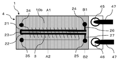
- FIG. 1 is a plan view of a GSR sensor and a GSR element in the embodiment and the example.
- FIG. 2 is a cross-sectional view taken along line A1-A2 of FIG.
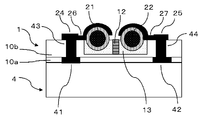
- FIG. 3 is a cross-sectional view taken along line B1-B2 of FIG.
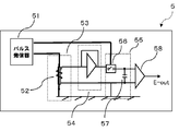
- FIG. 4 is a diagram of the electronic circuit in the embodiment and the example.
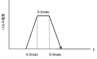
- FIG. 5 is a diagram showing the relationship between the passage of the conduction time and the application of the pulse current when the pulse current is supplied to the element.
- the ultra-compact high-sensitivity magnetic sensor according to the present invention comprises an insulating protective film formed on an ASIC and a wiring plane of the ASIC, a substrate film formed on the protective film, and a magnetic field detection element formed on the substrate film
- the magnetic field detection element is composed of a magnetic wire and a detection coil and electrodes that circulate around the magnetic wire on the substrate film.
- the magnetic wire has a two-phase magnetic domain structure of a surface magnetic domain having conductivity and an anisotropic magnetic field of 20 G or less and having a circumferential spin alignment and a central core magnetic domain having an axial spin alignment.
- the detection coil has a coil pitch of 10 ⁇ m or less.
- the electrode penetrates the substrate film and the insulating protective film, and is directly bonded to the element connection electrode of the ASIC in a through hole manner.
- a film having a thickness capable of serving as a substrate of the magnetic field detection element is formed on the insulating protective film on the surface of the ASIC, and the film is used as the substrate.
- a groove is attached to the substrate film, and a magnetic wire is aligned with the groove to produce a magnetic field detection element. That is, the sensor formed of the magnetic field detection element integrally formed with the ASIC can be thinned, and can be miniaturized.
- the ASIC of the ultra-compact high-sensitivity magnetic sensor of the present invention is generated when a pulse current of a converted frequency of 0.2 GHz to 4.0 GHz is caused to flow through the magnetic wire of the magnetic field detection element and a pulse current flows through the magnetic wire. It comprises means for detecting the coil voltage and means for converting the coil voltage into an electrical signal proportional to the external magnetic field H. Note that high sensitivity can be realized by supplying a pulse current of 0.2 to 4.0 GHz.
- the thickness of the substrate film of the ultra-compact high-sensitivity magnetic sensor of the present invention is 1 ⁇ m to 20 ⁇ m.
- the substrate coating needs to be thick enough to be grooved to receive the magnetic wire.
- the diameter of the magnetic wire assumed is 1 ⁇ m to 10 ⁇ m.
- the thickness of the substrate film is preferably 1 ⁇ m to 20 ⁇ m.
- a sufficient thickness to have a function as a substrate in the insulating protective film is secured, a single-layer structure in which the insulating protective film doubles as the substrate film is also possible.
- the magnetic field detection element has a groove 1 ⁇ m to 10 ⁇ m deep from the top surface of the substrate film, and a part or all of the detection coil is embedded. According to the present invention, the magnetic field detection element can be miniaturized.
- FIG. 1 a plan view of a GSR sensor and a GSR sensor element (hereinafter referred to as an element) is shown in FIG. 1, a sectional view taken along line A1-A2 of the plan view is shown in FIG. 2, and a sectional view taken along line B1-B2. 3 show an embodiment of the present invention in detail.
- the magnetic wire consists of two, and the form which consists of 2 layers of an insulation protective film and a board
- the ultra-compact high-sensitivity magnetic sensor (hereinafter referred to as a sensor) of the present invention comprises a GSR sensor element 1 (hereinafter referred to as an element) and ASIC 4 and electrodes for external wiring (45 and 46) from the ASIC 4.
- the element 1 constituting the sensor includes two magnetic wires 2 (21 and 22) and one coil 3 around the magnetic wires on a substrate film 10b formed on the insulating protective film 10a of the ASIC 4 and Two electrodes (24 and 25) for wire conduction, two electrodes (34 and 35) for coil voltage detection, and connections (26 and 27) between magnetic wire and wire conduction electrode, coil and coil detection Connection part with electrode, through-hole type joint between coil electrode on the element side and coil electrode on ASIC side, through-hole type joint between wire electrode on the element side and wire electrode on ASIC side (43 and 44) It consists of Further, the element 2 includes a wire connecting portion 23 as means for supplying pulse current in the reverse direction to two magnetic wires.
- two coil electrodes and two wire electrodes are connected to the element 1 by the through-hole electrode junctions respectively, and a coil is generated in the detection coil when a pulse current is supplied to the element It comprises an electronic circuit that senses the voltage and converts the coil voltage into an external magnetic field.
- external wiring electrodes 45 and 46 are disposed in the ASIC.
- the external magnetic field H and the coil voltage Vs are represented by a mathematical relationship such as the following equation (1), and are converted into the external magnetic field H using this relationship.
- Vs V 0 ⁇ 2L ⁇ ⁇ D ⁇ p ⁇ Nc ⁇ f ⁇ sin ( ⁇ H / 2Hm) (1)
- Vs coil output voltage
- V 0 proportional constant
- L length of wire
- D diameter of wire
- p skin depth of pulse current
- Nc number of turns of coil
- f pulse frequency
- Hm Is the external magnetic field strength when the coil output voltage takes a maximum value.
- the structure of the device 1 is as shown in FIGS.
- the size of the element 1 is the size of the substrate 10, which is 0.07 mm to 0.4 mm wide and 0.25 mm to 1 mm long.
- the thickness is 10 ⁇ m to 15 ⁇ m. Therefore, since the thickness of the ASIC 4 is 30 ⁇ m to 100 ⁇ m, the thickness of the sensor is 40 ⁇ m to 115 ⁇ m.
- a groove 11 with a width of 20 ⁇ m to 60 ⁇ m and a depth of 1 ⁇ m to 10 ⁇ m is formed in the substrate film 10b so that two magnetic wires (21 and 22) can be aligned in parallel.
- the two magnetic wires (21 and 22) are close, and the distance between the two magnetic wires is 1 ⁇ m to 10 ⁇ m.
- the magnetic wire 21 and the magnetic wire 22 are separated by an insulating material, and for example, separation by the insulating separation wall 12 is preferable.
- the magnetic wire 2 has a diameter of 1 ⁇ m to 10 ⁇ m of a CoFeSiB alloy.
- the periphery of the magnetic wire 2 is preferably coated with an insulating material, for example, an insulating glass material.
- the length is 0.07 mm to 1 mm.
- the anisotropic magnetic field of the magnetic wire 2 is 20 G or less, and has a two-phase magnetic domain structure of a surface magnetic domain having a circumferential spin alignment and a central core magnetic domain having an axial spin alignment.
- the coil 3 has 6 to 180 turns and a coil pitch of 0.2 to 10 ⁇ m.
- the distance between the coil 3 and the magnetic wire 2 is 0.2 ⁇ m to 3 ⁇ m.
- the average coil inner diameter is 2 ⁇ m to 35 ⁇ m.
- a substrate film 10b is formed on the insulating protective film 10a on the surface of the ASIC, a groove with a depth of 1 ⁇ m to 10 ⁇ m is attached to the substrate film 10b, and the element is embedded to embed part to all of the coil along the groove surface.
- the thickness of the element portion 1 can be 20 ⁇ m or less from the surface of the ASIC. Further, by setting the thickness of the ASIC to about 30 ⁇ m, the thickness of the entire sensor can be set to about 50 ⁇ m.
- the substrate film 10 b can be formed on the insulating protective film 10 a on the top surface of the ASIC to form the device 1.
- a two-layered film of an insulating protective film and a substrate film is formed, it is possible to use a single-layered film as long as the insulating protective film has a sufficient thickness to have a function as a substrate.
- a SiO 2 (silicon dioxide) film is formed with a thickness of 0.5 ⁇ m to 2 ⁇ m on an ASIC surface by vacuum evaporation or the like, and a SiN (silicon nitride) film is further formed on the upper surface of the film It is formed with a thickness of ⁇ 10 ⁇ m.
- a groove with a depth of 1 ⁇ m to 10 ⁇ m is attached to the SiN film, and an element is formed so as to embed part or all of the coil along the groove surface.
- Electrode wiring is performed on the lower coil 31 and the substrate film surface along the groove 11 formed in the substrate film 10b. Thereafter, an insulating separation wall 12 is formed at the central portion of the groove 11 to form two groove shapes, and two glass-coated magnetic wires (21 and 22) are respectively aligned and arranged there. Next, an insulating resist is applied to the entire surface of the substrate film. Thus, the magnetic wires (21 and 22) are fixed in the groove 11. The top of the magnetic wires (21 and 22) is thinly applied during this application.
- the upper coil 32 is formed there by photolithography.
- the material of the substrate film is not limited to oxide and nitride as long as the characteristics required here are satisfied.
- an insulating material is apply
- the concave lower coil 31 is formed along the groove surface of the groove 11 formed in the substrate film 10 b and both sides of the groove 11.
- the convex upper coil 32 is electrically connected to the lower coil 31 through the joint portion 33 to form a spiral coil 3.
- the glass of the insulating coating material is removed to allow electrical connection by metal deposition.
- the wire input electrode (+) 24 is connected to the upper magnetic wire 21 and is connected to the lower magnetic wire 22 via the wire connection portion 23.
- the lower magnetic wire 22 is connected to the wire output electrode ( ⁇ ) 25. Due to this wire connection portion, a leftward pulse current flows from the right to the left in the magnetic wire 21 and a rightward pulse (reverse to the magnetic wire 21) from the left to the right in the magnetic wire 22. The current can flow.
- the coil output electrode (+) 34 is connected to the upper end of the coil 3
- the coil ground electrode ( ⁇ ) is connected to the lower end of the coil 3.
- the electrode on the element side and the electrode on the ASIC side are electrically connected via a through hole type joint (43 and 44) penetrating the insulating protective film 10a and the substrate film 10b as shown in the example of FIG. Ru.
- the magnetic wire input electrode (+) 24 on the element side is a wire electrode (+) 41 on the ASIC side through the through-hole type electrode joint portion (+) 43 penetrating the insulating protective film 10a and the substrate film 10b.
- the magnetic wire output electrode (-) 25 on the element side is connected to the wire electrode (-) on the ASIC side via the through-hole type electrode joint (-) 44 that penetrates the insulating protective film 10a and the substrate film 10b. It shows that it is connected to 42.
- the coil electrode on the element side and the coil electrode on the ASIC side are connected via an electrode joint portion penetrating the insulating protective film 10 a and the substrate film 10 b.
- the electronic circuit 5 is shown in FIG. 4 with reference to the pulse corresponding buffer circuit described in Patent Document 1.
- the electronic circuit 5 is connected to an element 52 for outputting a coil voltage, and a pulse oscillation circuit 51 for transmitting a pulse current to the element 52, an input circuit 53 for inputting a coil voltage, a pulse corresponding buffer circuit 54, a coil
- the sample and hold circuit 55 including an electronic switch 56 for detecting the peak voltage of the rising pulse output waveform and the capacitor 57 having a capacitance of 4 pF to 100 pF for holding the peak voltage and amplification by the programming amplifier of the amplifier 58 performs AD conversion. Transfer the signal to an external signal processor with two wires.
- AD conversion is 14 bits to 16 bits.
- the capacitance is preferably 4 pF to 8 pF.
- the conversion frequency of the pulse current is 0.2 GHz to 4 GHz
- the intensity of the pulse current is 50 mA to 200 mA
- the pulse conduction time is 2 nsec or less.
- FIG. 5 shows the relationship between the passage of the conduction time and the application of the pulse current when the pulse current is supplied to the element. In the example of FIG. 5, it rises at 0.5 nsec, holds a predetermined pulse time of 0.5 nsec in its applied state, and falls at 0.5 nsec.
- the coil output is a sine wave output with a measurement range of 3 G to 100 G, and its sensitivity is 50 mV / G to 3 V / G.
- the linearity of the coil output is 0.3% or less.
- FIG. 1 is a plan view of the GSR sensor and the GSR sensor element according to the embodiment
- FIG. 2 is a cross-sectional view taken along line A1-A2 of the plan view
- FIG. 3 is a cross-sectional view taken along line B1-B2.
- the size of the element 1 is 0.10 mm in width and 0.40 mm in length.
- the thickness 40 of the ASIC 4 is 50 ⁇ m
- the thickness 14 of the insulating protective film 10 a and the substrate film 10 b is 8 ⁇ m
- the thickness of the convex portion of the element is 2 ⁇ m
- the thickness of the sensor combining these is 60 ⁇ m.
- a groove 11 having a width of 20 ⁇ m and a depth of 3 ⁇ m is formed in the substrate film 10b so that two magnetic wires (21 and 22) can be aligned in parallel.
- the two magnetic wires (21 and 22) are in close proximity, and the distance between the magnetic wires is 3 ⁇ m, and the magnetic wires (21 and 22) are separated by the insulating separation wall 12 with a thickness of 3 ⁇ m.
- the magnetic wire 2 is 5 ⁇ m in diameter of the CoFeSiB amorphous alloy.
- the periphery of the magnetic wire 2 is covered with an insulating glass.
- the length is 0.40 mm.
- the anisotropic magnetic field of the magnetic wire 2 is 15 G, and has a two-phase magnetic domain structure of a surface magnetic domain having a circumferential spin alignment and a central core magnetic domain having an axial spin alignment.
- the coil 3 has 100 turns and a coil pitch of 3 ⁇ m.
- the distance between the coil 3 and the magnetic wire 2 is 2 ⁇ m, and the average coil inner diameter is 8 ⁇ m
- a substrate film 10b having a thickness of 7 ⁇ m is formed on the insulating protective film 10a on the upper surface of the ASIC, and a groove having a depth of 3 ⁇ m is attached thereto to fabricate an element 1.
- the capacitance of the capacitor 57 of the electronic circuit 5 is 6 pF.
- the conversion frequency of the pulse current is 0.4 GHz, the intensity of the pulse current is 50 mA, and the pulse time is 1 nsec.
- the timing of the peak voltage of the rising pulse is detected.
- the electronic switch is on-off, and its open / close time is repeated at 0.1 nsec.
- the AD conversion of the electronic circuit 5 is 16 bits.
- the coil output has a measurement range of 3 G and its sensitivity is 1000 mV / G.
- the linearity is 0.3% or less.
- the present invention integrates a device and an ASIC to realize ultra-miniaturization of a GSR sensor, and is expected to be used in applications requiring ultra-compact and high performance, such as in-vivo motion devices.
- the present invention is applicable to small-sized ultra-high sensitivity GSR sensors such as those for automobiles or wearable computers.
- GSR sensor element 10a insulating protective film a
- 10b substrate film b
- 11 groove
- 12 insulating separation wall
- 13 insulating resist
- 14 element thickness 2: magnetic wire 21: magnetic pair forming a pair One of the wires
- 22 The other one of the pair of magnetic wires
- 34 Coil output electrode (+), 35: Coil ground electrode (-) 4: ASIC 40: thickness of ASIC, 41: ASIC side wire electrode (+), 42: ASIC side wire electrode (-), 43: through hole type electrode joint (+), 44: through hole type electrode joint (-), 45: external wiring electrode 46: external wiring earth electrode 47: external wiring 5: electronic circuit 51: pulse transmission circuit (pulse transmitter) 52: element 53: input circuit 54: buffer circuit 55: Sample and
Landscapes
- Physics & Mathematics (AREA)
- Condensed Matter Physics & Semiconductors (AREA)
- General Physics & Mathematics (AREA)
- Engineering & Computer Science (AREA)
- Manufacturing & Machinery (AREA)
- Hall/Mr Elements (AREA)
- Measuring Magnetic Variables (AREA)
Abstract
La présente invention porte sur la fourniture d'un capteur magnétique ultra-petit à haute sensibilité qui comprend un élément de détection de champ magnétique formé d'un seul tenant avec un ASIC et est configurée de telle sorte que l'épaisseur d'un film de substrat (10b) formé sur la surface supérieure d'un film protecteur isolant (10a) d'un ASIC (4) est établie à 1- 20 µm, une rainure (11) ayant une profondeur de 1-10 µm est formée dans le film de substrat (10b), un élément (1) est formé le long de la surface de rainure (11) de manière à enfouir partiellement ou entièrement une bobine, une électrode de l'élément (1) et une électrode de l'ASIC (4) sont électriquement connectées par l'intermédiaire d'une partie de jonction d'électrode de type trou traversant qui pénètre dans le film protecteur isolant (10a) et le film de substrat (10b), et l'épaisseur de la partie de l'élément à partir de la surface de l'ASIC (4) n'est pas supérieure à 20 µm.
Priority Applications (3)
| Application Number | Priority Date | Filing Date | Title |
|---|---|---|---|
| EP18834783.5A EP3657192B1 (fr) | 2017-07-21 | 2018-05-22 | Capteur magnétique ultra-petit à haute sensibilité |
| CN201880039654.1A CN110753850B8 (zh) | 2017-07-21 | 2018-05-22 | 超小型高灵敏磁传感器 |
| US16/720,016 US11262419B2 (en) | 2017-07-21 | 2019-12-19 | Ultra-small and high-sensitivity magnetic sensor |
Applications Claiming Priority (2)
| Application Number | Priority Date | Filing Date | Title |
|---|---|---|---|
| JP2017141410A JP7262886B2 (ja) | 2017-07-21 | 2017-07-21 | 超小型高感度磁気センサ |
| JP2017-141410 | 2017-07-21 |
Related Child Applications (1)
| Application Number | Title | Priority Date | Filing Date |
|---|---|---|---|
| US16/720,016 Continuation US11262419B2 (en) | 2017-07-21 | 2019-12-19 | Ultra-small and high-sensitivity magnetic sensor |
Publications (1)
| Publication Number | Publication Date |
|---|---|
| WO2019017066A1 true WO2019017066A1 (fr) | 2019-01-24 |
Family
ID=65015185
Family Applications (1)
| Application Number | Title | Priority Date | Filing Date |
|---|---|---|---|
| PCT/JP2018/019705 Ceased WO2019017066A1 (fr) | 2017-07-21 | 2018-05-22 | Capteur magnétique ultra-petit à haute sensibilité |
Country Status (5)
| Country | Link |
|---|---|
| US (1) | US11262419B2 (fr) |
| EP (1) | EP3657192B1 (fr) |
| JP (1) | JP7262886B2 (fr) |
| CN (1) | CN110753850B8 (fr) |
| WO (1) | WO2019017066A1 (fr) |
Cited By (1)
| Publication number | Priority date | Publication date | Assignee | Title |
|---|---|---|---|---|
| WO2024085097A1 (fr) * | 2022-10-17 | 2024-04-25 | マグネデザイン株式会社 | Procédé de fabrication d'élément de détection de champ magnétique |
Families Citing this family (4)
| Publication number | Priority date | Publication date | Assignee | Title |
|---|---|---|---|---|
| JP6839399B1 (ja) * | 2020-09-29 | 2021-03-10 | マグネデザイン株式会社 | 磁界検出素子 |
| JP7329782B1 (ja) | 2022-12-09 | 2023-08-21 | マグネデザイン株式会社 | Gsr素子の製造方法 |
| EP4394417A1 (fr) * | 2022-12-31 | 2024-07-03 | Melexis Technologies SA | Dispositif de capteur avec circuit et composant intégré pour mesure de magnéto-impédance, et son procédé de production |
| EP4394418A1 (fr) * | 2022-12-31 | 2024-07-03 | Melexis Technologies SA | Dispositif semi-conducteur à composant magnétique doux intégré et son procédé de production |
Citations (14)
| Publication number | Priority date | Publication date | Assignee | Title |
|---|---|---|---|---|
| JPS583975A (ja) | 1981-06-29 | 1983-01-10 | Hitachi Ltd | スパツタリングによる成膜方法及びその装置 |
| JPH03156391A (ja) * | 1989-11-14 | 1991-07-04 | Tdk Corp | 磁気検出装置 |
| JP2003167037A (ja) * | 2001-11-30 | 2003-06-13 | Tama Electric Co Ltd | 磁気センサ |
| JP2005147998A (ja) * | 2003-11-19 | 2005-06-09 | Fuji Electric Holdings Co Ltd | 磁気インピーダンスセンサ |
| US20060202291A1 (en) * | 2005-02-23 | 2006-09-14 | Stefan Kolb | Magnetoresistive sensor module and method for manufacturing the same |
| JP2009503443A (ja) * | 2005-07-22 | 2009-01-29 | リエゾン、エレクトロニク−メカニク、エルウエム、ソシエテ、アノニム | 直交フラックスゲート式磁界センサー |
| JP2014042055A (ja) | 2013-10-18 | 2014-03-06 | Nikon Corp | 基板重ね合わせ装置、基板保持装置および半導体装置の製造方法 |
| JP2014153309A (ja) | 2013-02-13 | 2014-08-25 | Magne Design Corp | 磁界検出素子 |
| EP2813859A1 (fr) * | 2013-06-12 | 2014-12-17 | Nxp B.V. | Fabrication d'éléments de capteur magnétique intégré de façon monolithique sur une puce à semi-conducteur comprenant un circuit intégré |
| JP2015134166A (ja) | 2014-01-17 | 2015-07-27 | バイオセンス・ウエブスター・(イスラエル)・リミテッドBiosense Webster (Israel), Ltd. | カテーテル編組ワイヤを使用する信号伝送 |
| JP5839527B1 (ja) * | 2015-02-16 | 2016-01-06 | マグネデザイン株式会社 | 超高感度マイクロ磁気センサ |
| JP2017012840A (ja) | 2011-11-22 | 2017-01-19 | アセンション テクノロジー コーポレイションAscension Technology Corporation | 追跡ガイドワイヤ |
| US9577185B1 (en) * | 2016-04-28 | 2017-02-21 | Texas Instruments Incorporated | Fluxgate device with low fluxgate noise |
| JP6256962B1 (ja) * | 2017-06-21 | 2018-01-10 | 朝日インテック株式会社 | 磁気式の方位・位置測定装置 |
Family Cites Families (14)
| Publication number | Priority date | Publication date | Assignee | Title |
|---|---|---|---|---|
| JP4007464B2 (ja) | 1997-10-06 | 2007-11-14 | Tdk株式会社 | 磁気探知装置 |
| JP2001296127A (ja) * | 2000-04-13 | 2001-10-26 | Aichi Steel Works Ltd | 磁場検出装置 |
| EP1336858A3 (fr) * | 2002-02-19 | 2005-03-23 | Aichi Micro Intelligent Corporation | Capteur magnétique à deux dimensions |
| JP4529783B2 (ja) * | 2005-04-25 | 2010-08-25 | 愛知製鋼株式会社 | マグネト・インピーダンス・センサ素子 |
| CN101410723B (zh) * | 2006-03-31 | 2011-09-14 | 西铁城电子股份有限公司 | 磁传感器元件和使用该元件的磁传感器 |
| CN101952961B (zh) * | 2008-02-25 | 2013-01-30 | 飞兆半导体公司 | 包括集成薄膜电感器的微模块及其制造方法 |
| KR101235524B1 (ko) * | 2009-03-26 | 2013-02-20 | 아이치 세이코우 가부시키가이샤 | 자기 검출 장치 |
| CN102426344B (zh) * | 2011-08-30 | 2013-08-21 | 江苏多维科技有限公司 | 三轴磁场传感器 |
| WO2015060344A1 (fr) | 2013-10-22 | 2015-04-30 | 国立大学法人九州大学 | Capteur de gradient de champ magnétique |
| TWI538096B (zh) * | 2013-12-31 | 2016-06-11 | 財團法人工業技術研究院 | 具pn界面的微機電裝置 |
| JP6766333B2 (ja) | 2015-10-06 | 2020-10-14 | 愛知製鋼株式会社 | 微小磁性体検知センサおよび異物検知装置 |
| JP6864413B2 (ja) * | 2017-06-05 | 2021-04-28 | 朝日インテック株式会社 | Gsrセンサ素子 |
| JP7262885B2 (ja) * | 2017-06-16 | 2023-04-24 | 朝日インテック株式会社 | 超高感度マイクロ磁気センサ |
| EP3467528B1 (fr) * | 2017-10-06 | 2020-05-20 | Melexis Technologies NV | Etalonnage d'adaptation de sensibilité de capteur magnétique |
-
2017
- 2017-07-21 JP JP2017141410A patent/JP7262886B2/ja active Active
-
2018
- 2018-05-22 EP EP18834783.5A patent/EP3657192B1/fr active Active
- 2018-05-22 CN CN201880039654.1A patent/CN110753850B8/zh active Active
- 2018-05-22 WO PCT/JP2018/019705 patent/WO2019017066A1/fr not_active Ceased
-
2019
- 2019-12-19 US US16/720,016 patent/US11262419B2/en active Active
Patent Citations (14)
| Publication number | Priority date | Publication date | Assignee | Title |
|---|---|---|---|---|
| JPS583975A (ja) | 1981-06-29 | 1983-01-10 | Hitachi Ltd | スパツタリングによる成膜方法及びその装置 |
| JPH03156391A (ja) * | 1989-11-14 | 1991-07-04 | Tdk Corp | 磁気検出装置 |
| JP2003167037A (ja) * | 2001-11-30 | 2003-06-13 | Tama Electric Co Ltd | 磁気センサ |
| JP2005147998A (ja) * | 2003-11-19 | 2005-06-09 | Fuji Electric Holdings Co Ltd | 磁気インピーダンスセンサ |
| US20060202291A1 (en) * | 2005-02-23 | 2006-09-14 | Stefan Kolb | Magnetoresistive sensor module and method for manufacturing the same |
| JP2009503443A (ja) * | 2005-07-22 | 2009-01-29 | リエゾン、エレクトロニク−メカニク、エルウエム、ソシエテ、アノニム | 直交フラックスゲート式磁界センサー |
| JP2017012840A (ja) | 2011-11-22 | 2017-01-19 | アセンション テクノロジー コーポレイションAscension Technology Corporation | 追跡ガイドワイヤ |
| JP2014153309A (ja) | 2013-02-13 | 2014-08-25 | Magne Design Corp | 磁界検出素子 |
| EP2813859A1 (fr) * | 2013-06-12 | 2014-12-17 | Nxp B.V. | Fabrication d'éléments de capteur magnétique intégré de façon monolithique sur une puce à semi-conducteur comprenant un circuit intégré |
| JP2014042055A (ja) | 2013-10-18 | 2014-03-06 | Nikon Corp | 基板重ね合わせ装置、基板保持装置および半導体装置の製造方法 |
| JP2015134166A (ja) | 2014-01-17 | 2015-07-27 | バイオセンス・ウエブスター・(イスラエル)・リミテッドBiosense Webster (Israel), Ltd. | カテーテル編組ワイヤを使用する信号伝送 |
| JP5839527B1 (ja) * | 2015-02-16 | 2016-01-06 | マグネデザイン株式会社 | 超高感度マイクロ磁気センサ |
| US9577185B1 (en) * | 2016-04-28 | 2017-02-21 | Texas Instruments Incorporated | Fluxgate device with low fluxgate noise |
| JP6256962B1 (ja) * | 2017-06-21 | 2018-01-10 | 朝日インテック株式会社 | 磁気式の方位・位置測定装置 |
Cited By (1)
| Publication number | Priority date | Publication date | Assignee | Title |
|---|---|---|---|---|
| WO2024085097A1 (fr) * | 2022-10-17 | 2024-04-25 | マグネデザイン株式会社 | Procédé de fabrication d'élément de détection de champ magnétique |
Also Published As
| Publication number | Publication date |
|---|---|
| JP7262886B2 (ja) | 2023-04-24 |
| EP3657192B1 (fr) | 2023-10-04 |
| JP2019020346A (ja) | 2019-02-07 |
| CN110753850B (zh) | 2022-02-15 |
| US11262419B2 (en) | 2022-03-01 |
| CN110753850A (zh) | 2020-02-04 |
| EP3657192A1 (fr) | 2020-05-27 |
| US20200124686A1 (en) | 2020-04-23 |
| EP3657192A4 (fr) | 2021-04-28 |
| CN110753850B8 (zh) | 2022-04-01 |
Similar Documents
| Publication | Publication Date | Title |
|---|---|---|
| WO2019017066A1 (fr) | Capteur magnétique ultra-petit à haute sensibilité | |
| JP7062216B2 (ja) | 超薄型高感度磁気センサ | |
| US20160116551A1 (en) | Magneto-impedance sensor element with electromagnetic coil and magneto-impedance sensor with electromagnetic coil | |
| JP6864413B2 (ja) | Gsrセンサ素子 | |
| TWI689461B (zh) | Cmos上的pmut的單石積體 | |
| TWI264535B (en) | Acceleration sensor | |
| CA3067330C (fr) | Microcapteur magnetique a ultra haute sensibilite | |
| JP2018204963A (ja) | センサおよび測定装置 | |
| CN105244404B (zh) | 集成光电传感器 | |
| WO2019102569A1 (fr) | Composant semi-conducteur, corps assemblé et procédé de fabrication de composant semi-conducteur | |
| JP4244807B2 (ja) | 方位センサ | |
| JP6924443B2 (ja) | 3次元磁界検出装置 | |
| JPH11142273A (ja) | 圧力検出装置 | |
| CN115856725B (zh) | 磁传感器 | |
| JP6083337B2 (ja) | 圧力センサ | |
| JP2010139257A (ja) | 直交フラックスゲートセンサと、外部磁界の検出方法 | |
| JP2002350257A (ja) | 圧力センサ | |
| CN116114076A (zh) | 用于捕捉或发射物理量的电子器件及制造方法 | |
| JP2008281401A (ja) | 力検知装置 | |
| JP2000131333A (ja) | ガスレートセンサの線状センサ構造 |
Legal Events
| Date | Code | Title | Description |
|---|---|---|---|
| 121 | Ep: the epo has been informed by wipo that ep was designated in this application |
Ref document number: 18834783 Country of ref document: EP Kind code of ref document: A1 |
|
| NENP | Non-entry into the national phase |
Ref country code: DE |
|
| ENP | Entry into the national phase |
Ref document number: 2018834783 Country of ref document: EP Effective date: 20200221 |