WO2019021455A1 - Dispositif de correction d'aberration et dispositif à faisceau de particules chargées - Google Patents
Dispositif de correction d'aberration et dispositif à faisceau de particules chargées Download PDFInfo
- Publication number
- WO2019021455A1 WO2019021455A1 PCT/JP2017/027414 JP2017027414W WO2019021455A1 WO 2019021455 A1 WO2019021455 A1 WO 2019021455A1 JP 2017027414 W JP2017027414 W JP 2017027414W WO 2019021455 A1 WO2019021455 A1 WO 2019021455A1
- Authority
- WO
- WIPO (PCT)
- Prior art keywords
- aberration
- aberration correction
- correction device
- charged particle
- particle beam
- Prior art date
- Legal status (The legal status is an assumption and is not a legal conclusion. Google has not performed a legal analysis and makes no representation as to the accuracy of the status listed.)
- Ceased
Links
Images


Classifications
-
- H—ELECTRICITY
- H01—ELECTRIC ELEMENTS
- H01J—ELECTRIC DISCHARGE TUBES OR DISCHARGE LAMPS
- H01J37/00—Discharge tubes with provision for introducing objects or material to be exposed to the discharge, e.g. for the purpose of examination or processing thereof
- H01J37/02—Details
- H01J37/04—Arrangements of electrodes and associated parts for generating or controlling the discharge, e.g. electron-optical arrangement or ion-optical arrangement
- H01J37/153—Electron-optical or ion-optical arrangements for the correction of image defects, e.g. stigmators
Definitions
- the present disclosure relates to an aberration correction device and a charged particle beam device, and more particularly to an aberration correction device that corrects chromatic aberration and spherical aberration, and a charged particle beam device.
- An aberration corrector used in an electron microscope or the like requires multiple stages of aberration correctors such as a combination of a quadrupole lens and an octupole lens or a hexapole lens in order to cancel spherical aberration and chromatic aberration in all directions around the optical axis. . Therefore, it takes a lot of time to adjust the correction conditions of the respective correctors and to adjust the axes of the correctors.
- the color and the spherical aberration are simultaneously corrected with a simple configuration of one stage of a 2 ⁇ filter of a multipole structure.
- the range in which the aberration can be corrected is not limited to a narrow range close to the optical axis, but can be applied to a wide range outside the optical axis.
- the condition for rounding the cross-sectional shape of the electron beam emitted from the ⁇ filter is determined. There is a description such as “.” In the case of a Wien-type filter, an axisymmetric trajectory is made and chromatic aberration is corrected under a circular beam. ”
- the optimal mixing condition of the 4/6/8 pole field is precisely calculated in the 2 ⁇ filter. It is necessary to match. In addition, it is necessary to obtain in advance the optimum mixed field conditions for holding the circular beam because the color and the spherical aberration can not be corrected independently for each pole.
- an aberration corrector and a charged particle beam apparatus which aim to highly realize correction of chromatic aberration, spherical aberration, or both by simple configuration and adjustment.
- an aberration correction device disposed along with an optical element to be corrected along an optical axis of a charged particle beam, comprising: 2n (n ⁇ 2) poles, a charged particle
- the aperture forming member has an aperture through which the beam passes, and the aperture is relatively longer in a first direction orthogonal to the optical axis and different from the second direction than the second direction orthogonal to the optical axis
- An aberration correction device characterized in that the first direction is a direction in which an aberration generated by operating the aberration correction device and an aberration generated by the optical element are canceled out;
- FIG. 6 is a diagram showing a wavefront aberration amount ⁇ distribution (spherical aberration, chromatic aberration) of an objective lens.
- FIG. 6 is a diagram showing a flow of processing when one image is generated from a plurality of images obtained under a plurality of aberration correction device conditions.
- a charged particle beam apparatus capable of performing correction of color and spherical aberration independently by reducing the burden of axis alignment with, for example, a simple configuration will be described.
- an octupole field (A3) that cancels the spherical aberration Cs is generated by disposing a 2n (n ⁇ 2) pole that generates an electric field or a magnetic field on the same optical axis as the lens of the aberration correction. To cancel (n) 4)).
- a quadrupole field in which an electric field and a magnetic field are superimposed to generate negative chromatic aberration is generated and superimposed on the octupole field.
- a diaphragm with a hole shape that physically cuts the beam in a region outside the aberration correction area on the pupil plane of the aberration correction target lens is installed above or below the 2n pole to minimize beam characteristic deterioration due to aberration outside the correction area.
- Anisotropy of the beam shape that can not be suppressed by the stop is resolved by acquiring a sample image in each orientation while rotating the polar field around the optical axis, synthesizing, and performing restoration processing.
- the charged particle beam device having high operability, stability and controllability can be provided.
- FIG. 1 illustrates a charged particle beam device (a scanning electron microscope (SEM) in the embodiment described below) as an example, which incorporates an aberration correction device, but a focused ion beam device, etc. , And is also possible to apply to other charged particle beam devices.
- the primary electron beam 14 (electron beam) emitted from the electron source 9 is focused on the sample 23 by using the condenser lens 13 and the objective lens 21.
- a diaphragm 12 disposed closer to the sample than the accelerating electrode 11 is provided to selectively pass only the paraxial electron beam for aberration reduction.
- Signal electrons such as secondary electrons and backscattered electrons emitted from the sample 23 by the primary electron beam 14 (electron beam) irradiation are applied to the sample by the retarding voltage applied to the sample and the voltage applied to the booster electrode 24. And collide with the reflection plate 15.
- the detector 17 detects tertiary electrons generated from the reflection plate 15 by the secondary electron collision to obtain a sample image.
- the aberration correction multipole element 20 above the objective lens, the aberration cut stop 22 below (plate An opening forming member) in which a throttle hole having a shape to be described later is formed in the body is disposed.
- the optical arrangement of the aberration correction multipole element 20 and the aberration cut stop 22 is not limited as long as it is possible to cancel the aberration on the pupil plane of the objective lens to be subjected to the aberration correction.
- a set of an aberration correction multipole element and an aberration cut stop may be installed to correct the chromatic aberration or spherical aberration of another optical element (a lens other than the objective lens, etc.).
- the control device 30 includes a computer processor 0 which performs arithmetic processing and a data storage unit 3 which is a non-temporary computer readable medium.
- the non-transitory computer readable medium is encoded with computer instructions which, when executed by the computer processor, causes the system controller to perform a predetermined process, and controls the scanning electron microscope along process steps as described below.
- the control device 30 generates an image based on the signal amplified by the extraction electrode 10, the voltage control unit 1 applying a predetermined voltage to the acceleration electrode 11, the amplifier 4 amplifying the output of the detector 17, and the amplifier 4
- An image processing unit 2 is incorporated.
- the image processing unit 2 generates image information by storing signal information in a frame memory or the like in synchronization with a scanning signal supplied from the deflection system control unit 5 to the scanning deflector 18.
- the scanning electron microscope illustrated in FIG. 1 incorporates an image shift deflector 19 for moving the position of the deflection area (field of view) of the beam of the scan deflector 18.
- a multipole control unit 6 that controls an aberration correction multipole 20 described later, an objective lens control unit 7 that controls the focusing state of an objective lens, a booster control unit 25 that controls a voltage applied to a booster electrode 24; A stage control unit 8 for controlling the stage is incorporated.
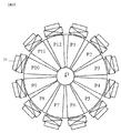
- the structure of the aberration correction multipole element 20 is shown in FIG.
- the 12-pole Wien filter is used as the most effective example.
- This Wien filter extends in a direction parallel to the optical axis O, and has 12 rotationally symmetrical poles P1 to P12 around the optical axis O.
- the poles P1 to P12 are made of magnetic metals such as iron, nickel and permalloy, and can simultaneously generate a magnetic field and an electric field. Furthermore, a 4-pole field and an 8-pole field are simultaneously generated from the relationship between the number of electrodes and the arrangement.
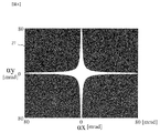
- the amount of wavefront aberration ⁇ when the 8-pole field A3 is generated from the multipole element for correction 20 in order to cancel the spherical aberration Cs generated by the objective lens 21 is shown below.
- Cs spherical aberration amount
- A3 four-time astigmatism
- ⁇ objective lens pupil plane azimuth angle
- FIG. ⁇ is the lens opening angle.
- the aberration generated by the spherical aberration amount Cs is constant in the azimuthal direction, while the four-time astigmatism has anisotropy. Therefore, as shown in FIG. 3, in the x direction (first direction) and the y direction (third direction), the Cs component and the A3 component are just balance aberration ⁇ ⁇ 0, but the direction (second direction) For example, in the 45-degree direction when the x-direction is 0 degree, the Cs component and the A3 component have the same sign, and the amount of aberration is inversely increased. In order to cut this aberration increase region and use only the ideal lens region of ⁇ 0 for beam formation, a stop that physically cuts the primary electron beam is adopted.
- the hole shape of the aberration cut stop 22 is defined by the following equation.
- FIG. 4 shows the hole shape of the aberration cut stop.
- the hole is opened only in a portion near the aberration amount ⁇ 0, so that when the ideal optical axis of the beam is the z direction, it has a shuri shape extending in the x and y directions.
- the area in which the aberration is offset tends to narrow as the distance from the center of the optical axis in the x direction and y direction increases.
- the opening forming member in which the opening is formed in accordance with the shape of the region where the aberration is canceled.
- the opening has a cross-shape in which the width decreases with distance from the center (optical axis), and the intersection of the x-direction edge and y-direction edge of the opening is It is desirable to form so as to be a curve.
- FIG. 5 is a comparison of the beam profile on the sample surface with and without the aberration cut stop.
- the optical system to which the aberration cut stop is applied has lower intensity (I 2 ′ ⁇ I 2 ). This means that the reduction of the aberration relatively increases the high frequency component. Therefore, with the aperture, the beam can be narrowed relatively. This not only makes it possible to improve the resolution when acquiring a sample image, but also improves the contrast and the noise resistance.
- the hole shape determination method is not limited to this as long as it is a shape using a region where the aberration distribution ⁇ 0.
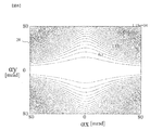
- the chromatic aberration Cc is considered here.
- Negative chromatic aberration is generally obtained by generating both electric and magnetic quadrupole fields.
- the wavefront aberration equation in the case where the spherical surface and the chromatic aberration are corrected by the combination of the octupole and the quadrupole is shown below.
- Cc is the amount of chromatic aberration
- Cc2 is the negative chromatic aberration due to the quadrupole field
- V0 is the acceleration voltage
- ⁇ V is the chromatic dispersion.
- FIG. 6 is an aberration amount distribution in the case where the chromatic aberration is included.
- the chromatic aberration is constant in the azimuthal direction, but the quadrupolar field used for cancellation is a two-fold symmetric field, and in the example, ⁇ x0 only on the x axis.
- FIG. 7 shows the shape of the aperture hole in the case of defining the aberration cut aperture by the aberration allowance b. Since the ⁇ 0 portion is in a direction parallel to the x-axis, it has a laterally elongated hole shape.
- the ideal lens is taken out with the value of b, but the method of determining the hole shape is not limited in consideration of the purpose of removing the influence of aberration by using the ideal lens portion.
- the beam can be compared with a simple circular stop. It is possible to suppress chromatic aberration and spherical aberration while suppressing a decrease in current. If only chromatic aberration is to be corrected, four or more poles are required, and to correct spherical aberration, eight or more poles are required. In addition, since the correction can be performed only by the electric field or the magnetic field if only the spherical aberration is corrected, the aberration corrector can be configured by the magnetic poles or the poles of only the electrodes without using the Wien filter.
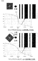
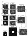
- FIG. 8 is a line pattern sample image in the case of using the beam profile in the case of the presence of the aberration cut stop shown in FIG.
- the sample image is obtained by two-dimensionally scanning the beam on a sample in which a plurality of line patterns are arranged.
- a beam (without beam rotation) having a long beam shape in the x direction and y direction with respect to the other direction is obtained when scanning a sample in which a long line pattern in the y direction is arranged in the x direction And an image obtained by scanning the beam by rotating the longitudinal direction of the beam by 45 degrees. When rotated 45 degrees, the slope of the profile becomes dull with respect to no rotation.
- the long beam in the direction perpendicular to the beam optical axis formed by the aberration cut stop 22 is suppressed in the long direction by the above principle, so the longitudinal direction of the beam cross section and the scanning line direction Can be obtained by scanning such that the scanning line direction and the edge of the pattern are orthogonal to each other, thereby obtaining a signal suitable for measuring the pattern width.
- luminance change information line profile
- dimensions between portions corresponding to edges for example, position 801 in FIG. 8 are measured. Measure the line width, pitch and so on.
- Such processing is performed by the image processing unit 2 or the like based on a predetermined program.
- FIG. 9 is a sample image in the case of scanning the beam with the aberration cut stop shown in FIG. 5 with respect to the round sample. It can be seen that a change in the tailing direction of the sample shape occurs as the beam rotates.
- the sample image captured in each direction is combined and restored based on the optical transfer function (OTF) of the beam while rotating the beam.
- OFT is a response function determined by the beam opening angle and the aberration distribution, and indicates how much frequency information of the sample shape can be held at the time of image formation.
- FIG. 10 is a flow of the combining process.
- a 4/8 pole field that cancels the aberration of the lens of the aberration correction target is generated using the aberration corrector 20 (step 101).
- the number of rotations n is set to zero. is set using, for example, an input device (not shown) connected to the control device 30.
- the 4- and 8-pole fields are calculated based on the following equation, and the voltage applied to each electrode and each magnetic pole is controlled based on the calculation result.
- the direction to cancel the aberration is rotated (step 103). (Potential configuration of electrode)
- [Equation 4] and [Equation 5] respectively indicate voltages applied to the respective poles (kth of P1 to P12 in the case of FIG. 3) in generating a 2 n pole field (condition mmn) in a 2 m multipole element
- Ukx is a voltage configuration when the force for the primary beam acts in the x direction
- Uky is a voltage configuration when the force for the primary beam acts in the y direction
- U is an aberration correction voltage.
- the blending ratio of Ukx and Uky may be determined by the following equation.
- IkxTkx is the magnetic configuration when the force for the primary beam acts in the x direction
- IkyTky is the magnetic configuration when the force for the primary beam acts in the y direction
- IT is the amount of currents and the number of turns used for aberration correction.
- the aperture is also rotated accordingly (step 104).
- a method of mechanically rotating the diaphragm itself, a method of replacing with a different diaphragm, or an electrical method can be considered. If the direction of rotation is determined in advance, a stop hole shape may be adopted in which the shape of the stop hole corresponding to each direction is added.
- a desired sample image ign is imaged (step 105), and its Fourier transform IGn is calculated (step 106).
- the transfer function OTFn of the beam after rotation is also calculated (step 107).
- FIG. 11 is a diagram showing an example of an image obtained in each process of image processing along the flowchart illustrated in FIG. It is understood that an image obtained based on scanning of a beam having anisotropy with respect to a round sample image has tailing depending on the beam profile (brightness distribution obtained when the beam is irradiated). . On the other hand, it can be understood that when the restoration processing is performed, an image in which the anisotropy is eliminated as well as the original image can be obtained.
- the contour of the sample becomes sharper and leads to the improvement of the image quality.
- the optical transfer function OTF is used to improve the image quality of an image acquired by an anisotropically generated beam.
- Booster control section 26 Axillary distribution (spherical aberration only) 27: Aberration cut aperture shape (spherical aberration only) 28: Axle distribution (spherical surface, considering chromatic aberration) 27: Aberration cut aperture shape (spherical surface, considering chromatic aberration), 30 ...Control device
Landscapes
- Chemical & Material Sciences (AREA)
- Analytical Chemistry (AREA)
- Analysing Materials By The Use Of Radiation (AREA)
Abstract
La présente invention a pour objectif d'obtenir un degré élevé de correction d'aberration chromatique, d'aberration sphérique, ou les deux à l'aide d'une configuration et d'un réglage simples. L'invention réalise à cet effet un dispositif de correction d'aberration qui est disposé conjointement avec un élément optique à corriger le long de l'axe optique du faisceau de particules chargées, caractérisé en ce qu'il comprend 2n (n≥2) pôles et un élément de formation d'ouverture ayant une ouverture pour le passage du faisceau de particules chargées. L'ouverture est formée de manière à être comparativement plus longue dans une première direction (telle qu'une direction à 0 degré) que dans une deuxième direction (telle qu'une direction à 45 degrés) qui est orthogonale à l'axe optique, la première direction étant orthogonale à l'axe optique tout en étant différente de la deuxième direction, et la première direction étant en outre une direction le long de laquelle l'aberration générée par le fonctionnement du dispositif de correction d'aberration annule l'aberration générée par ledit élément optique à corriger.
Priority Applications (2)
| Application Number | Priority Date | Filing Date | Title |
|---|---|---|---|
| JP2019532318A JP6777821B2 (ja) | 2017-07-28 | 2017-07-28 | 収差補正装置及び荷電粒子線装置 |
| PCT/JP2017/027414 WO2019021455A1 (fr) | 2017-07-28 | 2017-07-28 | Dispositif de correction d'aberration et dispositif à faisceau de particules chargées |
Applications Claiming Priority (1)
| Application Number | Priority Date | Filing Date | Title |
|---|---|---|---|
| PCT/JP2017/027414 WO2019021455A1 (fr) | 2017-07-28 | 2017-07-28 | Dispositif de correction d'aberration et dispositif à faisceau de particules chargées |
Publications (1)
| Publication Number | Publication Date |
|---|---|
| WO2019021455A1 true WO2019021455A1 (fr) | 2019-01-31 |
Family
ID=65040533
Family Applications (1)
| Application Number | Title | Priority Date | Filing Date |
|---|---|---|---|
| PCT/JP2017/027414 Ceased WO2019021455A1 (fr) | 2017-07-28 | 2017-07-28 | Dispositif de correction d'aberration et dispositif à faisceau de particules chargées |
Country Status (2)
| Country | Link |
|---|---|
| JP (1) | JP6777821B2 (fr) |
| WO (1) | WO2019021455A1 (fr) |
Cited By (1)
| Publication number | Priority date | Publication date | Assignee | Title |
|---|---|---|---|---|
| JP2023122250A (ja) * | 2022-02-22 | 2023-09-01 | 日本電子株式会社 | 収差補正装置および電子顕微鏡 |
Citations (4)
| Publication number | Priority date | Publication date | Assignee | Title |
|---|---|---|---|---|
| JP2004134389A (ja) * | 2002-08-13 | 2004-04-30 | Leo Elektronenmikroskopie Gmbh | ビーム誘導構成体、結像方法、電子顕微鏡システムおよび電子リソグラフィシステム |
| JP2006147520A (ja) * | 2004-10-19 | 2006-06-08 | Jeol Ltd | 収差補正装置及び電子顕微鏡 |
| WO2010035386A1 (fr) * | 2008-09-25 | 2010-04-01 | 株式会社日立ハイテクノロジーズ | Appareil à faisceau de particules chargées et procédé de mesure d'aberration géométrique employé dans celui-ci |
| JP2015207351A (ja) * | 2014-04-17 | 2015-11-19 | 日本電子株式会社 | 多極子レンズ、収差補正装置、および電子顕微鏡 |
-
2017
- 2017-07-28 WO PCT/JP2017/027414 patent/WO2019021455A1/fr not_active Ceased
- 2017-07-28 JP JP2019532318A patent/JP6777821B2/ja not_active Expired - Fee Related
Patent Citations (4)
| Publication number | Priority date | Publication date | Assignee | Title |
|---|---|---|---|---|
| JP2004134389A (ja) * | 2002-08-13 | 2004-04-30 | Leo Elektronenmikroskopie Gmbh | ビーム誘導構成体、結像方法、電子顕微鏡システムおよび電子リソグラフィシステム |
| JP2006147520A (ja) * | 2004-10-19 | 2006-06-08 | Jeol Ltd | 収差補正装置及び電子顕微鏡 |
| WO2010035386A1 (fr) * | 2008-09-25 | 2010-04-01 | 株式会社日立ハイテクノロジーズ | Appareil à faisceau de particules chargées et procédé de mesure d'aberration géométrique employé dans celui-ci |
| JP2015207351A (ja) * | 2014-04-17 | 2015-11-19 | 日本電子株式会社 | 多極子レンズ、収差補正装置、および電子顕微鏡 |
Cited By (3)
| Publication number | Priority date | Publication date | Assignee | Title |
|---|---|---|---|---|
| JP2023122250A (ja) * | 2022-02-22 | 2023-09-01 | 日本電子株式会社 | 収差補正装置および電子顕微鏡 |
| JP7465295B2 (ja) | 2022-02-22 | 2024-04-10 | 日本電子株式会社 | 収差補正装置および電子顕微鏡 |
| US12354827B2 (en) | 2022-02-22 | 2025-07-08 | Jeol Ltd. | Aberration correcting device and electron microscope |
Also Published As
| Publication number | Publication date |
|---|---|
| JP6777821B2 (ja) | 2020-10-28 |
| JPWO2019021455A1 (ja) | 2020-07-02 |
Similar Documents
| Publication | Publication Date | Title |
|---|---|---|
| US9093246B2 (en) | SACP method and particle optical system for performing the method | |
| TWI590286B (zh) | 用於高解析度電子束成像之裝置及方法 | |
| JP6554288B2 (ja) | 荷電粒子線装置 | |
| EP2172960B1 (fr) | Correcteur d'aberrations chromatiques pour système de faisceaux de particules chargées et procédé de correction correspondant | |
| CN112840431A (zh) | 带电粒子束设备、场曲校正器、及操作带电粒子束设备的方法 | |
| EP2020673A2 (fr) | Système de correction d'aberrations | |
| US20080179536A1 (en) | Changed particle beam emitting device and method for adjusting the optical axis | |
| JP6037693B2 (ja) | 荷電粒子線装置 | |
| US11430630B2 (en) | Charged particle beam apparatus | |
| US20180005797A1 (en) | Scanning electron microscope | |
| US8884245B2 (en) | Corrector for the correction of chromatic aberrations in a particle-optical apparatus | |
| US6653632B2 (en) | Scanning-type instrument utilizing charged-particle beam and method of controlling same | |
| US20050189496A1 (en) | Method of automatically correcting aberrations in charged-particle beam and apparatus therefor | |
| JP2014053074A (ja) | 荷電粒子線装置 | |
| WO2019021455A1 (fr) | Dispositif de correction d'aberration et dispositif à faisceau de particules chargées | |
| TWI753374B (zh) | 荷電粒子束裝置 | |
| US20120080594A1 (en) | Particle beam device and method for analyzing and/or treating an object | |
| JP4328192B2 (ja) | 荷電粒子光学系における多極場発生装置および収差補正装置 | |
| WO2021100172A1 (fr) | Dispositif à faisceau de particules chargées et procédé de correction d'aberration | |
| US9991088B2 (en) | Charged particle beam device and aberration corrector | |
| US11043353B2 (en) | Energy filter and charged particle beam apparatus | |
| JP2007287495A (ja) | 2レンズ光学系走査型収差補正集束イオンビーム装置及び3レンズ光学系走査型収差補正集束イオンビーム装置及び2レンズ光学系投影型収差補正イオン・リソグラフィー装置並びに3レンズ光学系投影型収差補正イオン・リソグラフィー装置 | |
| US20250391629A1 (en) | Aberration correction in charged particle spectroscopy | |
| US12340970B2 (en) | Charged particle beam device, and method for controlling charged particle beam device | |
| WO2023139631A1 (fr) | Dispositif à faisceau de particules chargées et procédé de déviation de faisceau dans un dispositif à faisceau de particules chargées |
Legal Events
| Date | Code | Title | Description |
|---|---|---|---|
| 121 | Ep: the epo has been informed by wipo that ep was designated in this application |
Ref document number: 17919057 Country of ref document: EP Kind code of ref document: A1 |
|
| ENP | Entry into the national phase |
Ref document number: 2019532318 Country of ref document: JP Kind code of ref document: A |
|
| NENP | Non-entry into the national phase |
Ref country code: DE |
|
| 122 | Ep: pct application non-entry in european phase |
Ref document number: 17919057 Country of ref document: EP Kind code of ref document: A1 |