WO2019041840A1 - 一种存储单元和静态随机存储器 - Google Patents
一种存储单元和静态随机存储器 Download PDFInfo
- Publication number
- WO2019041840A1 WO2019041840A1 PCT/CN2018/084100 CN2018084100W WO2019041840A1 WO 2019041840 A1 WO2019041840 A1 WO 2019041840A1 CN 2018084100 W CN2018084100 W CN 2018084100W WO 2019041840 A1 WO2019041840 A1 WO 2019041840A1
- Authority
- WO
- WIPO (PCT)
- Prior art keywords
- read
- mos transistor
- line
- bit
- word line
- Prior art date
- Legal status (The legal status is an assumption and is not a legal conclusion. Google has not performed a legal analysis and makes no representation as to the accuracy of the status listed.)
- Ceased
Links
Images


Classifications
-
- G—PHYSICS
- G11—INFORMATION STORAGE
- G11C—STATIC STORES
- G11C11/00—Digital stores characterised by the use of particular electric or magnetic storage elements; Storage elements therefor
- G11C11/21—Digital stores characterised by the use of particular electric or magnetic storage elements; Storage elements therefor using electric elements
- G11C11/34—Digital stores characterised by the use of particular electric or magnetic storage elements; Storage elements therefor using electric elements using semiconductor devices
- G11C11/40—Digital stores characterised by the use of particular electric or magnetic storage elements; Storage elements therefor using electric elements using semiconductor devices using transistors
- G11C11/41—Digital stores characterised by the use of particular electric or magnetic storage elements; Storage elements therefor using electric elements using semiconductor devices using transistors forming static cells with positive feedback, i.e. cells not needing refreshing or charge regeneration, e.g. bistable multivibrator or Schmitt trigger
- G11C11/412—Digital stores characterised by the use of particular electric or magnetic storage elements; Storage elements therefor using electric elements using semiconductor devices using transistors forming static cells with positive feedback, i.e. cells not needing refreshing or charge regeneration, e.g. bistable multivibrator or Schmitt trigger using field-effect transistors only
-
- G—PHYSICS
- G11—INFORMATION STORAGE
- G11C—STATIC STORES
- G11C11/00—Digital stores characterised by the use of particular electric or magnetic storage elements; Storage elements therefor
- G11C11/21—Digital stores characterised by the use of particular electric or magnetic storage elements; Storage elements therefor using electric elements
- G11C11/34—Digital stores characterised by the use of particular electric or magnetic storage elements; Storage elements therefor using electric elements using semiconductor devices
- G11C11/40—Digital stores characterised by the use of particular electric or magnetic storage elements; Storage elements therefor using electric elements using semiconductor devices using transistors
- G11C11/41—Digital stores characterised by the use of particular electric or magnetic storage elements; Storage elements therefor using electric elements using semiconductor devices using transistors forming static cells with positive feedback, i.e. cells not needing refreshing or charge regeneration, e.g. bistable multivibrator or Schmitt trigger
- G11C11/413—Auxiliary circuits, e.g. for addressing, decoding, driving, writing, sensing, timing or power reduction
- G11C11/417—Auxiliary circuits, e.g. for addressing, decoding, driving, writing, sensing, timing or power reduction for memory cells of the field-effect type
- G11C11/418—Address circuits
-
- G—PHYSICS
- G11—INFORMATION STORAGE
- G11C—STATIC STORES
- G11C11/00—Digital stores characterised by the use of particular electric or magnetic storage elements; Storage elements therefor
- G11C11/21—Digital stores characterised by the use of particular electric or magnetic storage elements; Storage elements therefor using electric elements
- G11C11/34—Digital stores characterised by the use of particular electric or magnetic storage elements; Storage elements therefor using electric elements using semiconductor devices
- G11C11/40—Digital stores characterised by the use of particular electric or magnetic storage elements; Storage elements therefor using electric elements using semiconductor devices using transistors
- G11C11/41—Digital stores characterised by the use of particular electric or magnetic storage elements; Storage elements therefor using electric elements using semiconductor devices using transistors forming static cells with positive feedback, i.e. cells not needing refreshing or charge regeneration, e.g. bistable multivibrator or Schmitt trigger
- G11C11/413—Auxiliary circuits, e.g. for addressing, decoding, driving, writing, sensing, timing or power reduction
- G11C11/417—Auxiliary circuits, e.g. for addressing, decoding, driving, writing, sensing, timing or power reduction for memory cells of the field-effect type
- G11C11/419—Read-write [R-W] circuits
-
- G—PHYSICS
- G11—INFORMATION STORAGE
- G11C—STATIC STORES
- G11C7/00—Arrangements for writing information into, or reading information out from, a digital store
- G11C7/10—Input/output [I/O] data interface arrangements, e.g. I/O data control circuits, I/O data buffers
- G11C7/1006—Data managing, e.g. manipulating data before writing or reading out, data bus switches or control circuits therefor
-
- G—PHYSICS
- G11—INFORMATION STORAGE
- G11C—STATIC STORES
- G11C7/00—Arrangements for writing information into, or reading information out from, a digital store
- G11C7/10—Input/output [I/O] data interface arrangements, e.g. I/O data control circuits, I/O data buffers
- G11C7/1015—Read-write modes for single port memories, i.e. having either a random port or a serial port
- G11C7/1045—Read-write mode select circuits
-
- G—PHYSICS
- G11—INFORMATION STORAGE
- G11C—STATIC STORES
- G11C7/00—Arrangements for writing information into, or reading information out from, a digital store
- G11C7/10—Input/output [I/O] data interface arrangements, e.g. I/O data control circuits, I/O data buffers
- G11C7/1075—Input/output [I/O] data interface arrangements, e.g. I/O data control circuits, I/O data buffers for multiport memories each having random access ports and serial ports, e.g. video RAM
-
- G—PHYSICS
- G11—INFORMATION STORAGE
- G11C—STATIC STORES
- G11C7/00—Arrangements for writing information into, or reading information out from, a digital store
- G11C7/12—Bit line control circuits, e.g. drivers, boosters, pull-up circuits, pull-down circuits, precharging circuits, equalising circuits, for bit lines
-
- G—PHYSICS
- G11—INFORMATION STORAGE
- G11C—STATIC STORES
- G11C7/00—Arrangements for writing information into, or reading information out from, a digital store
- G11C7/18—Bit line organisation; Bit line lay-out
-
- G—PHYSICS
- G11—INFORMATION STORAGE
- G11C—STATIC STORES
- G11C8/00—Arrangements for selecting an address in a digital store
- G11C8/08—Word line control circuits, e.g. drivers, boosters, pull-up circuits, pull-down circuits, precharging circuits, for word lines
-
- G—PHYSICS
- G11—INFORMATION STORAGE
- G11C—STATIC STORES
- G11C8/00—Arrangements for selecting an address in a digital store
- G11C8/14—Word line organisation; Word line lay-out
-
- G—PHYSICS
- G11—INFORMATION STORAGE
- G11C—STATIC STORES
- G11C8/00—Arrangements for selecting an address in a digital store
- G11C8/16—Multiple access memory array, e.g. addressing one storage element via at least two independent addressing line groups
-
- Y—GENERAL TAGGING OF NEW TECHNOLOGICAL DEVELOPMENTS; GENERAL TAGGING OF CROSS-SECTIONAL TECHNOLOGIES SPANNING OVER SEVERAL SECTIONS OF THE IPC; TECHNICAL SUBJECTS COVERED BY FORMER USPC CROSS-REFERENCE ART COLLECTIONS [XRACs] AND DIGESTS
- Y02—TECHNOLOGIES OR APPLICATIONS FOR MITIGATION OR ADAPTATION AGAINST CLIMATE CHANGE
- Y02D—CLIMATE CHANGE MITIGATION TECHNOLOGIES IN INFORMATION AND COMMUNICATION TECHNOLOGIES [ICT], I.E. INFORMATION AND COMMUNICATION TECHNOLOGIES AIMING AT THE REDUCTION OF THEIR OWN ENERGY USE
- Y02D10/00—Energy efficient computing, e.g. low power processors, power management or thermal management
Definitions
- the present invention relates to the field of storage, and in particular, to a storage unit and a static random access memory (SRAM).
- SRAM static random access memory
- FIG. 1 is a schematic structural diagram of a memory cell of a conventional SRAM.
- the memory cell adopts an ordinary six-tube unit composed of six metal oxide semiconductor (MOS) field effect transistors, and the MOS field effect transistor is simply referred to as a MOS transistor.
- the memory cell includes two inverting gates and two MOS transistors. Among them, two inverting gates are composed of four MOS tubes, and two inverting gates in the figure constitute a latch for storing data, and two MOS tubes in the figure are used for gated access. There are two stable states, 0 and 1, for the latch connected by two inverting gate loops. Wherein, A and B are two oppositely stored memory bits.
- bit_line WL
- bit line bit_line, BL
- Read Pull WL high and read the bit from BL.
- Write Pull WL high, pull high or pull BL low, because BL's driving ability is stronger than the memory unit, it will force to cover the original state.
- both bit and nbit represent bit lines, bit line bits are used to read the data of the memory bit A, and bit line nbit is used to read the data of the memory bit B, and the data of the memory cells read by the two are opposite.
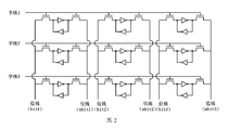
- FIG. 2 is a schematic diagram of a conventional SRAM memory array.
- the memory array includes 3 x 3 of memory cells as shown in FIG.
- Embodiments of the present invention provide a storage unit and a static random access memory, which can implement reading of a read word line and a read bit line, thereby being able to acquire data of a certain address with respect to a diagonally symmetric address of the matrix, which is fast. And power consumption and workload are low.
- a memory unit including a latch, the latch providing a first memory bit; the memory unit further comprising a first MOS transistor; a gate of the first MOS transistor The first storage bit is connected to the first storage bit, the source of the first MOS transistor is connected to the first read line, and the drain of the first MOS transistor is connected to the second read line; in the first state, the first a read line is a read word line, and the second read line is a read bit line; in the second state, the second read line is a read word line, and the first read line is Read the bit line.
- a MOS transistor is added, and a gate of the MOS transistor is connected to a storage bit, and a source and a drain of the MOS transistor are respectively connected to the first
- the read line and the second read line are based on the characteristics of the MOS transistor itself, and any one of the first read line and the second read line can be used as a read bit line, and the other is used as a read word line, thereby realizing
- the read word line and the read bit line are interchangeable, and by changing the bottommost hardware storage unit, it is possible to quickly acquire data of a certain address with respect to a diagonally symmetric address of the matrix, instead of writing an algorithm at the code level,
- writing algorithms in the code of a digital circuit can greatly increase the speed and greatly reduce power consumption and workload, usually one to two beats (clock cycle), and digital circuit code Implementation may take thousands of beats.
- the first MOS transistor is an NMOS transistor or a PMOS transistor.
- the latch further provides a second storage bit;
- the storage unit further includes a second MOS transistor; a gate of the second MOS transistor is connected to the second storage bit, A source of the second MOS transistor is connected to the first read line, and a drain of the second MOS transistor is connected to the second read line.
- the data of the two storage bits having the opposite states are respectively read by the pair of MOS transistors, so that the accuracy of reading the data can be improved.
- the first MOS transistor is an NMOS transistor and the second MOS transistor is a PMOS transistor; or the first MOS transistor is a PMOS transistor and the second MOS transistor is an NMOS transistor .
- a static random access memory comprising: a plurality of memory cells; the memory cell comprising a latch, the latch providing a first memory bit; the memory cell further comprising a first MOS transistor; a gate of the first MOS transistor is connected to the first storage bit, a source of the first MOS transistor is connected to a first read line, and a drain of the first MOS transistor is connected to a second Reading the line; in the first state, the first read line is a read word line, the second read line is a read bit line; in the second state, the second read line is Reading a word line, the first read line is a read bit line; the plurality of memory cells form a rectangular memory array having the same number of rows and columns; the memory cells of the same row in the memory array are connected to the same The first read line; the memory cells of the same column in the memory array are connected to the same second read line.
- a memory cell of a static random access memory is based on a structure of a conventional latch capable of providing a memory bit, and a MOS transistor is added, and a gate of the MOS transistor is connected to a memory bit, and a source of the MOS transistor The drains are respectively connected to the first read line and the second read line. Based on the characteristics of the MOS transistor itself, any one of the first read line and the second read line can be used as the read bit line, and the other is read.
- the word line is taken to realize the interchangeability between the read word line and the read bit line, and the bottommost hardware storage unit is changed to quickly acquire data of a certain address about the diagonal symmetric address of the matrix, instead of the code.
- the layer write algorithm which is equivalent to a hardware accelerator, can greatly increase the speed and greatly reduce the power consumption and workload compared to writing algorithms in the code of digital circuits, usually one to two beats (clock cycle). This is done, and digital circuit code implementations may require thousands of beats.
- the first MOS transistor is an NMOS transistor or a PMOS transistor.
- the latch further provides a second storage bit;
- the storage unit further includes a second MOS transistor; a gate of the second MOS transistor is connected to the second storage bit, A source of the second MOS transistor is connected to the first read line, and a drain of the second MOS transistor is connected to the second read line.
- the data of the two storage bits having the opposite states are respectively read by the pair of MOS transistors, so that the accuracy of reading the data can be improved.
- the first MOS transistor is an NMOS transistor and the second MOS transistor is a PMOS transistor; or the first MOS transistor is a PMOS transistor and the second MOS transistor is an NMOS transistor .
- each of the storage units is connected to a control signal; when the control signal is a first sequence, the storage unit is regarded as the first state; when the control signal In the second sequence, the memory unit is considered to be the second state. According to this embodiment, switching of the read state of the memory cell of the static random access memory by the control signal is simple and fast.
- the first sequence has a length of 1 bit; the second sequence has a length of 1 bit; the first sequence is 0 and the second sequence is 1, or the A sequence is 1 and the second sequence is 0.
- switching of the read state of the memory cells of the static random access memory by the 1-bit control signal is simple and fast.
- the static random access memory further includes: a first decoder, a second decoder, a first word line driver, a second word line driver, a first sense amplifier, and a second sense amplifier And an inverter; the control signal is coupled to an enable end of the first decoder, an enable end of the first word line driver, and an enable end of the first sense amplifier; the first decoding The input end of the device inputs an address value, the first output end of the first decoder outputs a line number, and the second output end of the first decoder outputs a column number; the first output end of the first decoder is connected a control end of the first sense amplifier, an input end of the first sense amplifier is connected to the first read line; a second output end of the first decoder is connected to the first word line driver a control terminal, an output end of the first word line driver is connected to the second read line, and a control end of the first sense amplifier is configured to control the first sense amplifier to amplify data of at least one input
- two sets of decoders, word line drivers and sense amplifiers are provided, and the connections of the two sets of decoders, word line drivers and sense amplifiers are different, and a set of decoders and word line drivers are controlled by the control signals.
- the sense amplifier works to achieve the interchange of the read word line and the read bit line.
- the static random access memory further includes: a decoder, a word line driver, a sense amplifier, the same number of first selectors as the number of rows of the storage array, and the storage array The number of columns is the same number of second selectors; the input of the decoder inputs an address value, the first output of the decoder outputs a line number, and the second output of the decoder outputs a column number; the decoding The first output end of the device is connected to the control end of the word line driver, and the control end of the word line driver is configured to control at least one output end of the word line driver to output a first logic state, the second of the decoder An output terminal is connected to the control terminal of the sense amplifier, and a control terminal of the sense amplifier is configured to control the sense amplifier to amplify data of at least one input terminal; the control signal is connected to the first selector and a control end of the second selector; a first port of the first selector is connected to the first read line, a second
- a chip comprising: the static random access memory of the second aspect above.
- the chip is used for convolution kernel decomposition in a convolutional neural network.
- FIG. 1 is a schematic structural diagram of a memory cell of a conventional SRAM
- FIG. 2 is a schematic diagram of a storage array of a conventional SRAM
- FIG. 3 is a schematic structural diagram of a storage unit of an SRAM according to an embodiment of the present invention.
- FIG. 4 is a schematic structural diagram of another storage unit of an SRAM according to an embodiment of the present invention.
- FIG. 5 is a schematic structural diagram of another storage unit of an SRAM according to an embodiment of the present disclosure.
- FIG. 6 is a schematic diagram of reading a storage unit during a conventional reading according to an embodiment of the present invention.
- FIG. 7 is a schematic diagram of reading a storage array during conventional reading according to an embodiment of the present invention.
- FIG. 8 is a schematic diagram of reading a storage unit during a read sequence according to an embodiment of the present invention.
- FIG. 9 is a schematic diagram of reading a storage array during a read sequence according to an embodiment of the present invention.
- FIG. 10 is a schematic diagram of a control circuit according to an embodiment of the present invention.
- FIG. 11 is a schematic diagram of another control circuit according to an embodiment of the present invention.
- Figure 12 is a schematic diagram of an image matrix and a convolution kernel matrix
- Figure 13 is a schematic diagram of convolution calculation between a 5 x 5 image matrix and a 3 x 3 convolution kernel matrix.
- Embodiments of the present invention provide a memory unit including a latch, the latch providing a first storage bit; the memory unit further includes a first MOS transistor; and the first MOS transistor a gate is connected to the first storage bit, a source of the first MOS transistor is connected to a first read line, and a drain of the first MOS transistor is connected to a second read line; in the first state, the The first read line is a read word line, and the second read line is a read bit line; in the second state, the second read line is a read word line, the first read line To read the bit line.
- the latch may be, but not limited to, a latch formed by cyclically connecting two inverting gates. Based on the latches included in a typical memory cell, the original bit lines and word lines corresponding to the latch are no longer used to read data.
- the first MOS transistor can be an NMOS transistor or a PMOS transistor.
- the latch further provides a second memory bit;
- the memory cell further includes a second MOS transistor; a gate of the second MOS transistor is coupled to the second memory bit, the second MOS A source of the tube is coupled to the first read line, and a drain of the second MOS tube is coupled to the second read line.
- the data of the two storage bits having the opposite states are respectively read by the pair of MOS transistors, so that the accuracy of reading the data can be improved.
- the first MOS transistor is an NMOS transistor and the second MOS transistor is a PMOS transistor; or the first MOS transistor is a PMOS transistor and the second MOS transistor is an NMOS transistor.
- a MOS transistor is added, and a gate of the MOS transistor is connected to a storage bit, and a source and a drain of the MOS transistor are respectively connected to the first
- the read line and the second read line are based on the characteristics of the MOS transistor itself, and any one of the first read line and the second read line can be used as a read bit line, and the other is used as a read word line, thereby realizing
- the read word line and the read bit line are interchangeable, and by changing the bottommost hardware storage unit, it is possible to quickly acquire data of a certain address with respect to a diagonally symmetric address of the matrix, instead of writing an algorithm at the code level,
- writing algorithms in the code of a digital circuit can greatly increase the speed and greatly reduce power consumption and workload, usually one to two beats (clock cycle), and digital circuit code Implementation may take thousands of beats.
- FIG. 3 is a schematic structural diagram of a storage unit of an SRAM according to an embodiment of the present invention. If the two reverse gates are designed according to the structure of the four MOS tubes of the prior art, the memory unit in the embodiment of the present invention can be regarded as a 7-tube unit, and one of the conventional 6-tube units is added.
- the MOS tube in the circle as shown in the figure makes the SRAM have two modes of conventional reading and sequential reading.
- the structure of the memory cell shown in FIG. 3 is specifically described below.
- the memory cell includes: a first MOS transistor, a second MOS transistor, a third MOS transistor, a fourth MOS transistor, a fifth MOS transistor 31, and a sixth MOS tube 32 (fifth MOS tube, sixth MOS tube is also called write MOS tube) and seventh MOS tube 33;
- the first MOS transistor, the second MOS transistor, the third MOS transistor, and the fourth MOS transistor are not shown in FIG. 3, and the first MOS transistor and the second MOS transistor constitute a first inversion gate 34, The third MOS transistor and the fourth MOS transistor constitute a second inverting gate 35; the first inverting gate 34 and the second inverting gate 35 are connected end to end to form a latch, the first counter
- the output of the phase gate 34 is the first storage bit Q
- the output of the second inverter gate 35 is the second storage bit.
- WWL write word line
- WBL write bit line negate
- the first write bit line is denoted as WBL
- the second write bit line is denoted as WBLN
- the fifth MOS transistor 31 and the sixth MOS transistor are made through the write word line 32 is turned on, for example, the write word line WWL is logic 1
- the logic state of the first write bit line WBL is a logic state of the data
- the data is written into the second memory bit
- the logic state of the second write bit line WBLN is the logic state of the data, the data is written into the first storage bit Q;
- the first state and the second state are only used to distinguish two different read states, and the first state and the second state are not limited in the embodiment of the present invention.
- the first read line in the first state, is a read word line, the second read line is a read bit line; in the second state, the second read line is a read a word line, the first read line being a read bit line.
- the second read line is a read word line, the first read line is a read bit line; in the second state, the first read line is a read A word line is taken, and the second read line is a read bit line.
- a gate of the seventh MOS transistor 33 is connected to the first storage bit Q and the second storage bit
- One of the storage bits, one of the source and the drain of the seventh MOS transistor 33 is connected to the first read line L1, and the other of the source and the drain of the seventh MOS transistor 33 is connected a second read line L2;
- the first read line L1 is a read bit line (RBL_H, wherein H is used to identify the first read state, first The read state may be referred to as a first state
- the second read line L2 is a read word line (RWL_H);
- the first read line L1 is Reading a word line (RWL_V, wherein V is used to identify a second read state, the second read state may be simply referred to as a second state), and the second read line L2 is a read bit line (RBL_V);
- the read word line RWL_H or RWL_V
- the first read state may be referred to as a conventional read
- the second read state may be referred to as a sequential read.
- WBL and WBLN are two positive and negative write bit lines for writing stored data; WWL is a write word for gated access when writing data; RBL_H is a read bit line for conventional reading, for Read the stored data; RWL_H is the read word line for the conventional read, and is used to read the gated access when the data is stored; RWL_V is the read word line when the read data is read, and is used to read the stored data.
- RBL_V is the read bit line when reading in reverse order, used to read the stored data
- the read bit line in the traditional read is the read word line when the read is read, in the traditional read
- the read word line is the read bit line when it is read in sequence
- Q For the storage bit.
- the peripheral circuit can be set with a 1-bit control signal, such as T_EN, and the read mode is controlled by T_EN for conventional read or sequential read.
- the seventh MOS transistor 33 is an NMOS transistor.
- the seventh MOS transistor 33 of FIG. 3 can also be replaced with a PMOS transistor, such as the memory cell shown in FIG.
- a MOS transistor such as the memory cell shown in FIG. 5, may be added to the memory cell shown in FIG. 3 or FIG.
- the memory unit further includes an eighth MOS transistor 36; a gate of the eighth MOS transistor 36 is connected to the first storage bit Q and the second storage bit Another memory bit (for example, when the seventh MOS transistor 33 is connected to the first memory bit Q, the eighth MOS transistor 36 is connected to the second memory bit One of the source and the drain of the eighth MOS transistor 36 is connected to the first read line L1, and the other of the source and the drain of the eighth MOS transistor 36 is connected to the a second read line L2 (for example, a source of the eighth MOS transistor 36 is connected to the first read line L1, and a drain of the eighth MOS transistor 36 is connected to the second read line L2); referring to FIG.
- the seventh MOS transistor 33 is a PMOS transistor and the eighth MOS transistor 36 is an NMOS transistor. It can be understood that the seventh MOS transistor 33 is an NMOS transistor and the eighth MOS transistor 36 is a PMOS transistor. . According to this embodiment, the data of the two storage bits having the opposite states are respectively read by the pair of MOS transistors, so that the accuracy of reading the data can be improved.
- the storage unit is connected to the control signal; when the control signal is in the first sequence, the storage unit is in the first read state, that is, L1 is a read bit line. L2 is a read word line, and the control circuit controls the peripheral circuit to pull the level of L2 to read data from L1; when the control signal is the second sequence, the memory unit is in the second The read state, that is, L1 is the read word line, and L2 is the read bit line.
- the control circuit controls the peripheral circuit to pull up the level of L1, and the data can be read from L2. According to this embodiment, switching of the read state of the memory cell is controlled by the control signal, which is simple and fast.
- the first sequence has a length of 1 bit; the second sequence has a length of 1 bit; the first sequence is 0 and the second sequence is 1, or the A sequence is 1 and the second sequence is 0.
- switching of the read state of the memory cell by the 1-bit control signal is simple and fast.
- the embodiment of the present invention further provides a static random access memory, where the static random access memory includes: a plurality of foregoing storage units (for example, the storage unit shown in FIG. 3, FIG. 4 or FIG. 5);
- the storage unit constitutes a rectangular storage array having the same number of rows and columns; the storage units of the same row in the storage array have the same first read line; the storage units of the same column in the storage array have the same second Read the line.
- the static random access memory includes: a plurality of foregoing storage units (for example, the storage unit shown in FIG. 3, FIG. 4 or FIG. 5);
- the storage unit constitutes a rectangular storage array having the same number of rows and columns; the storage units of the same row in the storage array have the same first read line; the storage units of the same column in the storage array have the same second Read the line.
- the storage unit of the static random access memory is based on the structure of the conventional memory unit, and a MOS transistor is added.
- the newly added MOS transistor is the seventh MOS transistor, because the gate of the seventh MOS transistor Connecting a storage bit, the source and the drain of the seventh MOS transistor are respectively connected to the first read line and the second read line, and based on characteristics of the MOS tube itself, in the first read line and the second read line Either one can be used as a read bit line, and the other can be used as a read word line, thereby realizing interchangeability between the read word line and the read bit line.
- a fast acquisition of an address can be realized.
- Data about diagonally symmetric addresses of a matrix, rather than writing algorithms at the code level, is equivalent to a hardware accelerator, which can greatly increase the speed compared to writing algorithms in the code of a digital circuit, usually one to two beats (clock Cycles can be done, and digital circuit code implementations can take thousands of beats and dramatically reduce power consumption and workload.
- each of the memory cells is coupled to a control signal; when the control signal is in a first sequence, the memory cell is in the first read state; and when the control signal is in a second sequence The memory unit is in the second read state. According to this embodiment, switching of the read state of the memory cells of the static random access memory by the control signal is simple and fast.
- the first sequence has a length of 1 bit; the second sequence has a length of 1 bit; the first sequence is 0 and the second sequence is 1, or the first sequence is 1 And the second sequence is zero.
- switching of the read state of the memory cells of the static random access memory by the 1-bit control signal is simple and fast.
- only the control signal is 1 bit as an example for description.
- FIG. 6 is a schematic diagram of memory cell reading during conventional reading.
- the SRAM reading mode is conventional reading: the vertical reading bit is Line RBL_H, traversing is the read word line RWL_H.
- the read word line RWL_H is kept at 1, if the value stored in the node Q is 0, the added MOS transistor is turned off, then the data read from the read bit line RBL_H is 0; if the value stored in the node Q is 1, the added When the MOS transistor is turned on, the data read from the read bit line RBL_H is 1.
- FIG. 7 is a schematic diagram of memory array reading during conventional reading. Assuming that the data stored in the memory cell with the word line number 0 and the bit line number 2 is read, the data of (RBL_H2, RWL_H0), that is, the data of the rightmost memory cell of the first row is read.
- FIG. 8 is a schematic diagram of memory cell reading during sequential read.
- the SRAM read mode is read in sequence: the horizontal becomes read
- the bit line RBL_V is taken up and becomes the read word line RWL_V.
- the value of the word line and the bit line sent from the outside is not changed, but the word line bit line itself is changed, that is, the word line bit line is interchanged.
- FIG. 9 is a schematic diagram of the storage array reading during the sequential reading. It is assumed that the data stored in the memory cell with the word line number 0 and the bit line number 2 is still to be read, but as shown in FIG.
- the data of (RBL_V2, RWL_V0) is read, that is, the lowermost memory cell of the first column.
- the stored data that is, the data of the storage unit of the conventionally read storage unit in Fig. 7 with respect to the diagonally symmetric position of the matrix. In this way, only one beat (ie, one clock cycle) can be used to read data of a storage address with respect to the diagonally symmetric storage address of the storage array, thereby greatly improving the speed and greatly reducing power consumption. And the workload.
- each of the storage units is connected to a control signal; when the control signal is in a first sequence, the storage unit is in the first read state; when the control signal In the second sequence, the memory unit is in the second read state. According to this embodiment, switching of the read state of the memory cells of the static random access memory by the control signal is simple and fast.
- the first sequence has a length of 1 bit; the second sequence has a length of 1 bit; the first sequence is 0 and the second sequence is 1, or the A sequence is 1 and the second sequence is 0.
- switching of the read state of the memory cells of the static random access memory by the 1-bit control signal is simple and fast.
- the switching of the static random access memory between the first read state and the second read state may be implemented by controlling a control circuit at the periphery of the storage array by a control signal.
- FIG. 10 is a schematic diagram of a control circuit according to an embodiment of the present invention.
- the static random access memory further includes a control circuit having the following structure in addition to the storage array: a first decoder 1001, a second decoder 1002, and a first word line driver 1003.
- a second word line driver 1004 a first sense amplifier 1005, a second sense amplifier 1006, and an inverter 1007;
- the control signal T_EN is coupled to the enable end (a1) of the first decoder 1001, the An enable terminal (a1) of the first word line driver 1003 and an enable terminal (a1) of the first sense amplifier 1005;
- an input terminal (a2) of the first decoder 1001 inputs an address value, the a first output end (a3) of a decoder 1001 outputs a line number, a second output end (a4) of the first decoder 1001 outputs a column number; and a first output end (a3) of the first decoder 1001
- Connecting the control terminal (a3) of the first sense amplifier 1005, the input terminals (a10, a11, a12) of the first sense amplifier 1005 are connected to the first read line (ie, the vertical line L10, L11, L12);
- the second output terminal (a4) of the first decoder 1001 is connected to
- two sets of decoders, word line drivers and sense amplifiers are provided, and the connections of the two sets of decoders, word line drivers and sense amplifiers are different, and a set of decoders and word line drivers are controlled by the control signals.
- the sense amplifier works to achieve the interchange of the read word line and the read bit line.
- FIG. 11 is a schematic diagram of another control circuit according to an embodiment of the present invention.
- the static random access memory includes a control circuit including a decoder 1101, a word line driver 1102, a sense amplifier 1103, and the The number of rows of the storage array is the same number of first selectors 1104, the same number of second selectors 1105 as the number of columns of the storage array; the input end (c1) of the decoder 1101 inputs an address value, the decoder a first output end (c2) of 1101 outputs a line number, a second output end (c3) of the decoder 1101 outputs a column number; a first output end (c2) of the decoder 1101 is connected to the word line driver 1102 Control terminal (c2), the control terminal (c2) of the word line driver 1102 is configured to control at least one output terminal (c10, c11, c12) of the word line driver 1102 to output a logic 1, the decoder 1101 a second output terminal (c3) is coupled to the control
- the static random access memory may be disposed in a chip having a specific function, or may be independent of the above chip.
- the above chip can be a chip that requires a large amount of fast matrix calculation.
- custom SRAM in the Convolutional Neural Network (CNN) chip can quickly decompose the convolution kernel.
- the SRAM in the embodiment of the present invention can also be used as an SRAM of some encryption chips.
- CNN With the intelligentization of the chip, based on the standard single instruction multiple data (SIMD), CNN can further reduce the data communication on the bus due to its special multiplexing mechanism.
- SIMD single instruction multiple data
- the concept of reuse is particularly important in very large neural networks.
- the parameter size of the convolution kernel can be as large as 3 ⁇ 3 ⁇ 512, and it is a problem worthy of study to reasonably decompose these super large convolutions into effective hardware.
- the SRAM that can be read in the embodiment of the present invention can eliminate the extra data in the convolution network, and reduce the CNN. Handling power consumption and providing ideas on the underlying hardware for large convolutional structures.
- Convolutional networks are named for "convolution" operations.
- the fundamental purpose of convolution is to extract features from the input image.
- Convolution uses a small square matrix of data to learn image features that preserve the spatial relationship between pixels.
- each picture is a matrix of pixel values.
- the matrix on the left in Figure 12 is the image matrix, which is a special case of the grayscale image (the pixel value of the conventional grayscale image is 0-255).
- the matrix on the right is a convolution kernel matrix, which is a 3 x 3 matrix.
- FIG. 13 is a schematic diagram of convolution calculation between a 5 ⁇ 5 image matrix and a 3 ⁇ 3 convolution kernel matrix: each 3 ⁇ 3 submatrix in the left image matrix is multiplied by a 3 ⁇ 3 convolution kernel matrix, and then The sum obtained by summing the results of the respective positions is placed in a new matrix, that is, the matrix on the right side of Fig. 13, which is a new image matrix generated after the convolution operation of the original image matrix and the convolution kernel matrix.
- the 3x3 matrix in Fig. 12 and Fig. 13 is also called “filter”, “convolution kernel” or “feature detector”.
- the matrix obtained by sliding the filter and the dot multiplication matrix on the original image is called “convolution feature”, " Incentive Mapping or Feature Mapping.
- the filter is a feature detector for the original input picture. Considering the picture as a matrix, after convolving with different convolution kernel matrices, a new picture will be obtained, and different convolution kernel matrices will have different effects.
- Convolution kernel decomposition for example, decomposes a 2-dimensional convolution kernel with respect to diagonal symmetry into two one-dimensional convolution kernels.
- the convolution (set to C) of the image matrix (set to A) and a two-dimensional convolution kernel matrix can be approximated by an image matrix and two one-dimensional convolution kernel matrices (set to S1, S2) for convolutional calculations. ,which is:
- S1 and S2 Equivalent to the two-dimensional convolution kernel C as S1 and S2 is called the decomposition of the convolution kernel, and S1 and S2 are one-dimensional matrices symmetrically about the two-dimensional matrix C diagonally.
Landscapes
- Engineering & Computer Science (AREA)
- Microelectronics & Electronic Packaging (AREA)
- Computer Hardware Design (AREA)
- Multimedia (AREA)
- Static Random-Access Memory (AREA)
- Image Analysis (AREA)
- Life Sciences & Earth Sciences (AREA)
- Biomedical Technology (AREA)
- General Health & Medical Sciences (AREA)
- Molecular Biology (AREA)
- Neurology (AREA)
- Health & Medical Sciences (AREA)
- Semiconductor Memories (AREA)
Abstract
Description
Claims (13)
- 一种存储单元,其特征在于,所述存储单元包括锁存器,所述锁存器提供第一存储位;所述存储单元还包括第一MOS管;所述第一MOS管的栅极连接所述第一存储位,所述第一MOS管的源极连接第一读取线,所述第一MOS管的漏极连接第二读取线;在第一状态下,所述第一读取线为读取字线,所述第二读取线为读取位线;在第二状态下,所述第二读取线为读取字线,所述第一读取线为读取位线。
- 如权利要求1所述的存储单元,其特征在于,所述第一MOS管为NMOS管或PMOS管。
- 如权利要求2所述的存储单元,其特征在于,所述锁存器还提供第二存储位;所述存储单元还包括第二MOS管;所述第二MOS管的栅极连接所述第二存储位,所述第二MOS管的源极连接所述第一读取线,所述第二MOS管的漏极连接所述第二读取线。
- 如权利要求3所述的存储单元,其特征在于,所述第一MOS管为NMOS管且所述第二MOS管为PMOS管;或,所述第一MOS管为PMOS管且所述第二MOS管为NMOS管。
- 一种静态随机存储器,其特征在于,所述静态随机存储器包括:多个存储单元;所述存储单元包括锁存器,所述锁存器提供第一存储位;所述存储单元还包括第一MOS管;所述第一MOS管的栅极连接所述第一存储位,所述第一MOS管的源极连接第一读取线,所述第一MOS管的漏极连接第二读取线;在第一状态下,所述第一读取线为读取字线,所述第二读取线为读取位线;在第二状态下,所述第二读取线为读取字线,所述第一读取线为读取位线;所述多个存储单元构成行列数相同的矩形的存储阵列;所述存储阵列中同一行的所述存储单元连接相同的所述第一读取线;所述存储阵列中同一列的所述存储单元连接相同的所述第二读取线。
- 如权利要求5所述的静态随机存储器,其特征在于,所述第一MOS管为NMOS管或PMOS管。
- 如权利要求6所述的静态随机存储器,其特征在于,所述锁存器还提供第二存储位;所述存储单元还包括第二MOS管;所述第二MOS管的栅极连接所述第二存储位,所述第二MOS管的源极连接所述第一读取线,所述第二MOS管的漏极连接所述第二读取线。
- 如权利要求7所述的静态随机存储器,其特征在于,所述第一MOS管为NMOS管且所述第二MOS管为PMOS管;或,所述第一MOS管为PMOS管且所述第二MOS管为NMOS管。
- 如权利要求5至8中任一项所述的静态随机存储器,其特征在于,每个所述存储单元与控制信号相连接;当所述控制信号为第一序列时,将所述存储单元视为所述第一状态;当所述控制信号为第二序列时,将所述存储单元视为所述第二状态。
- 如权利要求9所述的静态随机存储器,其特征在于,所述第一序列的长度为1bit; 所述第二序列的长度为1bit;所述第一序列为0且所述第二序列为1,或,所述第一序列为1且所述第二序列为0。
- 如权利要求9或10所述的静态随机存储器,其特征在于,所述静态随机存储器还包括:第一解码器、第二解码器、第一字线驱动器、第二字线驱动器、第一读出放大器、第二读出放大器和反相器;所述控制信号连接所述第一解码器的使能端、所述第一字线驱动器的使能端和所述第一读出放大器的使能端;所述第一解码器的输入端输入地址值,所述第一解码器的第一输出端输出行号,所述第一解码器的第二输出端输出列号;所述第一解码器的第一输出端连接所述第一读出放大器的控制端,所述第一读出放大器的输入端连接所述第一读取线;所述第一解码器的第二输出端连接所述第一字线驱动器的控制端,所述第一字线驱动器的输出端连接所述第二读取线,所述第一读出放大器的控制端用于控制所述第一读出放大器对至少一个输入端的数据进行放大处理,所述第一字线驱动器的控制端用于控制所述第一字线驱动器的至少一个输出端输出第一逻辑状态;所述控制信号连接所述反相器的输入端,所述反相器的输出端连接所述第二解码器的使能端、所述第二字线驱动器的使能端和所述第二读出放大器的使能端;所述第二解码器的输入端输入地址值,所述第二解码器的第一输出端输出行号,所述第二解码器的第二输出端输出列号;所述第二解码器的第一输出端连接所述第二读出放大器的控制端,所述第二读出放大器的输入端连接所述第二读取线;所述第二解码器的第二输出端连接所述第二字线驱动器的控制端,所述第二字线驱动器的输出端连接所述第一读取线,所述第二读出放大器的控制端用于控制所述第二读出放大器对至少一个输入端的数据进行放大处理,所述第二字线驱动器的控制端用于控制所述第二字线驱动器的至少一个输出端输出所述第一逻辑状态。
- 如权利要求9或10所述的静态随机存储器,其特征在于,所述静态随机存储器还包括:解码器、字线驱动器、读出放大器、与所述存储阵列的行数相同数目个第一选择器、与所述存储阵列的列数相同数目个第二选择器;所述解码器的输入端输入地址值,所述解码器的第一输出端输出行号,所述解码器的第二输出端输出列号;所述解码器的第一输出端连接所述字线驱动器的控制端,所述字线驱动器的控制端用于控制所述字线驱动器的至少一个输出端输出第一逻辑状态,所述解码器的第二输出端连接所述读出放大器的控制端,所述读出放大器的控制端用于控制所述读出放大器对至少一个输入端的数据进行放大处理;所述控制信号连接所述第一选择器和所述第二选择器的控制端;所述第一选择器的第一端口连接所述第一读取线,所述第一选择器的第二端口连接所述第二读取线,所述第一选择器的第三端口连接所述字线驱动器的输出端;其中,所述第一选择器的控制端用于控制所述第一选择器的第一端口与所述第一选择器的第三端口联通,或所述第一选择器的第二端口与所述第一选择器的第三端口联通;所述第二选择器的第一端口连接所述第二读取线,所述第二选择器的第二端口连接所 述第一读取线,所述第二选择器的第三端口连接所述读出放大器的输入端;其中,所述第二选择器的控制端用于控制所述第二选择器的第一端口与所述第二选择器的第三端口联通,或所述第二选择器的第二端口与所述第二选择器的第三端口联通。
- 一种存储单元,其特征在于,包括锁存器、写MOS管、写字线、写位线、第一读取线和第二读取线,所述锁存器提供第一存储位和第二存储位,所述写位线通过所述写MOS管与所述第一存储位和所述第二存储位相接,所述写字线与所述写MOS管的栅极相连以控制所述写MOS管的导通和关断,所述存储单元还包括第一MOS管,所述第一MOS管的栅极连接所述第一存储位,所述第一MOS管的源极连接所述第一读取线,所述第一MOS管的漏极连接所述第二读取线。
Priority Applications (6)
| Application Number | Priority Date | Filing Date | Title |
|---|---|---|---|
| KR1020207008686A KR20200041989A (ko) | 2017-09-04 | 2018-04-23 | 메모리 유닛 및 정적 랜덤 액세스 메모리 |
| KR1020227025331A KR20220108197A (ko) | 2017-09-04 | 2018-04-23 | 메모리 유닛 및 정적 랜덤 액세스 메모리 |
| EP18849945.3A EP3667669B1 (en) | 2017-09-04 | 2018-04-23 | Memory unit and static random access memory |
| JP2020512869A JP6919950B2 (ja) | 2017-09-04 | 2018-04-23 | 記憶ユニットおよびスタティックランダムアクセスメモリ |
| US16/807,594 US11004502B2 (en) | 2017-09-04 | 2020-03-03 | Storage unit and static random access memory |
| US17/226,614 US11475943B2 (en) | 2017-09-04 | 2021-04-09 | Storage unit and static random access memory |
Applications Claiming Priority (2)
| Application Number | Priority Date | Filing Date | Title |
|---|---|---|---|
| CN201710785410.5 | 2017-09-04 | ||
| CN201710785410.5A CN109427388B (zh) | 2017-09-04 | 2017-09-04 | 一种存储单元和静态随机存储器 |
Related Child Applications (1)
| Application Number | Title | Priority Date | Filing Date |
|---|---|---|---|
| US16/807,594 Continuation US11004502B2 (en) | 2017-09-04 | 2020-03-03 | Storage unit and static random access memory |
Publications (1)
| Publication Number | Publication Date |
|---|---|
| WO2019041840A1 true WO2019041840A1 (zh) | 2019-03-07 |
Family
ID=65513350
Family Applications (1)
| Application Number | Title | Priority Date | Filing Date |
|---|---|---|---|
| PCT/CN2018/084100 Ceased WO2019041840A1 (zh) | 2017-09-04 | 2018-04-23 | 一种存储单元和静态随机存储器 |
Country Status (6)
| Country | Link |
|---|---|
| US (2) | US11004502B2 (zh) |
| EP (1) | EP3667669B1 (zh) |
| JP (1) | JP6919950B2 (zh) |
| KR (2) | KR20200041989A (zh) |
| CN (2) | CN109427388B (zh) |
| WO (1) | WO2019041840A1 (zh) |
Families Citing this family (3)
| Publication number | Priority date | Publication date | Assignee | Title |
|---|---|---|---|---|
| CN110414677B (zh) * | 2019-07-11 | 2021-09-03 | 东南大学 | 一种适用于全连接二值化神经网络的存内计算电路 |
| KR102885449B1 (ko) * | 2020-12-31 | 2025-11-14 | 삼성전자주식회사 | 컨볼루션 sram 및 대각방향 축적 sram을 포함하는 신경망 가속기 |
| CN116136835B (zh) * | 2023-04-19 | 2023-07-18 | 中国人民解放军国防科技大学 | 一种三进二出数值获取方法、装置及介质 |
Citations (3)
| Publication number | Priority date | Publication date | Assignee | Title |
|---|---|---|---|---|
| CN1178988A (zh) * | 1996-08-20 | 1998-04-15 | 索尼公司 | 具有辅助存储器的半导体存储装置 |
| US20080101144A1 (en) * | 2006-10-26 | 2008-05-01 | Macronix International Co., Ltd. | High program speed MLC memory |
| CN101385088A (zh) * | 2006-02-15 | 2009-03-11 | 美光科技公司 | 多电平单元非易失性存储器装置中的单锁存器数据电路 |
Family Cites Families (69)
| Publication number | Priority date | Publication date | Assignee | Title |
|---|---|---|---|---|
| JPS61246996A (ja) * | 1985-04-24 | 1986-11-04 | Agency Of Ind Science & Technol | 直交メモリ |
| JPS63140483A (ja) * | 1986-12-03 | 1988-06-13 | Nec Corp | メモリ回路 |
| JPH03192595A (ja) * | 1989-12-21 | 1991-08-22 | Nec Corp | メモリセルとメモリ集積回路 |
| JP3039967B2 (ja) * | 1990-08-03 | 2000-05-08 | 株式会社日立製作所 | 半導体装置 |
| JP3114305B2 (ja) * | 1991-11-29 | 2000-12-04 | 川崎製鉄株式会社 | 記憶装置及びそのアドレス指定方法 |
| JPH0637302A (ja) * | 1992-07-14 | 1994-02-10 | Mitsuteru Kimura | トンネルトランジスタ |
| US6005794A (en) * | 1997-06-27 | 1999-12-21 | Texas Instruments Incorporated | Static memory with low power write port |
| US6314047B1 (en) * | 1999-12-30 | 2001-11-06 | Texas Instruments Incorporated | Low cost alternative to large dual port RAM |
| US6905937B2 (en) | 2001-06-28 | 2005-06-14 | Sharp Laboratories Of America, Inc. | Methods of fabricating a cross-point resistor memory array |
| US20030031072A1 (en) | 2001-08-08 | 2003-02-13 | Eliel Louzoun | Memory with row-wise write and column-wise read |
| US9052944B2 (en) | 2002-07-16 | 2015-06-09 | Oracle America, Inc. | Obstruction-free data structures and mechanisms with separable and/or substitutable contention management mechanisms |
| US20040053510A1 (en) * | 2002-09-16 | 2004-03-18 | Little Casey J. | System for and method of unlimited voltage multi ported sram cells |
| US6906937B1 (en) * | 2003-03-21 | 2005-06-14 | Netlogic Microsystems, Inc. | Bit line control circuit for a content addressable memory |
| US7499315B2 (en) * | 2003-06-11 | 2009-03-03 | Ovonyx, Inc. | Programmable matrix array with chalcogenide material |
| JP4330396B2 (ja) * | 2003-07-24 | 2009-09-16 | 株式会社ルネサステクノロジ | 半導体記憶装置 |
| EP1968072B1 (en) * | 2005-12-27 | 2016-03-23 | Fujitsu Ltd. | Sram circuit and buffer circuit using same |
| US7468902B2 (en) * | 2006-09-27 | 2008-12-23 | Taiwan Semiconductor Manufacturing Co., Ltd. | SRAM device with a low operation voltage |
| KR101295775B1 (ko) * | 2006-11-24 | 2013-08-20 | 삼성전자주식회사 | 커패시터리스 동적 반도체 메모리 장치 및 그 동작 방법 |
| US7525868B2 (en) * | 2006-11-29 | 2009-04-28 | Taiwan Semiconductor Manufacturing Co., Ltd. | Multiple-port SRAM device |
| JP2008198242A (ja) * | 2007-02-08 | 2008-08-28 | Toshiba Corp | 半導体記憶装置 |
| US7630272B2 (en) * | 2007-02-19 | 2009-12-08 | Freescale Semiconductor, Inc. | Multiple port memory with prioritized world line driver and method thereof |
| US7671422B2 (en) * | 2007-05-04 | 2010-03-02 | Taiwan Semiconductor Manufacturing Company, Ltd. | Pseudo 6T SRAM cell |
| US8120989B2 (en) * | 2007-06-25 | 2012-02-21 | Qualcomm Incorporated | Concurrent multiple-dimension word-addressable memory architecture |
| US7924588B2 (en) | 2007-12-03 | 2011-04-12 | International Business Machines Corporation | Content addressable memory with concurrent two-dimensional search capability in both row and column directions |
| JP2009238332A (ja) * | 2008-03-27 | 2009-10-15 | Renesas Technology Corp | 半導体記憶装置 |
| GB2460049A (en) * | 2008-05-13 | 2009-11-18 | Silicon Basis Ltd | Reading from an SRAM cell using a read bit line |
| US7835175B2 (en) * | 2008-10-13 | 2010-11-16 | Mediatek Inc. | Static random access memories and access methods thereof |
| US8111542B2 (en) * | 2008-11-19 | 2012-02-07 | Taiwan Semiconductor Manufacturing Co., Ltd. | 8T low leakage SRAM cell |
| US8144540B2 (en) * | 2009-04-14 | 2012-03-27 | Taiwan Semiconductor Manufacturing Co., Ltd. | Two-port 8T SRAM design |
| JP2010277634A (ja) * | 2009-05-28 | 2010-12-09 | Toshiba Corp | 半導体記憶装置 |
| JP4901927B2 (ja) * | 2009-09-08 | 2012-03-21 | 株式会社東芝 | 半導体記憶装置 |
| JP5278971B2 (ja) * | 2010-03-30 | 2013-09-04 | 独立行政法人産業技術総合研究所 | Sram装置 |
| TWI441185B (zh) * | 2010-05-12 | 2014-06-11 | Ind Tech Res Inst | 非揮發性靜態隨機存取記憶體及其操作方法 |
| US8363454B2 (en) * | 2011-01-28 | 2013-01-29 | Taiwan Semiconductor Manufacturing Co., Ltd. | SRAM bit cell |
| US8339838B2 (en) * | 2011-01-31 | 2012-12-25 | Freescale Semiconductor, Inc. | In-line register file bitcell |
| US8531873B2 (en) * | 2011-05-08 | 2013-09-10 | Ben-Gurion University Of The Negev Research And Development Authority | Ultra low power SRAM cell circuit with a supply feedback loop for near and sub threshold operation |
| TWI470631B (zh) * | 2011-06-01 | 2015-01-21 | Univ Nat Chiao Tung | 雙埠次臨界靜態隨機存取記憶體單元 |
| US8522178B2 (en) * | 2011-09-07 | 2013-08-27 | Apple Inc. | Re-modeling a memory array for accurate timing analysis |
| US9029956B2 (en) * | 2011-10-26 | 2015-05-12 | Global Foundries, Inc. | SRAM cell with individual electrical device threshold control |
| US8526228B2 (en) * | 2012-01-06 | 2013-09-03 | International Business Machines Corporation | 8-transistor SRAM cell design with outer pass-gate diodes |
| US8804406B2 (en) * | 2012-05-30 | 2014-08-12 | Lsi Corporation | Conditional read-assist feature to accelerate access time in an electronic device |
| US8907428B2 (en) * | 2012-11-20 | 2014-12-09 | Taiwan Semiconductor Manufacturing Company, Ltd. | Cell circuits and layouts used in write tracking circuits and read tracking circuits |
| KR20140092537A (ko) * | 2013-01-16 | 2014-07-24 | 삼성전자주식회사 | 메모리 셀 및 이를 포함하는 메모리 장치 |
| US8995176B2 (en) * | 2013-03-07 | 2015-03-31 | Taiwan Semiconductor Manufacturing Company, Ltd. | Dual-port SRAM systems |
| US9275710B2 (en) * | 2013-08-30 | 2016-03-01 | Taiwan Semiconductor Manufacturing Co., Ltd. | Three dimensional cross-access dual-port bit cell design |
| US9263122B2 (en) * | 2013-10-21 | 2016-02-16 | Taiwan Semiconductor Manufacturing Company Ltd. | Data-controlled auxiliary branches for SRAM cell |
| US9875789B2 (en) * | 2013-11-22 | 2018-01-23 | Taiwan Semiconductor Manufacturing Company, Ltd. | 3D structure for advanced SRAM design to avoid half-selected issue |
| US9142285B2 (en) * | 2013-12-13 | 2015-09-22 | National Chiao Tung University | Multi-port SRAM with shared write bit-line architecture and selective read path for low power operation |
| US9202552B2 (en) * | 2013-12-13 | 2015-12-01 | Globalfoundries Inc. | Dual port SRAM bitcell structures with improved transistor arrangement |
| CN104900258B (zh) * | 2014-03-07 | 2018-04-27 | 中芯国际集成电路制造(上海)有限公司 | 用于静态随机存储器的存储单元和静态随机存储器 |
| US9378812B2 (en) * | 2014-04-30 | 2016-06-28 | Freescale Semiconductor, Inc. | Non-volatile memory using bi-directional resistive elements |
| US9536596B2 (en) * | 2014-08-26 | 2017-01-03 | Qualcomm Incorporated | Three-port bit cell having increased width |
| CN105575421B (zh) * | 2014-10-13 | 2018-09-18 | 中芯国际集成电路制造(上海)有限公司 | 静态随机存储器 |
| FR3027443B1 (fr) * | 2014-10-17 | 2016-11-25 | Commissariat Energie Atomique | Cellule memoire a transistors de lecture de type tfet et mosfet |
| JP2016126809A (ja) * | 2015-01-06 | 2016-07-11 | 株式会社東芝 | 半導体記憶装置とその駆動方法 |
| US9524972B2 (en) * | 2015-02-12 | 2016-12-20 | Qualcomm Incorporated | Metal layers for a three-port bit cell |
| JP6378123B2 (ja) * | 2015-04-02 | 2018-08-22 | 株式会社東芝 | 半導体記憶装置 |
| CN105097022B (zh) * | 2015-05-25 | 2017-12-08 | 江苏时代全芯存储科技有限公司 | 非挥发性记忆单元以及非挥发性记忆装置 |
| KR102325602B1 (ko) * | 2015-07-06 | 2021-11-12 | 삼성전자주식회사 | 데이터를 병렬적으로 처리하는 장치 및 방법 |
| CN106601287B (zh) * | 2015-10-15 | 2020-04-07 | 中芯国际集成电路制造(上海)有限公司 | 静态随机存取存储器单元、静态随机存取存储器及电子装置 |
| JP6807725B2 (ja) * | 2015-12-22 | 2021-01-06 | 株式会社半導体エネルギー研究所 | 半導体装置、表示パネル、及び電子機器 |
| WO2017111798A1 (en) * | 2015-12-23 | 2017-06-29 | Intel Corporation | High retention time memory element with dual gate devices |
| KR101855846B1 (ko) * | 2015-12-29 | 2018-05-09 | 포항공과대학교 산학협력단 | 수직적층구조의 3차원 정적램 코어 셀 및 그를 포함하는 정적램 코어 셀 어셈블리 |
| US10607700B2 (en) * | 2016-01-15 | 2020-03-31 | Sony Corporation | Semiconductor circuit, driving method, and electronic apparatus |
| US10050042B2 (en) * | 2016-01-29 | 2018-08-14 | Taiwan Semiconductor Manufacturing Company, Ltd. | SRAM cell and logic cell design |
| US9721645B1 (en) * | 2016-01-29 | 2017-08-01 | Taiwan Semiconductor Manufacturing Company, Ltd. | SRAM arrays and methods of manufacturing same |
| WO2017164859A1 (en) * | 2016-03-23 | 2017-09-28 | Intel Corporation | Nonvolatile sram |
| CN105976858B (zh) * | 2016-07-05 | 2018-11-02 | 苏州无离信息技术有限公司 | 一种可在较低电压下稳定工作的sram存储单元 |
| US9997236B1 (en) * | 2016-12-12 | 2018-06-12 | Stmicroelectronics International N.V. | Read assist circuit with process, voltage and temperature tracking for a static random access memory (SRAM) |
-
2017
- 2017-09-04 CN CN201710785410.5A patent/CN109427388B/zh active Active
- 2017-09-04 CN CN202010961467.8A patent/CN112216323B/zh active Active
-
2018
- 2018-04-23 JP JP2020512869A patent/JP6919950B2/ja active Active
- 2018-04-23 WO PCT/CN2018/084100 patent/WO2019041840A1/zh not_active Ceased
- 2018-04-23 KR KR1020207008686A patent/KR20200041989A/ko not_active Ceased
- 2018-04-23 KR KR1020227025331A patent/KR20220108197A/ko not_active Ceased
- 2018-04-23 EP EP18849945.3A patent/EP3667669B1/en active Active
-
2020
- 2020-03-03 US US16/807,594 patent/US11004502B2/en active Active
-
2021
- 2021-04-09 US US17/226,614 patent/US11475943B2/en active Active
Patent Citations (3)
| Publication number | Priority date | Publication date | Assignee | Title |
|---|---|---|---|---|
| CN1178988A (zh) * | 1996-08-20 | 1998-04-15 | 索尼公司 | 具有辅助存储器的半导体存储装置 |
| CN101385088A (zh) * | 2006-02-15 | 2009-03-11 | 美光科技公司 | 多电平单元非易失性存储器装置中的单锁存器数据电路 |
| US20080101144A1 (en) * | 2006-10-26 | 2008-05-01 | Macronix International Co., Ltd. | High program speed MLC memory |
Non-Patent Citations (1)
| Title |
|---|
| See also references of EP3667669A4 |
Also Published As
| Publication number | Publication date |
|---|---|
| CN112216323A (zh) | 2021-01-12 |
| EP3667669A1 (en) | 2020-06-17 |
| EP3667669A4 (en) | 2020-10-21 |
| JP2020532819A (ja) | 2020-11-12 |
| JP6919950B2 (ja) | 2021-08-18 |
| EP3667669B1 (en) | 2025-08-27 |
| US20200202922A1 (en) | 2020-06-25 |
| US11475943B2 (en) | 2022-10-18 |
| US11004502B2 (en) | 2021-05-11 |
| US20210295906A1 (en) | 2021-09-23 |
| KR20200041989A (ko) | 2020-04-22 |
| CN112216323B (zh) | 2024-06-14 |
| CN109427388B (zh) | 2020-09-25 |
| CN109427388A (zh) | 2019-03-05 |
| KR20220108197A (ko) | 2022-08-02 |
Similar Documents
| Publication | Publication Date | Title |
|---|---|---|
| US11151439B2 (en) | Computing in-memory system and method based on skyrmion racetrack memory | |
| US9177646B2 (en) | Implementing computational memory from content-addressable memory | |
| CN115512729B (zh) | 存储器器件及其操作方法 | |
| US11475943B2 (en) | Storage unit and static random access memory | |
| CN110176264A (zh) | 一种基于内存内计算的高低位合并电路结构 | |
| CN108712621B (zh) | 一种基于忆阻和cmos的运动目标检测电路 | |
| CN116364137A (zh) | 一种同侧双位线的8t单元、逻辑运算电路及cim芯片 | |
| CN111045727A (zh) | 一种基于非易失性内存计算的处理单元阵列及其计算方法 | |
| CN115841832B (zh) | 一种存内计算电路、存内线性插值计算电路及芯片 | |
| CN114115507B (zh) | 存储器及写数据的方法 | |
| WO2025091853A1 (zh) | 存储单元、存储阵列、存储器、片上系统芯片和电子设备 | |
| JP4932273B2 (ja) | 強誘電体キャパシタを用いた演算処理回路および演算方法 | |
| WO2023137696A1 (zh) | 一种逻辑运算存储单元、存储阵列和逻辑运算存储器 | |
| CN119248225B (zh) | 五管半加器电路、数字存内计算阵列和静态随机存储器 | |
| WO2022183314A1 (zh) | 一种存储器 | |
| CN114333928A (zh) | 与存取存储单元阵列结合的数据处理方法和装置 | |
| KR102216625B1 (ko) | 전치 읽기를 지원하는 sram 셀 및 그를 이용한 sram | |
| CN119513035B (zh) | 一种基于dram的存内逻辑运算电路及系统 | |
| JP3061060B2 (ja) | マルチポートメモリ | |
| CN115620779B (zh) | 一种应用于单比特神经网络的存内计算单元 | |
| TWI714325B (zh) | 正交雙埠隨機存取記憶體裝置及其操作方法 | |
| TW202422556A (zh) | 非揮發式靜態隨機存取記憶體 | |
| CN116895315A (zh) | 一种静态随机存储器 | |
| JPH03122891A (ja) | マルチポートメモリ装置 | |
| JPH07312080A (ja) | 半導体記憶装置 |
Legal Events
| Date | Code | Title | Description |
|---|---|---|---|
| 121 | Ep: the epo has been informed by wipo that ep was designated in this application |
Ref document number: 18849945 Country of ref document: EP Kind code of ref document: A1 |
|
| ENP | Entry into the national phase |
Ref document number: 2020512869 Country of ref document: JP Kind code of ref document: A |
|
| NENP | Non-entry into the national phase |
Ref country code: DE |
|
| ENP | Entry into the national phase |
Ref document number: 2018849945 Country of ref document: EP Effective date: 20200312 |
|
| ENP | Entry into the national phase |
Ref document number: 20207008686 Country of ref document: KR Kind code of ref document: A |
|
| WWG | Wipo information: grant in national office |
Ref document number: 2018849945 Country of ref document: EP |