WO2019059353A1 - Dispositif d'affichage et récepteur de télévision - Google Patents
Dispositif d'affichage et récepteur de télévision Download PDFInfo
- Publication number
- WO2019059353A1 WO2019059353A1 PCT/JP2018/035068 JP2018035068W WO2019059353A1 WO 2019059353 A1 WO2019059353 A1 WO 2019059353A1 JP 2018035068 W JP2018035068 W JP 2018035068W WO 2019059353 A1 WO2019059353 A1 WO 2019059353A1
- Authority
- WO
- WIPO (PCT)
- Prior art keywords
- light guide
- guide plate
- display device
- display panel
- liquid crystal
- Prior art date
- Legal status (The legal status is an assumption and is not a legal conclusion. Google has not performed a legal analysis and makes no representation as to the accuracy of the status listed.)
- Ceased
Links
Images

Classifications
-
- G—PHYSICS
- G02—OPTICS
- G02F—OPTICAL DEVICES OR ARRANGEMENTS FOR THE CONTROL OF LIGHT BY MODIFICATION OF THE OPTICAL PROPERTIES OF THE MEDIA OF THE ELEMENTS INVOLVED THEREIN; NON-LINEAR OPTICS; FREQUENCY-CHANGING OF LIGHT; OPTICAL LOGIC ELEMENTS; OPTICAL ANALOGUE/DIGITAL CONVERTERS
- G02F1/00—Devices or arrangements for the control of the intensity, colour, phase, polarisation or direction of light arriving from an independent light source, e.g. switching, gating or modulating; Non-linear optics
- G02F1/01—Devices or arrangements for the control of the intensity, colour, phase, polarisation or direction of light arriving from an independent light source, e.g. switching, gating or modulating; Non-linear optics for the control of the intensity, phase, polarisation or colour
- G02F1/13—Devices or arrangements for the control of the intensity, colour, phase, polarisation or direction of light arriving from an independent light source, e.g. switching, gating or modulating; Non-linear optics for the control of the intensity, phase, polarisation or colour based on liquid crystals, e.g. single liquid crystal display cells
- G02F1/133—Constructional arrangements; Operation of liquid crystal cells; Circuit arrangements
- G02F1/1333—Constructional arrangements; Manufacturing methods
Definitions
- One embodiment of the present invention relates to a display device and a television receiver.
- Priority is claimed on Japanese Patent Application No. 2017-183857, filed September 25, 2017, the content of which is incorporated herein by reference.
- liquid crystal display devices are widely used as display devices for displaying images.
- the liquid crystal display device is configured such that a backlight is disposed on the back of the liquid crystal panel, light emission of the backlight is modulated by the liquid crystal panel and transmitted, and an image is displayed on the front of the liquid crystal panel.
- an edge light type backlight using an LED (light emitting diode) as a light source is adopted in order to realize reduction in power consumption and thinning.
- the edge light type backlight is configured by storing a light guide plate and a light source in a rectangular plate shaped storage container.
- the light guide plate has a reflective sheet attached to one surface of a transparent resin flat plate such as acrylic, and the storage container is oriented such that the adherend surface of the reflective sheet faces the bottom surface of the storage container and covers the bottom surface.
- Housed in The liquid crystal display device includes a bezel disposed around the periphery of the liquid crystal panel, and the storage container and the bezel are fixed by screws (see, for example, Patent Document 1).
- the storage container provided in the display device described in Patent Document 1 includes a metal frame such as aluminum having a side surface portion and a back surface portion, and a back surface plate (bottom surface) that covers the light guide plate from the back surface. Since the back plate is slidable with respect to the back of the frame and is not fixed to the frame, distortion due to thermal expansion occurs even if the coefficients of thermal expansion of the back plate and the frame are different. Occurrence is suppressed.
- One embodiment of the present invention is made in view of such circumstances, and an object thereof is to provide a display device and the like which can fix a light guide plate and a display panel with a simple configuration.
- a display panel that displays an image on the front and a back surface of the display panel are disposed to face each other, and light emitted from the one surface is irradiated to the back surface of the display panel
- the display panel and the light guide plate are fixed by bonding the respective peripheral edge portions with a gap between the opposing surfaces being separated by an optical sheet.
- a display device or the like which can fix a light guide plate and a display panel with a simple configuration can be provided.
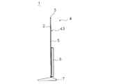
- FIG. 1 is a perspective view schematically illustrating a display device according to Embodiment 1.
- FIG. It is a side view which briefly displays a display apparatus.
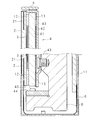
- FIG. 3 is a partial longitudinal sectional view taken along line III-III of FIG.
- FIG. 1 is a perspective view schematically illustrating the display device according to the first embodiment.
- FIG. 2 is a side view schematically illustrating the display device.
- the display device is the liquid crystal display device 1 including the liquid crystal panel 2 as a display panel for image display.
- the liquid crystal display device 1 includes a backlight 4 for irradiating the liquid crystal panel 2 with light.
- the liquid crystal panel 2 has a rectangular plate shape, and includes a display unit that displays an image on the front.
- the back side of the liquid crystal panel 2 is covered by a backlight chassis 43 (storage container) which constitutes an outer casing of the backlight 4.
- the backlight chassis 43 constitutes an exterior body of the liquid crystal display device 1.
- the liquid crystal display device 1 shown in FIG. 1 is configured as a television receiver including a receiving unit 9 and a signal processing unit 10.
- the receiving unit 9 is connected to an antenna (not shown) and receives television broadcast through the antenna.
- the signal processing unit 10 demodulates the data related to the television broadcast received by the receiving unit 9, separates the image data from the demodulated data, and outputs the separated image data.
- the liquid crystal panel 2 displays an image based on the image data output from the signal processing unit 10.
- the liquid crystal display device 1 includes the legs 7.
- the liquid crystal display device 1 is supported by the legs 7 and placed on a flat table, and is used while keeping the display surface of the liquid crystal panel 2 in the vertical posture.
- the display surface side of the liquid crystal panel 2 is referred to as the front, and the other surface is referred to as the rear.
- upper and lower correspond to upper and lower in the above-mentioned use state
- left and right correspond to left and right as viewed from the front side in use.
- FIG. 3 is a partial longitudinal sectional view taken along line III-III of FIG. In this partial longitudinal sectional view, parts of the upper and lower portions of the liquid crystal display device 1 are shown.
- the backlight 4 includes a light guide plate 41 inside the backlight chassis 43.
- the back light chassis 43 is a metal case formed in a shallow bottom dish shape by raising the peripheral edge of a rectangular bottom plate substantially vertically to surround short side walls.
- the light guide plate 41 is a flat plate made of glass or a translucent resin such as an acrylic resin, and is formed in a rectangular shape.
- the light guide plate 41 and the liquid crystal panel 2 are made of materials having substantially the same coefficient of thermal expansion.
- the light guide plate 41 is an optical member in which a reflective sheet is attached to the rear surface (rear surface) of the flat plate, and the reflective sheet 42 is attached to the remaining portion of the light guide plate 41 excluding the peripheral portion.
- the light guide plate 41 is accommodated in the backlight chassis 43 so that the adhesion surface (rear surface) of the reflection sheet 42 faces the side of the bottom plate of the backlight chassis 43 and covers substantially the entire surface of the bottom plate.
- the adhesive layer 13 is provided between the peripheral portion of the light guide plate 41 and the backlight chassis 43, and the light guide plate 41 and the backlight chassis 43 are adhered and fixed by the adhesive layer 13.
- the adhesive layer 13 is, for example, a long strip-shaped double-sided tape.
- the adhesive layer 13 is provided on the entire periphery of the peripheral portion of the surface of the light guide plate 41 on which the reflective sheet 42 is attached, that is, the upper and lower edges and the left and right edges.
- the adhesive layer 13 is not limited to a double-sided tape, but may be formed by applying an adhesive in a long strip shape to form a thickness, and bonding the light guide plate 41 and the backlight chassis 43.
- the light guide plate 41 has a front surface (front surface) facing the liquid crystal panel 2, and the light guide plate 41 and the liquid crystal panel 2 are bonded by an adhesive member 12 provided on the peripheral edge of the facing surface.
- the bonding member 12 is, for example, a long strip-shaped double-sided tape in which the bonding layer 13 is provided on both sides of a thick base material.
- the bonding members 12 are provided all around the periphery of the facing surface, that is, the upper and lower edges and the left and right edges.
- the bonding member 12 is provided in a region corresponding to the black matrix 21 of the liquid crystal panel 2 described later.
- a gap corresponding to the thickness of the bonding member 12 is formed between the light guide plate 41 and the liquid crystal panel 2, and the optical sheet group 3 is interposed in the gap.
- the size of the gap is preferably larger than the thickness of the optical sheet group 3 in the range of 0.2 mm to 0.6 mm. Furthermore, it is desirable to set the distance between the optical sheet group 3 and the liquid crystal panel 2 to about 0.4 mm.
- the bonding member 12 is not limited to the double-sided tape, but may be a thick strip by applying a bonding agent to form a thickness, and bonding the light guide plate 41 and the liquid crystal panel 2.
- the backlight 4 includes an LED 45 and a light source substrate 44 on which the LED 45 is mounted.
- the light source substrate 44 is fixed to the heat spreader 8 screwed to the lower portion on the back side of the backlight chassis 43, and the mounting surface of the LED 45 is provided to face the lower edge of the light guide plate 41.
- the light source substrate 44 is in the form of a long strip having a length corresponding to the lower edge of the light guide plate 41, and the LEDs 45 are mounted side by side in the longitudinal direction of the light source substrate 441.
- the heat generated by the lighting of the LED 45 is dissipated through the heat spreader 8 and the back light chassis 43.
- the liquid crystal panel 2 has a known configuration in which liquid crystal is sealed between an array substrate and a color filter substrate, and polarizing plates are laminated on both sides of these.
- the liquid crystal panel 2 is made of glass or a transparent resin such as an acrylic resin.
- a black matrix 21 for forming an area through which light for displaying an image is not transmitted is provided in the peripheral portion of the liquid crystal panel 2.
- the liquid crystal sealed between the array substrate and the color filter substrate is driven by the liquid crystal drive substrate 11 connected to the liquid crystal panel 2 via a lead.
- a side plate 5 is provided to face the outer surface of the side wall of the back light chassis 43.
- the side plate 5 has a rectangular plate shape, is made of resin or metal, and forms an outer shell of the side surface of the liquid crystal display device 1.
- the side plates 5 are provided on the upper portion and the left and right side walls of the backlight chassis 43.
- the length in the longitudinal direction of the side plate 5 is set to be substantially the same as the length of the side wall of the corresponding backlight chassis 43.
- the backlight chassis 43 and the side plate 5 are adhered and fixed by a double-sided tape or an adhesive provided between the outer surface of the side wall of the backlight chassis 43 and the inner surface of the side plate 5.
- the side plate 5 is made of resin, the backlight chassis 43 and the side plate 5 may be welded and fixed.
- the liquid crystal display device 1 includes a box-shaped cover 6.
- the cover 6 is disposed on the lower side of the liquid crystal display panel, and is provided to cover the backlight chassis 43 from the rear side.
- the light emitted from the LED 45 is incident on the light guide plate 41 through the lower edge facing the light source substrate 44, and is totally reflected by the reflection sheet attached to the rear surface (other surface) inside the light guide plate 41 and the front surface (one surface). The partial reflection is repeated and proceeds to be distributed over the entire front surface of the light guide plate 41 and emitted.
- the emitted light is diffused by the optical sheet group 3 and irradiated to the back surface of the liquid crystal panel 2, and the liquid crystal panel 2 modulates and transmits the emitted light from the backlight 4 by driving of the liquid crystal sealed therein. Display the image on the front.
- the light guide plate 41 and the liquid crystal panel 2 are bonded by the adhesive member 12 provided on the peripheral portion between the facing surfaces, the light guide plate 41 and the liquid crystal panel 2 can be fixed with a simple configuration.
- the thickness of the bonding member 12 is set so that the gap between the facing surfaces of the light guide plate 41 and the liquid crystal panel 2 is larger than the thickness of the optical sheet group 3 in the range of 0.2 mm to 0.6 mm. Is desirable.
- the thickness of the bonding member 12 is set by setting the thickness of the bonding member 12 so that the gap between the facing surfaces of the light guide plate 41 and the liquid crystal panel 2 is larger than the thickness of the optical sheet group 3 in the range of 0.2 mm to 0.6 mm. An appropriate distance between the optical sheet group 3 and the liquid crystal panel 2 can be secured while reducing the thickness of the display device 1.
- the light guide plate 41 and the liquid crystal panel 2 thermally expand and expand in the respective thickness directions, a sufficient distance between the light guide plate 41 and the liquid crystal panel 2 can be secured.
- an appropriate distance by setting the distance between the optical sheet group 3 and the liquid crystal panel 2 to, for example, 0.4 mm, an image can be clearly displayed on the display unit of the liquid crystal display panel.
- the gap between the facing surfaces of the light guide plate 41 and the liquid crystal panel 2 may be 0.1 mm to 2 mm. By setting the gap to 2 mm or less, the tolerance to the change of the optical sheet group 3 can be increased. Further, by setting the gap to 0.1 mm or more, the load on the optical sheet group 3 can be reduced while the optical sheet group 3 and the liquid crystal panel 2 are substantially in close contact with each other. Thinning can be further promoted.
- the bonding members 12 are provided in the region of the black matrix 21 of the liquid crystal panel 2, it is possible to avoid affecting the image displayed on the display unit of the liquid crystal panel 2.
- the light guide plate 41 and the liquid crystal panel 2 are made of materials having substantially the same coefficient of thermal expansion. Even if the light guide plate 41 and the liquid crystal panel 2 thermally expand due to the heat generated with the light emission of the LED 45, the shear stress generated in the adhesive member 12 can be reduced, and the adhesive function of the adhesive member 12 can be secured.
- the thermal expansion coefficient is substantially the same, when a shear stress is generated in the bonding member 12 due to the difference between the respective thermal expansion coefficients, the thermal expansion coefficient of each bonding member 12 is not impaired by the shearing stress. Means that the difference between Therefore, materials made of materials having substantially the same coefficient of thermal expansion are not limited to the case where the light guide plate 41 and the liquid crystal panel 2 are made of the same material such as glass or acrylic resin, etc. Also, the thermal expansion coefficients may be substantially the same.
- the back light chassis 43 and the light guide plate 41 are bonded by the adhesive layer 13 provided on the peripheral portion between the facing surfaces, it is possible to fix the light guide plate 41 and the back light chassis 43 with a simple configuration. it can.
- fixing the light guide plate 41 to the liquid crystal panel 2 and the backlight chassis 43 it is possible to suppress the occurrence of positional deviation among the light guide plate 41, the liquid crystal panel 2 and the backlight chassis 43.
- the back light chassis 43 of iron and making the light guide plate 41 of glass the difference in thermal expansion coefficient between the back light chassis 43 and the light guide plate 41 can be reduced.
- the difference in thermal expansion coefficient between the backlight chassis 43 and the light guide plate 41 By reducing the difference in thermal expansion coefficient between the backlight chassis 43 and the light guide plate 41, when the backlight chassis 43 and the light guide plate 41 thermally expand, the shear stress generated in the adhesive layer 13 is reduced, and the adhesive layer 13 adhesive functions can be secured. Further, by reducing the difference in thermal expansion coefficient between the backlight chassis 43 and the light guide plate 41, the distance between the inner surface of the side wall of the backlight chassis 43 and the side surface of the light guide plate 41 facing the inner surface is reduced. It is possible to reduce the amount of money. Further, for example, by making the back light chassis 43 of iron and making the liquid crystal display panel of glass, the difference in thermal expansion coefficient between the back light chassis 43 and the liquid crystal display panel can be reduced.
- the inner surface of the side plate 5 bonded to the side wall of the backlight chassis 43 and the side surface of the liquid crystal panel 2 facing the inner surface It is possible to reduce the distance by reducing the distance.
- the appearance of the liquid crystal display device 1 can be improved.
- the side plate 5 and the back light chassis 43 are bonded by a double-sided tape or an adhesive provided between the outer surface of the side wall of the back light chassis 43 and the inner surface of the side plate 5. And the side plate 5 can be fixed.
- a display panel 2 for displaying an image on the front and a back surface of the display panel 2 are disposed opposite to each other, and light emitted from the one surface is the display panel
- the display panel 2 and the light guide plate 41 separate the gap between the opposing surfaces by the adhesion of the respective peripheral portions. It is characterized in that it is fixed.
- the display panel 2 and the light guide plate 41 can be fixed with a simple configuration by bonding at the periphery of the facing surface of the display panel 2 and the light guide plate 41.
- the display device 1 is characterized in that the display panel 2 and the light guide plate 41 are made of materials having substantially the same coefficient of thermal expansion.
- the display panel 2 and the light guide plate 41 made of materials having substantially the same coefficient of thermal expansion, excessive shear stress is generated at the bonded portion even if the display panel 2 and the light guide plate 41 thermally expand. Can be suppressed, and secure fixing of the display panel 2 and the light guide plate 41 can be secured.
- the display device 1 is characterized in that the width of the gap is larger than the thickness of the optical sheet 3 in a range of 0.2 mm or more and 0.6 mm or less.
- the width of the gap between the facing surfaces where the display panel 2 and the light guide plate 41 are bonded is thicker than the thickness of the optical sheet 3 in the range of 0.1 mm or more and 2 mm or less . Therefore, an appropriate distance can be secured between the optical sheet 3 and the display panel 2, and an image can be clearly displayed on the display unit of the liquid crystal panel.
- the display device 1 according to the embodiment of the present disclosure is characterized in that the width of the gap is 0.1 mm or more and 2 mm or less.
- the width of the gap between the facing surfaces where the display panel 2 and the light guide plate 41 are bonded is set in the range of 0.1 mm or more and 2 mm or less. Therefore, the tolerance to the change of the optical sheet 3 can be increased, and while the optical sheet 3 and the display panel 2 are in close contact with each other, the load on the optical sheet 3 is reduced, and the display device 1 is thinned. Can proceed.
- the display device 1 is characterized in that the light guide plate 41 and the display panel 2 are bonded in a region of the black matrix 21 of the display panel 2.
- the portion of the display panel 2 bonded to the light guide plate 41 is in the area of the black matrix 21 of the display panel 2, and thus the image on the display portion of the display panel 2 is affected. It can be avoided.
- the display device 1 includes a plate-shaped storage container 43 that stores the light guide plate 41 so as to cover the other surface side, and the storage container 43 and the light guide plate 41 have opposing surfaces. It is characterized in that it is bonded at the periphery.
- the light guide plate 41 stored in the storage container 43 can be fixed with a simple configuration.
- the occurrence of positional deviation between the light guide plate 41, the display panel 2 and the storage container 43 can be suppressed.
- the display device 1 is characterized by including a side plate 5 fixed to the outer side surface of the storage container 43.
- the appearance of the display device 1 can be improved.
- a display device 1 according to an embodiment of the present disclosure includes the display device 1 according to an embodiment of the present disclosure, and a receiving unit 9 that receives a television broadcast, and based on the television broadcast received by the receiving unit 9 An image is displayed on the display panel 2.
- the present embodiment by using the above-described display device 1, it is possible to provide a television receiver in which the display panel 2 and the light guide plate 41 are fixed with a simple configuration.
Landscapes
- Physics & Mathematics (AREA)
- Nonlinear Science (AREA)
- Liquid Crystal (AREA)
- Mathematical Physics (AREA)
- Chemical & Material Sciences (AREA)
- Crystallography & Structural Chemistry (AREA)
- General Physics & Mathematics (AREA)
- Optics & Photonics (AREA)
- Planar Illumination Modules (AREA)
Abstract
L'invention concerne un dispositif d'affichage permettant, à l'aide d'une structure simple, de fixer une plaque de guidage de lumière et un panneau d'affichage. Plus spécifiquement, ce dispositif d'affichage comporte: un panneau d'affichage (2) pour afficher une image sur la surface avant du dispositif; ainsi qu'une plaque (41) de guidage de lumière, laquelle est située de façon qu'une face soit opposée à la face arrière du panneau d'affichage (2), et laquelle fait en sorte qu'une lumière sortant de la face susmentionnée éclaire la surface arrière du panneau d'affichage (2). Les bords de circonférence du panneau d'affichage (2) et de la plaque (41) de guidage de lumière sont joints et fixés, une feuille optique (3) étant située entre les deux.
Applications Claiming Priority (2)
| Application Number | Priority Date | Filing Date | Title |
|---|---|---|---|
| JP2017183857A JP6531146B2 (ja) | 2017-09-25 | 2017-09-25 | 表示装置及びテレビジョン受信機 |
| JP2017-183857 | 2017-09-25 |
Publications (1)
| Publication Number | Publication Date |
|---|---|
| WO2019059353A1 true WO2019059353A1 (fr) | 2019-03-28 |
Family
ID=65809891
Family Applications (1)
| Application Number | Title | Priority Date | Filing Date |
|---|---|---|---|
| PCT/JP2018/035068 Ceased WO2019059353A1 (fr) | 2017-09-25 | 2018-09-21 | Dispositif d'affichage et récepteur de télévision |
Country Status (2)
| Country | Link |
|---|---|
| JP (1) | JP6531146B2 (fr) |
| WO (1) | WO2019059353A1 (fr) |
Cited By (1)
| Publication number | Priority date | Publication date | Assignee | Title |
|---|---|---|---|---|
| CN112859448A (zh) * | 2021-03-17 | 2021-05-28 | 重庆京东方显示照明有限公司 | 胶带、背光模组、显示装置和背光模组的制备方法 |
Families Citing this family (2)
| Publication number | Priority date | Publication date | Assignee | Title |
|---|---|---|---|---|
| WO2019230515A1 (fr) * | 2018-05-31 | 2019-12-05 | パナソニックIpマネジメント株式会社 | Dispositif d'affichage d'images |
| JP6889816B1 (ja) * | 2019-08-23 | 2021-06-18 | ミネベアミツミ株式会社 | 面状照明装置 |
Citations (4)
| Publication number | Priority date | Publication date | Assignee | Title |
|---|---|---|---|---|
| US20140176867A1 (en) * | 2012-11-14 | 2014-06-26 | Shenzhen China Star Optoelectronics Technology Co, Ltd. | Edge type backlight module and liquid crystal display for preventing light leakage |
| US20150355506A1 (en) * | 2014-06-09 | 2015-12-10 | Samsung Display Co., Ltd. | Liquid crystal display |
| WO2016139718A1 (fr) * | 2015-03-02 | 2016-09-09 | 堺ディスプレイプロダクト株式会社 | Dispositif d'affichage et procédé de fabrication de dispositif d'affichage |
| CN206209230U (zh) * | 2016-10-12 | 2017-05-31 | 合肥惠科金扬科技有限公司 | 无边框显示器防漏光结构及无边框显示器 |
-
2017
- 2017-09-25 JP JP2017183857A patent/JP6531146B2/ja active Active
-
2018
- 2018-09-21 WO PCT/JP2018/035068 patent/WO2019059353A1/fr not_active Ceased
Patent Citations (4)
| Publication number | Priority date | Publication date | Assignee | Title |
|---|---|---|---|---|
| US20140176867A1 (en) * | 2012-11-14 | 2014-06-26 | Shenzhen China Star Optoelectronics Technology Co, Ltd. | Edge type backlight module and liquid crystal display for preventing light leakage |
| US20150355506A1 (en) * | 2014-06-09 | 2015-12-10 | Samsung Display Co., Ltd. | Liquid crystal display |
| WO2016139718A1 (fr) * | 2015-03-02 | 2016-09-09 | 堺ディスプレイプロダクト株式会社 | Dispositif d'affichage et procédé de fabrication de dispositif d'affichage |
| CN206209230U (zh) * | 2016-10-12 | 2017-05-31 | 合肥惠科金扬科技有限公司 | 无边框显示器防漏光结构及无边框显示器 |
Cited By (3)
| Publication number | Priority date | Publication date | Assignee | Title |
|---|---|---|---|---|
| CN112859448A (zh) * | 2021-03-17 | 2021-05-28 | 重庆京东方显示照明有限公司 | 胶带、背光模组、显示装置和背光模组的制备方法 |
| CN112859448B (zh) * | 2021-03-17 | 2023-03-14 | 重庆京东方显示照明有限公司 | 胶带、背光模组、显示装置和背光模组的制备方法 |
| US11709311B2 (en) | 2021-03-17 | 2023-07-25 | Chongqing Boe Display Lighting Co., Ltd. | Adhesive tape, backlight module, display device and method for manufacturing backlight module |
Also Published As
| Publication number | Publication date |
|---|---|
| JP6531146B2 (ja) | 2019-06-12 |
| JP2019060969A (ja) | 2019-04-18 |
Similar Documents
| Publication | Publication Date | Title |
|---|---|---|
| US10371887B2 (en) | Display apparatus with U-shaped coupling member | |
| KR20070042909A (ko) | 백라이트 장치 | |
| US20140036197A1 (en) | Liquid Crystal Module and Liquid Crystal Display Device | |
| US20120162566A1 (en) | Television and electronic apparatus | |
| CN102022673A (zh) | 背光单元和具有该背光单元的液晶显示设备 | |
| KR101994014B1 (ko) | 액정 패널 및 백라이트 모듈 위치설정 접착 구조체와 디스플레이 장치 | |
| US9897747B2 (en) | Display apparatus | |
| EP3226070B1 (fr) | Module à cristaux liquides et dispositif d'affichage | |
| US9952458B2 (en) | Display apparatus | |
| JP2004119369A (ja) | バックライトアセンブリ及びこれを利用した液晶表示装置 | |
| TWI391740B (zh) | 液晶顯示裝置及液晶顯示裝置之防塵方法及液晶顯示裝置之製造方法 | |
| JP6531146B2 (ja) | 表示装置及びテレビジョン受信機 | |
| WO2016170620A1 (fr) | Dispositif de source lumineuse et dispositif d'affichage | |
| CN103713404B (zh) | 液晶显示装置及其装配方法 | |
| CN100487536C (zh) | 液晶显示装置 | |
| WO2013099765A1 (fr) | Dispositif d'affichage et élément de cadre | |
| JP2016045362A (ja) | 表示装置 | |
| US20150022759A1 (en) | Display with Radioluminescent Backlight Unit | |
| US9651824B2 (en) | Image display apparatus | |
| CN212781605U (zh) | 背光模组及液晶显示装置 | |
| JP2019060968A (ja) | 表示装置及びテレビジョン受信機 | |
| US10718896B2 (en) | Display device and television receiver | |
| JP7084741B2 (ja) | 表示装置、テレビジョン受信機及び表示装置の製造方法 | |
| CN111694186A (zh) | 显示装置 | |
| KR102009799B1 (ko) | 백 라이트 유닛과 이를 이용한 액정 표시장치 |
Legal Events
| Date | Code | Title | Description |
|---|---|---|---|
| 121 | Ep: the epo has been informed by wipo that ep was designated in this application |
Ref document number: 18858959 Country of ref document: EP Kind code of ref document: A1 |
|
| NENP | Non-entry into the national phase |
Ref country code: DE |
|
| 122 | Ep: pct application non-entry in european phase |
Ref document number: 18858959 Country of ref document: EP Kind code of ref document: A1 |