WO2016139718A1 - Dispositif d'affichage et procédé de fabrication de dispositif d'affichage - Google Patents
Dispositif d'affichage et procédé de fabrication de dispositif d'affichage Download PDFInfo
- Publication number
- WO2016139718A1 WO2016139718A1 PCT/JP2015/056080 JP2015056080W WO2016139718A1 WO 2016139718 A1 WO2016139718 A1 WO 2016139718A1 JP 2015056080 W JP2015056080 W JP 2015056080W WO 2016139718 A1 WO2016139718 A1 WO 2016139718A1
- Authority
- WO
- WIPO (PCT)
- Prior art keywords
- display device
- thickness
- guide plate
- light guide
- space holding
- Prior art date
- Legal status (The legal status is an assumption and is not a legal conclusion. Google has not performed a legal analysis and makes no representation as to the accuracy of the status listed.)
- Ceased
Links
Images


Classifications
-
- G—PHYSICS
- G02—OPTICS
- G02B—OPTICAL ELEMENTS, SYSTEMS OR APPARATUS
- G02B6/00—Light guides; Structural details of arrangements comprising light guides and other optical elements, e.g. couplings
- G02B6/0001—Light guides; Structural details of arrangements comprising light guides and other optical elements, e.g. couplings specially adapted for lighting devices or systems
- G02B6/0011—Light guides; Structural details of arrangements comprising light guides and other optical elements, e.g. couplings specially adapted for lighting devices or systems the light guides being planar or of plate-like form
- G02B6/0081—Mechanical or electrical aspects of the light guide and light source in the lighting device peculiar to the adaptation to planar light guides, e.g. concerning packaging
- G02B6/0086—Positioning aspects
- G02B6/0088—Positioning aspects of the light guide or other optical sheets in the package
-
- B—PERFORMING OPERATIONS; TRANSPORTING
- B32—LAYERED PRODUCTS
- B32B—LAYERED PRODUCTS, i.e. PRODUCTS BUILT-UP OF STRATA OF FLAT OR NON-FLAT, e.g. CELLULAR OR HONEYCOMB, FORM
- B32B37/00—Methods or apparatus for laminating, e.g. by curing or by ultrasonic bonding
- B32B37/02—Methods or apparatus for laminating, e.g. by curing or by ultrasonic bonding characterised by a sequence of laminating steps, e.g. by adding new layers at consecutive laminating stations
-
- G—PHYSICS
- G02—OPTICS
- G02B—OPTICAL ELEMENTS, SYSTEMS OR APPARATUS
- G02B6/00—Light guides; Structural details of arrangements comprising light guides and other optical elements, e.g. couplings
- G02B6/0001—Light guides; Structural details of arrangements comprising light guides and other optical elements, e.g. couplings specially adapted for lighting devices or systems
- G02B6/0011—Light guides; Structural details of arrangements comprising light guides and other optical elements, e.g. couplings specially adapted for lighting devices or systems the light guides being planar or of plate-like form
- G02B6/0033—Means for improving the coupling-out of light from the light guide
- G02B6/005—Means for improving the coupling-out of light from the light guide provided by one optical element, or plurality thereof, placed on the light output side of the light guide
-
- G—PHYSICS
- G02—OPTICS
- G02B—OPTICAL ELEMENTS, SYSTEMS OR APPARATUS
- G02B6/00—Light guides; Structural details of arrangements comprising light guides and other optical elements, e.g. couplings
- G02B6/0001—Light guides; Structural details of arrangements comprising light guides and other optical elements, e.g. couplings specially adapted for lighting devices or systems
- G02B6/0011—Light guides; Structural details of arrangements comprising light guides and other optical elements, e.g. couplings specially adapted for lighting devices or systems the light guides being planar or of plate-like form
- G02B6/0033—Means for improving the coupling-out of light from the light guide
- G02B6/005—Means for improving the coupling-out of light from the light guide provided by one optical element, or plurality thereof, placed on the light output side of the light guide
- G02B6/0051—Diffusing sheet or layer
-
- G—PHYSICS
- G02—OPTICS
- G02B—OPTICAL ELEMENTS, SYSTEMS OR APPARATUS
- G02B6/00—Light guides; Structural details of arrangements comprising light guides and other optical elements, e.g. couplings
- G02B6/0001—Light guides; Structural details of arrangements comprising light guides and other optical elements, e.g. couplings specially adapted for lighting devices or systems
- G02B6/0011—Light guides; Structural details of arrangements comprising light guides and other optical elements, e.g. couplings specially adapted for lighting devices or systems the light guides being planar or of plate-like form
- G02B6/0065—Manufacturing aspects; Material aspects
-
- B—PERFORMING OPERATIONS; TRANSPORTING
- B32—LAYERED PRODUCTS
- B32B—LAYERED PRODUCTS, i.e. PRODUCTS BUILT-UP OF STRATA OF FLAT OR NON-FLAT, e.g. CELLULAR OR HONEYCOMB, FORM
- B32B37/00—Methods or apparatus for laminating, e.g. by curing or by ultrasonic bonding
- B32B37/14—Methods or apparatus for laminating, e.g. by curing or by ultrasonic bonding characterised by the properties of the layers
- B32B37/24—Methods or apparatus for laminating, e.g. by curing or by ultrasonic bonding characterised by the properties of the layers with at least one layer not being coherent before laminating, e.g. made up from granular material sprinkled onto a substrate
- B32B2037/243—Coating
-
- B—PERFORMING OPERATIONS; TRANSPORTING
- B32—LAYERED PRODUCTS
- B32B—LAYERED PRODUCTS, i.e. PRODUCTS BUILT-UP OF STRATA OF FLAT OR NON-FLAT, e.g. CELLULAR OR HONEYCOMB, FORM
- B32B2310/00—Treatment by energy or chemical effects
- B32B2310/08—Treatment by energy or chemical effects by wave energy or particle radiation
- B32B2310/0806—Treatment by energy or chemical effects by wave energy or particle radiation using electromagnetic radiation
- B32B2310/0831—Treatment by energy or chemical effects by wave energy or particle radiation using electromagnetic radiation using UV radiation
-
- B—PERFORMING OPERATIONS; TRANSPORTING
- B32—LAYERED PRODUCTS
- B32B—LAYERED PRODUCTS, i.e. PRODUCTS BUILT-UP OF STRATA OF FLAT OR NON-FLAT, e.g. CELLULAR OR HONEYCOMB, FORM
- B32B2457/00—Electrical equipment
- B32B2457/20—Displays, e.g. liquid crystal displays, plasma displays
- B32B2457/202—LCD, i.e. liquid crystal displays
-
- B—PERFORMING OPERATIONS; TRANSPORTING
- B32—LAYERED PRODUCTS
- B32B—LAYERED PRODUCTS, i.e. PRODUCTS BUILT-UP OF STRATA OF FLAT OR NON-FLAT, e.g. CELLULAR OR HONEYCOMB, FORM
- B32B37/00—Methods or apparatus for laminating, e.g. by curing or by ultrasonic bonding
- B32B37/14—Methods or apparatus for laminating, e.g. by curing or by ultrasonic bonding characterised by the properties of the layers
- B32B37/24—Methods or apparatus for laminating, e.g. by curing or by ultrasonic bonding characterised by the properties of the layers with at least one layer not being coherent before laminating, e.g. made up from granular material sprinkled onto a substrate
-
- G—PHYSICS
- G02—OPTICS
- G02F—OPTICAL DEVICES OR ARRANGEMENTS FOR THE CONTROL OF LIGHT BY MODIFICATION OF THE OPTICAL PROPERTIES OF THE MEDIA OF THE ELEMENTS INVOLVED THEREIN; NON-LINEAR OPTICS; FREQUENCY-CHANGING OF LIGHT; OPTICAL LOGIC ELEMENTS; OPTICAL ANALOGUE/DIGITAL CONVERTERS
- G02F1/00—Devices or arrangements for the control of the intensity, colour, phase, polarisation or direction of light arriving from an independent light source, e.g. switching, gating or modulating; Non-linear optics
- G02F1/01—Devices or arrangements for the control of the intensity, colour, phase, polarisation or direction of light arriving from an independent light source, e.g. switching, gating or modulating; Non-linear optics for the control of the intensity, phase, polarisation or colour
- G02F1/13—Devices or arrangements for the control of the intensity, colour, phase, polarisation or direction of light arriving from an independent light source, e.g. switching, gating or modulating; Non-linear optics for the control of the intensity, phase, polarisation or colour based on liquid crystals, e.g. single liquid crystal display cells
- G02F1/133—Constructional arrangements; Operation of liquid crystal cells; Circuit arrangements
- G02F1/1333—Constructional arrangements; Manufacturing methods
- G02F1/133308—Support structures for LCD panels, e.g. frames or bezels
-
- G—PHYSICS
- G02—OPTICS
- G02F—OPTICAL DEVICES OR ARRANGEMENTS FOR THE CONTROL OF LIGHT BY MODIFICATION OF THE OPTICAL PROPERTIES OF THE MEDIA OF THE ELEMENTS INVOLVED THEREIN; NON-LINEAR OPTICS; FREQUENCY-CHANGING OF LIGHT; OPTICAL LOGIC ELEMENTS; OPTICAL ANALOGUE/DIGITAL CONVERTERS
- G02F1/00—Devices or arrangements for the control of the intensity, colour, phase, polarisation or direction of light arriving from an independent light source, e.g. switching, gating or modulating; Non-linear optics
- G02F1/01—Devices or arrangements for the control of the intensity, colour, phase, polarisation or direction of light arriving from an independent light source, e.g. switching, gating or modulating; Non-linear optics for the control of the intensity, phase, polarisation or colour
- G02F1/13—Devices or arrangements for the control of the intensity, colour, phase, polarisation or direction of light arriving from an independent light source, e.g. switching, gating or modulating; Non-linear optics for the control of the intensity, phase, polarisation or colour based on liquid crystals, e.g. single liquid crystal display cells
- G02F1/133—Constructional arrangements; Operation of liquid crystal cells; Circuit arrangements
- G02F1/1333—Constructional arrangements; Manufacturing methods
- G02F1/133308—Support structures for LCD panels, e.g. frames or bezels
- G02F1/133317—Intermediate frames, e.g. between backlight housing and front frame
-
- G—PHYSICS
- G02—OPTICS
- G02F—OPTICAL DEVICES OR ARRANGEMENTS FOR THE CONTROL OF LIGHT BY MODIFICATION OF THE OPTICAL PROPERTIES OF THE MEDIA OF THE ELEMENTS INVOLVED THEREIN; NON-LINEAR OPTICS; FREQUENCY-CHANGING OF LIGHT; OPTICAL LOGIC ELEMENTS; OPTICAL ANALOGUE/DIGITAL CONVERTERS
- G02F1/00—Devices or arrangements for the control of the intensity, colour, phase, polarisation or direction of light arriving from an independent light source, e.g. switching, gating or modulating; Non-linear optics
- G02F1/01—Devices or arrangements for the control of the intensity, colour, phase, polarisation or direction of light arriving from an independent light source, e.g. switching, gating or modulating; Non-linear optics for the control of the intensity, phase, polarisation or colour
- G02F1/13—Devices or arrangements for the control of the intensity, colour, phase, polarisation or direction of light arriving from an independent light source, e.g. switching, gating or modulating; Non-linear optics for the control of the intensity, phase, polarisation or colour based on liquid crystals, e.g. single liquid crystal display cells
- G02F1/133—Constructional arrangements; Operation of liquid crystal cells; Circuit arrangements
- G02F1/1333—Constructional arrangements; Manufacturing methods
- G02F1/1335—Structural association of cells with optical devices, e.g. polarisers or reflectors
- G02F1/1336—Illuminating devices
- G02F1/133615—Edge-illuminating devices, i.e. illuminating from the side
Definitions
- the present invention relates to a display device and a method for manufacturing the display device.
- a display device including a liquid crystal panel as an image display unit includes a backlight on the back side of the liquid crystal panel, modulates and transmits the light emitted from the backlight by the liquid crystal panel, and displays an image on the front of the liquid crystal panel. It is configured as follows. Backlights are roughly classified into direct type and edge light type. In recent years, edge light type backlights are widely used from the viewpoint of reducing power consumption and reducing the thickness.
- Edge light type backlight includes a light guide plate and a light source housed in a backlight chassis having a shallow box shape.
- the light guide plate is a flat plate made of glass or a resin material having translucency, and is placed on the bottom plate of the backlight chassis.
- the light source is attached to one side wall of the backlight chassis and is opposed to one side surface of the light guide plate. Light emitted from the light source is incident on one side of the light guide plate, travels through the light guide plate, and is distributed and emitted over the entire wide surface of the light guide plate exposed to the opening side of the backlight chassis.
- the display device is configured such that a wide surface of the light guide plate is opposed to the back surface of the liquid crystal panel, and an optical sheet is interposed between the opposed surfaces.
- the optical sheet is an optical element that functions to diffuse and collect light, and light emitted from the light guide plate is irradiated onto the liquid crystal panel through the optical sheet.
- a display device has been proposed in which a spacer is provided between the light guide plate and the liquid crystal panel and a space for interposing the optical sheet is secured.
- the display device (display module) described in Patent Document 1 the light guide plate and the liquid crystal panel are opposed to each other with an appropriate interval by a frame-like spacer provided on each peripheral portion, and an optical sheet Is disposed in the inner space of the spacer.
- an optical sheet is disposed on a wide surface of a light guide plate, and a spacer is temporarily fixed on the light guide plate using a double-sided adhesive sheet so as to surround the optical sheet. Thereafter, an adhesive is applied to the outer periphery of the spacer, the display panel is placed on the spacer, the adhesive is heated or irradiated with UV to solidify the adhesive, and the light guide plate and the liquid crystal panel are combined.
- the present invention has been made in view of such circumstances, and an object of the present invention is to provide a display device and a display device manufacturing method capable of accurately positioning an optical sheet.
- a display device includes a display panel for displaying an image on one surface, a light guide plate disposed opposite to the other surface of the display panel, and a plurality of optical sheets interposed between the display panel and the light guide plate. And a spacer that is sandwiched between the display panel and the light guide plate and secures a space for interposing the optical sheet, wherein the spacer is fixed to the light guide plate to secure the space.
- a holding layer, and a fixing layer sandwiched between the display panel and the space holding layer and fixed to the display panel, and the thickness of the space holding layer is the plurality of except for the optical sheet closest to the display panel It is characterized by being thicker than the total thickness of one optical sheet.
- the spacer is separated into the space holding layer and the fixing layer, and the thickness of the space holding layer is larger than the total thickness of the plurality of optical sheets excluding the optical sheet closest to the display panel. It is thick.
- the optical sheet can be accurately positioned. Moreover, the increase in the thickness of the display device due to the spacer can be suppressed by setting the thickness of the space holding layer to the minimum thickness that restricts the movement of the optical sheet.
- the fixing layer can be made thin. Therefore, the thickness of the spacer can be brought close to the thickness of the space retaining layer, and the error between the actual thickness of the spacer and the specified thickness can be reduced during manufacturing to be less than the maximum allowable dimension. Dimensional accuracy can be improved.
- the display device is characterized in that a thickness of the space holding layer is thicker than a total thickness of the plurality of optical sheets.
- the optical sheet when the display device is manufactured, the optical sheet is reliably locked to the space holding layer and the movement is restricted, so that the optical sheet can be positioned more accurately. Further, since the spacer has a thickness secured by the space holding layer, the fixing layer can be made thin. Therefore, the thickness of the spacer can be brought close to the thickness of the space retaining layer, and the error between the actual thickness of the spacer and the specified thickness can be reduced during manufacturing to be less than the maximum allowable dimension. Dimensional accuracy can be improved.
- the display device according to the present invention is characterized in that a thickness of the fixing layer is thinner than a thickness of the space holding layer.
- the thickness of the spacer can be made closer to the thickness of the space holding layer by making the thickness of the fixing layer thinner than the thickness of the space holding layer.
- the display device according to the present invention is characterized in that the fixed layer is formed of a material that starts curing after 1 to 5 minutes from UV irradiation.
- the material of the fixing layer is irradiated with UV
- curing starts at least one minute later. Therefore, when the display panel is placed on the material before the material is solidified, a sufficient time can be secured for the work.
- the curing starts 5 minutes after the UV irradiation at the latest, the display device can be manufactured efficiently.
- the display device manufacturing method is the above-described display device manufacturing method, in which the space holding layer is formed by painting and solidifying a solidifying liquid, and after the forming step, an optical sheet is formed.
- a laminating step of laminating the coating, a coating step of coating a solidifying liquid on the space holding layer after the laminating step, and placing the display panel on the liquid before solidifying the coated liquid And a mounting step.
- the optical sheet is laminated after the space holding layer is formed. Therefore, since an optical sheet is latched by a space holding layer and a movement is controlled, positioning can be performed correctly.
- the optical sheet is laminated on the light guide plate after the space holding layer is formed by solidifying the liquid, the optical sheet is not fixed unintentionally by contacting the liquid that is not solidified.
- the method for manufacturing a display device includes a pressing step of pressing the liquid crystal panel from the one surface side after the placing step and before the liquid is solidified.
- the fixing strength of the fixing layer can be increased.
- the fixing layer can be extended thinly, and the thickness of the spacer can be brought close to the thickness of the space holding layer. Thereby, at the time of manufacture, the error between the actual thickness of the spacer and the specified thickness can be reduced to the maximum allowable dimension or less, and the dimensional accuracy of the spacer can be increased.
- the method for manufacturing a display device according to the present invention is characterized in that the liquid is a UV curable resin.
- the liquid can be easily solidified by UV irradiation.
- the method for manufacturing a display device according to the present invention is characterized in that the liquid coated on the space holding layer in the coating step is a material that starts curing 1 to 5 minutes after UV irradiation.
- the liquid coated on the space holding layer in the painting process starts to be cured at least one minute after the UV irradiation, so that the time required for the painting process and the placing process can be secured. Further, since the liquid starts to be cured at least 5 minutes after the UV irradiation, the display device can be manufactured efficiently.
- the optical sheet can be accurately positioned.
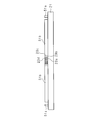
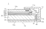
- FIG. 3 is a cross-sectional view showing a main part of the display device according to Embodiment 1.
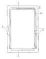
- FIG. FIG. 2 is a cross-sectional view taken along line II-II in FIG. It is a side view which shows the structure of a spacer.
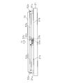
- FIG. 6 is a cross-sectional view showing a main part of a display device according to
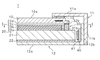
- FIG. 1 is a cross-sectional view illustrating a main part of the display device 1 according to the first embodiment.
- the display device 1 includes a liquid crystal panel 10, a bezel 11, a backlight chassis 12, and a backlight 20.
- the liquid crystal panel 10 has a rectangular shape, and the display surface 10a for displaying an image is the front.
- the backlight chassis 12 is disposed on the back side of the liquid crystal panel 10, and includes a rectangular bottom plate 12a facing the liquid crystal panel 10, and a side plate 12b rising vertically from the four sides of the bottom plate toward the liquid crystal panel 10. And has a shallow box shape with an open front side.
- the backlight 20 includes a rectangular light guide plate 21 housed in the backlight chassis 12 and a plurality of light sources 41, 41... Facing one side surface of the light guide plate 21.
- the light guide plate 21 is a flat plate made of glass or a resin material having translucency, and has one wide surface and another wide surface provided with a dot pattern for scattering light.
- the light guide plate 21 is placed on the bottom plate of the backlight chassis 12 via the reflection sheet 22.
- the other wide surface of the light guide plate 21 is in contact with the reflection sheet 22.
- the light sources 41, 41... are arranged side by side on the substrate 40 attached to one side wall of the side plate 12 b of the backlight chassis 12 corresponding to one side surface of the light guide plate 21.
- a spacer 30 is provided on one wide surface of the light guide plate 21, and the liquid crystal panel 10 is coupled to the light guide plate 21 through the spacer 30.
- the spacer 30 is fixed to the edge of the back surface of the liquid crystal panel 10 and the edge of the wide surface of the light guide plate 21.
- optical sheets 23a, 23b, 23c, and 23d that perform light diffusion and light condensing functions are disposed on one wide surface of the light guide plate 21.
- the optical sheets 23 a, 23 b, 23 c, and 23 d are arranged so as to overlap in order in the facing direction of the liquid crystal panel 10 and the light guide plate 21, and the optical sheet 23 d is arranged closest to the liquid crystal panel 10.
- Spaces for interposing the optical sheets 23a, 23b, 23c, and 23d are secured between the liquid crystal panel 10 and the light guide plate 21 by the spacer 30.
- the bezel 11 includes a rectangular frame-shaped frame 11a located on the front side of the liquid crystal panel 10, and a side plate 11b that rises vertically from the four sides forming the outer periphery of the frame toward the backlight chassis 12 side.
- the bezel 11 is placed on the liquid crystal panel 10 so that the side plate 12b contacts the side plate 12b of the backlight chassis 12.
- the peripheral edge of the display surface 10 a is covered with the frame 11 a of the bezel 11 with the cushioning material 13 interposed therebetween.
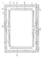
- FIG. 2 is a cross-sectional view taken along the line II-II of FIG. 1
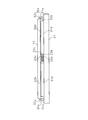
- FIG. 3 is a side view showing the structure of the spacer 30.
- Each of the optical sheets 23a, 23b, 23c, and 23d has a rectangular shape and is provided with a convex portion in a direction parallel to the surface at the center of each of the two long sides.
- the optical sheets 23 a, 23 b, 23 c, and 23 d are arranged with a convex portion on the wide surface of the light guide plate 21.
- the spacer 30 has a rectangular frame shape, is formed along the four sides of the light guide plate 21 at the edge of the wide surface of the light guide plate 21, and has two short side spacers 30 a and 30 a. And two long side spacers 30b, 30b.
- the long side spacers 30b are separated at the center in the length direction, and the opposite ends of the separated portions are bent outwardly of the light guide plate 21, respectively.
- a gap is formed in the long side spacer 30b by the opposed end portions.
- optical sheets 23 a, 23 b, 23 c, and 23 d are arranged in the inner space of the spacer 30. Moreover, each convex part of optical sheet 23a, 23b, 23c, 23d is inserted in the space
- the short side spacer 30 a is fixed to the space holding layer 31 a fixed to the light guide plate 21 and fixed to the liquid crystal panel 10 side so as to be aligned in the facing direction of the liquid crystal panel 10 and the light guide plate 21.
- Layer 32a is fixed to the space holding layer 31 a fixed to the light guide plate 21 and fixed to the liquid crystal panel 10 side so as to be aligned in the facing direction of the liquid crystal panel 10 and the light guide plate 21.
- the fixing layer 32a is thinner than the space holding layer 31a, and the fixing layer 32a and the space holding layer 31a are fixed to each other.
- the long side spacer 30b includes a space holding layer 31b and a fixing layer 32b.
- the thicknesses of the space retaining layers 31a and 31b are the same, and the thicknesses of the fixing layers 32a and 32b are the same.
- the thickness of the space holding layers 31a and 31b is thicker than the total thickness of the optical sheets 23a, 23b, 23c and 23d, and a space in which the optical sheets 23a, 23b, 23c and 23d are interposed is secured.
- the space holding layers 31a and 31b and the fixing layers 32a and 32b are preferably formed of a material that starts curing 1 to 5 minutes after UV irradiation.
- the space holding layers 31a and 31b and the fixing layers 32a and 32b are formed of a material that starts curing after 1 to 4 minutes from UV irradiation. Thereby, the display apparatus 1 can be manufactured more efficiently.
- the space holding layers 31a and 31b and the fixing layers 32a and 32b are formed of a material that starts curing after 1 to 3 minutes from UV irradiation. Thereby, the display apparatus 1 can be manufactured more efficiently.
- the optical sheets 23a, 23b, 23c, and 23d are securely locked to the space holding layers 31a and 31b, so that the movement is restricted.
- the positioning of 23b, 23c, and 23d can be performed accurately.
- the spacer 30 has a thickness secured by the space holding layers 31a and 31b, the fixing layers 32a and 32b can be made thin.
- the thickness of the spacer 30 can be made close to the thickness of the space holding layers 31a and 31b, and the error between the actual thickness of the spacer 30 and the specified thickness can be reduced to the maximum allowable dimension or less during manufacturing. Therefore, the dimensional accuracy of the spacer 30 can be increased.
- the dimensional accuracy of the spacer 30 can be similarly increased by making the thickness of the fixing layers 32a and 32b thinner than the thickness of the space holding layers 31a and 31b.
- the light emitted from the light source 41 enters from one side of the light guide plate 21, travels through the light guide plate 21, and is distributed and emitted over the entire wide surface.
- Light emitted from the light guide plate 21 is modulated and transmitted by the liquid crystal panel 10 after being diffused and condensed by the optical sheets 23a, 23b, 23c, and 23d, and displays an image on the display surface 10a.
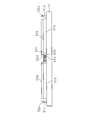
- 4A, 4B, 5A, 5B, 6A, 6B, and 7 are explanatory views for explaining a manufacturing process of the display device.
- 4A, 5A, 6A, and 7 are side views, and FIGS. 4B, 5B, and 6B are plan views.
- a UV-curable liquid resin 50 is applied onto the light guide plate 21 by dropping or coating.
- the resin 50 is coated so as to have a thickness equal to or greater than the total thickness of the optical sheets 23a, 23b, 23c, and 23d after being solidified.
- Resin 50 is coated along the two short sides and long sides of the light guide plate 21. Thereby, the two short side resin layers 51a and 51a are provided along the short side, and the two long side resin layers 51b and 51b are provided along the long side.
- the long side resin layers 51b and 51b are each provided with a gap at the center.
- Space holding layers 31a, 31a and 31b, 31b are formed by solidifying the short side resin layers 51a, 51a and the long side resin layers 51b, 51b by UV irradiation.
- the optical sheets 23a, 23b, 23c, and 23d are laminated on a wide surface of the light guide plate 21.
- the short side resin layers 51a and 51a and the long side resin layers 51b and 51b are solidified before the optical sheets 23a, 23b, 23c and 23d are laminated, and the tackiness of the surface is lost.
- optical sheets 23a, 23b, 23c, and 23d it is possible to prevent the optical sheets 23a, 23b, 23c, and 23d from unintentionally coming into contact with and being fixed to the short-side resin layers 51a and 51a and the long-side resin layers 51b and 51b before solidification. . Further, since the optical sheets 23a, 23b, 23c, and 23d are securely locked to the space holding layers 31a and 31b and the movement is restricted, the optical sheets 23a, 23b, 23c, and 23d can be accurately positioned.
- the convex portions are inserted into the gaps of the space holding layers 31, 31a, 31b, and 31b, respectively. Thereby, the optical sheets 23a, 23b, 23c, and 23d can be accurately positioned.
- a liquid resin 50 is further applied onto the space holding layers 31a, 31a, 31b, and 31b by dropping or coating.
- Short side resin layers 52a and 52a and long side resin layers 52b and 52b are provided.
- the liquid crystal panel 10 is placed and pressed from the surface side as shown by the arrows in FIG.
- the short side resin layers 52a and 52a and the long side resin layers 52b and 52b are solidified by UV irradiation to form the fixing layers 32a and 32a and 32b and 32b.
- a substrate 40 in which a light source 41 is arranged in parallel is attached to one side wall of the side plate 12b of the backlight chassis 12, and after a unit in which the liquid crystal panel 10 and the light guide plate 21 are coupled is carried into the backlight chassis 12, the bezel 11 is put on.
- the display device 1 is manufactured by fixing.
- the spacer 30 is formed, and the liquid crystal panel 10 and the light guide plate 21 are combined.
- the coated resin 50 can be easily solidified in a short time and the spacer 30 can be formed.
- the strength of fixing of the fixing layers 32 a and 32 b can be increased by pressing the liquid crystal panel 10. Further, the fixing layers 32a and 32b can be extended thinly, and the thickness of the spacer 30 can be made close to the thickness of the space holding layers 31a and 31b. Thereby, at the time of manufacture, the error between the actual thickness of the spacer 30 and the specified thickness can be reduced to the maximum allowable dimension or less, and the dimensional accuracy of the spacer 30 can be increased.
- the resin 50 that forms the short side resin layers 52a and 52a and the long side resin layers 52b and 52b is preferably a material that starts curing 1 to 5 minutes after UV irradiation. Since the resin 50 starts curing at least one minute after UV irradiation, the time required for forming the short side resin layers 52a and 52a and the long side resin layers 52b and 52b and placing the liquid crystal panel 10 is as follows. Can be secured. In addition, since the resin 50 starts to be cured at least 5 minutes after the UV irradiation, the display device can be manufactured efficiently.
- the resin 50 that forms the short side resin layers 52a and 52a and the long side resin layers 52b and 52b is more preferably a material that starts curing after 1 to 4 minutes from UV irradiation. Thereby, the display apparatus 1 can be manufactured more efficiently.
- the resin 50 that forms the short side resin layers 52a and 52a and the long side resin layers 52b and 52b is more preferably a material that starts curing after 1 to 3 minutes from UV irradiation. Thereby, the display apparatus 1 can be manufactured more efficiently.
- the space holding layers 31a and 31b are preferably 1300 to 1500 ⁇ m, and the fixing layers 32a and 32b are preferably 200 ⁇ m or less.
- the thickness of the fixing layers 32a and 32b is preferably 1/6 or less of the space holding layers 31a and 31b.
- the optical sheets 23a, 23b, 23c, and 23d may have a configuration in which no convex portion is provided. Even in this configuration, the optical sheets 23a, 23b, 23c, and 23d can be accurately positioned by the space holding layers 31a and 31b of the spacer 30.
- the resin is not limited to UV curable, and may be moisture curable or hot melt curable.
- the spacers 30 do not have to be formed continuously, and for example, the spacers 30 may be formed in a dot shape along each of the four sides of the light guide plate 21.
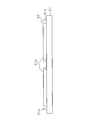
- FIG. 8 is a cross-sectional view showing a main part of the display device 1 according to the second embodiment.
- the thicknesses of the space holding layers 31a and 31b are the thicknesses of the three optical sheets 23a, 23b, and 23c excluding the optical sheet 23d that is closest to the liquid crystal panel 10 among the four optical sheets 23a, 23b, 23c, and 23d. Thicker than the total sum.
- the thickness of the space holding layers 31a and 31b is thinner than the total thickness of the four optical sheets 23a, 23b, 23c, and 23d.
- the space holding layers 31a and 31b hold the space in which the optical sheets 23a, 23b, and 23c are interposed. Further, a space for interposing another optical sheet 23d is secured by the thickness of the fixing layers 32a and 32b.
- the display device 1 according to the second embodiment can be manufactured by the same method as in the first embodiment. Further, since the optical sheets 23a, 23b, 23c, and 23d are locked to the space holding layers 31a, 31a and 31b, 31b and their movements are restricted, positioning can be performed accurately.
- the thickness of the space holding layer 31a is set to a minimum thickness that restricts the movement of the optical sheets 23a, 23b, 23c, and 23d, an increase in the thickness of the display device 1 due to the spacer can be suppressed.
- Display device 10 Liquid crystal panel (display panel) 21 Light guide plate 23a, 23b, 23c, 23d Optical sheet 30 Spacer 31a, 31b Space holding layer 32a, 32b Adhering layer 50 Resin (liquid)
Landscapes
- Physics & Mathematics (AREA)
- General Physics & Mathematics (AREA)
- Optics & Photonics (AREA)
- Engineering & Computer Science (AREA)
- Manufacturing & Machinery (AREA)
- Liquid Crystal (AREA)
Abstract
Priority Applications (3)
| Application Number | Priority Date | Filing Date | Title |
|---|---|---|---|
| PCT/JP2015/056080 WO2016139718A1 (fr) | 2015-03-02 | 2015-03-02 | Dispositif d'affichage et procédé de fabrication de dispositif d'affichage |
| JP2017503225A JP6456473B2 (ja) | 2015-03-02 | 2015-03-02 | 表示装置の製造方法 |
| US15/554,682 US10191211B2 (en) | 2015-03-02 | 2015-03-02 | Display apparatus and method of manufacturing the display apparatus |
Applications Claiming Priority (1)
| Application Number | Priority Date | Filing Date | Title |
|---|---|---|---|
| PCT/JP2015/056080 WO2016139718A1 (fr) | 2015-03-02 | 2015-03-02 | Dispositif d'affichage et procédé de fabrication de dispositif d'affichage |
Publications (1)
| Publication Number | Publication Date |
|---|---|
| WO2016139718A1 true WO2016139718A1 (fr) | 2016-09-09 |
Family
ID=56848425
Family Applications (1)
| Application Number | Title | Priority Date | Filing Date |
|---|---|---|---|
| PCT/JP2015/056080 Ceased WO2016139718A1 (fr) | 2015-03-02 | 2015-03-02 | Dispositif d'affichage et procédé de fabrication de dispositif d'affichage |
Country Status (3)
| Country | Link |
|---|---|
| US (1) | US10191211B2 (fr) |
| JP (1) | JP6456473B2 (fr) |
| WO (1) | WO2016139718A1 (fr) |
Cited By (1)
| Publication number | Priority date | Publication date | Assignee | Title |
|---|---|---|---|---|
| WO2019059353A1 (fr) * | 2017-09-25 | 2019-03-28 | シャープ株式会社 | Dispositif d'affichage et récepteur de télévision |
Families Citing this family (3)
| Publication number | Priority date | Publication date | Assignee | Title |
|---|---|---|---|---|
| CN105158968A (zh) * | 2015-07-30 | 2015-12-16 | 京东方科技集团股份有限公司 | 液晶显示模块及其制作方法、显示装置 |
| CN113156709B (zh) * | 2021-05-18 | 2025-06-27 | 北京京东方显示技术有限公司 | 一种背光模组及显示装置 |
| CN114999314A (zh) * | 2022-04-22 | 2022-09-02 | 鸿富锦精密工业(深圳)有限公司 | 多媒体装置 |
Citations (5)
| Publication number | Priority date | Publication date | Assignee | Title |
|---|---|---|---|---|
| JPH0996800A (ja) * | 1995-09-29 | 1997-04-08 | Toshiba Corp | 液晶表示装置 |
| US20070139583A1 (en) * | 2005-12-15 | 2007-06-21 | Tpo Hong Kong Holding Limited | Display module |
| JP2007232809A (ja) * | 2006-02-28 | 2007-09-13 | Casio Comput Co Ltd | 表示モジュール |
| JP2012118498A (ja) * | 2010-12-03 | 2012-06-21 | Wistron Corp | フラットパネルディスプレイ |
| JP2014142614A (ja) * | 2013-01-24 | 2014-08-07 | Lg Display Co Ltd | 液晶表示装置 |
Family Cites Families (3)
| Publication number | Priority date | Publication date | Assignee | Title |
|---|---|---|---|---|
| JP4801246B2 (ja) * | 2000-09-29 | 2011-10-26 | オプトレックス株式会社 | 液晶表示装置 |
| US20120092580A1 (en) * | 2010-10-13 | 2012-04-19 | Microsoft Corporation | Controlling spacing between display and reinforcement layer |
| KR102103904B1 (ko) * | 2013-04-30 | 2020-04-23 | 엘지디스플레이 주식회사 | 디스플레이 장치 |
-
2015
- 2015-03-02 WO PCT/JP2015/056080 patent/WO2016139718A1/fr not_active Ceased
- 2015-03-02 JP JP2017503225A patent/JP6456473B2/ja not_active Expired - Fee Related
- 2015-03-02 US US15/554,682 patent/US10191211B2/en not_active Expired - Fee Related
Patent Citations (5)
| Publication number | Priority date | Publication date | Assignee | Title |
|---|---|---|---|---|
| JPH0996800A (ja) * | 1995-09-29 | 1997-04-08 | Toshiba Corp | 液晶表示装置 |
| US20070139583A1 (en) * | 2005-12-15 | 2007-06-21 | Tpo Hong Kong Holding Limited | Display module |
| JP2007232809A (ja) * | 2006-02-28 | 2007-09-13 | Casio Comput Co Ltd | 表示モジュール |
| JP2012118498A (ja) * | 2010-12-03 | 2012-06-21 | Wistron Corp | フラットパネルディスプレイ |
| JP2014142614A (ja) * | 2013-01-24 | 2014-08-07 | Lg Display Co Ltd | 液晶表示装置 |
Cited By (1)
| Publication number | Priority date | Publication date | Assignee | Title |
|---|---|---|---|---|
| WO2019059353A1 (fr) * | 2017-09-25 | 2019-03-28 | シャープ株式会社 | Dispositif d'affichage et récepteur de télévision |
Also Published As
| Publication number | Publication date |
|---|---|
| JP6456473B2 (ja) | 2019-01-23 |
| JPWO2016139718A1 (ja) | 2017-12-14 |
| US20180039015A1 (en) | 2018-02-08 |
| US10191211B2 (en) | 2019-01-29 |
Similar Documents
| Publication | Publication Date | Title |
|---|---|---|
| JP5945070B1 (ja) | 表示装置及び表示装置の製造方法 | |
| CN106019666B (zh) | 显示装置及显示装置的制造方法 | |
| CN101493581A (zh) | 立体图像显示装置及其制造方法 | |
| JP2018004728A (ja) | 表示装置および接着方法 | |
| JP6456473B2 (ja) | 表示装置の製造方法 | |
| JP2017120310A (ja) | 表示装置、表示装置に用いる接着シート、および表示装置の製造方法 | |
| US20180129102A1 (en) | Liquid crystal display device and method of producing liquid crystal display device | |
| CN110609406A (zh) | 显示装置 | |
| CN102879941A (zh) | 液晶显示装置及其制造方法 | |
| US10203450B2 (en) | Backlight module and the manufacturing method thereof | |
| WO2016046971A1 (fr) | Dispositif d'affichage et procédé de fabrication de dispositif d'affichage | |
| TWM562990U (zh) | 背光模組及顯示裝置 | |
| CN206584142U (zh) | 显示装置 | |
| JP2008268420A (ja) | 液晶表示装置の製造方法 | |
| JP5756635B2 (ja) | 液晶素子 | |
| JP5946419B2 (ja) | 液晶表示装置の製造方法 | |
| TWI414429B (zh) | 防溢膠裝置及使用其之基板貼合方法 | |
| KR100997953B1 (ko) | 일체형 도광판 및 그 제조 방법 | |
| US11656397B2 (en) | Light guide for an electronic display and electronic display comprising said light guide | |
| JP4779859B2 (ja) | 液晶表示素子 | |
| JP6459051B2 (ja) | カバーガラスおよび補強部 | |
| KR100997956B1 (ko) | 일체형 도광판 및 그 제조 방법 | |
| JP5003349B2 (ja) | 電気光学装置の製造方法、電気光学装置の製造装置 | |
| JP2016014735A (ja) | 光学シートの製造方法および光学パネルの製造方法 | |
| JP2012208324A (ja) | 液晶素子 |
Legal Events
| Date | Code | Title | Description |
|---|---|---|---|
| 121 | Ep: the epo has been informed by wipo that ep was designated in this application |
Ref document number: 15883888 Country of ref document: EP Kind code of ref document: A1 |
|
| ENP | Entry into the national phase |
Ref document number: 2017503225 Country of ref document: JP Kind code of ref document: A |
|
| WWE | Wipo information: entry into national phase |
Ref document number: 15554682 Country of ref document: US |
|
| NENP | Non-entry into the national phase |
Ref country code: DE |
|
| 122 | Ep: pct application non-entry in european phase |
Ref document number: 15883888 Country of ref document: EP Kind code of ref document: A1 |