WO2019065244A1 - 磁気センサの製造方法及び磁気センサ集合体 - Google Patents
磁気センサの製造方法及び磁気センサ集合体 Download PDFInfo
- Publication number
- WO2019065244A1 WO2019065244A1 PCT/JP2018/033810 JP2018033810W WO2019065244A1 WO 2019065244 A1 WO2019065244 A1 WO 2019065244A1 JP 2018033810 W JP2018033810 W JP 2018033810W WO 2019065244 A1 WO2019065244 A1 WO 2019065244A1
- Authority
- WO
- WIPO (PCT)
- Prior art keywords
- magnetic
- magnetic sensor
- layer
- substrate
- sensing
- Prior art date
- Legal status (The legal status is an assumption and is not a legal conclusion. Google has not performed a legal analysis and makes no representation as to the accuracy of the status listed.)
- Ceased
Links
Images


Classifications
-
- G—PHYSICS
- G01—MEASURING; TESTING
- G01R—MEASURING ELECTRIC VARIABLES; MEASURING MAGNETIC VARIABLES
- G01R33/00—Arrangements or instruments for measuring magnetic variables
- G01R33/0052—Manufacturing aspects; Manufacturing of single devices, i.e. of semiconductor magnetic sensor chips
-
- C—CHEMISTRY; METALLURGY
- C23—COATING METALLIC MATERIAL; COATING MATERIAL WITH METALLIC MATERIAL; CHEMICAL SURFACE TREATMENT; DIFFUSION TREATMENT OF METALLIC MATERIAL; COATING BY VACUUM EVAPORATION, BY SPUTTERING, BY ION IMPLANTATION OR BY CHEMICAL VAPOUR DEPOSITION, IN GENERAL; INHIBITING CORROSION OF METALLIC MATERIAL OR INCRUSTATION IN GENERAL
- C23C—COATING METALLIC MATERIAL; COATING MATERIAL WITH METALLIC MATERIAL; SURFACE TREATMENT OF METALLIC MATERIAL BY DIFFUSION INTO THE SURFACE, BY CHEMICAL CONVERSION OR SUBSTITUTION; COATING BY VACUUM EVAPORATION, BY SPUTTERING, BY ION IMPLANTATION OR BY CHEMICAL VAPOUR DEPOSITION, IN GENERAL
- C23C14/00—Coating by vacuum evaporation, by sputtering or by ion implantation of the coating forming material
- C23C14/06—Coating by vacuum evaporation, by sputtering or by ion implantation of the coating forming material characterised by the coating material
-
- C—CHEMISTRY; METALLURGY
- C23—COATING METALLIC MATERIAL; COATING MATERIAL WITH METALLIC MATERIAL; CHEMICAL SURFACE TREATMENT; DIFFUSION TREATMENT OF METALLIC MATERIAL; COATING BY VACUUM EVAPORATION, BY SPUTTERING, BY ION IMPLANTATION OR BY CHEMICAL VAPOUR DEPOSITION, IN GENERAL; INHIBITING CORROSION OF METALLIC MATERIAL OR INCRUSTATION IN GENERAL
- C23C—COATING METALLIC MATERIAL; COATING MATERIAL WITH METALLIC MATERIAL; SURFACE TREATMENT OF METALLIC MATERIAL BY DIFFUSION INTO THE SURFACE, BY CHEMICAL CONVERSION OR SUBSTITUTION; COATING BY VACUUM EVAPORATION, BY SPUTTERING, BY ION IMPLANTATION OR BY CHEMICAL VAPOUR DEPOSITION, IN GENERAL
- C23C14/00—Coating by vacuum evaporation, by sputtering or by ion implantation of the coating forming material
- C23C14/22—Coating by vacuum evaporation, by sputtering or by ion implantation of the coating forming material characterised by the process of coating
- C23C14/34—Sputtering
- C23C14/35—Sputtering by application of a magnetic field, e.g. magnetron sputtering
-
- G—PHYSICS
- G01—MEASURING; TESTING
- G01R—MEASURING ELECTRIC VARIABLES; MEASURING MAGNETIC VARIABLES
- G01R33/00—Arrangements or instruments for measuring magnetic variables
- G01R33/02—Measuring direction or magnitude of magnetic fields or magnetic flux
-
- H—ELECTRICITY
- H01—ELECTRIC ELEMENTS
- H01F—MAGNETS; INDUCTANCES; TRANSFORMERS; SELECTION OF MATERIALS FOR THEIR MAGNETIC PROPERTIES
- H01F10/00—Thin magnetic films, e.g. of one-domain structure
- H01F10/08—Thin magnetic films, e.g. of one-domain structure characterised by magnetic layers
-
- H—ELECTRICITY
- H01—ELECTRIC ELEMENTS
- H01F—MAGNETS; INDUCTANCES; TRANSFORMERS; SELECTION OF MATERIALS FOR THEIR MAGNETIC PROPERTIES
- H01F41/00—Apparatus or processes specially adapted for manufacturing or assembling magnets, inductances or transformers; Apparatus or processes specially adapted for manufacturing materials characterised by their magnetic properties
- H01F41/32—Apparatus or processes specially adapted for manufacturing or assembling magnets, inductances or transformers; Apparatus or processes specially adapted for manufacturing materials characterised by their magnetic properties for applying conductive, insulating or magnetic material on a magnetic film, specially adapted for a thin magnetic film
-
- G—PHYSICS
- G01—MEASURING; TESTING
- G01R—MEASURING ELECTRIC VARIABLES; MEASURING MAGNETIC VARIABLES
- G01R33/00—Arrangements or instruments for measuring magnetic variables
- G01R33/02—Measuring direction or magnitude of magnetic fields or magnetic flux
- G01R33/06—Measuring direction or magnitude of magnetic fields or magnetic flux using galvano-magnetic devices
- G01R33/09—Magnetoresistive devices
- G01R33/093—Magnetoresistive devices using multilayer structures, e.g. giant magnetoresistance sensors
Definitions
- the present invention relates to a method of manufacturing a magnetic sensor and a magnetic sensor assembly.
- a magnetic detection element utilizing magnetic impedance effect which is configured by forming a high permeability magnetic film on a nonmagnetic substrate, and the high permeability magnetic film is along the magnetic field detection direction.
- a plurality of linear portions are arranged in parallel at predetermined intervals, connected in series so as to be sequentially folded back, and formed in a serpentine pattern electrically connected in series, and the direction of easy magnetization axis is in the film plane with respect to the magnetic field detection direction.
- Magnetic anisotropy is applied so that the direction is perpendicular, high frequency current is applied from both ends of the high permeability magnetic film, and change in impedance generated between the both ends by an external magnetic field is converted into an electric signal
- a magnetic detection element capable of obtaining an output (see Patent Document 1).
- a strip-like soft magnetic material to which uniaxial anisotropy is imparted in the short direction, is used as the sensing part.
- the uniaxial anisotropy of the soft magnetic material is applied by heat treatment in a magnetic field or the like after the sensing portion is formed.
- the present invention provides a method of manufacturing a magnetic sensor, etc., in which the steps required for manufacturing are simplified as compared to the case of using heat treatment in a magnetic field.
- a method of manufacturing a magnetic sensor to which the present invention is applied includes a soft magnetic material layer depositing step of depositing a soft magnetic material layer constituting a sensing unit for sensing a magnetic field on a substrate by magnetron sputtering; And a sensing portion forming step of forming a sensing portion for sensing a magnetic field at a portion to which uniaxial magnetic anisotropy is imparted by the magnetic field used for sputtering.
- the sensing portion is formed such that the short direction of the sensing portion having the longitudinal direction and the short direction is directed to the direction of uniaxial magnetic anisotropy. It can be done.
- the magnetron sputtering can be characterized in that it is performed using a cathode in which a magnet forming a magnetic field rotates in a plane facing the surface of the substrate. Furthermore, in a method of manufacturing such a magnetic sensor, for a substrate provided with a thin film magnet made of a hard magnetic material, which forms a magnetic field in a direction intersecting the direction of uniaxial magnetic anisotropy of the sensing part, The method may be characterized in that a soft magnetic layer deposition step and a sensing portion formation step are performed.
- the sensing unit that senses the magnetic field is the magnetic field formed in the magnetron sputtering used to form the soft magnetic material layer that constitutes the sensing unit.
- the sensing unit comprises a plurality of magnetic sensors each arranged.
- Each sensing part of a plurality of magnetic sensors in such a magnetic sensor assembly has a longitudinal direction and a short direction, and the short direction is directed to the direction of the magnetic field formed in the magnetron sputtering. It can be done.
- each of the plurality of magnetic sensors may be characterized by including a thin film magnet made of a hard magnetic material that forms a magnetic field in a direction intersecting the direction of uniaxial magnetic anisotropy of the sensing part.
- FIG. 1 It is a figure explaining an example of the magnetic sensor to which a 1st embodiment is applied.
- (A) is a plan view
- (b) is a cross-sectional view taken along line IB-IB in (a).
- (A) to (c) show steps in a method of manufacturing a magnetic sensor. It is a sectional view explaining an outline of a magnetron sputtering device. It is a figure which shows the structure of the magnetic circuit in a magnetron sputtering device, and arrangement
- (A) shows the configuration of the magnetic circuit viewed from the target side, and (b) shows the arrangement of the magnetic sensor formed on the substrate (magnetic sensor assembly). It is a figure which shows the modification 1 of the magnetic circuit in a magnetron sputtering device, and arrangement
- (A) shows the structure of the magnetic circuit of the modification 1 seen from the target side,
- (b) shows arrangement
- substrate shows the structure of modification 2 of the magnetic circuit in a magnetron sputtering device, and arrangement
- FIG. It is a figure explaining an example of the magnetic sensor to which a 2nd embodiment is applied.
- (A) is a plan view, (b) is a cross-sectional view taken along the line VIIB-VIIB of (a). It is a figure explaining an example of the magnetic sensor to which a 3rd embodiment is applied.
- (A) is a plan view, (b) is a cross-sectional view taken along line VIIIB-VIIIB of (a). It is a figure explaining an example of the magnetic sensor to which a 4th embodiment is applied.
- (A) is a plan view
- (b) is a cross-sectional view taken along line IXB-IXB of (a). It is a figure explaining an example of the manufacturing method of the magnetic sensor to which a 4th embodiment is applied.
- (A) to (g) show steps in a method of manufacturing a magnetic sensor. It is a figure explaining an example of the magnetic sensor to which a 5th embodiment is applied.
- (A) is a plan view
- (b) is a cross-sectional view taken along line XIB-XIB of (a).
- (A) is a plan view
- (b) is a cross-sectional view taken along the line XIIB-XIIB in (a).
- FIG. 1 is a diagram for explaining an example of a magnetic sensor 1 to which the first embodiment is applied.
- 1 (a) is a plan view
- FIG. 1 (b) is a cross-sectional view taken along line IB-IB in FIG. 1 (a).
- the magnetic sensor 1 is provided on a substrate 10 and a substrate 10, and a magnetic sensor main body 20 formed of a soft magnetic material (soft magnetic material layer 101 described later).
- a soft magnetic material soft magnetic material layer 101 described later.
- the magnetic sensor main body 20 includes a plurality of sensing units 21 for sensing changes in a magnetic field (external magnetic field), and a connection unit 22 for connecting the plurality of sensing units 21 in series (striking). And a terminal unit 23 to which a wire for supplying a current to the sensing unit 21 is connected.
- the soft magnetic material layer 101 that constitutes the sensing unit 21 is written in parentheses. The same is true for the other cases.
- the soft magnetic material is a material having a so-called small coercivity, which is easily magnetized by an external magnetic field, but quickly returns to its original state without magnetization or small when the external magnetic field is removed.
- the soft magnetic material for example, an amorphous alloy obtained by adding high melting point metal Nb, Ta, W or the like to an alloy containing Co as a main component (hereinafter referred to as a Co alloy constituting the sensing portion 21) can be used.
- the Co alloy constituting the sensing portion 21 include CoNbZr, CoFeTa, CoWZr and the like. In the present specification, the composition ratio of the alloy is not particularly shown. The same applies to the following.
- the substrate 10 is a substrate made of a nonmagnetic material, and for example, an oxide substrate such as glass or sapphire, or a semiconductor substrate such as silicon can be used.
- the substrate 10 is described as being glass.
- the substrate 10 is, for example, a disc having a diameter of about 95 mm and a thickness of about 0.5 mm.
- FIG. 1 shows one magnetic sensor 1 cut out.
- an electrical insulating layer may be provided on the substrate 10.
- the sensing unit 21 is a strip-shaped member which is formed of a soft magnetic layer 101 described later and in which current flows in the longitudinal direction.
- a plurality of sensing portions 21 are arranged (arranged) in parallel in the longitudinal direction.
- the number of sensing units 21 may be one.
- connection portion 22 is formed of the soft magnetic layer 101 and is provided between the end portions of the adjacent sensing portions 21. And the connection part 22 connects several sensing part 21 in series (striking). Here, since there are four sensing portions 21, there are three connecting portions 22. When the number of sensing units 21 is two, the number of connection units 22 may be one. When the number of the sensing units 21 is one, the connection unit 22 may not be provided. The width of the connection portion 22 may be the same as that of the sensing portion 21.
- the terminal portion 23 is formed of the soft magnetic layer 101, and provided at each end (two) of the sensing portion 21 not connected by the connection portion 22.
- the terminal portion 23 includes a lead-out portion drawn from the sensing portion 21 and a portion (pad) to which a wire for supplying an electric current is connected.
- the part which connects an electric wire should just be a magnitude
- the sensing portion 21, the connection portion 22, and the terminal portion 23 are formed by processing the same soft magnetic layer 101 and are continuous.
- the magnetic sensor 1 is imparted with uniaxial magnetic anisotropy in which the axis of easy magnetization is oriented in the short direction (width direction) intersecting the longitudinal direction of the sensing unit 21.
- a bias magnetic field generated by, for example, flowing a current through a coil is applied so that a magnetic flux is transmitted from the outside in the longitudinal direction of the sensing unit 21.
- a high frequency current is caused to flow from the two terminal portions 23 to the sensing portion 21 to measure the resistance value (impedance) between the terminal portions 23.
- the resistance value (impedance) between the terminal portions 23 senses a component in the direction along the longitudinal direction of the sensing portion 21 of the external magnetic field. Therefore, from the measurement of the resistance value (impedance) between the terminal portions 23, the change of the external magnetic field or the external magnetic field is measured.
- the bias magnetic field is set to a state in which a change in resistance (impedance) between the terminal portions 23 is large with respect to a change in the external magnetic field. That is, by applying a bias magnetic field and using a steep portion of the impedance change with respect to the external magnetic field, it is possible to capture a weak external magnetic field change.
- the sensing portion 21 has a width of several tens of ⁇ m in the lateral direction, a length of about 1 mm in the longitudinal direction, and a thickness of 0.5 to 5 ⁇ m.
- the distance between the two sensing portions 21 arranged (arranged) in parallel is 50 to 100 ⁇ m. Therefore, the planar shape of the magnetic sensor 1 is several mm square. Other values may be used depending on the value of the external magnetic field to be measured and the soft magnetic material to be used.
- FIG. 2 is a diagram for explaining an example of a method of manufacturing the magnetic sensor 1.
- FIGS. 2A to 2C show steps in the method of manufacturing the magnetic sensor 1.
- 2 (a) to 2 (c) are representative steps and proceed in the order of FIGS. 2 (a) to 2 (c).
- 2 (a) to 2 (c) correspond to the cross-sectional view of FIG. 1 (b).
- FIG. 2A is a step of forming a resist pattern, and a resist pattern 201 for lifting off the soft magnetic layer 101 deposited in the following FIG. 2B is formed on the substrate 10.
- a resist pattern 201 having a portion where the magnetic sensor main body 20 is to be formed as an opening on one surface (hereinafter referred to as the surface) of the substrate 10 is a known photo Formed by lithography.
- the sensing unit 21 of the magnetic sensor main body 20 is disposed in a magnetic field used in a magnetron sputtering apparatus 300 (magnetron sputtering apparatus 300) described later, and the width direction of the sensing unit 21 ( The width direction is formed to be directed to the direction of the magnetic field.
- the short direction is the direction of the magnetic field means that the angle between the direction of the magnetic field and the short direction is less than 45 °. The smaller the angle between the direction of the magnetic field and the short direction, the better.
- FIG. 2B is a step of depositing the soft magnetic layer, and a layer (soft magnetic layer 101) of the soft magnetic material is deposited on the surface of the substrate 10 on which the resist pattern 201 is formed.
- the soft magnetic material layer 101 is deposited on the substrate 10 by the magnetron sputtering apparatus 300 using a target made of a soft magnetic material (target shown in FIG. 3 described later).
- the soft magnetic material is a Co alloy that constitutes the above-described sensing unit 21.
- the deposition of the soft magnetic layer 101 and the like by the magnetron sputtering apparatus 300 may be described as depositing the soft magnetic layer 101 and the like by magnetron sputtering.
- FIG. 2C is a soft magnetic body layer lift-off step, in which the soft magnetic body layer 101 deposited on the substrate 10 is lifted off and the magnetic sensor main body 20 including the sensing portion 21, the connection portion 22 and the terminal portion 23. Processed into Here, by removing the resist pattern 201, the soft magnetic layer 101 deposited on the resist pattern 201 is removed. As a result, the soft magnetic layer 101 remains in the opening of the resist pattern 201. Thus, the magnetic sensor main body 20 is formed.
- the soft magnetic material layer lift-off process is an example of the sensing unit formation process. When using an etching method, the process of forming the sensing part 21 by etching becomes a sensing part formation process.
- the sensing part 21 of the magnetic sensor main body 20 is in the magnetic field of the magnetron sputtering apparatus 300, and the short side direction (width direction) of the sensing part 21 is directed to the direction of the magnetic field of the magnetron sputtering apparatus 300. It is done. Therefore, the soft magnetic layer 101 is imparted with uniaxial magnetic anisotropy in which the axis of easy magnetization is oriented in the lateral direction (width direction) of the sensing portion 21 during film formation (deposition). That is, uniaxial magnetic anisotropy is induced and imparted by the magnetic field of the magnetron sputtering apparatus 300. Therefore, this uniaxial magnetic anisotropy may be described as induced magnetic anisotropy. Thus, it is not necessary to perform heat treatment in a magnetic field after the magnetic sensor 1 is formed.
- the heat treatment in a magnetic field is, for example, a heat treatment at 400 ° C. in a rotating magnetic field of 3 kG (0.3 T) and a heat treatment at 400 ° C. in a static magnetic field of 3 kG (0.3 T) following it. That is, in the method of manufacturing the magnetic sensor 1 to which the first embodiment is applied, the heat treatment in the magnetic field at a high temperature such as 400 ° C. is not required.
- FIG. 3 is a cross-sectional view for explaining the outline of the magnetron sputtering apparatus 300.
- the magnetron sputtering apparatus 300 here is cylindrical with the OO line of FIG. 3 as the axis of rotation.
- the magnetron sputtering apparatus 300 includes a barrier rib 310 and a magnetron cathode 320.
- the partition wall 310 and the magnetron cathode 320 constitute a chamber 340 which is a sealed space via an insulating member 311 such as polytetrafluoroethylene.
- a substrate holder 350 for holding the substrate 10 is provided in the chamber 340.
- the partition wall 310 is grounded (GND).
- the substrate holder 350 is grounded (GND) through the partition wall 310 and functions as an anode. That is, the high frequency power supply 360 is connected between the grounded substrate holder 350 and the magnetron cathode 320.
- a direct current power supply may be connected instead of the high frequency power supply 360, and direct current (DC) may be applied between the substrate holder 350 and the magnetron cathode 320.
- a vacuum pump for reducing the pressure in the chamber 340 a gas supply mechanism for introducing a gas used for sputtering, such as Ar, etc.
- a pressure adjusting mechanism is provided to hold the pressure in the chamber 340 at a predetermined value.
- a cooling mechanism for supplying a cooling liquid to the magnetron cathode 320 may be provided to cool the magnetron cathode 320.
- a heating mechanism for heating the substrate 10, for example, an infrared lamp, or a cooling mechanism for supplying a cooling liquid to the substrate holder 350 for cooling the substrate 10 may be provided.
- the magnetron cathode 320 transmits a cathode housing 321, a target 322 which is a thin film material formed on the substrate 10, a backing plate 323 holding the target 322, and the backing plate 323 to generate a magnetic field on the target 322 side.
- a magnetic circuit 330 is provided.
- the target 322 is made of a Co alloy that constitutes the above-described sensing unit 21.
- the backing plate 323 is made of oxygen-free copper or the like having high conductivity. Then, the target 322 is fixed to the surface with a conductive adhesive or the like.
- the cathode housing 321 is made of stainless steel or the like.
- the backing plate 323 to which the target 322 is attached is fixed to the cathode housing 321, and the magnetic circuit 330 is provided on the side of the backing plate 323 where the target 322 is not provided.
- the size (diameter) of the target 322 is set such that a film is formed (deposited) in a predetermined area (range) of the substrate 10. Here, the diameter of the target 322 is larger than the diameter of the substrate 10.
- the magnetic circuit 330 is provided on the side opposite to the backing plate 323 side of the magnet (magnet) 331 with the N pole exposed on the backing plate 323 side, the magnet 332 with the S pole exposed, and the magnets 331 and 332.
- a yoke 333 for guiding the magnetic flux from the north pole of the magnet to the south pole of the magnet 331 is provided.
- permanent magnets are used for the magnets 331 and 332.
- the magnets 331 and 332 are concentrically provided so that the magnet 331 with the exposed N pole on the backing plate 323 side is outside and the magnet 332 with the exposed S pole is inside. It is done.
- magnetic lines of force (indicated by arrows) from the N pole of the magnet 331 to the S pole of the magnet 332 pass through the backing plate 323 and the target 322 and are generated in the chamber 340. Then, a part of the magnetic force lines reach the substrate 10 held by the substrate holder 350, and passes the substrate 10 in a direction parallel to the surface. That is, in the substrate 10, a magnetic field in a direction parallel to the surface is generated at the portion through which the magnetic lines of force pass. That is, uniaxial magnetic anisotropy is imparted with the deposition of the soft magnetic layer 101 deposited (formed) on the substrate 10 by the magnetic field in the direction parallel to the surface generated on the substrate 10.
- the magnetron sputtering apparatus 300 electrons generated by the discharge generated by the high frequency power supply 360 are concentrated (confined) in the vicinity of the target 322 by magnetic lines of force on the surface of the target 322. As a result, the collision probability between the electrons and the gas is increased to promote the ionization of the gas, and the deposition rate (film forming rate) of the film is improved. Note that the surface of the target 322 where electrons are concentrated by magnetic lines of force is in a range where it is eroded (eroded) by the impact of ions of the ionized gas.
- the substrate holder 350 is made of stainless steel or the like. Then, the substrate holder 350 holds the substrate 10 by a mechanism (not shown) for holding the substrate 10. As mentioned above, the magnetron sputtering apparatus 300 is cylindrical. And the target 322 is also circular (disk shape). The substrate 10 is also circular (disk-like), and is held by the substrate holder 350 so as to face the target 322 (see FIG. 4 described later).
- the magnetron sputtering apparatus 300 shown in FIG. 3 is a single-wafer sputtering apparatus for forming (depositing) a film for each so-called substrate 10. Further, in the magnetron sputtering apparatus 300 shown in FIG. 3, the surface of the substrate 10 (the surface of the target 322) is arranged horizontally (in the horizontal direction in the plane of FIG. 3). May be arranged in the direction).
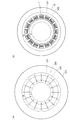
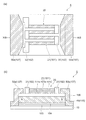
- FIG. 4 is a view showing the configuration of the magnetic circuit 330 in the magnetron sputtering apparatus 300 and the arrangement (magnetic sensor assembly) of the magnetic sensor 1 formed on the substrate 10.
- FIG. 4A shows the configuration of the magnetic circuit 330 viewed from the target 322 side
- FIG. 4B shows the arrangement (magnetic sensor assembly) of the magnetic sensor 1 formed on the substrate 10.
- the target 322 is circular.
- the magnetic circuit 330 viewed through the target 322 is provided with the N pole of the magnet 331 and the S pole of the magnet 332 concentrically. Then, magnetic lines of force (arrows) passing from the N pole of the magnet 331 to the S pole of the magnet 332 through the target 322 are formed.
- substrate 10 is disk shape provided facing the target 322.
- FIG. 4B the positions of the magnets 331 and 332 of the opposing magnetic circuit 330 are shown.
- the lateral direction (width direction) of the sensing portion 21 formed of the soft magnetic material layer 101 faces in the passing direction of the magnetic lines of force.
- the width direction of the sensing portion 21 is in the radial direction of the circle inside the circle formed by the N pole of the magnet 331 and the S pole of the magnet 332 in the magnetic circuit 330. It is arranged (arranged) along the side.
- one magnetic sensor 1 is described between the circle formed by the N pole of the magnet 331 and the circle formed by the S pole of the magnet 332 in the magnetic circuit 330. This is to explain the relationship between the sensing portion 21 of the magnetic sensor 1 and the magnetic field generated by the N pole of the magnet 331 and the S pole of the magnet 332.
- the magnetic sensor 1 is disposed so that the short side direction of the sensing unit 21 in the magnetic sensor main body 20 is along the direction of the magnetic field.
- a plurality of magnetic sensors 1 are arranged along the circumferential direction.
- the planar shape of the magnetic sensor 1 is several mm square as described above. Therefore, the plurality of magnetic sensors 1 are disposed in the direction of the magnetic field formed by the N pole of the magnet 331 and the S pole of the magnet 332 in practice. The same applies to the circumferential direction.
- the central portion and the outer peripheral portion of the substrate 10 are not easily affected by the magnetic field generated by the magnetic circuit 330. That is, uniaxial magnetic anisotropy is hardly imparted to the soft magnetic layer 101 by the magnetic field generated by the magnetic circuit 330.
- substrate 10 should just be an area
- a magnetic field is strong between the N pole of the magnet 331 and the S pole of the magnet 332. Therefore, it is preferable to arrange the magnetic sensor 1 between the N pole of the magnet 331 and the S pole of the magnet 332.
- the region in which the magnetic sensor 1 is disposed may not be between the N pole of the magnet 331 and the S pole of the magnet 332. Therefore, it is preferable not to arrange the magnetic sensor 1 in the central portion or the outer peripheral portion of the substrate 10 to which uniaxial magnetic anisotropy is hard to be imparted. However, in the case where the magnetic sensor 1 is disposed at the central portion or the outer peripheral portion of the substrate 10, the magnetic sensor 1 disposed at the central portion or the outer peripheral portion of the substrate 10 If you can be disposed at the central portion or the outer peripheral portion of the substrate 10.
- the magnetic sensor 1 may be shipped with the substrate 10 on which a plurality of magnetic sensors 1 are formed. That is, at the shipping destination, the substrate 10 is divided (cut) into individual magnetic sensors 1.
- the substrate 10 may be a part.
- FIG. 4B shows a magnetic sensor assembly in which the individual magnetic sensors 1 are not cut out from the substrate 10.
- the adhesive sheet is stretched so that the magnetic sensor 1 can be easily taken out. It may be.
- the magnetic sensor 1 can also be shipped in such a state. That is, the individual magnetic sensors 1 are taken out from the adhesive tape at the shipping destination.
- the substrate 10 may be a part.
- the magnetic sensor 1 is arranged in a state reflecting the arrangement of the magnets 331 and 332 of the magnetic circuit 330 in the magnetron cathode 320 of the magnetron sputtering apparatus 300 forming the soft magnetic layer 101. .
- the deposition rate of the soft magnetic layer 101 is improved by using the magnetron sputtering apparatus 300 for forming (depositing) the soft magnetic layer 101, and deposition ( The required time for the film is shortened, and uniaxial magnetic anisotropy is given simultaneously with the deposition of the soft magnetic layer 101. Therefore, in the manufacture of the magnetic sensor 1, the heat treatment step in the magnetic field for giving uniaxial magnetic anisotropy is unnecessary, and the steps required for the manufacture are simplified.
- FIG. 5 is a view showing a modification 1 of the magnetic circuit 330 in the magnetron sputtering apparatus 300 and the arrangement (magnetic sensor assembly) of the magnetic sensor 1 formed on the substrate 10.
- FIG. 5A shows the configuration of the magnetic circuit 330 of the first modification viewed from the target 322 side
- FIG. 5B shows the arrangement (magnetic sensor assembly) of the magnetic sensor 1 formed on the substrate 10.
- the planar shape of the target 322 in the magnetic circuit 330 of the modification 1 is a rectangle. That is, in the magnetron sputtering apparatus 300 provided with the magnetic circuit 330 of the modified example 1, the chamber 340 is not cylindrical but has a prismatic shape. The other configuration is the same as that of the magnetron sputtering apparatus 300 shown in FIG. Therefore, the description of the same part is omitted.
- the magnetic circuit 330 of the first modification viewed through the target 322 has the N pole of the magnet 331 provided along the side of the rectangle inside the rectangular target 322 and the S pole of the magnet 332 inside the rectangle Are arranged (arranged) along the side of.
- the substrate 10 is a rectangle provided to face the target 322.
- FIG. 5B the positions of the magnets 331 and 332 of the opposing magnetic circuit 330 are shown.
- the magnetic sensor 1 at the portion where magnetic lines of force pass on the substrate 10, the lateral direction (width direction) of the sensing portion 21 formed of the soft magnetic material layer 101 in the passing direction of magnetic lines of force (direction of magnetic field) It is arranged to face. That is, the magnetic sensor 1 is provided inside the magnetic field produced by the N pole of the magnet 331 of the magnetic circuit 330 and the S pole of the magnet 332 so that the short side direction (width direction) of the sensing portion 21 follows the direction of the magnetic field. It is done.
- one magnetic sensor 1 is described between the N pole of the magnet 331 and the S pole of the magnet 332 in the magnetic circuit 330. This is to explain the relationship between the sensing portion 21 of the magnetic sensor 1 and the magnetic field generated by the N pole of the magnet 331 and the S pole of the magnet 332.
- the magnetic sensor 1 is disposed along the rectangular side provided with the magnets 331 and 332 so that the short side direction of the sensing unit 21 in the magnetic sensor main body 20 follows the direction of the magnetic field.
- the planar shape of the magnetic sensor 1 is several mm square as described above. Therefore, a plurality of magnetic sensors 1 are disposed between the N pole of the magnet 331 and the S pole of the magnet 332. The same applies to the direction along the sides of the rectangle on which the magnets 331 and 332 are provided.
- FIG. 5B shows a magnetic sensor assembly in which the individual magnetic sensors 1 are not cut out from the substrate 10.
- the adhesive sheet is stretched so that the magnetic sensor 1 can be easily taken out. It may be.
- the magnetic sensor 1 can also be shipped in such a state. That is, the individual magnetic sensors 1 are taken out from the adhesive tape at the shipping destination.
- the substrate 10 may be a part.
- the magnetic sensor 1 is arranged in a state reflecting the arrangement of the magnets 331 and 332 of the magnetic circuit 330 in the magnetron cathode 320 of the magnetron sputtering apparatus 300 forming the soft magnetic layer 101. .
- the substrate 10 is rectangular so as to correspond to the planar shape of the target 322.
- the substrate 10 may be circular as shown in FIG. 4 (b).
- the plurality of magnetic sensors 1 may be disposed corresponding to the magnetic field generated by the N pole of the magnet 331 of the magnetic circuit 330 and the S pole of the magnet 332.
- the magnets 331 and 332 constituting the magnetic circuit 330 of the first modification are rectangular, but may be square or polygonal. Then, the short side direction of the sensing portion 21 of the magnetic sensor 1 to be manufactured may be disposed in the direction of the magnetic field generated by the magnets 331 and 332.
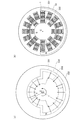
- FIG. 6 is a view showing the configuration of a modification 2 of the magnetic circuit 330 in the magnetron sputtering apparatus 300 and the arrangement (magnetic sensor assembly) of the magnetic sensor 1 formed on the substrate 10.
- FIG. 6A shows the configuration of the magnetic circuit 330 of the second modification viewed from the target 322 side
- FIG. 6B shows the arrangement (magnetic sensor assembly) of the magnetic sensor 1 formed on the substrate 10.
- the target 322 has a disk shape and the magnet 331 surrounds the magnet 332, as in the magnetic circuit 330 shown in FIG. It is provided.
- the magnet 331 is configured such that the end thereof includes a portion of the distance ⁇ and a portion of the distance ⁇ shorter than the distance ⁇ from the center C of the target 322 ( ⁇ > ⁇ ).
- the distances ⁇ between the magnet 331 and the magnet 332 are approximately equal.
- the other structure of the magnetron sputtering device 300 provided with the magnetic circuit 330 of the modification 2 is the same as that of the magnetron sputtering device 300 shown in FIG. Therefore, the description of the same part is omitted.
- the magnet 331 and the magnet 332 maintain this state, and rotate about the center C of the target 322 as a rotation axis.
- the magnetic circuit 330 provided with the magnets 331 and 332 rotates, and the target 322 (backing plate 323) does not rotate. That is, on the back surface of the target 322 (backing plate 323), the magnetic circuit 330 is a virtual surface parallel to the surface of the target 322 (backing plate 323) (the end of the N pole of the magnet 331 and the S pole of the magnet 332). Rotate in the plane including the end).
- the magnetic circuit 330 rotates in a plane parallel to the surface of the substrate 10. Note that rotation in the plane parallel to the substrate 10 is not necessarily required, and rotation may be performed in the plane opposite to the surface of the substrate 10.
- a magnetic field generated from the center C at a distance ⁇ and a distance ⁇ - ⁇ and a magnetic field generated from a distance ⁇ and a distance ⁇ - ⁇ are alternately generated on the target 322.
- the area (area) in which the electrons are captured is expanded compared to the case shown in FIG. 4 (a).
- the range in which the target 322 is eroded (eroded) by the impact of ions is extended, and the use efficiency of the target 322 is increased.
- the magnetic sensor 1 has the soft magnetic material layer 101 in the direction (the direction of the magnetic field) through which the lines of magnetic force pass in the portion of the magnetic circuit 330 through which the lines of magnetic force generated by the magnets 331 and 332 pass.
- the magnetic sensor 1 has a circle whose radius is the maximum distance from the center C to the N pole of the magnet 331, that is, a circle from the center C to the S pole of the magnet 332. It is disposed between the circle and the radius of the minimum distance of.
- the number of magnetic sensors 1 that can be manufactured on the substrate 10 is increased compared to the case shown in FIG. In FIG. 6B, the positions of the magnets 331 and 332 of the opposing magnetic circuit 330 are shown.
- the magnetic sensor 1 is disposed along the circumference such that the short direction of the sensing unit 21 in the magnetic sensor main body 20 follows the direction of the magnetic field.
- the planar shape of the magnetic sensor 1 is several mm square as described above. Therefore, the plurality of magnetic sensors 1 are disposed in the direction (diameter direction) of the magnetic field generated by the N pole of the magnet 331 and the S pole of the magnet 332. The same applies to the circumferential direction.
- FIG. 6B shows a magnetic sensor assembly in which the individual magnetic sensors 1 are not cut out from the substrate 10.
- the adhesive sheet is stretched so that the magnetic sensor 1 can be easily taken out. It may be.
- the magnetic sensor 1 can also be shipped in such a state. That is, the individual magnetic sensors 1 are taken out from the adhesive tape at the shipping destination.
- the substrate 10 may be a part.
- the individual magnetic sensors 1 are disposed in a state reflecting the arrangement of the magnets 331 and 332 of the magnetic circuit 330 in the magnetron cathode 320 of the magnetron sputtering apparatus 300 forming the soft magnetic layer 101. ing.
- the arrangement and shape of the magnets 331 and 332 constituting the magnetic circuit 330 may be other than the arrangement and shape shown in FIG.
- the area where the uniaxial magnetic anisotropy of the soft magnetic layer 101 formed on the substrate 10 can be obtained may be set to be expanded.
- connection portion 22 and the terminal portion 23 are made of a conductive material.
- parts different from the first embodiment will be mainly described, and the same parts will be denoted by the same reference numerals and descriptions thereof will be omitted.
- FIG. 7 is a view for explaining an example of the magnetic sensor 2 to which the second embodiment is applied.
- FIG. 7A is a plan view
- FIG. 7B is a cross-sectional view taken along the line VIIB-VIIB in FIG.
- a connecting conductor 31 that connects a plurality of sensing units 21 in series (striking), and a wire that supplies a current to the sensing unit 21 are included.
- a terminal conductor portion 32 to be connected.
- connection conductor portion 31 and the terminal conductor portion 32 may be any conductor having excellent conductivity, and for example, Cu, Au, Al or the like can be used.
- the connecting conductor portion 31 the magnetic impedance effect is not generated at the connection portion 22 of the magnetic sensor main body 20 in the magnetic sensor 1 of FIG. 1, and the magnetic field is detected by the magnetic impedance effect of the sensing portion 21 alone. By doing so, only the magneto-impedance effect in the direction of detecting the magnetic field is extracted, so that the detection sensitivity is improved.
- terminal conductor portion 32 is a conductor, a wire for supplying a current to the sensing portion 21 can be easily connected.
- connection conductor 31 and the terminal conductor 32 can be formed by, for example, a sputtering method or a vacuum evaporation method using a metal mask. That is, the connecting conductor 31 and the terminal conductor 32 pass through the conductor layer 102 through the metal mask in which the regions of the connecting conductor 31 and the terminal conductor 32 become an opening after FIG. 2C. It should be deposited.
- the connection conductor 31 and the terminal conductor 32 may be formed by a lift-off method using a photoresist. That is, the connection conductor 31 and the terminal conductor 32 form a resist pattern in which the area where the connection conductor 31 and the terminal conductor 32 are formed becomes an opening after FIG. 2C. It is formed by depositing the conductor layer 102 and removing the resist pattern.
- the connecting conductor portion 31 may be provided so as to overlap the connecting portion 22 of the soft magnetic layer 101, and is provided so as to connect the sensing portion 21 without providing the connecting portion 22. It is also good. The same applies to the terminal conductor portion 32. When it is desired to make the thickness of the terminal conductor portion 32 thicker than that of the connection conductor portion 31, the connection conductor portion 31 and the terminal conductor portion 32 may be formed in separate steps.
- the sensing unit 21 is configured of two soft magnetic layers provided with the demagnetizing field suppression layer interposed therebetween.
- the same parts will be denoted by the same reference numerals and descriptions thereof will be omitted.
- FIG. 8 is a view for explaining an example of the magnetic sensor 3 to which the third embodiment is applied.
- 8 (a) is a plan view
- FIG. 8 (b) is a cross-sectional view taken along the line VIIIB-VIIIB in FIG. 8 (a).
- the magnetic layer 101 ′ includes the lower soft magnetic layer 101 a on the lower layer (substrate 10) side, the demagnetizing field suppression layer 101 b, and the upper layer (opposite to the substrate 10). And the upper soft magnetic layer 101c. That is, the lower soft magnetic layer 101a and the upper soft magnetic layer 101c are provided with the demagnetizing field suppression layer 101b interposed therebetween.
- a high melting point alloy made of an alloy containing Co as a main component (Co alloy forming the sensing portion 21)
- Co alloy forming the sensing portion 21 An amorphous alloy to which metal Nb, Ta, W or the like is added can be used.
- the Co alloy constituting the sensing portion 21 include CoNbZr, CoFeTa, CoWZr and the like.
- Ru or a Ru alloy can be used for the demagnetizing field suppression layer 101b.
- the film thickness of the demagnetizing field suppression layer 101b of Ru or Ru alloy to the range of 0.4 nm to 1.0 nm or 1.6 nm to 2.6 nm, the lower layer soft magnetic layer 101a and the upper layer soft magnetic body
- the layer 101c forms an antiferromagnetic coupling (AFC) structure. That is, the demagnetizing field is suppressed, and the sensitivity of the sensing unit 21 is improved.
- AFC antiferromagnetic coupling
- the magnetic sensor 3 has a lower soft magnetic material layer 101a, a demagnetizing field suppression layer 101b, and an upper soft magnetic material in place of the deposition of the soft magnetic material layer 101 in the soft magnetic material layer deposition step shown in FIG.
- the layer 101c may be continuously deposited in this order. These depositions are performed using a magnetron sputtering apparatus 300 as in the first embodiment. The other steps are the same, so the description will be omitted.
- connection conductor 31 and the terminal conductor 32 may be provided.
- the magnetic sensors 1, 2, 3 to which the first to third embodiments are applied apply a bias magnetic field from the outside.
- the magnetic sensor 4 to which the fourth embodiment is applied incorporates a thin film magnet (a thin film magnet 40 of FIG. 9 described later) which is formed of a hard magnetic material to which a bias magnetic field is applied.
- the hard magnetic material is a material having a large so-called coercivity, in which when magnetized by an external magnetic field, the magnetized state is maintained even if the external magnetic field is removed.
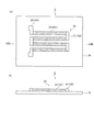
- FIG. 9 is a view for explaining an example of the magnetic sensor 4 to which the fourth embodiment is applied.
- 9 (a) is a plan view
- FIG. 9 (b) is a cross-sectional view taken along the line IXB-IXB of FIG. 9 (a).
- the magnetic sensor 4 to which the fourth embodiment is applied is opposed to the thin film magnet 40 formed of a hard magnetic material (hard magnetic material layer 105) and the thin film magnet 40.
- a magnetic sensor main body 20 configured of a soft magnetic material (soft magnetic material layer 101) to sense a magnetic field (external magnetic field).
- the magnetic sensor main body 20 includes the sensing unit 21, the connection conductor 31, and the terminal conductor 32.
- the magnetic sensor main body 20 may be similar to the magnetic sensor 1 to which the first embodiment is applied.
- the magnetic sensor 4 includes a control layer 104 that controls the magnetic anisotropy of the thin film magnet 40 to appear in the in-plane direction.
- the control layer 104 is provided on the thin film magnet 40 on the side opposite to the side on which the sensing unit 21 is provided.
- the magnetic sensor main body 20 is the same as the magnetic sensor 2 to which the second embodiment is applied, so the description will be omitted.
- the magnetic sensor 4 is sensitive to magnetic flux generated from the N pole and S pole of the thin film magnet 40 from the N pole of the thin film magnet 40 so as to pass through the sensing portion 21 in the longitudinal direction.
- a yoke 50a for inducing magnetic flux to one longitudinal end of the portion 21 and a yoke 50b for inducing magnetic flux to the S pole of the thin film magnet 40 from the other longitudinal end of the sensing portion 21 are provided.
- the yokes 50a and 50b are made of a soft magnetic material that easily transmits magnetic flux.
- the yoke 50 is composed of the soft magnetic material layer 101 that constitutes the sensing unit 21.
- the thin film magnet 40 applies a bias magnetic field to the sensing unit 21.
- the magnetic sensor 4 is configured such that the adhesion layer 103, the control layer 104, the thin film magnet 40 (hard magnetic layer 105), the insulating layer 106, and the magnetic sensor main body 20 are arranged (stacked) in this order on the nonmagnetic substrate 10. It is done.
- the adhesion layer 103, the control layer 104, the thin film magnet 40 (hard magnetic layer 105), and the insulating layer 106 are processed such that at least two opposing side surfaces are exposed.
- at least two side surfaces to be exposed are set such that two side surfaces of the hard magnetic layer 105 constituting the exposed thin film magnet 40 become an N pole and an S pole.
- the yokes 50a and 50b are provided in contact with the N pole and the S pole of the exposed thin film magnet 40, respectively, and induce the generated magnetic flux to pass through the sensing portion 21 in the longitudinal direction.
- the yokes 50a and 50b may not be provided in contact with the N pole and the S pole of the exposed thin film magnet 40, and may have a gap (gap). When the yokes 50a and 50b are in contact with the exposed N pole and S pole of the thin film magnet 40, leakage of the magnetic flux is suppressed.
- the yoke 50 (yokes 50 a and 50 b) is configured such that the shape as viewed from the upper side of the substrate 10 becomes narrower as it approaches the sensing unit 21. This is to concentrate the magnetic flux generated by the thin film magnet 40 on the sensing portion 21 (increase the magnetic flux density). That is, the width of the N pole and the S pole of the thin film magnet 40 is made wider than the width of the portion where the plurality of sensing portions 21 are provided, so that the bias magnetic field to the sensing portion 21 becomes stronger. Therefore, the width of the portion of the yoke 50 (yokes 50a and 50b) facing the sensing portion 21 may be set wider than the width of the portion where the plurality of sensing portions 21 are provided. The width of the portion of the yoke 50 (yokes 50a and 50b) facing the sensing portion 21 may not be narrowed.
- the distance between the yoke 50 (yokes 50a and 50b) and the longitudinal end of the sensing unit 21 may be, for example, 1 ⁇ m to 100 ⁇ m.
- the adhesion layer 103 improves the adhesion of the control layer 104 to the substrate 10.
- an alloy containing Cr or Ni is preferably used as the adhesion layer 103.
- the alloy containing Cr or Ni include CrTi, CrTa, NiTa and the like.
- the thickness of the adhesion layer 103 is, for example, 5 nm to 50 nm. If there is no problem in the adhesion of the control layer 104 to the substrate 10, it is not necessary to provide the adhesion layer 103.
- the control layer 104 is a layer that controls so that the magnetic anisotropy of the thin film magnet 40 formed of the hard magnetic layer 105 is expressed in the in-plane direction of the film.
- the control layer 104 it is preferable to use Cr, Mo or W or an alloy containing them (hereinafter referred to as an alloy containing Cr or the like which constitutes the control layer 104).
- CrTi, CrMo, CrV, CrW, etc. may be mentioned as an alloy containing Cr, etc., which constitutes the control layer 104.
- the thickness of the control layer 104 is, for example, 5 nm to 100 nm.
- the hard magnetic material (hard magnetic material layer 105) constituting the thin film magnet 40 is mainly composed of Co, and an alloy containing either one or both of Cr and Pt (hereinafter referred to as a Co alloy constituting the thin film magnet 40) It is good to use Examples of the Co alloy constituting the thin film magnet 40 include CoCrPt, CoCrTa, CoNiCr, CoCrPtB and the like. In addition, Fe may be contained.
- the thickness of the hard magnetic material (hard magnetic material layer 105) constituting the thin film magnet 40 is, for example, 50 nm to 500 nm.
- An alloy containing Cr or the like constituting the control layer 104 has a bcc (body-centered cubic (body centered cubic)) structure. Therefore, the hard magnetic material (hard magnetic material layer 105) constituting the thin film magnet 40 is hcp (hexagonal close-packed (hexagonal), which is easy to be crystal-grown on the control layer 104 made of an alloy containing Cr and the like of bcc structure. Close-packing)) is preferable.
- the hard magnetic layer 105 of the hcp structure is crystal-grown on the bcc structure, the c-axis of the hcp structure tends to be oriented in the plane.
- the thin film magnet 40 formed of the hard magnetic layer 105 tends to have magnetic anisotropy in the in-plane direction.
- the hard magnetic layer 105 is polycrystalline, and each crystal has magnetic anisotropy in the in-plane direction.
- this magnetic anisotropy may be referred to as magnetocrystalline anisotropy.
- the substrate 10 may be heated to 100 ° C. to 600 ° C. in order to promote crystal growth of the alloy containing Cr or the like that constitutes the control layer 104 and the Co alloy that constitutes the thin film magnet 40.
- an alloy containing Cr or the like constituting the control layer 104 is crystal-grown, and the hard magnetic layer 105 having the hcp structure is easily crystal-oriented so as to have an easy axis of magnetization in the plane. That is, the magnetic anisotropy is easily imparted to the surface of the hard magnetic layer 105.
- the insulating layer 106 is made of a nonmagnetic insulator, and electrically insulates between the thin film magnet 40 and the magnetic sensor main body 20.
- Examples of the insulator forming the insulating layer 106 include oxides such as SiO 2 and Al 2 O 3 , and nitrides such as Si 2 N 4 and AlN.
- the thickness of the insulating layer 106 is, for example, 100 nm to 500 nm.
- the yokes 50 may be made of a soft magnetic material having high permeability.
- the yoke 50 is composed of the soft magnetic material layer 101 that constitutes the sensing unit 21 of the magnetic sensor main body 20.
- the yoke 50 reduces the leakage of the magnetic flux from the thin film magnet 40, and the bias magnetic field is efficiently applied to the sensing unit 21.
- the thin film magnet 40 it is not necessary to apply a bias magnetic field from the outside by a coil or the like. Therefore, power saving and miniaturization of the magnetic sensor 4 can be achieved.
- the thin film magnet 40 may be provided as a plurality of thin film magnet pieces in the same manner as the sensing unit 21, and the thin film magnet pieces may be provided corresponding to the respective sensing units 21. That is, the sensing unit 21 may be stacked on the thin film magnet piece via the insulating layer 106. By doing this, the demagnetizing field generated inside the thin film magnet 40 becomes small, and the magnetic flux generation efficiency from the thin film magnet 40 becomes high.
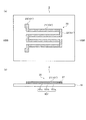
- FIG. 10 is a diagram for explaining an example of a method of manufacturing the magnetic sensor 4 to which the fourth embodiment is applied.
- 10 (a) to 10 (g) show steps in the method of manufacturing the magnetic sensor 4.
- FIG. 10 (a) to 10 (g) are representative steps and proceed in the order of FIGS. 10 (a) to 10 (g).
- 10 (a) to 10 (g) correspond to the cross-sectional view of FIG. 9 (b).
- the substrate 10 is a substrate made of a nonmagnetic material, and is, for example, an oxide substrate such as glass or sapphire, or a semiconductor substrate such as silicon.
- the substrate 10 may be provided with streak-like grooves or streak-like unevenness with a radius of curvature Ra of, for example, 0.1 nm to 100 nm, using a polishing machine or the like.
- the direction of the streak-like groove or the streak-like unevenness may be provided in a direction connecting the N pole and the S pole of the thin film magnet 40 configured by the hard magnetic material layer 105. Therefore, when the magnetic sensor 4 is arranged as in the magnetic sensor 1 shown in FIGS. 4 (a) and 4 (b) or 6 (a) and 6 (b), concentric streaks or streaks are formed. It is preferable to form asperities.
- the magnetization easy axis of the thin film magnet 40 formed of the hard magnetic layer 105 can be more easily oriented in the groove direction (direction connecting the N pole and the S pole of the thin film magnet 40). That is, the magnetization of the thin film magnet 40 is made easier.
- a lift off method is mainly used. Note that an etching method may be used.
- a resist pattern 202 having an opening at a portion where the thin film magnet 40 is to be formed is formed on the surface of the substrate 10 by known photolithography.
- the direction of the magnetic sensor 4 is set such that the direction of the magnetic field of the magnetron sputtering apparatus 300 (see FIG. 3) used in FIG. 10E is the short direction of the sensing portion 21 of the magnetic sensor main body 20 There is.
- the adhesion layer 103, the control layer 104, and the hard magnetic material layer 105 constituting the thin film magnet 40 are sequentially formed.
- a layer (film) of an alloy containing Cr or Ni to be the adhesion layer 103, a layer (film) of an alloy containing Cr or the like to be the control layer 104, and Co to be the hard magnetic layer 105 The layers (films) of the alloy are sequentially formed (deposited) sequentially.
- the substrate 10 may be heated to, for example, 100 to 600 ° C. in order to promote crystal growth.
- the substrate 10 may or may not be heated. In order to remove moisture and the like adsorbed to the substrate 10, the substrate 10 may be heated before the adhesion layer 103 is formed.
- a layer (film) such as an oxide such as SiO 2 or Al 2 O 3 or a nitride such as Si 2 N 4 or AlN to be the insulating layer 106 is formed (deposited).
- the insulating layer 106 can be formed by plasma CVD, reactive sputtering, or the like.
- the resist pattern 202 is removed, and the portions deposited on the resist pattern 202 of the adhesion layer 103, the control layer 104, the hard magnetic layer 105, and the insulating layer 106 are removed (see FIG. Lift off).
- the adhesion layer 103, the control layer 104, the hard magnetic layer 105, and the insulating layer 106 are formed on the substrate 10.
- the hard magnetic layer 105 becomes the thin film magnet 40.
- the pattern 203 is formed.
- a film of a Co alloy to be the soft magnetic layer 101 constituting the sensing unit 21 and the yoke 50 is deposited (deposited) Do.
- the magnetron sputtering apparatus 300 shown in FIG. 3 is used.
- the portion deposited on the resist pattern 203 of the soft magnetic layer 101 is removed.
- the soft magnetic material layer 101 stacked on the thin film magnet 40 (hard magnetic material layer 105) with the insulating layer 106 interposed therebetween becomes the sensing unit 21 of the magnetic sensor main body 20.
- the soft magnetic material layer 101 which is extended so that a part is in contact with the N pole or the S pole of the thin film magnet 40 and the other part is opposed to the sensing part 21 becomes a yoke 50 (yokes 50a, 50b). That is, the sensing portion 21 of the magnetic sensor main body 20 and the yoke 50 are formed by forming the soft magnetic layer 101 once.
- connection conductor 31 and the terminal conductor 32 that connect the sensing unit 21 in a zigzag manner are formed of the conductor layer 102.
- the hard magnetic layer 105 constituting the thin film magnet 40 is magnetized.
- the magnetization of the hard magnetic layer 105 is performed by applying a magnetic field larger than the coercive force of the hard magnetic layer 105 in a static magnetic field or in a pulsed magnetic field until the magnetization of the hard magnetic layer 105 is saturated (applied). .
- the magnetized hard magnetic material layer 105 becomes a thin film magnet 40, and the magnetic flux from the thin film magnet 40 passes a yoke 50 to supply a bias magnetic field to the sensing portion 21 of the magnetic sensor main body 20.
- the magnetic sensor 4 is manufactured.
- control layer 104 In the case where the control layer 104 is not provided, after forming the hard magnetic layer 105, it is necessary to provide crystal anisotropy by heating at 800 ° C. or more to cause crystal growth. . However, in the magnetic sensor 4 to which the fourth embodiment is applied, crystal growth is promoted by the control layer 104, so crystal growth by heating at 800 ° C. or more is not required.
- the magnetron sputtering apparatus 300 for forming (depositing) the soft magnetic material layer 101, the deposition rate of the soft magnetic material layer 101 is improved, and the time required for deposition (film formation) is shortened. Uniaxial magnetic anisotropy is given simultaneously with the deposition of the magnetic layer 101. Therefore, in the manufacture of the magnetic sensor 4, the step of heat treatment in a magnetic field for providing uniaxial magnetic anisotropy is unnecessary, and the steps required for the manufacture are simplified.
- the sensing portion 21 of the magnetic sensor main body 20 of the magnetic sensor 4 described in the fourth embodiment is a demagnetizing field as in the third embodiment. It is comprised by two soft-magnetic body layers provided on both sides of the suppression layer.
- portions different from the magnetic sensor 4 to which the fourth embodiment is applied will be mainly described, and the same portions will be denoted by the same reference numerals and descriptions thereof will be omitted.
- FIG. 11 is a view for explaining an example of the magnetic sensor 5 to which the fifth embodiment is applied.
- 11 (a) is a plan view
- FIG. 11 (b) is a cross-sectional view taken along line XIB-XIB of FIG. 11 (a).
- the magnetic material layer 101 'constituting the sensing portion 21 of the magnetic sensor main body 20 is a lower soft magnetic material layer. 101a, a demagnetizing field suppression layer 101b, and an upper soft magnetic layer 101c.
- the yokes 50 are formed of the soft magnetic layer 107.
- the magnetic sensor 5 is manufactured by changing the manufacturing method of the magnetic sensor 4 shown in FIG. That is, in FIG. 10E, instead of the soft magnetic layer 101, a magnetic layer 101 'composed of the lower soft magnetic layer 101a, the demagnetizing field suppression layer 101b, and the upper soft magnetic layer 101c is deposited. At this time, in the resist pattern 203, only the sensing unit 21 is open. Then, after FIG. 10F, a resist pattern in which the yokes 50 (yokes 50a and 50b) are opened is formed, and the soft magnetic layer 107 is deposited. Then, the yokes 50a and 50b may be formed by removing (lifting off) the soft magnetic layer 107 on the resist pattern as well as the resist pattern.
- two sensing units 21 of the magnetic sensor main body 20 are provided on both sides of the demagnetizing field suppression layer as in the magnetic sensor 5 of the fifth embodiment. It is composed of a soft magnetic layer. Furthermore, the yoke 50 is also composed of two soft magnetic layers provided with the demagnetizing field suppression layer interposed therebetween.
- portions different from the magnetic sensor 5 according to the fifth embodiment will be mainly described, and the same portions are denoted with the same reference numerals and description thereof will be omitted.
- FIG. 12 is a view for explaining an example of the magnetic sensor 6 to which the sixth embodiment is applied.
- 12 (a) is a plan view
- FIG. 12 (b) is a cross-sectional view taken along line XIIB-XIIB of FIG. 12 (a).
- the magnetic sensor 6 to which the sixth embodiment is applied is different in the yoke 50 (yokes 50a and 50b).
- the yoke 50 (yokes 50a and 50b) is the same as the magnetic sensor 21 of the magnetic sensor main body 20 of the magnetic sensor 5 to which the fifth embodiment is applied. It is composed of a body layer 101 '. That is, the yoke 50 (yokes 50a and 50b) includes the lower soft magnetic layer 101a, the demagnetizing field suppression layer 101b, and the upper soft magnetic layer 101c.
- the magnetic field suppression layer 101b and the upper soft magnetic layer 101c may be formed (deposited) in order.
Landscapes
- Engineering & Computer Science (AREA)
- Chemical & Material Sciences (AREA)
- Physics & Mathematics (AREA)
- Power Engineering (AREA)
- General Physics & Mathematics (AREA)
- Condensed Matter Physics & Semiconductors (AREA)
- Materials Engineering (AREA)
- Manufacturing & Machinery (AREA)
- Organic Chemistry (AREA)
- Metallurgy (AREA)
- Mechanical Engineering (AREA)
- Chemical Kinetics & Catalysis (AREA)
- Hall/Mr Elements (AREA)
- Measuring Magnetic Variables (AREA)
- Physical Vapour Deposition (AREA)
Abstract
磁気センサの製造方法は、マグネトロンスパッタリングにより、基板10上に磁界を感受する感受部21を構成する軟磁性体層101を堆積する軟磁性体層堆積工程と、軟磁性体層101のマグネトロンスパッタリングに用いた磁界により一軸磁気異方性が付与された部分に、磁界を感受する感受部21を形成する感受部形成工程とを含む。
Description
本発明は、磁気センサの製造方法及び磁気センサ集合体に関する。
公報記載の従来技術として、磁気インピーダンス効果を利用した磁気検出素子であって、非磁性基板上に高透磁率磁性膜を形成して構成され、前記高透磁率磁性膜は、磁界検出方向に沿った複数本の直線部分が所定間隔で平行に並び、順次折り返すように連結され、電気的に直列接続されたつづら折り状パターンに形成され、且つ磁化容易軸方向が磁界検出方向に対し膜面内で垂直な方向になるように磁気異方性が付けられており、該高透磁率磁性膜の両端部から高周波電流を印加し外部磁界により前記両端部間に発生するインピーダンスの変化を電気信号に変換して出力を得られるようにした磁気検出素子が存在する(特許文献1参照)。
ところで、磁気インピーダンス効果を用いた磁気センサでは、短手方向に一軸異方性が付与された短冊状の軟磁性体が感受部として用いられる。そして、軟磁性体の一軸異方性は、感受部が形成された後に、磁界中熱処理などにより付与されていた。
本発明は、磁界中熱処理を用いる場合に比べて、製造に要する工程が簡略化された磁気センサの製造方法などを提供する。
本発明は、磁界中熱処理を用いる場合に比べて、製造に要する工程が簡略化された磁気センサの製造方法などを提供する。
本発明が適用される磁気センサの製造方法は、マグネトロンスパッタリングにより、基板上に磁界を感受する感受部を構成する軟磁性体層を堆積する軟磁性体層堆積工程と、軟磁性体層のマグネトロンスパッタリングに用いた磁界により一軸磁気異方性が付与された部分に、磁界を感受する感受部を形成する感受部形成工程とを含む。
このような磁気センサの製造方法の感受部形成工程において、長手方向と短手方向とを有する感受部の短手方向が一軸磁気異方性の方向を向くように感受部を形成することを特徴とすることができる。
また、マグネトロンスパッタリングは、基板の表面に対向する面内において、磁界を形成する磁石が回転するカソードを用いて行うことを特徴とすることができる。
さらに、このような磁気センサの製造方法において、感受部の一軸磁気異方性の方向と交差する方向に磁界を形成する、硬磁性体で構成された薄膜磁石が設けられた基板に対して、軟磁性体層堆積工程と、感受部形成工程とが行われることを特徴とすることができる。
このような磁気センサの製造方法の感受部形成工程において、長手方向と短手方向とを有する感受部の短手方向が一軸磁気異方性の方向を向くように感受部を形成することを特徴とすることができる。
また、マグネトロンスパッタリングは、基板の表面に対向する面内において、磁界を形成する磁石が回転するカソードを用いて行うことを特徴とすることができる。
さらに、このような磁気センサの製造方法において、感受部の一軸磁気異方性の方向と交差する方向に磁界を形成する、硬磁性体で構成された薄膜磁石が設けられた基板に対して、軟磁性体層堆積工程と、感受部形成工程とが行われることを特徴とすることができる。
他の観点から捉えると、本発明が適用される磁気センサ集合体は、磁界を感受する感受部が、感受部を構成する軟磁性体層の形成に用いられたマグネトロンスパッタリングにおいて形成された磁界の位置を反映して、それぞれが配置された複数の磁気センサを備える。
このような磁気センサ集合体における複数の磁気センサのそれぞれの感受部は、長手方向と短手方向とを有し、短手方向がマグネトロンスパッタリングにおいて形成された磁界の方向を向いていることを特徴とすることができる。
さらに、複数の磁気センサのそれぞれは、感受部の一軸磁気異方性の方向と交差する方向に磁界を形成する、硬磁性体で構成された薄膜磁石を備えることを特徴とすることができる。
このような磁気センサ集合体における複数の磁気センサのそれぞれの感受部は、長手方向と短手方向とを有し、短手方向がマグネトロンスパッタリングにおいて形成された磁界の方向を向いていることを特徴とすることができる。
さらに、複数の磁気センサのそれぞれは、感受部の一軸磁気異方性の方向と交差する方向に磁界を形成する、硬磁性体で構成された薄膜磁石を備えることを特徴とすることができる。
本発明によれば、磁界中熱処理を用いる場合に比べて、製造に要する工程が簡略化された磁気センサの製造方法などが提供できる。
本明細書で説明する磁気センサは、いわゆる磁気インピーダンス効果素子を用いたものである。
以下、添付図面を参照して、本発明の実施の形態について詳細に説明する。
以下、添付図面を参照して、本発明の実施の形態について詳細に説明する。
[第1の実施の形態]
(磁気センサ1の構成)
まず、第1の実施の形態が適用される磁気センサ1の構成を説明する。
図1は、第1の実施の形態が適用される磁気センサ1の一例を説明する図である。図1(a)は、平面図、図1(b)は、図1(a)のIB-IB線での断面図である。
図1(a)、(b)に示すように、磁気センサ1は、基板10と、基板10上に設けられ、軟磁性体(後述する軟磁性体層101)で構成された磁気センサ本体20とを備える。
図1(a)に示すように、磁気センサ本体20は、磁界(外部磁界)の変化を感知する複数の感受部21と、複数の感受部21を直列(つづら折り)接続する接続部22と、感受部21に電流を供給する電線が接続される端子部23とを備える。なお、本明細書においては、感受部21を構成する軟磁性体層101を( )内に表記する。他の場合も同様である。
ここで軟磁性体とは、外部磁界によって容易に磁化されるが、外部磁界を取り除くと速やかに磁化のないか又は小さい元の状態に戻る、いわゆる保磁力の小さい材料である。軟磁性体としては、例えば、Coを主成分にした合金(以下では、感受部21を構成するCo合金と表記する。)に高融点金属Nb、Ta、W等を添加したアモルファス合金が用いうる。感受部21を構成するCo合金としては、CoNbZr、CoFeTa、CoWZr等が挙げられる。なお、本明細書においては、合金の組成比は、特に示していない。以下同様である。
基板10は、非磁性体からなる基板であって、例えば、ガラス、サファイア等の酸化物基板や、シリコン等の半導体基板が用いうる。ここでは、基板10は、ガラスであるとして説明する。なお、基板10は、一例として直径が約95mmの円盤状であって、厚さは約0.5mmである。そして、複数の磁気センサ1が基板10上に一括して製造されたのち、個々の磁気センサ1に分割される(切り出される)。図1は、切り出された1個の磁気センサ1である。
なお、基板10が導電体である場合には、基板10上に電気的な絶縁層を設けておけばよい。
なお、基板10が導電体である場合には、基板10上に電気的な絶縁層を設けておけばよい。
次に、磁気センサ本体20を説明する。
感受部21は、後述する軟磁性体層101で構成された、長手方向に電流が流れるように設けられた短冊状の部材である。そして、複数の感受部21(ここでは、4個)が、長手方向が平行に配置(配列)されている。なお、感受部21は1個でもよい。
感受部21は、後述する軟磁性体層101で構成された、長手方向に電流が流れるように設けられた短冊状の部材である。そして、複数の感受部21(ここでは、4個)が、長手方向が平行に配置(配列)されている。なお、感受部21は1個でもよい。
そして、接続部22は、軟磁性体層101で構成され、隣接する感受部21の端部間に設けられている。そして、接続部22は、複数の感受部21を直列(つづら折り)に接続する。ここでは、感受部21が4個あるため、接続部22は3個である。感受部21が2個である場合には、接続部22は1個でよい。なお、感受部21が1個である場合には、接続部22を備えなくともよい。接続部22の幅は、感受部21と同様であればよい。
さらに、端子部23は、軟磁性体層101で構成され、接続部22で接続されていない感受部21の端部(2個)にそれぞれ設けられている。端子部23は、感受部21から引き出す引き出し部分と、電流を供給する電線を接続する部分(パッド)とを備える。なお、電線を接続する部分は、電線を接続しうる大きさであればよい。
図1(a)、(b)に示すように、感受部21、接続部22及び端子部23は、同一の軟磁性体層101を加工して形成されていて、連続している。
磁気センサ1は、感受部21の長手方向と交差する短手方向(幅方向)に磁化容易軸が向いた、一軸磁気異方性が付与されている。
使用時には、外部から感受部21の長手方向に磁束が透過するように、例えばコイルに電流を流して発生させたバイアス磁界が印加される。そして、バイアス磁界が印加された状態で、2個の端子部23から感受部21に高周波電流を流して、端子部23間の抵抗値(インピーダンス)を計測する。端子部23間の抵抗値(インピーダンス)は、外部磁界の感受部21の長手方向に沿った方向の成分を感受する。よって、端子部23間の抵抗値(インピーダンス)の計測から、外部磁界又は外部磁界の変化が測定される。
使用時には、外部から感受部21の長手方向に磁束が透過するように、例えばコイルに電流を流して発生させたバイアス磁界が印加される。そして、バイアス磁界が印加された状態で、2個の端子部23から感受部21に高周波電流を流して、端子部23間の抵抗値(インピーダンス)を計測する。端子部23間の抵抗値(インピーダンス)は、外部磁界の感受部21の長手方向に沿った方向の成分を感受する。よって、端子部23間の抵抗値(インピーダンス)の計測から、外部磁界又は外部磁界の変化が測定される。
なお、バイアス磁界は、外部磁界の変化に対して、端子部23間の抵抗値(インピーダンス)変化が大きい状態に設定する。つまり、バイアス磁界を印加して、外部磁界に対してインピーダンス変化の急峻なところを使うと、微弱な外部磁界の変化を捉えることが可能となる。
感受部21は、例えば短手方向の幅が数10μm、長手方向の長さが約1mm、厚さが0.5μm~5μmである。そして、平行して配置(配列)される2個の感受部21の間隔は、50~100μmである。よって、磁気センサ1の平面形状は、数mm角である。
なお、計測する外部磁界の値や用いる軟磁性体材料などによって、他の値を用いてもよい。
なお、計測する外部磁界の値や用いる軟磁性体材料などによって、他の値を用いてもよい。
(磁気センサ1の製造方法)
次に、磁気センサ1の製造方法を説明する。複数の磁気センサ1が一括して製造される。ここでは、1個の磁気センサ1に着目して説明する。以下で説明する製造方法では、リフトオフ法を用いる。なお、エッチング法を用いてもよい。
図2は、磁気センサ1の製造方法の一例を説明する図である。図2(a)~(c)は、磁気センサ1の製造方法における工程を示す。なお、図2(a)~(c)は、代表的な工程であって、図2(a)~(c)の順に進む。図2(a)~(c)は、図1(b)の断面図に対応する。
次に、磁気センサ1の製造方法を説明する。複数の磁気センサ1が一括して製造される。ここでは、1個の磁気センサ1に着目して説明する。以下で説明する製造方法では、リフトオフ法を用いる。なお、エッチング法を用いてもよい。
図2は、磁気センサ1の製造方法の一例を説明する図である。図2(a)~(c)は、磁気センサ1の製造方法における工程を示す。なお、図2(a)~(c)は、代表的な工程であって、図2(a)~(c)の順に進む。図2(a)~(c)は、図1(b)の断面図に対応する。
図2(a)は、レジストパターン形成工程であって、次の図2(b)で堆積する軟磁性体層101をリフトオフするためのレジストパターン201を基板10上に形成する。
ここでは、基板10を洗浄した後、基板10の一方の面(以下、表面と表記する。)上に、磁気センサ本体20が形成される部分を開口部とするレジストパターン201を、公知のフォトリソグラフィにより形成する。
ここでは、基板10を洗浄した後、基板10の一方の面(以下、表面と表記する。)上に、磁気センサ本体20が形成される部分を開口部とするレジストパターン201を、公知のフォトリソグラフィにより形成する。
なお、レジストパターン201は、磁気センサ本体20の感受部21が、後述するマグネトロン方式のスパッタリング装置300(マグネトロンスパッタリング装置300)で用いられる磁界内に配置され、且つ、感受部21の短手方向(幅方向)が磁界の方向に向くように形成されている。
ここで、短手方向(幅方向)が磁界の方向を向くとは、磁界の方向と短手方向とのなす角度が45°未満であることをいう。なお、磁界の方向と短手方向とのなす角度は、より小さいほどよい。
ここで、短手方向(幅方向)が磁界の方向を向くとは、磁界の方向と短手方向とのなす角度が45°未満であることをいう。なお、磁界の方向と短手方向とのなす角度は、より小さいほどよい。
図2(b)は、軟磁性体層堆積工程であって、レジストパターン201が形成された基板10の表面上に軟磁性体の層(軟磁性体層101)を堆積する。
ここでは、軟磁性体層101は、マグネトロンスパッタリング装置300により、軟磁性体で構成されたターゲット(後述する図3に示すターゲット)を用いて、基板10上に堆積される。なお、軟磁性体は、前述した感受部21を構成するCo合金である。
なお、マグネトロンスパッタリング装置300により軟磁性体層101など堆積することを、マグネトロンスパッタリングにより軟磁性体層101などを堆積すると表記することがある。
ここでは、軟磁性体層101は、マグネトロンスパッタリング装置300により、軟磁性体で構成されたターゲット(後述する図3に示すターゲット)を用いて、基板10上に堆積される。なお、軟磁性体は、前述した感受部21を構成するCo合金である。
なお、マグネトロンスパッタリング装置300により軟磁性体層101など堆積することを、マグネトロンスパッタリングにより軟磁性体層101などを堆積すると表記することがある。
図2(c)は、軟磁性体層リフトオフ工程であって、基板10上に堆積された軟磁性体層101が、リフトオフにより感受部21、接続部22及び端子部23を含む磁気センサ本体20に加工される。
ここでは、レジストパターン201を除去することで、レジストパターン201上に堆積した軟磁性体層101が除去される。これにより、レジストパターン201の開口部に軟磁性体層101が残る。このようにして、磁気センサ本体20が形成される。
なお、この軟磁性体層リフトオフ工程は、感受部形成工程の一例である。エッチング法を用いる場合には、エッチングにより感受部21を形成する工程が感受部形成工程となる。
ここでは、レジストパターン201を除去することで、レジストパターン201上に堆積した軟磁性体層101が除去される。これにより、レジストパターン201の開口部に軟磁性体層101が残る。このようにして、磁気センサ本体20が形成される。
なお、この軟磁性体層リフトオフ工程は、感受部形成工程の一例である。エッチング法を用いる場合には、エッチングにより感受部21を形成する工程が感受部形成工程となる。
ここでは、磁気センサ本体20の感受部21がマグネトロンスパッタリング装置300の磁界内にあり、且つ、感受部21の短手方向(幅方向)が、マグネトロンスパッタリング装置300の磁界の方向に向くように設定されている。よって、軟磁性体層101は、成膜(堆積)中に、感受部21の短手方向(幅方向)に磁化容易軸が向いた一軸磁気異方性が付与される。つまり、一軸磁気異方性は、マグネトロンスパッタリング装置300の磁界によって誘導されて付与される。よって、この一軸磁気異方性は、誘導磁気異方性と表記されることがある。これにより、磁気センサ1が形成された後に、磁界中熱処理を行うことを要しない。
なお、磁界中熱処理は、例えば3kG(0.3T)の回転磁界中における400℃での熱処理と、それに引き続く3kG(0.3T)の静磁界中における400℃での熱処理である。
つまり、第1の実施の形態が適用される磁気センサ1の製造方法では、400℃などの高温での磁界中熱処理を要しない。
つまり、第1の実施の形態が適用される磁気センサ1の製造方法では、400℃などの高温での磁界中熱処理を要しない。
(マグネトロンスパッタリング装置300)
ここで、図2(b)におけるマグネトロンスパッタリング装置300を用いた軟磁性体層101の形成について説明する。まず、マグネトロンスパッタリング装置300を説明する。
図3は、マグネトロンスパッタリング装置300の概要を説明する断面図である。ここでのマグネトロンスパッタリング装置300は、図3のO-O線を回転の軸とする円筒状である。
マグネトロンスパッタリング装置300は、隔壁310とマグネトロンカソード320とを備える。隔壁310とマグネトロンカソード320とは、ポリテトラフルオロエチレンなどの絶縁部材311を介して、密閉された空間であるチャンバ340を構成する。
チャンバ340内には、基板10を保持する基板ホルダ350を備える。
隔壁310は、接地(GND)されている。基板ホルダ350は、隔壁310を介して接地(GND)されアノードとして機能する。つまり、接地された基板ホルダ350とマグネトロンカソード320との間に、高周波電源360が接続されている。なお、高周波電源360の代わりに、直流電源が接続され、基板ホルダ350とマグネトロンカソード320との間に、直流(DC)が印加されるようにしてもよい。
なお、図3では図示していないが、マグネトロンスパッタリング装置300には、上記の他にチャンバ340内を減圧する真空ポンプ、チャンバ340内にスパッタリングに用いるガス、例えばArなどを導入するガス供給機構やチャンバ340内の圧力を予め定められた値に保持する圧力調整機構を備える。また、マグネトロンカソード320を冷却するために、マグネトロンカソード320に冷却液を供給する冷却機構を備えてもよい。そして、基板10を加熱するための加熱機構、例えば赤外線ランプや、逆に、基板10を冷却するために、基板ホルダ350に冷却液を供給する冷却機構を備えてもよい。
マグネトロンカソード320は、カソード筐体321、基板10上に形成する薄膜の材料であるターゲット322、ターゲット322を保持するバッキングプレート323、及び、バッキングプレート323を透過して磁界をターゲット322側に生じさせる磁気回路330を備える。
ターゲット322は、前述した感受部21を構成するCo合金で構成されている。
バッキングプレート323は、導電率の高い無酸素銅などで構成されている。そして、表面に、ターゲット322が導電性の接着剤などで固定されている。
カソード筐体321は、ステンレス鋼などで構成されている。カソード筐体321にターゲット322が取り付けられたバッキングプレート323が固定され、バッキングプレート323のターゲット322の設けられていない側に、磁気回路330が設けられている。
ターゲット322の大きさ(直径)は、基板10の予め定められた領域(範囲)に膜が形成(堆積)されるように設定されている。ここでは、ターゲット322の直径は、基板10の直径より大きくしている。
バッキングプレート323は、導電率の高い無酸素銅などで構成されている。そして、表面に、ターゲット322が導電性の接着剤などで固定されている。
カソード筐体321は、ステンレス鋼などで構成されている。カソード筐体321にターゲット322が取り付けられたバッキングプレート323が固定され、バッキングプレート323のターゲット322の設けられていない側に、磁気回路330が設けられている。
ターゲット322の大きさ(直径)は、基板10の予め定められた領域(範囲)に膜が形成(堆積)されるように設定されている。ここでは、ターゲット322の直径は、基板10の直径より大きくしている。
磁気回路330は、バッキングプレート323側にN極が露出した磁石(マグネット)331と、S極が露出した磁石332と、磁石331、332のバッキングプレート323側とは反対側に設けられ、磁石332のN極からの磁束を磁石331のS極に誘導するヨーク333を備える。磁石331、332には、一般に永久磁石が用いられる。
ここでは、後述する図4に示すように、磁石331、332は、バッキングプレート323側にN極が露出した磁石331が外側、S極が露出した磁石332が内側になるように同心円状に設けられている。
ここでは、後述する図4に示すように、磁石331、332は、バッキングプレート323側にN極が露出した磁石331が外側、S極が露出した磁石332が内側になるように同心円状に設けられている。
すると、磁石331のN極から磁石332のS極に向かう磁力線(矢印で示す)が、バッキングプレート323及びターゲット322を貫いて、チャンバ340内に発生する。そして、この磁力線の一部は、基板ホルダ350に保持された基板10に到達し、基板10を、表面に平行な方向に通過する。つまり、基板10には、磁力線が通過する部分において、表面に平行な方向の磁界が発生する。
すなわち、基板10に発生する表面に平行な方向の磁界により、基板10上に堆積(形成)される軟磁性体層101の堆積に伴って一軸磁気異方性が付与される。
すなわち、基板10に発生する表面に平行な方向の磁界により、基板10上に堆積(形成)される軟磁性体層101の堆積に伴って一軸磁気異方性が付与される。
なお、マグネトロンスパッタリング装置300では、高周波電源360によって発生させた放電によって発生した電子を、ターゲット322の表面の磁力線によって、ターゲット322の近傍に集中させる(閉じ込める)。これにより、電子とガスとの衝突確率を増加させてガスの電離を促進し、膜の堆積速度(成膜速度)を向上させている。なお、磁力線によって電子を集中させたターゲット322の表面が、電離したガスのイオンの衝撃で浸食(エロージョン)される範囲となる。
基板ホルダ350は、ステンレス鋼などで構成されている。そして、基板ホルダ350は、基板10を保持する機構(不図示)により、基板10を保持する。
前述したように、マグネトロンスパッタリング装置300は、円筒状である。そして、ターゲット322も円形(円盤状)である。そして、基板10も円形(円盤状)であって、ターゲット322に対向するように基板ホルダ350に保持されている(後述する図4参照)。
前述したように、マグネトロンスパッタリング装置300は、円筒状である。そして、ターゲット322も円形(円盤状)である。そして、基板10も円形(円盤状)であって、ターゲット322に対向するように基板ホルダ350に保持されている(後述する図4参照)。
以上説明したように、図3に示すマグネトロンスパッタリング装置300は、いわゆる基板10の一枚毎に、膜を形成(堆積)する枚葉式のスパッタリング装置である。
また、図3に示すマグネトロンスパッタリング装置300では、基板10の表面(ターゲット322の表面)を水平(図3の紙面における左右方向)に配置するように構成したが、垂直(図3の紙面における上下方向に)に配置するように構成してもよい。
また、図3に示すマグネトロンスパッタリング装置300では、基板10の表面(ターゲット322の表面)を水平(図3の紙面における左右方向)に配置するように構成したが、垂直(図3の紙面における上下方向に)に配置するように構成してもよい。
図4は、マグネトロンスパッタリング装置300における磁気回路330の構成及び基板10に形成された磁気センサ1の配置(磁気センサ集合体)を示す図である。図4(a)は、ターゲット322側から見た磁気回路330の構成、図4(b)は、基板10に形成された磁気センサ1の配置(磁気センサ集合体)を示す。
図4(a)に示すように、ターゲット322は、円形である。そして、ターゲット322を通して見た磁気回路330は、同心円状に磁石331のN極と磁石332のS極とが設けられている。そして、ターゲット322を透過して、磁石331のN極から磁石332のS極に向かう磁力線(矢印)が形成されている。
そして、図4(b)に示すように、基板10は、ターゲット322に対向して設けられた円板状である。なお、図4(b)には、対向する磁気回路330の磁石331、332の位置を合わせて示している。そして、磁気センサ1は、基板10上の磁力線が通過する部分(磁界)において、磁力線の通過する方向に軟磁性体層101で形成される感受部21の短手方向(幅方向)が向くように配置(配列)されている。例えば、磁気センサ1は、磁気回路330における磁石331のN極の作る円と磁石332のS極が作る円との内側に、感受部21の短手方向(幅方向)が円の径方向に沿うように配置(配列)されている。
ここでは、磁気回路330における磁石331のN極の作る円と磁石332のS極が作る円との間に1個の磁気センサ1を記載している。これは、磁気センサ1の感受部21と、磁石331のN極と磁石332のS極との作る磁界との関係を説明するためである。磁気センサ1は、磁気センサ本体20における感受部21の短手方向が磁界の方向に沿うように配置されている。そして、複数の磁気センサ1が、円周方向に沿って配置されている。
なお、磁気センサ1の平面形状は、前述したように数mm角である。よって、実際には、磁石331のN極と磁石332のS極とで形成される磁界の方向には、複数の磁気センサ1が配置されている。また、円周方向においても同様である。
なお、磁気センサ1の平面形状は、前述したように数mm角である。よって、実際には、磁石331のN極と磁石332のS極とで形成される磁界の方向には、複数の磁気センサ1が配置されている。また、円周方向においても同様である。
なお、基板10の中心部や外周部は、磁気回路330による磁界の影響を受けにくい。つまり、磁気回路330による磁界によって、軟磁性体層101に一軸磁気異方性が付与されにくい。基板10上の磁気センサ1を設ける領域は、予め定められた一軸磁気異方性が付与される領域であればよい。なお、磁石331のN極と磁石332のS極との間が、磁界が強い。よって、磁石331のN極と磁石332のS極との間に、磁気センサ1を配置することがよい。なお、予め定められた一軸磁気異方性が付与されるならば、磁気センサ1を配置する領域は磁石331のN極と磁石332のS極との間でなくともよい。よって、一軸磁気異方性が付与しづらい基板10の中心部や外周部には、磁気センサ1を配置しないことがよい。しかし、基板10の中心部や外周部に磁気センサ1を配置した場合には、基板10の中心部や外周部に配置された磁気センサ1には、磁界中熱処理などにより、一軸磁気異方性を付与すればよい。
そして、基板10上に複数の磁気センサ1が形成された状態を、磁気センサ集合体と表記する。磁気センサ1は、複数の磁気センサ1が形成された基板10のまま出荷されることがある。つまり、出荷先において、基板10が分割(切断)され、個々の磁気センサ1にされる。なお、基板10は、一部であってもよい。
図4(b)では、基板10から個々の磁気センサ1が切り出されていない磁気センサ集合体を示している。しかし、磁気センサ集合体は、基板10を粘着シートに貼り付け、レーザなどの切断手段により基板10を磁気センサ1毎に切断した後、磁気センサ1を取り出しやすいように粘着シートを引き延ばした状態であってもよい。磁気センサ1は、このような状態においても出荷されうる。つまり、出荷先において、粘着テープから個々の磁気センサ1が取り出される。なお、基板10は、一部であってもよい。
いずれの磁気センサ集合体においても、磁気センサ1は、軟磁性体層101を形成するマグネトロンスパッタリング装置300のマグネトロンカソード320における磁気回路330の磁石331、332の配置を反映した状態で配置されている。
以上説明したように、第1の実施の形態では、軟磁性体層101の形成(堆積)にマグネトロンスパッタリング装置300を用いることにより、軟磁性体層101の堆積速度を向上させて、堆積(成膜)に係る所要時間を短縮するとともに、軟磁性体層101の堆積と同時に一軸磁気異方性を付与している。よって、磁気センサ1の製造において、一軸磁気異方性を付与するための磁界中熱処理工程を不要にし、製造に要する工程を簡略化している。
(変形例1)
次に、マグネトロンスパッタリング装置300における磁気回路330の変形例1を説明する。
図5は、マグネトロンスパッタリング装置300における磁気回路330の変形例1と、基板10に形成された磁気センサ1の配置(磁気センサ集合体)を示す図である。図5(a)は、ターゲット322側から見た変形例1の磁気回路330の構成、図5(b)は、基板10に形成された磁気センサ1の配置(磁気センサ集合体)である。
次に、マグネトロンスパッタリング装置300における磁気回路330の変形例1を説明する。
図5は、マグネトロンスパッタリング装置300における磁気回路330の変形例1と、基板10に形成された磁気センサ1の配置(磁気センサ集合体)を示す図である。図5(a)は、ターゲット322側から見た変形例1の磁気回路330の構成、図5(b)は、基板10に形成された磁気センサ1の配置(磁気センサ集合体)である。
図5(a)に示すように、変形例1の磁気回路330におけるターゲット322の平面形状は、長方形である。つまり、変形例1の磁気回路330を備えるマグネトロンスパッタリング装置300は、チャンバ340が円筒状でなく、角柱状である。なお、他の構成は、図3に示したマグネトロンスパッタリング装置300と同様である。よって、同様の部分の説明を省略する。
そして、ターゲット322を通して見た変形例1の磁気回路330は、長方形のターゲット322の内側に、磁石331のN極が長方形の辺に沿って設けられ、磁石332のS極がその内側において、長方形の辺に沿って配置(配列)されている。
そして、ターゲット322を通して見た変形例1の磁気回路330は、長方形のターゲット322の内側に、磁石331のN極が長方形の辺に沿って設けられ、磁石332のS極がその内側において、長方形の辺に沿って配置(配列)されている。
ここでは、図5(b)に示すように、基板10は、ターゲット322に対向して設けられた長方形である。なお、図5(b)には、対向する磁気回路330の磁石331、332の位置を合わせて示している。そして、磁気センサ1は、基板10上の磁力線が通過する部分において、磁力線の通過する方向(磁界の方向)に軟磁性体層101で形成された感受部21の短手方向(幅方向)が向くように配置されている。つまり、磁気センサ1は、磁気回路330の磁石331のN極と磁石332のS極とが作る磁界の内側に、感受部21の短手方向(幅方向)が磁界の方向に沿うように設けられている。
ここでも、磁気回路330における磁石331のN極と磁石332のS極との間に1個の磁気センサ1を記載している。これは、磁気センサ1の感受部21と、磁石331のN極と磁石332のS極との作る磁界との関係を説明するためである。磁気センサ1は、磁気センサ本体20における感受部21の短手方向が磁界の方向に沿うように、磁石331、332の設けられた長方形の辺に沿って配置されている。
なお、磁気センサ1の平面形状は、前述したように数mm角である。よって、磁石331のN極と磁石332のS極との間には、複数の磁気センサ1が配置されている。また、磁石331、332の設けられた長方形の辺に沿う方向においても同様である。
なお、磁気センサ1の平面形状は、前述したように数mm角である。よって、磁石331のN極と磁石332のS極との間には、複数の磁気センサ1が配置されている。また、磁石331、332の設けられた長方形の辺に沿う方向においても同様である。
図5(b)では、基板10から個々の磁気センサ1が切り出されていない磁気センサ集合体を示している。しかし、磁気センサ集合体は、基板10を粘着シートに貼り付け、レーザなどの切断手段により基板10を磁気センサ1毎に切断した後、磁気センサ1を取り出しやすいように粘着シートを引き延ばした状態であってもよい。磁気センサ1は、このような状態においても出荷されうる。つまり、出荷先において、粘着テープから個々の磁気センサ1が取り出される。なお、基板10は、一部であってもよい。
いずれの磁気センサ集合体においても、磁気センサ1は、軟磁性体層101を形成するマグネトロンスパッタリング装置300のマグネトロンカソード320における磁気回路330の磁石331、332の配置を反映した状態で配置されている。
なお、図5(b)に示すように、基板10は、ターゲット322の平面形状に対応するように、長方形とした。しかし、基板10は、図4(b)に示すような円形であってもよい。複数の磁気センサ1が、磁気回路330の磁石331のN極と磁石332のS極との作る磁界に対応して配置されていればよい。
なお、図5(a)では、変形例1の磁気回路330を構成する磁石331、332は、長方形であるとしたが、正方形であってもよく、多角形であってもよい。そして、製造される磁気センサ1の感受部21の短手方向が磁石331、332の発生する磁界の方向に配置されていればよい。
(変形例2)
次に、マグネトロンスパッタリング装置300における磁気回路330の変形例2を説明する。
図6は、マグネトロンスパッタリング装置300における磁気回路330の変形例2の構成と、基板10に形成された磁気センサ1の配置(磁気センサ集合体)を示す図である。図6(a)は、ターゲット322側から見た変形例2の磁気回路330の構成、図6(b)は、基板10に形成された磁気センサ1の配置(磁気センサ集合体)を示す。
次に、マグネトロンスパッタリング装置300における磁気回路330の変形例2を説明する。
図6は、マグネトロンスパッタリング装置300における磁気回路330の変形例2の構成と、基板10に形成された磁気センサ1の配置(磁気センサ集合体)を示す図である。図6(a)は、ターゲット322側から見た変形例2の磁気回路330の構成、図6(b)は、基板10に形成された磁気センサ1の配置(磁気センサ集合体)を示す。
図6(a)に示すように、変形例2の磁気回路330では、図4に示した磁気回路330と同様に、ターゲット322が円盤状であって、磁石331が、磁石332を取り囲むように設けられている。しかし、磁石331は、その端がターゲット322の中心Cから、距離αの部分と、距離αより短い距離βの部分とを含むように構成されている(α>β)。そして、磁石331と磁石332との間の距離γは、大略等しく設けられている。
なお、変形例2の磁気回路330を備えるマグネトロンスパッタリング装置300の他の構成は、図3に示したマグネトロンスパッタリング装置300と同様である。よって、同様の部分の説明を省略する。
なお、変形例2の磁気回路330を備えるマグネトロンスパッタリング装置300の他の構成は、図3に示したマグネトロンスパッタリング装置300と同様である。よって、同様の部分の説明を省略する。
そして、磁石331及び磁石332は、この状態を維持して、ターゲット322の中心Cを回転軸として回転するようになっている。なお、磁石331、332を備える磁気回路330が回転し、ターゲット322(バッキングプレート323)は回転しない。つまり、磁気回路330は、ターゲット322(バッキングプレート323)の裏面において、ターゲット322(バッキングプレート323)の面に平行な仮想的な面(磁石331のN極の端部と磁石332のS極の端部とを含む面)内で回転する。ここでは、ターゲット322と基板10とは、平行に配置されているので、磁気回路330は、基板10の表面に平行な面内で回転する。なお、基板10に対して必ずしも平行な面内で回転することを要せず、基板10の表面に対向する面内で回転すればよい。
このようにすることで、ターゲット322上には、中心Cから距離αと距離α-γの部分にできる磁界と、距離βと距離β-γの部分にできる磁界とが、交互に発生する。このようにすることで、図4(a)に示した場合に比べ、電子が補足される領域(面積)が拡大する。これにより、ターゲット322がイオンの衝撃で浸食(エロージョン)される範囲が広がり、ターゲット322の使用効率が高くなる。
また、基板10上においても、磁界が形成される面積が拡大することから、軟磁性体層101に一軸磁気異方性が付与される面積が拡大する。つまり、磁気センサ1を形成しうる領域が拡大する。よって、図6(b)に示すように、磁気センサ1は、磁気回路330における磁石331、332が作る磁力線が通過する部分において、磁力線の通過する方向(磁界の方向)に軟磁性体層101で形成された感受部21の短手方向(幅方向)が向くように配置されている。例えば、磁気センサ1は、磁気回路330における磁石331、332が作る磁界の内側すなわち、中心Cから磁石331のN極までの最大距離を半径とする円と、中心Cから磁石332のS極までの最小距離を半径とする円との間に配置されている。このように、図4(b)に示した場合に比べ、基板10上に製造できる磁気センサ1の数が増加する。
なお、図6(b)には、対向する磁気回路330の磁石331、332の位置を合わせて示している。
なお、図6(b)には、対向する磁気回路330の磁石331、332の位置を合わせて示している。
ここでは、中心Cから磁石331のN極までの最大距離を半径とする円と、中心Cから磁石332のS極までの最小距離を半径とする円との間の直径方向に3個の磁気センサ1を記載している。これは、磁気センサ1の感受部21と、磁石331のN極と磁石332のS極との作る磁界との関係を説明するためである。磁気センサ1は、磁気センサ本体20における感受部21の短手方向が磁界の方向に沿うように、円周に沿って配置されている。
なお、磁気センサ1の平面形状は、前述したように数mm角である。よって、磁石331のN極と磁石332のS極とが作る磁界の方向(直径方向)には、複数の磁気センサ1が配置されている。また、円周方向においても同様である。
なお、磁気センサ1の平面形状は、前述したように数mm角である。よって、磁石331のN極と磁石332のS極とが作る磁界の方向(直径方向)には、複数の磁気センサ1が配置されている。また、円周方向においても同様である。
図6(b)では、基板10から個々の磁気センサ1が切り出されていない磁気センサ集合体を示している。しかし、磁気センサ集合体は、基板10を粘着シートに貼り付け、レーザなどの切断手段により基板10を磁気センサ1毎に切断した後、磁気センサ1を取り出しやすいように粘着シートを引き延ばした状態であってもよい。磁気センサ1は、このような状態においても出荷されうる。つまり、出荷先において、粘着テープから個々の磁気センサ1が取り出される。なお、基板10は、一部であってもよい。
いずれの磁気センサ集合体においても、個々の磁気センサ1は、軟磁性体層101を形成するマグネトロンスパッタリング装置300のマグネトロンカソード320における磁気回路330の磁石331、332の配置を反映した状態で配置されている。
なお、磁気回路330を構成する磁石331、332の配置及び形状は、図6に示す以外の配置及び形状にしてもよい。基板10上に形成される軟磁性体層101の一軸磁気異方性が得られる面積が広がるように設定すればよい。
[第2の実施の形態]
第2の実施の形態が適用される磁気センサ2では、接続部22、端子部23が電導性の材料で構成されている。以下では、第1の実施の形態と異なる部分を主に説明し、同様の部分は同じ符号を付して説明を省略する。
第2の実施の形態が適用される磁気センサ2では、接続部22、端子部23が電導性の材料で構成されている。以下では、第1の実施の形態と異なる部分を主に説明し、同様の部分は同じ符号を付して説明を省略する。
(磁気センサ2)
図7は、第2の実施の形態が適用される磁気センサ2の一例を説明する図である。図7(a)は、平面図、図7(b)は、図7(a)のVIIB-VIIB線での断面図である。
図7(a)に示すように、磁気センサ本体20は、感受部21と、複数の感受部21を直列(つづら折り)接続する接続導電体部31と、感受部21に電流を供給する電線が接続される端子導電体部32とを備える。
図7は、第2の実施の形態が適用される磁気センサ2の一例を説明する図である。図7(a)は、平面図、図7(b)は、図7(a)のVIIB-VIIB線での断面図である。
図7(a)に示すように、磁気センサ本体20は、感受部21と、複数の感受部21を直列(つづら折り)接続する接続導電体部31と、感受部21に電流を供給する電線が接続される端子導電体部32とを備える。
接続導電体部31及び端子導電体部32は、導電性に優れた導電体であればよく、例えばCu、Au、Al等が用いうる。
接続導電体部31を用いることで、図1の磁気センサ1における磁気センサ本体20の接続部22において磁気インピーダンス効果を生じないようにし、感受部21のみの磁気インピーダンス効果で磁界を検出する。このようにすることで、磁界を検出する方向の磁気インピーダンス効果のみが引き出されるので、検出感度が向上する。
接続導電体部31を用いることで、図1の磁気センサ1における磁気センサ本体20の接続部22において磁気インピーダンス効果を生じないようにし、感受部21のみの磁気インピーダンス効果で磁界を検出する。このようにすることで、磁界を検出する方向の磁気インピーダンス効果のみが引き出されるので、検出感度が向上する。
なお、端子導電体部32を導電体とすることで、感受部21に電流を供給する電線が接続しやすくなる。
接続導電体部31及び端子導電体部32は、例えば、メタルマスクを用いて、スパッタリング法又は真空蒸着法にて形成することができる。つまり、接続導電体部31及び端子導電体部32は、図2(c)の後に、接続導電体部31及び端子導電体部32の領域が開口となったメタルマスクを通して、導電体層102を堆積すればよい。
また、接続導電体部31及び端子導電体部32は、フォトレジストを用いたリフトオフ法によって形成してもよい。つまり、接続導電体部31及び端子導電体部32は、図2(c)の後に、接続導電体部31及び端子導電体部32を形成する領域が開口となったレジストパターンを形成した後、導電体層102を堆積し、レジストパターンを除去することで形成される。
また、接続導電体部31及び端子導電体部32は、フォトレジストを用いたリフトオフ法によって形成してもよい。つまり、接続導電体部31及び端子導電体部32は、図2(c)の後に、接続導電体部31及び端子導電体部32を形成する領域が開口となったレジストパターンを形成した後、導電体層102を堆積し、レジストパターンを除去することで形成される。
なお、いずれの場合であっても、接続導電体部31を軟磁性体層101の接続部22に重ねて設けてもよく、接続部22を設けないで感受部21を接続するように設けてもよい。端子導電体部32も同様である。
また、端子導電体部32の厚さを接続導電体部31より厚くしたい場合などには、接続導電体部31と端子導電体部32とを別工程で形成してもよい。
また、端子導電体部32の厚さを接続導電体部31より厚くしたい場合などには、接続導電体部31と端子導電体部32とを別工程で形成してもよい。
[第3の実施の形態]
第3の実施の形態が適用される磁気センサ3では、感受部21が、反磁界抑制層を挟んで設けられた二つの軟磁性体層で構成されている。以下では、第1の実施の形態と異なる部分を主に説明し、同様の部分は同じ符号を付して説明を省略する。
第3の実施の形態が適用される磁気センサ3では、感受部21が、反磁界抑制層を挟んで設けられた二つの軟磁性体層で構成されている。以下では、第1の実施の形態と異なる部分を主に説明し、同様の部分は同じ符号を付して説明を省略する。
(磁気センサ3)
図8は、第3の実施の形態が適用される磁気センサ3の一例を説明する図である。図8(a)は、平面図、図8(b)は、図8(a)のVIIIB-VIIIB線での断面図である。
図8は、第3の実施の形態が適用される磁気センサ3の一例を説明する図である。図8(a)は、平面図、図8(b)は、図8(a)のVIIIB-VIIIB線での断面図である。
図8(b)に示すように、磁気センサ3では、磁性体層101′は、下層(基板10)側の下層軟磁性体層101aと、反磁界抑制層101bと、上層(基板10と反対)側の上層軟磁性体層101cとを備える。つまり、下層軟磁性体層101aと上層軟磁性体層101cとは、反磁界抑制層101bを挟んで設けられている。下層軟磁性体層101aと上層軟磁性体層101cには、第1の実施の形態における軟磁性体と同様に、Coを主成分にした合金(感受部21を構成するCo合金)に高融点金属Nb、Ta、W等を添加したアモルファス合金が用いうる。感受部21を構成するCo合金としては、CoNbZr、CoFeTa、CoWZr等が挙げられる。
反磁界抑制層101bには、Ru又はRu合金が用いうる。
反磁界抑制層101bには、Ru又はRu合金が用いうる。
ここで、Ru又はRu合金の反磁界抑制層101bの膜厚を0.4nm~1.0nm又は1.6nm~2.6nmの範囲とすることで、下層軟磁性体層101aと上層軟磁性体層101cとが反強磁性結合(AFC)構造となる。つまり、反磁界が抑制され、感受部21の感度が向上する。
この磁気センサ3は、図2(b)に示した軟磁性体層堆積工程において、軟磁性体層101の堆積の代わりに、下層軟磁性体層101a、反磁界抑制層101b、上層軟磁性体層101cをこの順に連続堆積すればよい。これらの堆積は、第1の実施の形態と同様に、マグネトロンスパッタリング装置300を用いて行う。他の工程は同様であるので、説明を省略する。
このようにすることで、下層軟磁性体層101a、上層軟磁性体層101cの堆積時に、一軸磁気異方性が付与される。このため、磁界中加熱による一軸磁気異方性付与の工程を行うことを要しない。よって、磁気センサ3の製造において、一軸磁気異方性を付与するための磁界中熱処理工程を不要にし、製造に要する工程を簡略化している。
また、第2の実施の形態と同様に、接続導電体部31、端子導電体部32を設けてもよい。
また、第2の実施の形態と同様に、接続導電体部31、端子導電体部32を設けてもよい。
[第4の実施の形態]
(磁気センサ4の構成)
第1の実施の形態から第3の実施の形態が適用される磁気センサ1、2、3は、外部からバイアス磁界を印加する。
第4の実施の形態が適用される磁気センサ4は、バイアス磁界を印加する硬磁性体で構成された薄膜磁石(後述する図9の薄膜磁石40)を内蔵している。ここで硬磁性体とは、外部磁界によって磁化されると、外部磁界を取り除いても磁化された状態が保持される、いわゆる保磁力の大きい材料である。
図9は、第4の実施の形態が適用される磁気センサ4の一例を説明する図である。
図9(a)は、平面図、図9(b)は、図9(a)のIXB-IXB線での断面図である。
図9(b)に示すように、第4の実施の形態が適用される磁気センサ4は、硬磁性体(硬磁性体層105)で構成された薄膜磁石40と、薄膜磁石40に対向して設けられ、軟磁性体(軟磁性体層101)で構成されて磁界(外部磁界)を感受する磁気センサ本体20とを備える。磁気センサ本体20は、第2の実施の形態が適用される磁気センサ2で説明したように、感受部21、接続導電体部31及び端子導電体部32を備える。なお、磁気センサ本体20は、第1の実施の形態が適用される磁気センサ1と同様であってもよい。
さらに、磁気センサ4は、薄膜磁石40の磁気異方性が面内方向に発現するように制御する制御層104を備える。制御層104は、薄膜磁石40に対して、感受部21が設けられた側と反対側に設けられている。
磁気センサ本体20は、第2の実施の形態が適用される磁気センサ2と同様であるので、説明を省略する。
図9(b)に示すように、磁気センサ4は、薄膜磁石40のN極とS極から発生する磁束が、感受部21を長手方向に透過するように、薄膜磁石40のN極から感受部21の長手方向の一方の端部に磁束を誘導するヨーク50aと、感受部21の長手方向の他方の端部から薄膜磁石40のS極に磁束を誘導するヨーク50bとを備える。ヨーク50a、50b(区別しない場合は、ヨーク50と表記する。)は、磁束が透過しやすい軟磁性体で構成されている。ここでは、ヨーク50は、感受部21を構成する軟磁性体層101で構成されている。このようにして、薄膜磁石40は、感受部21にバイアス磁界を印加する。
図9(b)に示すように、磁気センサ4は、薄膜磁石40のN極とS極から発生する磁束が、感受部21を長手方向に透過するように、薄膜磁石40のN極から感受部21の長手方向の一方の端部に磁束を誘導するヨーク50aと、感受部21の長手方向の他方の端部から薄膜磁石40のS極に磁束を誘導するヨーク50bとを備える。ヨーク50a、50b(区別しない場合は、ヨーク50と表記する。)は、磁束が透過しやすい軟磁性体で構成されている。ここでは、ヨーク50は、感受部21を構成する軟磁性体層101で構成されている。このようにして、薄膜磁石40は、感受部21にバイアス磁界を印加する。
次に、図9(b)により、磁気センサ4の断面構造を詳細に説明する。磁気センサ4は、非磁性の基板10上に、密着層103、制御層104、薄膜磁石40(硬磁性体層105)、絶縁層106及び磁気センサ本体20がこの順に配置(積層)されて構成されている。密着層103、制御層104、薄膜磁石40(硬磁性体層105)及び絶縁層106は、少なくとも二つの対向する側面が露出するように加工されている。なお、露出させる少なくとも二つの側面は、露出した薄膜磁石40を構成する硬磁性体層105の二つの側面が、N極及びS極となるように設定されている。そして、ヨーク50a、50bは、それぞれ、露出した薄膜磁石40のN極、S極に接して設けられ、発生する磁束が感受部21を長手方向に透過するように誘導する。なお、ヨーク50a、50bは、露出した薄膜磁石40のN極及びS極に接して設けられていなくてもよく、空隙(ギャップ)があってもよい。なお、ヨーク50a、50bが露出した薄膜磁石40のN極及びS極に接していると磁束が漏れることが抑制される。
なお、図9(a)に示すように、ヨーク50(ヨーク50a、50b)は、基板10の上側から見た形状が、感受部21に近づくにつれて狭くなるように構成されている。これは、薄膜磁石40が発生した磁束を、感受部21に集中させる(磁束密度を高める)ためである。つまり、薄膜磁石40のN極及びS極の幅を、複数の感受部21が設けられている部分の幅より広くして、感受部21に対するバイアス磁界が強くなるようにしている。よって、ヨーク50(ヨーク50a、50b)の感受部21に対向する部分の幅は、複数の感受部21が設けられている部分の幅より広く設定されていればよい。なお、ヨーク50(ヨーク50a、50b)の感受部21に対向する部分の幅を狭くしなくてもよい。
ここで、ヨーク50(ヨーク50a、50b)と感受部21の長手方向の端部との間隔は、例えば1μm~100μmであればよい。
密着層103は、制御層104の基板10に対する密着性を向上させる。密着層103としては、Cr又はNiを含む合金を用いるのがよい。Cr又はNiを含む合金としては、CrTi、CrTa、NiTa等が挙げられる。密着層103の厚さは、例えば5nm~50nmである。なお、基板10に対する制御層104の密着性に問題がなければ、密着層103を設けることを要しない。
制御層104は、硬磁性体層105で構成される薄膜磁石40の磁気異方性が膜の面内方向に発現するように制御する層である。制御層104としては、Cr、Mo若しくはW又はそれらを含む合金(以下では、制御層104を構成するCr等を含む合金と表記する。)を用いるのがよい。制御層104を構成するCr等を含む合金としては、CrTi、CrMo、CrV、CrW等が上げられる。制御層104の厚さは、例えば5nm~100nmである。
薄膜磁石40を構成する硬磁性体(硬磁性体層105)は、Coを主成分とし、Cr又はPtのいずれか一方又は両方を含む合金(以下では、薄膜磁石40を構成するCo合金と表記する。)を用いることがよい。薄膜磁石40を構成するCo合金としては、CoCrPt、CoCrTa、CoNiCr、CoCrPtB等が挙げられる。なお、Feが含まれていてもよい。薄膜磁石40を構成する硬磁性体(硬磁性体層105)の厚さは、例えば50nm~500nmである。
制御層104を構成するCr等を含む合金は、bcc(body-centered cubic(体心立方格子))構造を有する。よって、薄膜磁石40を構成する硬磁性体(硬磁性体層105)は、bcc構造のCr等を含む合金で構成された制御層104上において、結晶成長しやすいhcp(hexagonal close-packed(六方最密充填))構造であるとよい。bcc構造上にhcp構造の硬磁性体層105を結晶成長させると、hcp構造のc軸が面内に向くように配向しやすい。よって、硬磁性体層105によって構成される薄膜磁石40が面内方向に磁気異方性を有するようになりやすい。なお、硬磁性体層105は、多結晶であって、各結晶が面内方向に磁気異方性を有する。よって、この磁気異方性は、結晶磁気異方性と呼ばれることがある。
なお、制御層104を構成するCr等を含む合金及び薄膜磁石40を構成するCo合金の結晶成長を促進するために、基板10は、100℃~600℃に加熱されているとよい。この加熱により、制御層104を構成するCr等を含む合金が結晶成長し、hcp構造を持つ硬磁性体層105が面内に磁化容易軸を持つように結晶配向されやすくなる。つまり、硬磁性体層105の面内に磁気異方性が付与されやすくなる。
絶縁層106は、非磁性の絶縁体で構成され、薄膜磁石40と磁気センサ本体20との間を電気的に絶縁する。絶縁層106を構成する絶縁物としては、SiO2、Al2O3等の酸化物、又は、Si2N4、AlN等の窒化物等が挙げられる。絶縁層106の厚さは、例えば100nm~500nmである。
ヨーク50(ヨーク50a、50b)は、透磁率の高い軟磁性体から構成されるのがよい。ここでは、ヨーク50は、磁気センサ本体20の感受部21を構成する軟磁性体層101で構成されている。
ヨーク50を設けることにより、薄膜磁石40から発生する磁束がヨーク50を介して感受部21にバイアス磁界として作用する。ヨーク50によって、薄膜磁石40からの磁束の漏れが減り、感受部21に対して効率的にバイアス磁界が掛けられる。この薄膜磁石40によって、コイルなどにより外部からバイアス磁界を印加することを要しない。よって、磁気センサ4の省電力化及び小型化を図ることができる。
ヨーク50を設けることにより、薄膜磁石40から発生する磁束がヨーク50を介して感受部21にバイアス磁界として作用する。ヨーク50によって、薄膜磁石40からの磁束の漏れが減り、感受部21に対して効率的にバイアス磁界が掛けられる。この薄膜磁石40によって、コイルなどにより外部からバイアス磁界を印加することを要しない。よって、磁気センサ4の省電力化及び小型化を図ることができる。
なお、薄膜磁石40を、感受部21と同様に、複数の薄膜磁石片とし、薄膜磁石片を各感受部21に対応させて設けてもよい。つまり、薄膜磁石片上に絶縁層106を介して感受部21が積層された構成としてもよい。このようにすることで、薄膜磁石40内部で発生する反磁界が小さくなり、薄膜磁石40からの磁束発生効率が高くなる。
(磁気センサ4の製造方法)
次に磁気センサ4の製造方法の一例を説明する。
図10は、第4の実施の形態が適用される磁気センサ4の製造方法の一例を説明する図である。図10(a)~(g)は、磁気センサ4の製造方法における工程を示す。なお、図10(a)~(g)は、代表的な工程であって、図10(a)~(g)の順に進む。図10(a)~(g)は、図9(b)の断面図に対応する。
次に磁気センサ4の製造方法の一例を説明する。
図10は、第4の実施の形態が適用される磁気センサ4の製造方法の一例を説明する図である。図10(a)~(g)は、磁気センサ4の製造方法における工程を示す。なお、図10(a)~(g)は、代表的な工程であって、図10(a)~(g)の順に進む。図10(a)~(g)は、図9(b)の断面図に対応する。
基板10は、前述したように、非磁性材料からなる基板であって、例えばガラス、サファイアなどの酸化物基板、又は、シリコン等の半導体基板である。基板10には、研磨機などを用いて、例えば曲率半径Raが0.1nm~100nmの筋状の溝又は筋状の凹凸が設けられていてもよい。なお、この筋状の溝又は筋状の凹凸の筋の方向は、硬磁性体層105によって構成される薄膜磁石40のN極とS極とを結ぶ方向に設けられているとよい。よって、図4(a)、(b)又は図6(a)、(b)に示す磁気センサ1のように磁気センサ4を配置する場合には、同心円状に筋状の溝又は筋状の凹凸を形成することがよい。
このようにすることで、硬磁性体層105における結晶成長が、溝の方向へ促進される。よって、硬磁性体層105により構成される薄膜磁石40の磁化容易軸がより溝方向(薄膜磁石40のN極とS極とを結ぶ方向)に向きやすい。つまり、薄膜磁石40の着磁を、より容易にする。
以下で説明する製造方法では、主にリフトオフ法を用いる。なお、エッチング法を用いてもよい。
まず、基板10を洗浄した後、図10(a)に示すように、基板10の表面上に、薄膜磁石40が形成される部分を開口とするレジストパターン202を、公知のフォトリソグラフィにより形成する。ここでは、図10(e)において用いるマグネトロンスパッタリング装置300(図3参照)の磁界の向きが、磁気センサ本体20の感受部21の短手方向になるように磁気センサ4の向きが設定されている。
次に、図10(b)に示すように、レジストパターン202が形成された基板10の表面上に、密着層103、制御層104及び薄膜磁石40を構成する硬磁性体層105を順に成膜(堆積)する。例えばスパッタリング法を用いて、密着層103となるCr又はNiを含む合金の層(膜)、制御層104となるCr等を含む合金の層(膜)、及び、硬磁性体層105となるCo合金の層(膜)を順に連続して成膜(堆積)する。前述したように、制御層104及び硬磁性体層105の形成では、結晶成長を促進するために、基板10を例えば100~600℃に加熱するとよい。
なお、密着層103の成膜では、基板10の加熱を行ってもよく、行わなくてもよい。基板10に吸着している水分などを除去するために、密着層103を成膜する前に、基板10を加熱してもよい。
次に、絶縁層106となるSiO2、Al2O3等の酸化物、又は、Si2N4、AlN等の窒化物等の層(膜)を成膜(堆積)する。絶縁層106の成膜は、プラズマCVD、反応性スパッタリング法などで行える。
そして、図10(c)に示すように、レジストパターン202を除去するとともに、密着層103、制御層104、硬磁性体層105及び絶縁層106のレジストパターン202上に堆積した部分を除去する(リフトオフ)。このようにして、基板10上に、密着層103、制御層104、硬磁性体層105及び絶縁層106が形成される。この硬磁性体層105が、薄膜磁石40になる。
次に、図10(d)に示すように、基板10上に、磁気センサ本体20の感受部21が形成される部分及びヨーク50(ヨーク50a、50b)が形成される部分を開口とするレジストパターン203を形成する。
そして、図10(e)に示すように、レジストパターン203が形成された基板10上に、感受部21及びヨーク50を構成する軟磁性体層101となるCo合金の膜を成膜(堆積)する。ここでは、図3に示したマグネトロンスパッタリング装置300を用いる。
図10(f)に示すように、レジストパターン203を除去することで、軟磁性体層101のレジストパターン203上に堆積した部分を除去する。薄膜磁石40(硬磁性体層105)上に絶縁層106を介して積層された軟磁性体層101が、磁気センサ本体20の感受部21となる。そして、一部が薄膜磁石40のN極又はS極に接し、他の一部が感受部21に対向するように延びた軟磁性体層101が、ヨーク50(ヨーク50a、50b)になる。つまり、磁気センサ本体20の感受部21とヨーク50とが、1回の軟磁性体層101の成膜で形成される。
次に、図10(g)に示すように、感受部21をつづら折りに接続する接続導電体部31及び端子導電体部32を、導電体層102によって形成する。
この後、薄膜磁石40を構成する硬磁性体層105を着磁する。硬磁性体層105の着磁は、静磁界中又はパルス状の磁界中において、硬磁性体層105の保磁力より大きい磁界を、硬磁性体層105の磁化が飽和するまで掛ける(印加する)。こうして、着磁された硬磁性体層105は、薄膜磁石40になり、薄膜磁石40からの磁束がヨーク50を経て磁気センサ本体20の感受部21にバイアス磁界を供給する。
このようにして、磁気センサ4が製造される。
このようにして、磁気センサ4が製造される。
なお、制御層104を備えない場合には、硬磁性体層105を成膜後、800℃以上に加熱して結晶成長させることで、面内に磁気異方性を付与することが必要となる。しかし、第4の実施の形態が適用される磁気センサ4では、制御層104により結晶成長が促進されるため、800℃以上の加熱による結晶成長を要しない。
さらに、軟磁性体層101の形成(堆積)にマグネトロンスパッタリング装置300を用いることにより、軟磁性体層101の堆積速度を向上させて、堆積(成膜)に係る所要時間を短縮するとともに、軟磁性体層101の堆積と同時に一軸磁気異方性を付与している。よって、磁気センサ4の製造において、一軸磁気異方性を付与するための磁界中熱処理の工程を不要にし、製造に要する工程を簡略化している。
[第5の実施の形態]
第5の実施の形態が適用される磁気センサ5では、第4の実施の形態で説明した磁気センサ4の磁気センサ本体20における感受部21が、第3の実施の形態と同様に、反磁界抑制層を挟んで設けられた二つの軟磁性体層で構成されている。以下では、第4の実施の形態が適用される磁気センサ4と異なる部分を主に説明し、同様の部分は同じ符号を付して説明を省略する。
第5の実施の形態が適用される磁気センサ5では、第4の実施の形態で説明した磁気センサ4の磁気センサ本体20における感受部21が、第3の実施の形態と同様に、反磁界抑制層を挟んで設けられた二つの軟磁性体層で構成されている。以下では、第4の実施の形態が適用される磁気センサ4と異なる部分を主に説明し、同様の部分は同じ符号を付して説明を省略する。
(磁気センサ5)
図11は、第5の実施の形態が適用される磁気センサ5の一例を説明する図である。図11(a)は、平面図、図11(b)は、図11(a)のXIB-XIB線での断面図である。
図11は、第5の実施の形態が適用される磁気センサ5の一例を説明する図である。図11(a)は、平面図、図11(b)は、図11(a)のXIB-XIB線での断面図である。
図11(b)に示すように、磁気センサ5では、図8に示した磁気センサ3と同様に、磁気センサ本体20における感受部21を構成する磁性体層101′は、下層軟磁性体層101aと、反磁界抑制層101bと、上層軟磁性体層101cとを備える。
なお、ヨーク50(ヨーク50a、50b)は、軟磁性体層107で構成されている。
なお、ヨーク50(ヨーク50a、50b)は、軟磁性体層107で構成されている。
磁気センサ5は、図10に示した磁気センサ4の製造方法を変更することで製造される。つまり、図10(e)において、軟磁性体層101の代わりに、下層軟磁性体層101a、反磁界抑制層101b及び上層軟磁性体層101cから構成される磁性体層101′を堆積する。なお、このとき、レジストパターン203は、感受部21のみが開口となっている。
そして、図10(f)の後に、ヨーク50(ヨーク50a、50b)が開口となったレジストパターンを形成し、軟磁性体層107を堆積する。そして、レジストパターンとともに、レジストパターン上の軟磁性体層107を除去(リフトオフ)することで、(ヨーク50a、50b)を形成すればよい。
そして、図10(f)の後に、ヨーク50(ヨーク50a、50b)が開口となったレジストパターンを形成し、軟磁性体層107を堆積する。そして、レジストパターンとともに、レジストパターン上の軟磁性体層107を除去(リフトオフ)することで、(ヨーク50a、50b)を形成すればよい。
[第6の実施の形態]
第6の実施の形態が適用される磁気センサ6は、磁気センサ本体20の感受部21が第5の実施の形態の磁気センサ5と同様に、反磁界抑制層を挟んで設けられた二つの軟磁性体層で構成されている。さらに、ヨーク50も、反磁界抑制層を挟んで設けられた二つの軟磁性体層で構成されている。以下では、第5の実施の形態の磁気センサ5と異なる部分を主に説明し、同様の部分は同じ符号を付して説明を省略する。
第6の実施の形態が適用される磁気センサ6は、磁気センサ本体20の感受部21が第5の実施の形態の磁気センサ5と同様に、反磁界抑制層を挟んで設けられた二つの軟磁性体層で構成されている。さらに、ヨーク50も、反磁界抑制層を挟んで設けられた二つの軟磁性体層で構成されている。以下では、第5の実施の形態の磁気センサ5と異なる部分を主に説明し、同様の部分は同じ符号を付して説明を省略する。
(磁気センサ6)
図12は、第6の実施の形態が適用される磁気センサ6の一例を説明する図である。図12(a)は、平面図、図12(b)は、図12(a)のXIIB-XIIB線での断面図である。
第6の実施の形態が適用される磁気センサ6は、ヨーク50(ヨーク50a、50b)が異なる。
図12は、第6の実施の形態が適用される磁気センサ6の一例を説明する図である。図12(a)は、平面図、図12(b)は、図12(a)のXIIB-XIIB線での断面図である。
第6の実施の形態が適用される磁気センサ6は、ヨーク50(ヨーク50a、50b)が異なる。
図12(b)に示すように、磁気センサ6では、ヨーク50(ヨーク50a、50b)は、第5の実施の形態が適用される磁気センサ5の磁気センサ本体20の感受部21と同じ磁性体層101′で構成されている。つまり、ヨーク50(ヨーク50a、50b)は、下層軟磁性体層101a、反磁界抑制層101b及び上層軟磁性体層101cを備える。
このようにすることで、磁気センサ6の製造方法は、図10(e)に示した軟磁性体層101の堆積の代わりに、磁性体層101′を構成する下層軟磁性体層101a、反磁界抑制層101b及び上層軟磁性体層101cを順に成膜(堆積)すればよい。
以上第1の実施の形態から第6の実施の形態を説明したが、本発明の趣旨に反しない限りにおいて様々な変形を行っても構わない。
1~6…磁気センサ、10…基板、20…磁気センサ本体、21…感受部、22…接続部、23…端子部、31…接続導電体部、32…端子導電体部、40…薄膜磁石、50、50a、50b…ヨーク、101、107…軟磁性体層、101′…磁性体層、101a…下層軟磁性体層、101b…反磁界抑制層、101c…上層軟磁性体層、102…導電体層、103…密着層、104…制御層、105…硬磁性体層、106…絶縁層、201、202、203…レジストパターン、300…マグネトロンスパッタリング装置、310…隔壁、320…マグネトロンカソード、321…カソード筐体、322…ターゲット、323…バッキングプレート、330…磁気回路、331、332…磁石、333…ヨーク、340…チャンバ、350…基板ホルダ、360…高周波電源
Claims (7)
- マグネトロンスパッタリングにより、基板上に磁界を感受する感受部を構成する軟磁性体層を堆積する軟磁性体層堆積工程と、
前記軟磁性体層の前記マグネトロンスパッタリングに用いた磁界により一軸磁気異方性が付与された部分に、磁界を感受する感受部を形成する感受部形成工程と
を含む磁気センサの製造方法。 - 前記感受部形成工程において、
長手方向と短手方向とを有する前記感受部の当該短手方向が前記一軸磁気異方性の方向を向くように当該感受部を形成することを特徴とする請求項1に記載の磁気センサの製造方法。 - 前記マグネトロンスパッタリングは、前記基板の表面に対向する面内において、磁界を形成する磁石が回転するカソードを用いて行うことを特徴とする請求項1に記載の磁気センサの製造方法。
- 前記感受部の一軸磁気異方性の方向と交差する方向に磁界を形成する、硬磁性体で構成された薄膜磁石が設けられた基板に対して、前記軟磁性体層堆積工程と、前記感受部形成工程とを行うことを特徴とする請求項1乃至3のいずれか1項に記載の磁気センサの製造方法。
- 磁界を感受する感受部が、当該感受部を構成する軟磁性体層の形成に用いられたマグネトロンスパッタリングにおいて形成された磁界の位置を反映して、それぞれが配置された複数の磁気センサを備える磁気センサ集合体。
- 複数の前記磁気センサのそれぞれの前記感受部は、長手方向と短手方向とを有し、当該短手方向が前記マグネトロンスパッタリングにおいて形成された磁界の方向を向いていることを特徴とする請求項5に記載の磁気センサ集合体。
- 複数の前記磁気センサのそれぞれは、前記感受部の一軸磁気異方性の方向と交差する方向に磁界を形成する、硬磁性体で構成された薄膜磁石を備えることを特徴とする請求項5又は6に記載の磁気センサ集合体。
Priority Applications (3)
| Application Number | Priority Date | Filing Date | Title |
|---|---|---|---|
| EP18861740.1A EP3690465A4 (en) | 2017-09-29 | 2018-09-12 | METHOD OF MANUFACTURING A MAGNETIC SENSOR AND MAGNETIC SENSOR ARRANGEMENT |
| US16/645,639 US11346895B2 (en) | 2017-09-29 | 2018-09-12 | Method of manufacturing magnetic sensor and magnetic sensor assembly |
| CN201880056955.5A CN111051910A (zh) | 2017-09-29 | 2018-09-12 | 磁传感器的制造方法及磁传感器集合体 |
Applications Claiming Priority (2)
| Application Number | Priority Date | Filing Date | Title |
|---|---|---|---|
| JP2017-190448 | 2017-09-29 | ||
| JP2017190448A JP7203490B2 (ja) | 2017-09-29 | 2017-09-29 | 磁気センサ集合体及び磁気センサ集合体の製造方法 |
Publications (1)
| Publication Number | Publication Date |
|---|---|
| WO2019065244A1 true WO2019065244A1 (ja) | 2019-04-04 |
Family
ID=65902965
Family Applications (1)
| Application Number | Title | Priority Date | Filing Date |
|---|---|---|---|
| PCT/JP2018/033810 Ceased WO2019065244A1 (ja) | 2017-09-29 | 2018-09-12 | 磁気センサの製造方法及び磁気センサ集合体 |
Country Status (6)
| Country | Link |
|---|---|
| US (1) | US11346895B2 (ja) |
| EP (1) | EP3690465A4 (ja) |
| JP (1) | JP7203490B2 (ja) |
| CN (1) | CN111051910A (ja) |
| TW (1) | TWI702596B (ja) |
| WO (1) | WO2019065244A1 (ja) |
Families Citing this family (4)
| Publication number | Priority date | Publication date | Assignee | Title |
|---|---|---|---|---|
| JP6913617B2 (ja) | 2017-12-01 | 2021-08-04 | 昭和電工株式会社 | 磁気センサ、計測装置及び磁気センサの製造方法 |
| JP2021021657A (ja) * | 2019-07-29 | 2021-02-18 | 昭和電工株式会社 | 磁界測定装置および磁気センサ |
| JP2024005740A (ja) | 2022-06-30 | 2024-01-17 | 株式会社レゾナック | 磁気センサ、磁気センサの製造方法および感受素子集合体 |
| CN115597739B (zh) * | 2022-10-11 | 2025-08-26 | 杭州电子科技大学 | 一种微型柔性磁温度传感器器件及其制备方法 |
Citations (7)
| Publication number | Priority date | Publication date | Assignee | Title |
|---|---|---|---|---|
| JPH08330644A (ja) | 1995-05-29 | 1996-12-13 | Canon Electron Inc | 磁気検出素子及び磁気ヘッド |
| JPH1090380A (ja) * | 1996-09-17 | 1998-04-10 | Tokin Corp | 磁気検出素子及びその製造方法 |
| JPH10116715A (ja) * | 1996-10-15 | 1998-05-06 | Unitika Ltd | 磁気素子とその製造方法並びにその製造装置 |
| JPH10195649A (ja) * | 1996-12-27 | 1998-07-28 | Sony Corp | マグネトロンスパッタ装置および半導体装置の製造方法 |
| JP2003161770A (ja) * | 2001-11-27 | 2003-06-06 | Fuji Electric Co Ltd | 磁気検出素子 |
| JP2004333247A (ja) * | 2003-05-06 | 2004-11-25 | Fuji Electric Holdings Co Ltd | 磁気インピーダンス素子 |
| US20070053113A1 (en) * | 2005-09-07 | 2007-03-08 | Papworth Parkin Stuart S | Tunnel barriers based on rare earth element oxides |
Family Cites Families (32)
| Publication number | Priority date | Publication date | Assignee | Title |
|---|---|---|---|---|
| JPH04218905A (ja) | 1990-03-23 | 1992-08-10 | Unitika Ltd | 薄膜状磁性材料及びその製造方法 |
| US5889403A (en) | 1995-03-31 | 1999-03-30 | Canon Denshi Kabushiki Kaisha | Magnetic detecting element utilizing magnetic impedance effect |
| US6069475A (en) | 1996-09-17 | 2000-05-30 | Tokin Corporation | Magnetic sensor utilizing impedance variation of a soft magnetic element in dependence upon a magnetic field strength and a method of manufacturing the same |
| DE19836567C2 (de) * | 1998-08-12 | 2000-12-07 | Siemens Ag | Speicherzellenanordnung mit Speicherelementen mit magnetoresistivem Effekt und Verfahren zu deren Herstellung |
| WO2000052489A1 (en) | 1999-03-01 | 2000-09-08 | Fujitsu Limited | Magnetic sensor and its production method, ferromagnetic tunnel junction device and its production method, and magnetic head using the same |
| JP3649933B2 (ja) * | 1999-03-01 | 2005-05-18 | シャープ株式会社 | マグネトロンスパッタ装置 |
| US6501678B1 (en) | 1999-06-18 | 2002-12-31 | Koninklijke Philips Electronics N.V. | Magnetic systems with irreversible characteristics and a method of manufacturing and repairing and operating such systems |
| JP3688942B2 (ja) | 1999-08-23 | 2005-08-31 | アルプス電気株式会社 | 薄膜磁気インピーダンス効果素子の製造方法 |
| US6599401B1 (en) * | 2000-03-17 | 2003-07-29 | University Of New Orleans Research And Technology Foundation, Inc. | In-plane anisotropic tri-layered magnetic sandwich structure with large magnetoresistance effect |
| US6700760B1 (en) * | 2000-04-27 | 2004-03-02 | Seagate Technology Llc | Tunneling magnetoresistive head in current perpendicular to plane mode |
| JP2002228700A (ja) * | 2001-01-30 | 2002-08-14 | Mitsubishi Heavy Ind Ltd | 断線検出装置 |
| JP2003035757A (ja) * | 2001-07-19 | 2003-02-07 | Toyota Central Res & Dev Lab Inc | 磁界検出装置 |
| EP2808869A3 (en) | 2001-08-29 | 2014-12-17 | Lambeth Magnetic Structures, LLC | Magnetic material structures, devices and methods |
| US7128988B2 (en) | 2002-08-29 | 2006-10-31 | Lambeth Systems | Magnetic material structures, devices and methods |
| CN100565234C (zh) | 2002-10-23 | 2009-12-02 | 雅马哈株式会社 | 磁传感器制造方法 |
| JP3835447B2 (ja) | 2002-10-23 | 2006-10-18 | ヤマハ株式会社 | 磁気センサ、同磁気センサの製造方法及び同製造方法に適したマグネットアレイ |
| JP2004200245A (ja) | 2002-12-16 | 2004-07-15 | Nec Corp | 磁気抵抗素子及び磁気抵抗素子の製造方法 |
| KR100585578B1 (ko) * | 2003-09-30 | 2006-06-07 | 닛뽕빅터 가부시키가이샤 | 마그네트론 스퍼터링 장치 |
| JP2008197089A (ja) * | 2007-01-17 | 2008-08-28 | Fujikura Ltd | 磁気センサ素子及びその製造方法 |
| JP2008192222A (ja) * | 2007-02-02 | 2008-08-21 | Hitachi Global Storage Technologies Netherlands Bv | 磁気検出素子及びその製造方法 |
| JP4727764B2 (ja) * | 2008-12-03 | 2011-07-20 | キヤノンアネルバ株式会社 | プラズマ処理装置、磁気抵抗素子の製造装置、磁性薄膜の成膜方法及び成膜制御プログラム |
| CN101429646B (zh) * | 2008-12-12 | 2012-06-27 | 厦门大学 | 无诱导磁场下产生面内单轴磁各向异性的薄膜的制备方法 |
| JP5149285B2 (ja) * | 2009-03-02 | 2013-02-20 | キヤノンアネルバ株式会社 | スパッタリングにより成膜する磁気デバイスの製造装置及び磁気デバイスの製造方法 |
| US20150125622A1 (en) * | 2010-04-01 | 2015-05-07 | The Trustees of Columbia University in HIe City of | Systems and methods for high and ultra-high vacuum physical vapor deposition with in-situ magnetic field |
| CN102534523B (zh) * | 2010-12-15 | 2013-12-11 | 北京北方微电子基地设备工艺研究中心有限责任公司 | 磁控源和磁控溅射设备、以及磁控溅射方法 |
| WO2012094624A2 (en) * | 2011-01-06 | 2012-07-12 | University Of Utah Research Foundation | Organic magnetic field sensor |
| CN102723259B (zh) * | 2012-06-12 | 2015-03-11 | 大连理工大学 | 一种在硅基底上制作多层微型电感线圈的uv-liga方法 |
| JP6384677B2 (ja) * | 2013-06-21 | 2018-09-05 | Tdk株式会社 | 電流センサ |
| CN104213093B (zh) * | 2014-09-23 | 2016-08-24 | 电子科技大学 | 一种提高磁控溅射矩形靶厚度均匀性的基板运动方法 |
| CN104465017A (zh) | 2014-12-15 | 2015-03-25 | 南京理工大学 | 一种Nd掺杂CoZr基高频软磁薄膜及其制备 |
| US10145906B2 (en) | 2015-12-17 | 2018-12-04 | Analog Devices Global | Devices, systems and methods including magnetic structures |
| CN107083537B (zh) * | 2017-05-02 | 2019-10-01 | 三河市衡岳真空设备有限公司 | 新型高靶材利用率平面磁控溅射阴极 |
-
2017
- 2017-09-29 JP JP2017190448A patent/JP7203490B2/ja active Active
-
2018
- 2018-09-12 EP EP18861740.1A patent/EP3690465A4/en not_active Withdrawn
- 2018-09-12 CN CN201880056955.5A patent/CN111051910A/zh active Pending
- 2018-09-12 US US16/645,639 patent/US11346895B2/en active Active
- 2018-09-12 WO PCT/JP2018/033810 patent/WO2019065244A1/ja not_active Ceased
- 2018-09-28 TW TW107134531A patent/TWI702596B/zh not_active IP Right Cessation
Patent Citations (7)
| Publication number | Priority date | Publication date | Assignee | Title |
|---|---|---|---|---|
| JPH08330644A (ja) | 1995-05-29 | 1996-12-13 | Canon Electron Inc | 磁気検出素子及び磁気ヘッド |
| JPH1090380A (ja) * | 1996-09-17 | 1998-04-10 | Tokin Corp | 磁気検出素子及びその製造方法 |
| JPH10116715A (ja) * | 1996-10-15 | 1998-05-06 | Unitika Ltd | 磁気素子とその製造方法並びにその製造装置 |
| JPH10195649A (ja) * | 1996-12-27 | 1998-07-28 | Sony Corp | マグネトロンスパッタ装置および半導体装置の製造方法 |
| JP2003161770A (ja) * | 2001-11-27 | 2003-06-06 | Fuji Electric Co Ltd | 磁気検出素子 |
| JP2004333247A (ja) * | 2003-05-06 | 2004-11-25 | Fuji Electric Holdings Co Ltd | 磁気インピーダンス素子 |
| US20070053113A1 (en) * | 2005-09-07 | 2007-03-08 | Papworth Parkin Stuart S | Tunnel barriers based on rare earth element oxides |
Non-Patent Citations (1)
| Title |
|---|
| See also references of EP3690465A4 |
Also Published As
| Publication number | Publication date |
|---|---|
| US20200264243A1 (en) | 2020-08-20 |
| EP3690465A4 (en) | 2021-06-30 |
| CN111051910A (zh) | 2020-04-21 |
| TWI702596B (zh) | 2020-08-21 |
| JP7203490B2 (ja) | 2023-01-13 |
| US11346895B2 (en) | 2022-05-31 |
| JP2019067869A (ja) | 2019-04-25 |
| TW201916009A (zh) | 2019-04-16 |
| EP3690465A1 (en) | 2020-08-05 |
Similar Documents
| Publication | Publication Date | Title |
|---|---|---|
| TWI675212B (zh) | 磁強計之製造方法及磁強計集合體 | |
| US11187762B2 (en) | Magnetic sensor and method of manufacturing magnetic sensor | |
| WO2019065244A1 (ja) | 磁気センサの製造方法及び磁気センサ集合体 | |
| US11525871B2 (en) | Magnetic sensor and magnetic sensor manufacturing method | |
| US11977135B2 (en) | Magnetic sensor and magnetic sensor manufacturing method | |
| US12032043B2 (en) | Magnetic sensor | |
| JP7141904B2 (ja) | 磁気センサシステム | |
| US12248037B2 (en) | Magnetic sensor | |
| US12117507B2 (en) | Magnetic sensor and method for manufacturing magnetic sensor | |
| JP7395978B2 (ja) | 磁気センサ | |
| US20220099760A1 (en) | Magnetic sensor | |
| US20230020837A1 (en) | Magnetic sensor | |
| US20220236344A1 (en) | Magnetic sensor | |
| US12442873B2 (en) | Magnetic sensor, method of manufacturing magnetic sensor, and sensitive element assembly |
Legal Events
| Date | Code | Title | Description |
|---|---|---|---|
| 121 | Ep: the epo has been informed by wipo that ep was designated in this application |
Ref document number: 18861740 Country of ref document: EP Kind code of ref document: A1 |
|
| NENP | Non-entry into the national phase |
Ref country code: DE |
|
| ENP | Entry into the national phase |
Ref document number: 2018861740 Country of ref document: EP Effective date: 20200429 |